

Page 1
TMC2192
10 Bit Encoder
www.fairchildsemi.com
Features
• Multiple input formats
– 20 bit CCIR601
– 10 bit CCIR656
– 10 bit Digital Composite
• Synchronization modes
– Master
– Slave
– Genlock
– CCIR656
• Subcarrier modes
– Free-run
– Subcarrier reset
– Genlock
– DRS-lock
• Ancillary Data Control (ANC)
• Pixel rates from 10 MHz to 15 MHz
• Programmable horizontal timing
• Programmable vertical blanking interval (VBI)
• Line-by-line pedestal enable
• Programmable pedestal height from -20 IRE to 20 IRE
• Programmable burst amplitude and phase
• Controlled edge rates for
– Sync
– Burst
– Active video
• Programmable color space matrix
• 8:8:8 video reconstruction
• Three 10 bit D/A’s with independent trim
• Individual power down modes for each D/A
• Multiple output formats
– S-video
– Composite
– Digital composite output
• Pin-driven and data-driven, window keying
• Closed Caption waveform generation (13.5 MHz only)
• Sin(X)/X compensation filter
• 5 bit VBI line counter
• 3 bit field counter
• Internal test pattern generation
– 100% Color Bars
– 75% Color Bars
– Modulated Ramp
Applications
• Broadcast Television
• Nonlinear Video Processing
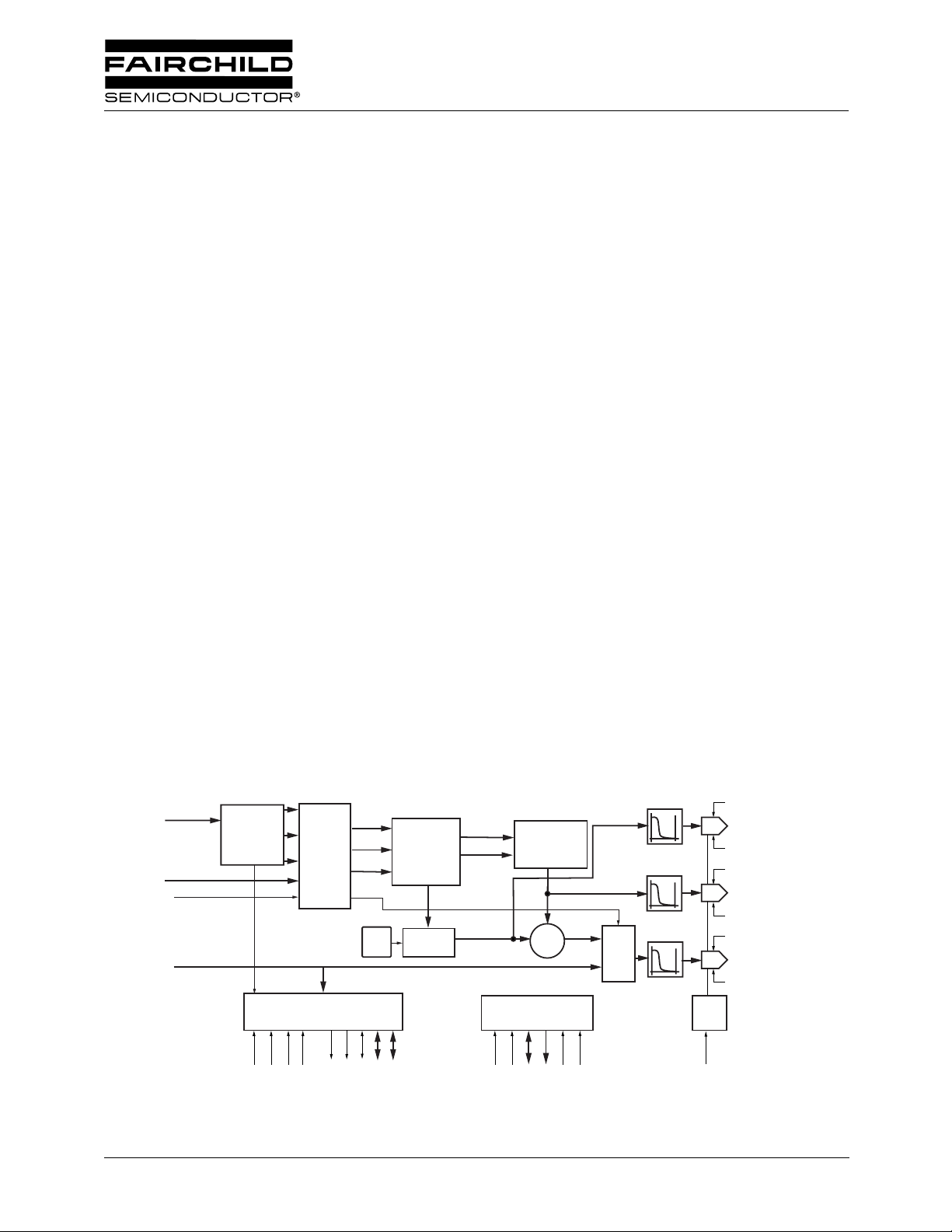
Block Diagram
PD[23:0]
PROCESSER
OL[4:0]
KEY
CVBS[9:0]
PRE-
PXCK
HSIN
OVERLAY
MIXER
FVHGEN
VSIN
DCVEN\
VSOUT
HSOUT
y
cb
cr
Gain
Adjustment
FLD[2:0]
LINE[4:0]
SYNC
INSERT
CC
PDCIN/PDCOUT
C
BYP
LUMA
DAC
REF.
2194001a
LUMA
R
C
CHROMA
R
C
COMPOSITE
R
VREF
REF
BYP
REF
BYP
REF
LUMA
LUMA
CHROMA
COMP
COMP
U
Chroma
V
Modulator
Y
+
MPU
D[7:0]
SERB
RESET
CS/SCL
R/W\/SDA
A[1:0]/SA[1:0]
INTERP.
INTERP.
KEY
MIX
INTERP.
REV. 1.0.0 8/13/03
Page 2

TMC2192 PRODUCT SPECIFICATION
Table of Contents
Features . . . . . . . . . . . . . . . . . . . . . . . . . . . .1
Applications. . . . . . . . . . . . . . . . . . . . . . . . .1
Block Diagram . . . . . . . . . . . . . . . . . . . . . . .1
10 Bit Encoder . . . . . . . . . . . . . . . . . . . . . . .1
List of Figures . . . . . . . . . . . . . . . . . . . . . . .3
List of Tables . . . . . . . . . . . . . . . . . . . . . . . .3
Pin Assignments . . . . . . . . . . . . . . . . . . . . .4
Pin Definitions . . . . . . . . . . . . . . . . . . . . . . .4
Functional Description . . . . . . . . . . . . . . . .7
Input Formats. . . . . . . . . . . . . . . . . . . . . . . . . . . 7
Color Space Matrix . . . . . . . . . . . . . . . . . . . . . . 9
Synchronization Modes . . . . . . . . . . . . . . . . . 10
Propagation Delay . . . . . . . . . . . . . . . . . . . . . . 10
Blanking Control . . . . . . . . . . . . . . . . . . . . . . . 11
Pixel Data Control . . . . . . . . . . . . . . . . . . . . . . 11
Edge Shaping. . . . . . . . . . . . . . . . . . . . . . . . . . 11
Horizontal Programming. . . . . . . . . . . . . . . . . 12
Vertical Timing . . . . . . . . . . . . . . . . . . . . . . . . . 15
Chrominance Processor . . . . . . . . . . . . . . . . . 21
Subcarrier Programming. . . . . . . . . . . . . . . 21
NTSC Subcarrier . . . . . . . . . . . . . . . . . 21
PAL Subcarrier . . . . . . . . . . . . . . . . . . . 21
PAL-M Subcarrier . . . . . . . . . . . . . . . . . 21
Subcarrier Synchronization. . . . . . . . . . . . . 22
SCH Phase Error Correction. . . . . . . . . . . . 22
Burst Envelope . . . . . . . . . . . . . . . . . . . . . . 23
Color-Difference Low-Pass Filters. . . . . . . . 23
Sync and Pedestal Insertion. . . . . . . . . . . . . . 23
Pedestal Enable . . . . . . . . . . . . . . . . . . . . . 23
Pedestal Height. . . . . . . . . . . . . . . . . . . . . . 24
Sync and Blank Insertion . . . . . . . . . . . . . . 24
Interpolation Filters . . . . . . . . . . . . . . . . . . . . . 25
x/Sin(x) Filter . . . . . . . . . . . . . . . . . . . . . . . . . . 25
Output Data Formats. . . . . . . . . . . . . . . . . . . . 25
Digital Composite Output . . . . . . . . . . . . . . . . 26
Ancillary Data. . . . . . . . . . . . . . . . . . . . . . . . . . 26
Operating Modes. . . . . . . . . . . . . . . . . . . . . 27
Layering Engine. . . . . . . . . . . . . . . . . . . . . . . . 28
Overlay Mixer . . . . . . . . . . . . . . . . . . . . . . . 28
Hardware Keying . . . . . . . . . . . . . . . . . . . . . . . 29
Data Keying . . . . . . . . . . . . . . . . . . . . . . . . . . . 29
Parallel Microprocessor Interface . . . . . . . . . 29
Serial Control Port (R-Bus). . . . . . . . . . . . . . . 31
Data Transfer via Serial Interface . . . . . . . . 31
Serial Interface Read/Write Examples . . . . 31
Control Register Map . . . . . . . . . . . . . . . . 33
Control Register Definitions . . . . . . . . . . 35
Absolute Maximum Ratings. . . . . . . . . . .60
Operating Conditions . . . . . . . . . . . . . . . . 60
Electrical Characteristics . . . . . . . . . . . . .62
Switching Characteristics . . . . . . . . . . . .62
System Performance Characteristics . . . 63
Applications Discussion . . . . . . . . . . . . . 63
Layout Considerations . . . . . . . . . . . . . . . . . . 64
Output Low-Pass Filters . . . . . . . . . . . . . . . . . 67
Mechanical Dimensions . . . . . . . . . . . . . . 71
100-Lead MQFP . . . . . . . . . . . . . . . . . . . . . . . . 71
Ordering Information . . . . . . . . . . . . . . . .72
Life Support Policy . . . . . . . . . . . . . . . . . . 72
Closed Caption Insertion . . . . . . . . . . . . . . . . 24
Line Selection . . . . . . . . . . . . . . . . . . . . . . . 24
Parity Generation . . . . . . . . . . . . . . . . . . . . 24
Operating Sequence . . . . . . . . . . . . . . . . . . 24
2 REV. 1.0.0 8/13/03
Page 3

PRODUCT SPECIFICATION TMC2192
List of Figures
Figure 1. Input Formats . . . . . . . . . . . . . . . . . . . . . .7
Figure 2. 24 bit Input Format . . . . . . . . . . . . . . . . . .7
Figure 3. CCIR656 Input Format . . . . . . . . . . . . . . .8
Figure 4. 10 bit Input Format . . . . . . . . . . . . . . . . . .8
Figure 5. 20 bit 4:2:2 Input Format . . . . . . . . . . . . .8
Figure 6. 20 bit 4:4:4 Input Format . . . . . . . . . . . . .8
Figure 7. Propagation Delay through the
Encoder . . . . . . . . . . . . . . . . . . . . . . . . .10
Figure 8. Horizontal Timing . . . . . . . . . . . . . . . . . .13
Figure 9. Horizontal Timing – Vertical Blanking . . .13
Figure 10. Horizontal Timing – 1st Half-line. . . . . . .14
Figure 11. Horizontal Timing – 2nd Half-line . . . . . .14
Figure 12. NTSC Vertical Interval . . . . . . . . . . . . . .15
Figure 13. PAL Vertical Interval . . . . . . . . . . . . . . . .17
Figure 14. PAL-M Vertical Interval . . . . . . . . . . . . . .19
Figure 15. Burst Envelope . . . . . . . . . . . . . . . . . . . .23
Figure 16. Gaussian Filter Response . . . . . . . . . . .23
Figure 17. Interpolation Filter. . . . . . . . . . . . . . . . . .25
Figure 18. Interpolation Filter – Passband
Detail . . . . . . . . . . . . . . . . . . . . . . . . . . .25
Figure 19. X/SIN(X) Filter . . . . . . . . . . . . . . . . . . . .25
Figure 20. Layering Engine . . . . . . . . . . . . . . . . . . .28
Figure 21. Overlay Outputs . . . . . . . . . . . . . . . . . . .29
Figure 22. Data Keying . . . . . . . . . . . . . . . . . . . . . .29
Figure 23. Microprocessor Parallel Port –
Write Timing . . . . . . . . . . . . . . . . . . . . . .30
Figure 24. Microprocessor Parallel Port –
Read Timing . . . . . . . . . . . . . . . . . . . . . .30
Figure 25. Serial Port Read/Write Timing . . . . . . . .31
Figure 26. Serial Interface – Typical Byte
Transfer. . . . . . . . . . . . . . . . . . . . . . . . . .32
Figure 27. Serial Interface – Chip Address . . . . . . .32
Figure 28. Typical Analog Reconstruction Filter . . .63
Figure 29. Overall Response . . . . . . . . . . . . . . . . . .63
Figure 30. Typical Layout . . . . . . . . . . . . . . . . . . . . .65
Figure 31. ST-163E Layout . . . . . . . . . . . . . . . . . . .66
Figure 32. Pass Band . . . . . . . . . . . . . . . . . . . . . . .67
Figure 33. Stop Band. . . . . . . . . . . . . . . . . . . . . . . .67
Figure 34. 2T Pulse . . . . . . . . . . . . . . . . . . . . . . . . .67
Figure 35. Group Delay . . . . . . . . . . . . . . . . . . . . . .67
List of Tables
Table 1. CSM Coefficient Range . . . . . . . . . . . . . 9
Table 2. Expected Output Values for the
CSM with YCBCR Inputs . . . . . . . . . . . . 9
Table 3. PDC Edge Control . . . . . . . . . . . . . . . . 11
Table 4. Horizontal Line Equations. . . . . . . . . . . 12
Table 5. Horizontal Timing Specifications. . . . . . 13
Table 6. Vertical Interval Timing
Specifications . . . . . . . . . . . . . . . . . . . . 14
Table 7. Default Horizontal Timing
Parameters . . . . . . . . . . . . . . . . . . . . . . 15
Table 8. NTSC Field/Line Sequence and
Identification . . . . . . . . . . . . . . . . . . . . . 16
Table 9. PAL Field/Line Sequence and
Identification . . . . . . . . . . . . . . . . . . . . . 18
Table 10. PAL-M Field/Line Sequence and
Identification . . . . . . . . . . . . . . . . . . . . . 20
Table 11. Standard Subcarrier Parameters . . . . . 22
Table 12. Line by Line Pedestal Enable . . . . . . . . 23
Table 13. Closed Caption Line Selection . . . . . . . 24
Table 14. D/A Outputs . . . . . . . . . . . . . . . . . . . . . 25
Table 15. Ancillary Data Format . . . . . . . . . . . . . . 26
Table 16. Ancillary Data Control – Phase . . . . . . 27
Table 17. Ancillary Data Control Frequency. . . . . 27
Table 18. Field Identification and Subcarrier
Reset Modes . . . . . . . . . . . . . . . . . . . . 27
Table 19. Layering and Keying Modes . . . . . . . . . 28
Table 20. Overlay Address Map . . . . . . . . . . . . . . 29
Table 21. Parallel Port Control . . . . . . . . . . . . . . . 30
Table 22. Serial Port Addresses. . . . . . . . . . . . . . 31
Table 23. Control Register Map . . . . . . . . . . . . . . 33
REV. 1.0.0 8/13/03 3
Page 4
TMC2192 PRODUCT SPECIFICATION
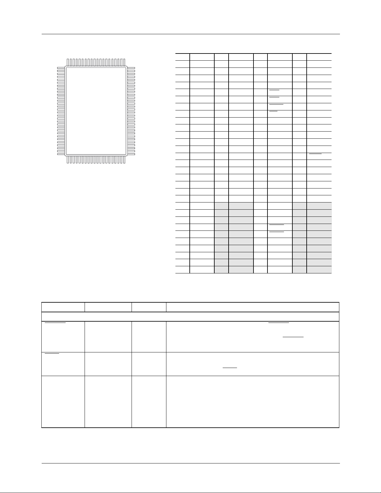
Pin Assignments
100 81
1
30
31 50
80
51
65-6294-14
Pin
1
2
3
4
5
6
7
8
9
10
11
12
13
14
15
16
17
18
19
20
21
22
23
24
25
26
27
28
29
30
Function
V
DDA
COMP
C
BYPCOMP
A
GND
CHROMA
C
BYPCHROM
V
DDA
R
REFCHROM
A
GND
LUMA
C
BYPLUMA
V
DDA
R
REFLUMA
A
GND
A
GND
V
DDA
V
DDA
A
GND
A
GND
KEY
OL4
OL3
OL
2
OL
1
OL0
D
GND
PD23
PD
22
PD
21
PD
20
Pin
31
32
33
34
35
36
37
38
39
40
41
42
43
44
45
46
47
48
49
50
Function
PD
19
PD
18
PD
17
PD16
PD
15
PD
14
PD13
PD12
V
DD
D
GND
PD
11
PD
10
PD9
PD8
PD
7
PD
6
PD5
PD4
PD
3
PD
2
Pin
51
52
53
54
55
56
57
58
59
60
61
62
63
64
65
66
67
68
69
70
71
72
73
74
75
76
77
78
79
80
Function Pin
PD1
PD0
D
GND
V
DD
VSIN
HSIN
DCVEN
SER
CS\/SCL
R/W\/SDA
A1/SA1
A0/SA0
D
7
D6
D
5
D
4
D3
D2
D
1
D0
D
GND
V
DD
PDC
HSOUT
VSOUT
LINE4
LINE3
LINE2
LINE1
LINE0
81
82
83
84
85
86
87
88
89
90
91
92
93
94
95
96
97
98
99
100
Function
FLD2
FLD1
FLD0
CVBS9
CVBS8
CVBS7
CVBS6
CVBS5
CVBS4
CVBS3
CVBS2
CVBS1
CVBS0
RESET
PXCK
V
D
V
R
AGND
DD
GND
REF
REFCOMP
Pin Definitions
Pin Name Pin Number Value Description
CLOCK, SYNC, & CONTROL INPUTS (6 pins)
DCVEN 57 TTL Digital CVBS Output Enable. When DCVEN is LOW, the
Comp2 output prior to the D/A is routed to D7-0, FLD2-1
providing a digital composite output. When DCVEN is HIGH,
D7-0 and FLD2-1 operate in their normal mode.
HSIN 56 TTL Horizontal Sync Input. When operating in slave, Genlock, or
DRS-Lock the TMC2192 will start a new horizontal line with
each falling edge of HSIN.
KEY 20 TTL Hard Key selection. When the control register bit HKEN is set
HIGH and the hardware KEY pin is high, the video data
considered to be the foreground. is routed to the COMP2
output. This control signal is data aligned so that the pixel that is
present on the PD port when KEY signal is latched is at the
midpoint of the key transition. When HKEN is LOW, Key is
ignored.
4 REV. 1.0.0 8/13/03
Page 5
PRODUCT SPECIFICATION TMC2192
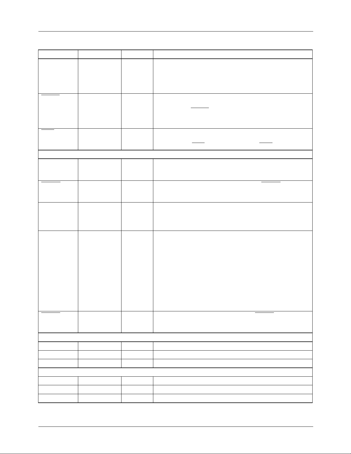
Pin Definitions (continued)
Pin Name Pin Number Value Description
PXCK 95 TTL Pixel Clock Input. PXCK is a clock signal that period is twice
the sample rate of the pixel data. The operating range is 20 to
30 MHz. The clock is internally divided by 2 to generate the
internal pixel clock, PCK. PXCK drives the entire TMC2192
except the asynchronous microprocessor interface.
RESET
VSIN
SYNC & CONTROL OUTPUTS (11 pins)
FLD[2:0] 81–83 TTL Field Identifier. Field Identifier outputs the current field number.
HSOUT 74 TTL Horizontal Sync Output. The alignment of HSOUT to the pixel
LINE[4:0] 76–80 TTL Vertical Blanking Interval Line Identifier. LINE identifies the
PDC 73 TTL Pixel Data Control.
94 TTL Master Chip Reset. When LOW, All outputs are tri-stated and
the internal state machines and control registers are reset. At
rising edge of RESET, all outputs are active, the preset values
will be loaded into the control registers and the internal states
machines start to operate.
55 TTL Vertical Sync Input. When operating in slave, Genlock, or
DRS-Lock the TMC2192 will start a new vertical field with each
falling edge of VSIN that is coincident with HSIN.
For all video standards the field identifier will cycle through the
eight counts.
data port or DCVBS port is controlled by control register
TSOUT.
current line number for the first 31 lines. If the line count is
greater than 31 then LINE is 11111b. The first line with a vertical
serration is considered to be line 0.
When PDCDIR = LOW: At a rising edge, The next pixel starts a
controlled ramp of the PD data. At a falling edge, the pixel prior
is the last PD used in the ramp. The rising edge is determined
by the PDCCNT control register, the falling edge of PDC is
determined by the horizontal timing registers.
When PDCDIR = HIGH: PDCIN is used to override the internal
PDC. When HIGH, the internal PDC controls the blank and
unblank window. When LOW, the video remains blanked
regardless of the internal PDC. All edges have the same ramp
control as the internal PDC.
VSOUT 75 TTL Vertical Sync Output. The alignment of VSOUT to the pixel
data port or DCVBS port is controlled by control register
TSOUT.
DATA INPUTS (39 pins)
CVBS[9:0] 84–93 TTL Composite Data Input
OL[4:0] 21–25 TTL Overlay Control
PD[23:0] 27–38, 41–52 TTL Component Data Input
ANALOG INTERFACE – Video Out (5 pins)
LUMA 10 1.35Vp-p Luma
CHROMA 5 1.35Vp-p Chroma
COMP 2 1.35Vp-p Composite D/A with optional keying
REV. 1.0.0 8/13/03 5
Page 6
TMC2192 PRODUCT SPECIFICATION
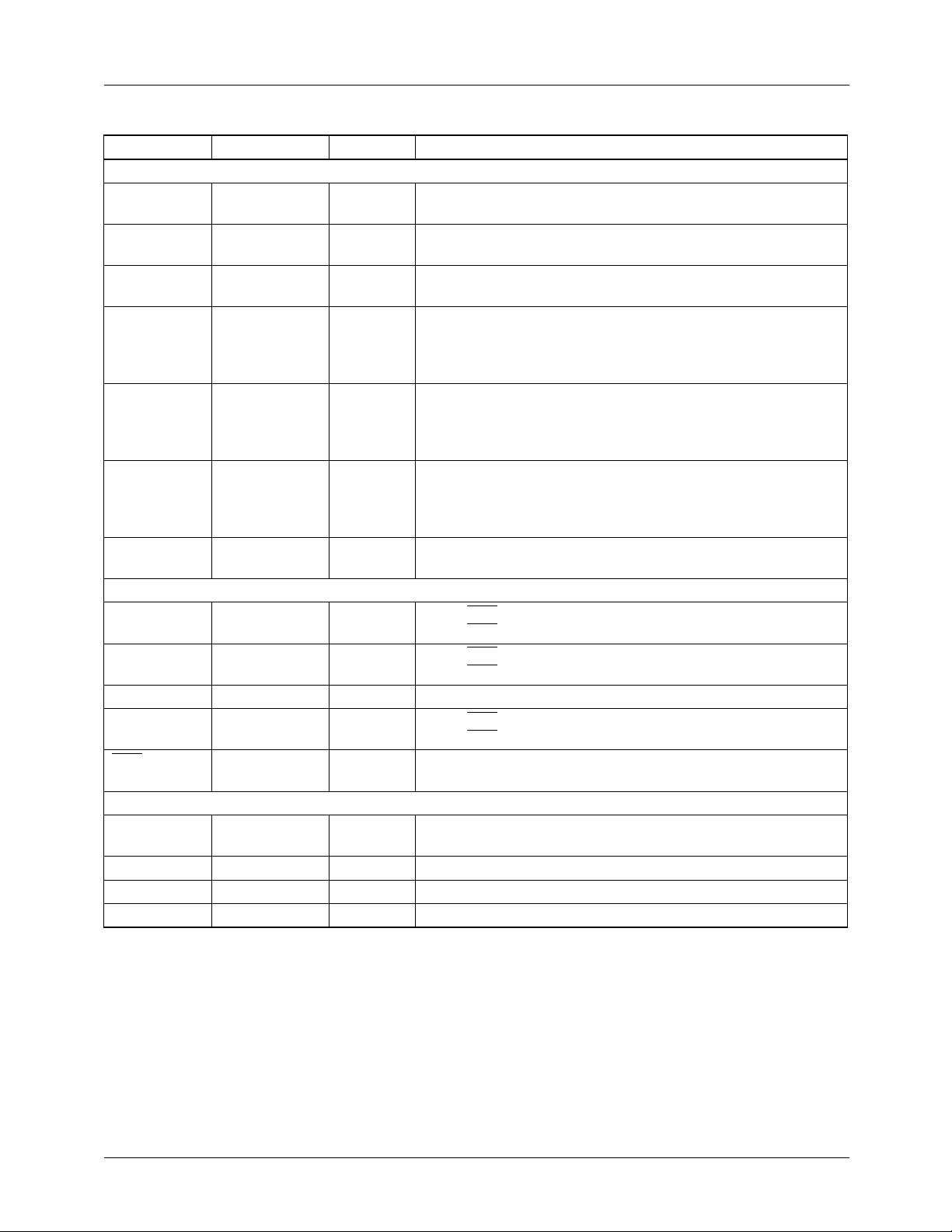
Pin Definitions (continued)
Pin Name Pin Number Value Description
ANALOG INTERFACE – Support (9 pins)
C
BYPLUMA
C
BYPCHROM
C
BYPCOMP
R
REFLUMA
R
REFCHROM
R
REFCOMP
V
REF
MPU INTERFACE (13 pins)
A[1:0]/SA[1:0] 61, 62 TTL When SER (HIGH), OLUT/control/pointer address.
CS/SCL 59 TTL/R-BUS When SER (HIGH), microprocessor port clock.
D[7:0] 63–70 TTL Bi-directional Data Bus.
RW/SDA 60 TTL/R-BUS When SER (HIGH), read/write control.
SER 58 TTL Microprocessor Select. When LOW, the serial interface is
POWER & GROUND (17 pins)
A
GND
D
V
V
GND
DD
DDA
26, 40, 53, 71, 97 0.0V Digital ground
11 0.1 µF Reference Bypass Capacitor for LUMA DAC. Connection
point for 0.1 µF Capacitor.
6 0.1 µF Reference Bypass Capacitor for CHROMA DAC. Connection
point for 0.1 µF Capacitor.
3 0.1 µF Reference Bypass Capacitor for COMPOSITE DAC.
Connection point for 0.1 µF Capacitor.
13 1210 Ohm Current Setting Resistor. Connection point for external current
setting resistor for LUMA DAC. The resistor is connected
between R
inversely proportional to the value of R
8 1210 Ohm Current Setting Resistor. Connection point for external current
setting resistor for CHROMA DAC. The resistor is connected
between R
inversely proportional to the value of R
99 1210 Ohm Current Setting Resistor. Connection point for external current
setting resistor for COMPOSITE DAC. The resistor is connected
between R
inversely proportional to the value of R
98 1.235 V Voltage Reference Input. External voltage reference input,
internal voltage reference output, nominally 1.235V.
When SER (LOW), SA[1:0] of serial chip address SA[6:0].
When SER (LOW), serial bus clock.
When SER (LOW), serial bus bi-directional data.
enabled. When HIGH, the parallel interface is enabled.
4, 9, 14, 15, 18,
19, 100
39, 54, 72, 96 +5.0V Digital positive power supply
1, 7, 12, 16, 17 +5.0V Analog positive power supply
0.0V Analog ground
REFLUMA
REFCHROM
REFCOMP
and GND. Output video levels are
and GND. Output video levels are
and GND. Output video levels are
.
REF2
REFCHROM
REFCOMP
.
.
6 REV. 1.0.0 8/13/03
Page 7
PRODUCT SPECIFICATION TMC2192
Functional Description
Input Formats
Control Registers for this section
Address Bit(s) Name
0x05 7 D1OFF
0x05 6-4 INMODE
0x06 0 TSOUT
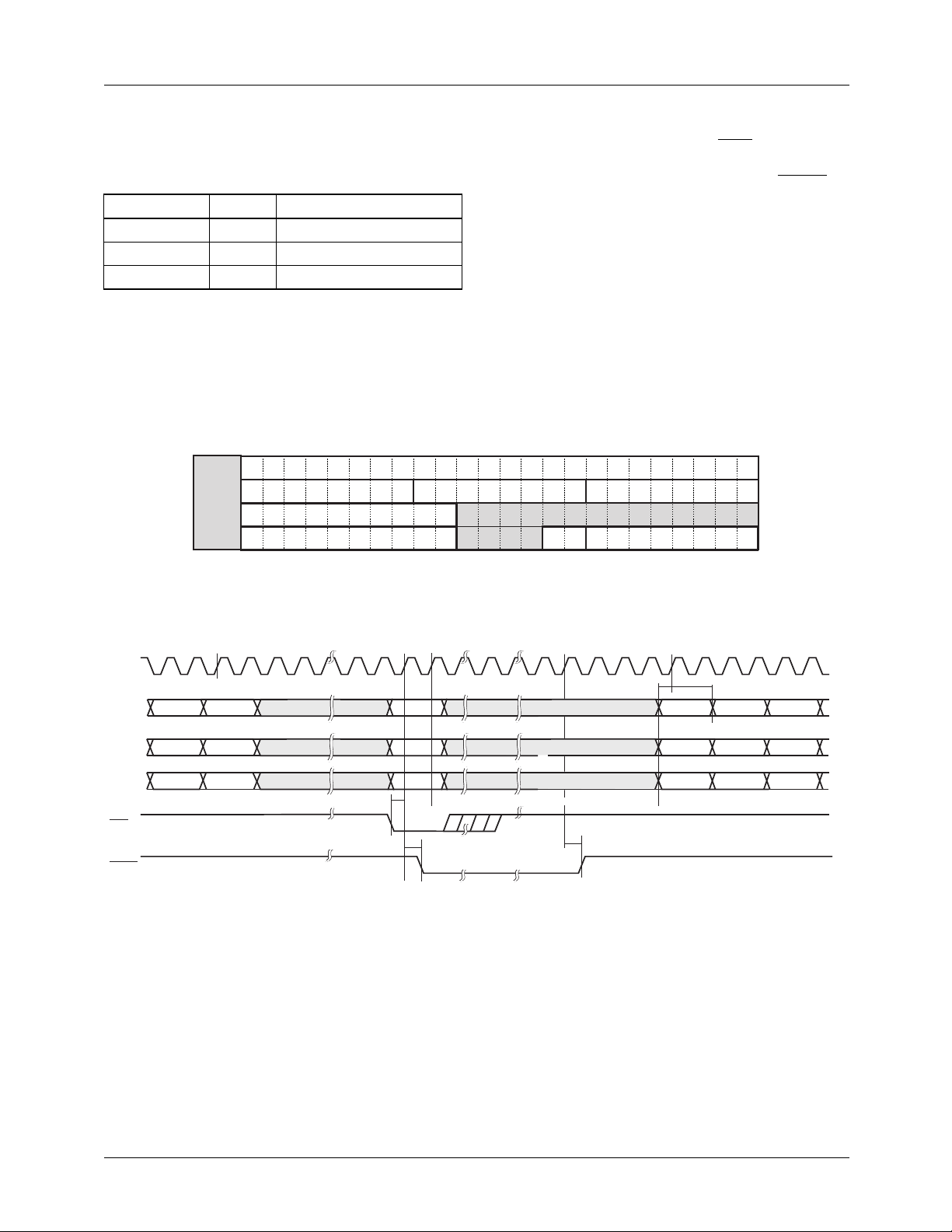
The TMC2192 supports YCBCR component sources on the
pixel data port. YCBCR input sources are supported in 10 bit
4:2:2, 20 bit 4:2:2, 20 bit 4:4:4, and 24 bit 4:4:4. In the 4:2:2
cases the color difference components are linearly interpolated to 4:4:4 internally.
INMODE
23
777
00
01
9
1x
9
C
B
YC C
BR
YC C
BR
15 897
16
0
Figure 1. Input Formats
Demuxing of multiplexed data streams depends on which
synchronization mode the encoder is operating in. For slave
and genlock modes the falling edge of HSIN must be LOW
prior to the CB data in order to demux the data correctly. For
master mode synchronization the falling edge of HSOUT
must be LOW prior to the Y data in order to demux the data
correctly. Finally, in 656 mode the demuxing of the data
stream is determined by the TRS codes, the first sample after
the TRS is considered a C
sample of the CB Y CR YI
B
packet.
The control register D1OFF controls the formatting of the
incoming luminance data at the pixel data port. When
D1OFF is HIGH a blanking level of 64
is subtracted from
10
the luminance and when D1OFF is LOW the incoming the
pixel data is passed through. The inversion of the MSB’s on
the CB and CR components is controlled by the INMODE
control register.
PD 0
C
R
1
0Y90
Y
000
2
2192002A
1. INMODE = 00, PD[7:0] = PD[23:16] = CB, PD[15:8] = C
PXCK
PD[7:0]
PD[23:16]
PD[15:8]
HSIN
HSOUT
(TSOUT = 1)
Y
n-1
C
B
C
n-1
R
Y
n
C
n-1
n
B
C
n
R
Y
0
C
0
B
C
0
R
t
SP
t
DO
Figure 2. 24 Bit Input Format
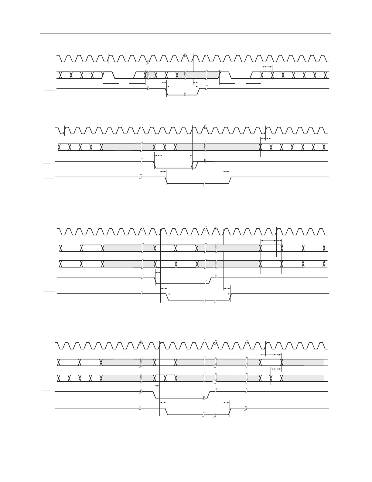
2. INMODE = 01, PD[23:14] = YCBCR running at 27MHz.
The PD port is clocked at twice the pixel rate, with the data
organized as CB Y CR Y, with the cosited Y's following the
CB's. In its CCIR-656 time base mode, the demuxed CB, Y,
and CR data is synchronized to the SAV preamble. The first
R
t
DO
x = (SY+BR+BU+CBP)*2
t
S
Y
C
B
C
R
t
H
Y
x
x
x
x+1
C
x+1
B
C
x+1
R
Y
x+2
C
x+2
B
C
x+2
R
1280n = (SY+BR+BU+CBP+AV)*2
data value, after the SAV preamble, is treated as a CB data
point in the multiplexed CB, Y, CR Y , D1 data stream.
Note: Figure 3, pixel numbering, reflects the SMPTE-125M
pixel numbering.
2192003A
REV. 1.0.0 8/13/03 7
Page 8
TMC2192 PRODUCT SPECIFICATION
PXCK
PD[23:14]
Y
C
718
B718
Y
C
719
R718
00
FF
FV
00
EAV
HSOUT
(TSOUT = 1)
n = (SY+BR+BU+CBP+AV)*2
PXCK
PD[23:14]
Y
C
Bn
Y
C
n
n+1
Rn
HSIN
HSOUT
(TSOUT = 1)
3. INMODE = 11, PD[9:0] = Y, PD[23:14] = CB/CR
n = (SY+BR+BU+CBP+AV)*2
PXCK
PD[9:0]
Y
Y
n
n+1
0
C
Y
B736
1
736
t
DO
128
t
t
HS
DO
Figure 3. CCIR656 Input Format
0
C
Y
B0
0
t
SP
t
DO
t
HP
Figure 4. 10 bit Input Format
0
Y
0
Y
1
(SY+BR+BU+CBP)*2
t
t
S
H
C
C
FF
00
00
FV
0
Y
B0
0
Y
R0
1
Y
C
2
B2
SAV
65-6294-04
128
t
DO
128
x = (SY+BR+BU+CBP)*2
t
S
C
Bx
x = (SY+BR+BU+CBP)*2
t
S
Y
t
H
Y
C
Y
x
Rx
x+1
t
H
Y
x
x+1
C
Bx+2
65-6294-05
Y
x+2
Y
x+2
PD[23:14]
C
C
Bn
Rn
C
t
SP
C
B0
R0
HSIN
t
HSOUT
(TSOUT = 1)
DO
t
HS
Figure 5. 20 bit 4:2:2 Input Format
4. INMODE = 10, PD[9:0] = Y at PCK, PD[23:14] = CB-CR at PXCK
n = (SY+BR+BU+CBP+AV)*2
PXCK
PD[9:0]
PD[23:14]
C
B
n
HSIN
HSOUT
(TSOUT = 1)
Y
Y
n
n+1
C
C
C
n
n+1
R
B
Rn+1
0
Y
0
C
C
B
0
0
R
t
SP
t
DO
Figure 6. 20 bit 4:4:4 Input Format
C
t
DO
128
x = (SY+BR+BU+CBP)*2
t
S
Y
t
S
C
B
x
t
DO
C
Bx
x
Rx
t
H
t
H
C
x
R
C
Bx+2
65-6294-06
65-6294-07
8 REV. 1.0.0 8/13/03
Page 9
PRODUCT SPECIFICATION TMC2192
Color Space Matrix
Control Registers for this section
Address Bit(s) Name
0x30 7-0 MCF1L
0x33 7-0 MCF2L
0x35 7-0 MCF3L
0x3A 7-4 MCF1M
0x3B 2-0 MCF2M
0x3C 2-0 MCF3M
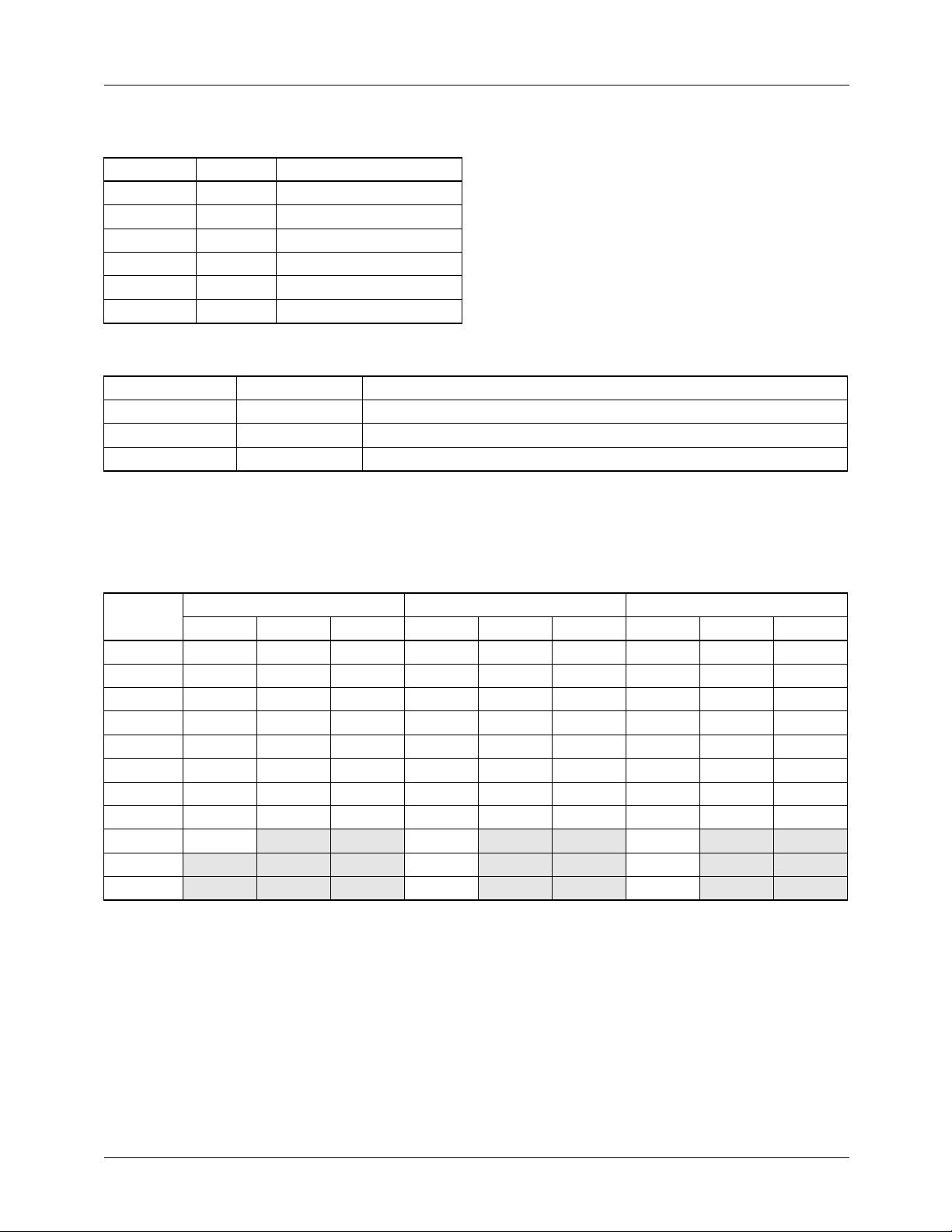
Table 1. CSM Coefficient Range
Coefficient Gain Range Comment
MCF1 0 to 2
MCF2 0 to 1 11 bit coefficient.
MCF3 0 to 1 11 bit coefficient.
Matrix configuration:
Y
composite
U = MCF2 * C
V = MCF3 * C
The color space matrix consists of 3 multipliers with independently adjustable coefficients, and a resolution of
0.00049 (1/2048). The amount of gain varies among coefficients, Table 1 summarizes the gain for each coefficient.
= MCF1 * Y
in
B
R
To aid in the programming of the color space matrix Table 2
provides a set of default input and output values for 100%
color bars. The component values given will be after the pre-
Table 2. Expected Output Values for the CSM with YCBCR Inputs
Inputs 5:2 Outputs 7:3 Outputs
Color
White 876 0 0 536 0 0 568 0 0
Yellow 776 -448 73 475 -235 54 503 -249 57
Cyan 614 151 448 376 79 -332 407 84 -351
Green 514 -297 -375 315 -156 -278 340 -165 -294
Magenta 362 297 375 222 156 278 240 165 294
Red 262 -151 448 160 -79 332 173 -84 351
Blue 100 448 -73 61 235 -54 66 249 -57
Black 000000000
Blank 64 240 256
Pedestal 44 0
Sync 8 12
YC
B
C
R
YUVYUV
processing block and prior to the sync and pedestal insertion.
The blank, pedestal, and sync values are given as a reference.
Table 4 gives the default coefficients values for the CSM.
REV. 1.0.0 8/13/03 9
Page 10
TMC2192 PRODUCT SPECIFICATION
Synchronization Modes
Control Registers for this section
Address Bit(s) Name
0x06 5-3 MODE
0x06 1 TOUT
0x06 0 TSOUT
The TMC2192 offers a variety of synchronization modes;
these are master, slave, genlock, 656 mode, and DRS-Lock.
In master mode, the TMC2192 generates its own timing and
the synchronization is supplied externally by HSOUT and
VSOUT
derives its timing from the input pins HSIN, VSIN. In 656
mode the timing is driven by the synchronization codes
embedded into the data stream.
Master
The TMC2192 drives the output pins HSOUT and VSOUT
to synchronize the incoming video. A new color frame starts
at the rising edge of RESET. The encoder always starts at the
1st vertical serration in field 8 and will freerun the field and
line sequence. The control register bit SRESET can be used
to synchronize the start of the field and line sequence in master mode by resetting the FVHGEN state machine. Output
synchronization signal VSOUT can operate in a traditional
sync mode or in a MPEG style field toggle mode.
Slave
The TMC2192 is driven by the input synchronization pins
HSIN and VSIN. When the falling edge of HSIN and VSIN
occurs at the same rising edge of PXCK the TMC2192 will
start a new field.VSIN can be either a traditional pulse or the
MPEG style field toggle. In both cases the TMC2192 will
flywheel through fields 2, 4, 6, and 8 synchronizing only to
fields 1, 3, 5, and 7.
signals. In slave and genlock modes the TMC2192
CCIR656
The TMC2192 derives all synchronization from the embedded TRS (timing reference signals) information. Blanking of
selected lines is determined by the v bit of the TRS. However
the control registers VBIENx can override and blank the
active video portion of VBI lines regardless of the state of the
v-bit.
Genlock
The TMC2192 is driven by the input synchronization pins
HSIN
and VSIN. When the falling edge of HSIN and VSIN
occurs at the same rising edge of PXCK the TMC2192 will
start a new field.VSIN
can be either a traditional pulse or the
MPEG style field toggle. In both cases the TMC2192 will
flywheel through fields 2, 4, 6, and 8 synchronizing only to
fields 1, 3, 5, and 7. The TMC2192 collects GRS data and
resets its subcarrier phase and frequency to the data embedded in the GRS stream. The GRS detection occurs only on
the CBVS port.
DRS
The TMC2192 is driven by the input synchronization pins
HSIN and VSIN. When the falling edge of HSIN and VSIN
occurs at the same rising edge of PXCK the TMC2192 will
start a new field.VSIN can be either a traditional pulse or the
MPEG style field toggle. In both cases the TMC2192 will
flywheel through fields 2, 4, 6, and 8 synchronizing only to
fields 1, 3, 5, and 7. Subcarrier phase adjustment is determined by the DRS data. The DRS detection can occur on
either the CBVS port or the pixel data port.
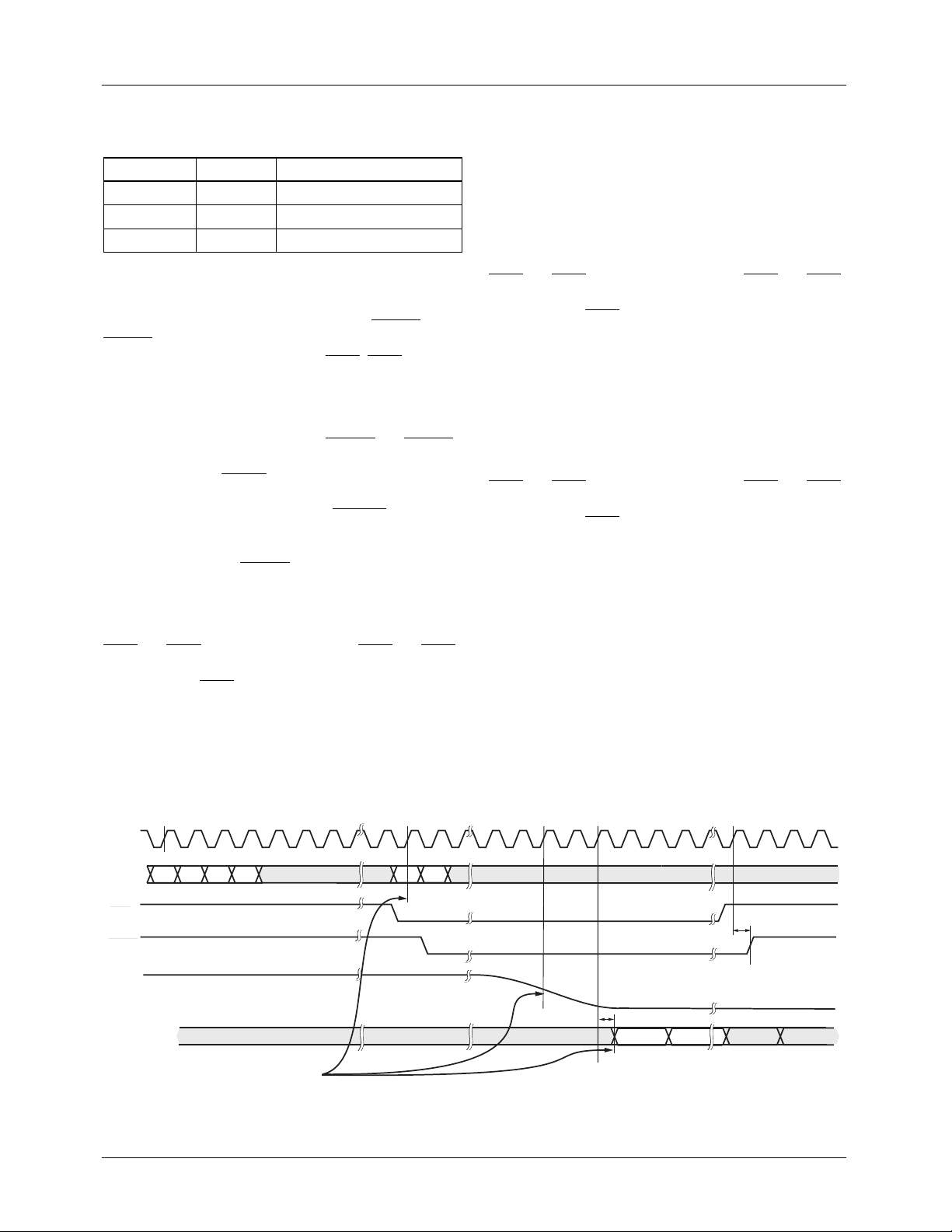
Propagation Delay
The propagation delay from the pixel data (PD) input to the
D/A output is 64 PXCK’s. Figure 8 shows the propagation
delay for both master and slave synchronization modes. For
CCIR656 data streams, pixel 736 (pixel 0 in Figure 8) is the
midpoint of sync and is 32 PXCK’s (24 PXCK’s in PAL)
after the EAV TRS.
n = (SY+BR+BU+CBP+AV)*2
PXCK
C
PD[23:14]
HSIN
HSOUT
(TSOUT = 1)
DACx
(ANALOG)
DCVBS
(D[7:0],FLD[2:1])
Bn
Y
C
n
Y
n+1
Rn
Midpoint of the
Falling Edge of Sync
0
C
Y
B0
0
63 65
t
DO
COMP
0
COMP
128
t
DO
1
65-6294-09
Figure 7. Propagation Delay through the Encoder
10 REV. 1.0.0 8/13/03
Page 11
PRODUCT SPECIFICATION TMC2192
Blanking Control
Control Registers for this section
Address Bit(s) Name
0x04 1-0 PDRM
0x06 2 PDCDIR
0x18 4-0 VBIENF1
0x19 4-0 VBIENF2
0x1F 7-0 PDCCNT
The content of VBIENFx[4:0] selects the first line to contain
an active video region in each field, all subsequent lines for
the remainder of the field are active. To blank an entire field,
the user zeroes the VBIENFx[4:0] control register. In
CCIR656 slave mode, the user can selectively blank any
enabled line by setting its TRS V bit HIGH. For 525-line
systems, NTSC line numbering is employed, with the first
vertical serration starting on line 4. PAL line numbering is
used with 625-line systems, with each field's line 1 being the
start of the first vertical serration.
Any line(s) enabled by the closed caption control are automatically unblanked for the closed caption waveform, irrespective of the corresponding values of VBIENF.
Pixel Data Control
The pixel data control has two modes of operation, as an
input or as an output. The mode of operation is determined
by the PDCDIR control register. When PDC is an input the
internally generated PDC is ANDed with the PDC pin. This
allows the user to blank any active video regions. When PDC
is an output, the internally generated PDC is the output for
the PDC pin.
The internal PDC control will toggle to a logic HIGH at the
pixel specified by PDCNT and toggle to a logic LOW four
pixels prior to the end of the active video region. The starting
point and ending point of the active video region (VA) are
determined by the control registers 10h to 1Fh. When PDC is
used as an input, the sloped edge of the active video region
will occur on the next four pixels following the toggle point.
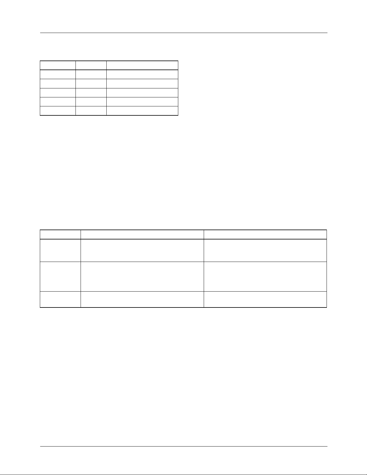
Edge Shaping
The TMC2192 has three modes of sloped edges on the active
video region and are controlled by PDRM control register.
Table 3. PDC Edge Control
PDRM[1:0] Slope type at PDC (HIGH) Slope type at PDC (LOW)
00 The following four pixels have the weighting of
1/8, 1/2, 7/8 and 1 for NTSC and 1/8, 3/8, 5/8,
and 7/8 for PAL.
01 The fifth pixel is sampled and scaled 1/8, 1/2,
7/8 and 1 over the next four pixels for NTSC
and 1/8, 3/8, 5/8, and 7/8 over the next four
pixels for PAL.
1x Slope is off, edge control is dictated by the PD
stream from active video start
The following four pixels have the weighting of
1, 7/8, 1/2, and 1/8 for NTSC and 7/8, 5/8, 3/8,
and 1/8 for PAL.
The fifth pixel s sampled and scaled 1, 7/8, 1/2
and 1/8 over the next four pixels for NTSC and
7/8, 5/8, 3/8, and 1/8 over the next four pixels
for PAL.
Slope is off, edge control is dictated by the PD
stream to active video end
REV. 1.0.0 8/13/03 11
Page 12
TMC2192 PRODUCT SPECIFICATION
Horizontal Programming
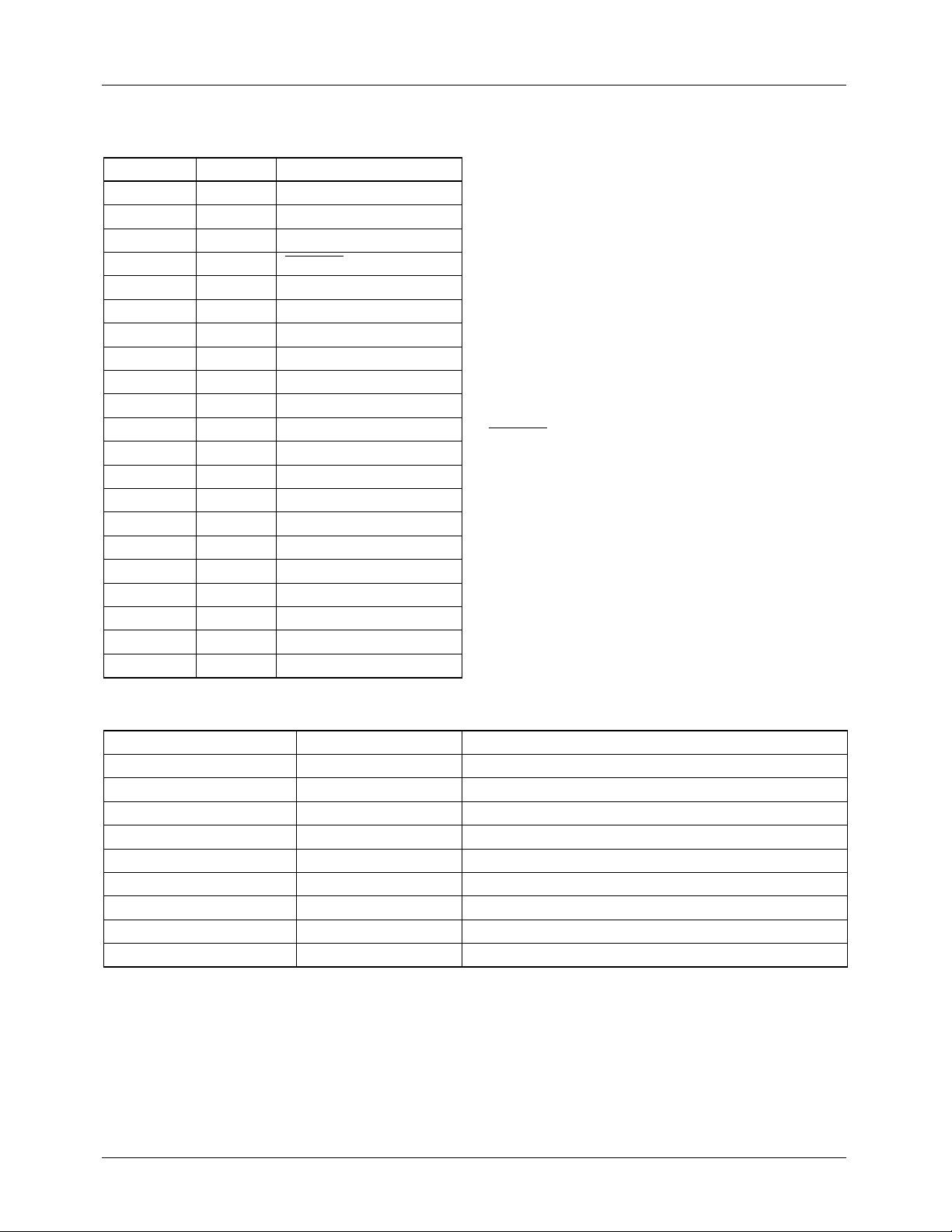
Control registers for this section
Address Bit(s) Name
0x06 7-6 FORMAT
0x19 7 SHORT
0x19 6 T512
0x19 5 HALFEN
0x20 7-0 SY
0x21 7-0 BR
0x22 7-0 BU
0x23 7-0 CBP
0x24 7-0 XBP
0x25 7-0 VA
0x26 7-0 VC
0x27 7-0 VB
0x28 7-0 EL
0x29 7-0 EH
0x2A 7-0 SL
0x2B 7-0 SH
0x2C 7-0 FP
0x2D 7-6 XBP (MSB’s)
0x2D 5-4 VA (MSB’s)
0x2D 3-2 VB (MSB’s)
0x2D 1-0 VC (MSB’s)
Horizontal interval timing is fully programmable and is
established by loading the timing registers with the duration
of each horizontal element. The duration is expressed in
PCK clock cycles. In this way, any pixel clock rate between
10 MHz and 15 MHz can be accommodated, and any desired
standard or non-standard horizontal video timing may be
produced.
Horizontal timing parameters can be calculated as follows:
t = N x ( PCK period )
= N x ( 2 x PXCK period )
where N is the value loaded into the appropriate timing
register, and PCK is the pixel clock period.
When programming horizontal timing, subtract 5 PCK
periods from the calculated values of CBP and add 5 PCK
periods to the calculated value for VA. The control register
HALFEN
NTSC, PAL-M and line 23 for all other PAL standards when
it is LOW.
enables the 1st half line (UBV) on line 283 for
Table 4. Horizontal Line Equations
Line Type Line ID Line Length Equals
EE 00 EL + EH + EL + EH
SE 02 SL + SH + EL + EH
SS 03 SL + SH + SL + SH
ES 01 EL + EH + SL + SH
EB 10 EL + EH + EL + EH
UBB, -BB 0D, 05 SY + BR + BU + CBP + VA + FP
UVV, -VV 0F, 07 SY + BR + BU + CBP + VA + FP
UVE, -VE 0C, 04 SY + BR + BU + CBP + VC + FP + EL + EH
UBV 0E SY + BR + BU + XBP + VB + FP
12 REV. 1.0.0 8/13/03
Page 13
PRODUCT SPECIFICATION TMC2192
SY
BR BU CBP VA FP
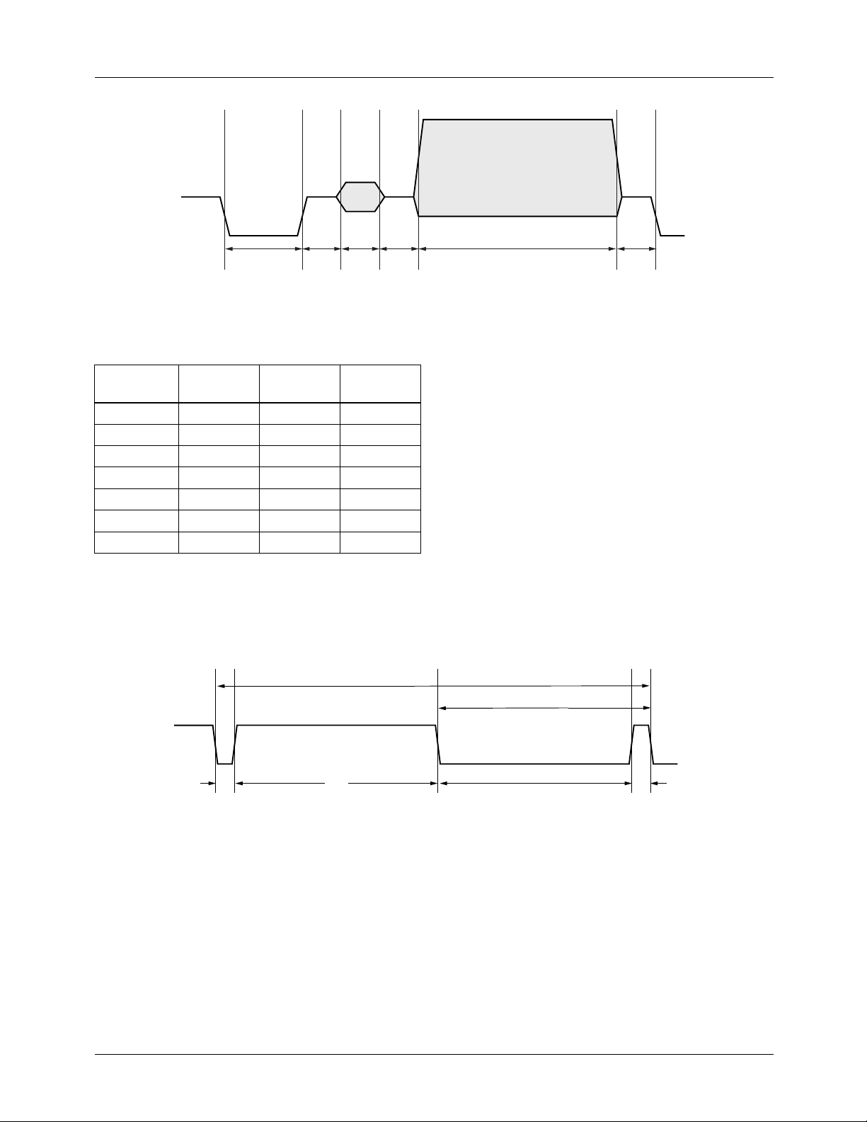
Figure 8. Horizontal Timing
Table 5. Horizontal Timing Specifications
Parameter
NTSC-M
(µs)
PAL-I
(µs)
PAL-M
(µs)
FP 1.5 1.65 1.9
SY 4.7 4.7 4.95
BR 0.6 0.9 0.9
BU 2.5 2.25 2.25
CBP 1.6 2.55 1.8
VA 52.6556 51.95 51.692
H 63.5556 64.0 63.492
Vertical interval timing is also fully programmable, and is
established by loading the timing registers with the duration’s of each vertical timing element, the duration expressed
in PCK clock cycles. In this way as with horizontal program-
65-6294-10
ming, any pixel rate between 10 and 15 Mpps can be accommodated, and any desired standard or non-standard vertical
video timing may be produced.
Like horizontal timing parameters, vertical timing parameters are calculated as follows:
t = N x ( PCK period )
= N x ( 2 x PXCK period )
where N is the value loaded into the appropriate timing register, and PCK is the pixel clock period.
The vertical interval comprises several different line types
based upon H, the Horizontal line time.
H = (2 x SL) + (2 x SH) [Vertical sync pulses]
= (2 x EL) + (2 x EH) [Equalization pulses]
H
H/2
EL
EH SL SH
65-6294-11
Figure 9. Horizontal Timing – Vertical Blanking
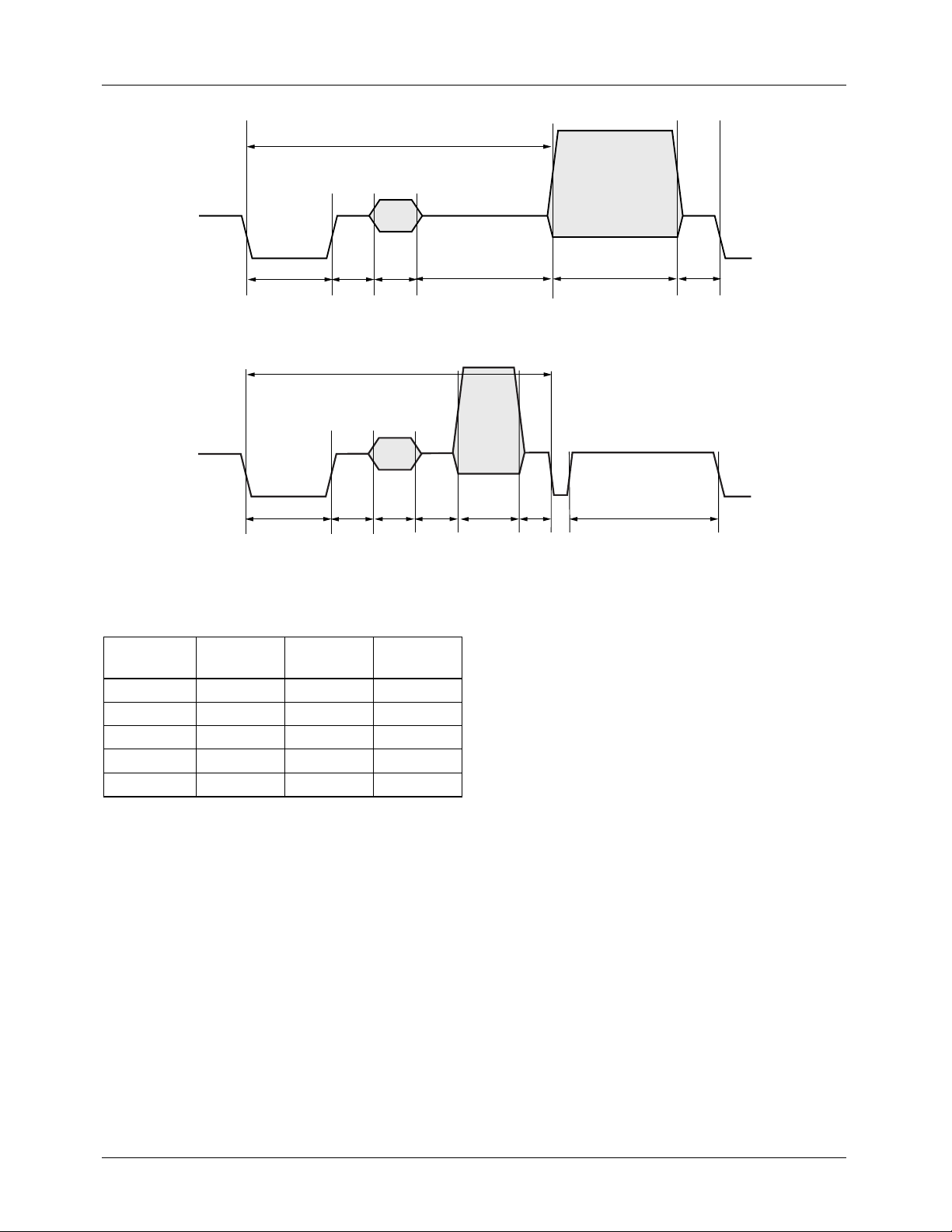
The VB and VC control registers are added to produce the
half-lines needed in the vertical interval at the beginning and
end of some fields. These must properly mate with components of the normal lines.
REV. 1.0.0 8/13/03 13
Page 14
TMC2192 PRODUCT SPECIFICATION
H/2
SY
SY
BR BU XBP
Figure 10. Horizontal Timing – 1st Half-line
BR
Figure 11. Horizontal Timing – 2nd Half-line
Table 6. Vertical Interval Timing Specifications
NTSC-M
Parameter
(µs)
H 63.5556 64 63.492
EH 29.4778 29.65 29.45
EL 2.3 2.35 2.3
SH 4.7 4.7 4.65
SL 27.1 27.3 27.1
PAL-I
(µs)
H/2
BU
CBP VC FP
PAL-M
(µs)
EL
VB FP
65-6924-12
EH
65-6294-13
14 REV. 1.0.0 8/13/03
Page 15
PRODUCT SPECIFICATION TMC2192
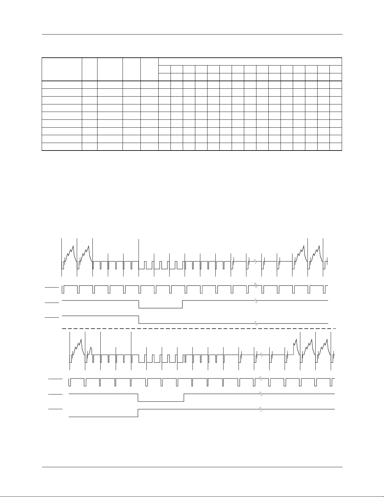
Table 7. Default Horizontal Timing Parameters
Field
Horizontal
Standard
NTSC sqr. pixel 59.94 15.734266 12.27 24.54 3A 07 1F 0F 23 8B 05 77 1C 6A 4C 3A 12 65 52
NTSC CCIR-601 59.94 15.734266 13.50 27.00 40 08 22 11 44 CB 1E 98 1F 8E 6D 40 14 65 59
NTSC 4x F
PAL sqr. pixel 50.00 15.625000 14.75 29.50 45 0D 21 21 6D 03 2B B7 23 B5 93 45 19 75 61
PAL CCIR-601 50.00 15.625000 13.50 27.00 40 0C 1E 22 4D BE 0E 93 20 90 70 40 16 65 59
PAL 15 Mpps 50.00 15.625000 15.00 30.00 46 0D 22 21 73 11 31 BF 23 BD 9A 47 19 75 62
PAL-M sqr.pixel 60.00 15.750000 12.50 25.01 3E 0B 1C 13 26 86 FE 8B 1D 70 53 3A 18 61 52
PAL-M CCIR-601 60.00 15,750000 13.50 27.00 44 0C 1E 13 26 Bf 12 99 1F 8E 6E 3F 1A 65 57
PAL-M 4x F
SC
Rate
(Hz)
59.94 15.734266 14.32 28.64 43 09 24 12 54 F7 30 B5 21 A6 84 43 15 65 5F
60.00 15,750000 14.30 28.60 47 0D 20 15 4C E8 22 AC 21 A5 84 42 1B 65 5D
SC
Freq.
(KHz)
Pixel
Rate
(Mpps)
PXCK
SY BR BU CBP XBP VA VC VB EL EH
Freq.
20 21 22 23 24 25 26 27 28 29 2A 2B 2C 2D 2F
(MHz)
Timing Register (hex)
2SL2
SH FP Note CBL
Notes:
1. XBP, VA, VC, and VB are 10 bit values. The 2 MSBs for these four variables are in Timing Register 2D.
2. EH and SL are 9 bit values. A most significant "1" is forced by the TMC2192 since EH and SL must range from 256 to 511.
EH and SL may be extended to 767. Only the eight LSBs are stored in Timing Registers 29 and 2A.
3. Every calculated timing parameter has a minimum value of 5 except EH and SL which have minimum values of 256.
Vertical Timing
The vertical timing is controlled by the FORMAT control
register, which dictates the field and line sequence.
524
525
FIELDS 1 AND 3
22
HSOUT
VSOUT
(TOUT = 1)
VSOUT
(TOUT = 0)
HSOUT
VSOUT
(TOUT = 1)
VSOUT
(TOUT = 0)
UVV
UVVEEEEEEEEESEESSSSSSSSSESSEEEEEEEEEBEE
262
UVV
263
26412652266326742685269627072718272
UVE
FIELDS 2 AND 4
Figure 12. NTSC Vertical Interval
•••
9
UBB
27310•••
UBB
19
UBB
UBB
282
UBB
UVV
UVV
2832028421285
UVV
UBV
UVV
65-6294-15
REV. 1.0.0 8/13/03 15
Page 16
TMC2192 PRODUCT SPECIFICATION
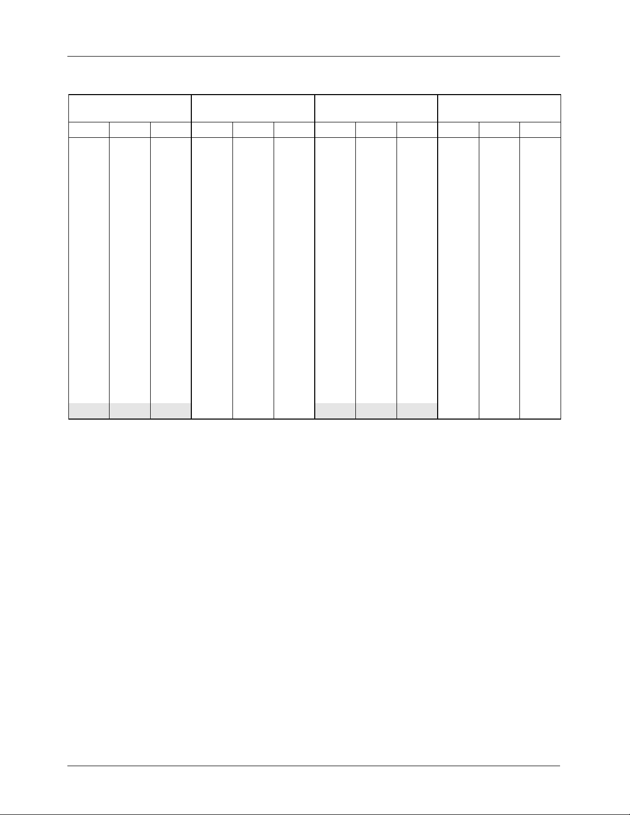
Table 8. NTSC Field/Line Sequence and Identification
Field 1
FIELD ID = x00
Line ID LTYPE Line ID LTYPE Line ID LTYPE Line ID LTYPE
4 SS 03 266 ES 01 4 SS 03 266 ES 01
5 SS 03 267 SS 03 5 SS 03 267 SS 03
6 SS 03 268 SS 03 6 SS 03 268 SS 03
7 EE 00 269 SE 02 7 EE 00 269 SE 02
8 EE 00 270 EE 00 8 EE 00 270 EE 00
9 EE 00 271 EE 00 9 EE 00 271 EE 00
10 UBB 0D 272 EB 10 10 UBB 0D 272 EB 10
… UBB 0D 273 UBB 0D … UBB 0D 273 UBB 0D
19 UBB 0D … UBB 0D 19 UBB 0D … UBB 0D
20 UBB 0D 282 UBB 0D 20 UBB 0D 282 UBB 0D
21 UVV 0F 283 UBV 0E 21 UVV 0F 283 UBV 0E
22 UVV 0F 284 UVV 0F 22 UVV 0F 284 UVV 0F
… UVV 0F … UVV 0F … UVV 0F … UVV 0F
262 UVV 0F 524 UVV 0F 262 UVV 0F 524 UVV 0F.
263 UVE 0C 525 UVV 0F 263 UVE 0C 525 UVV 0F
264 EE 00 1 EE 00 264 EE 00 1 EE 00
265 EE 00 2 EE 00 265 EE 00 2 EE 00
Field 2
FIELD ID = x01
3EE00 3EE00
FIELD ID = x10
Field 3
Field 4
FIELD ID = x11
EE Equalization pulse
SE Half-line vertical sync pulse, half-line equalization pulse
SS Vertical sync pulse
ES Half-line equalization pulse, half-line vertical sync pulse
EB Equalization broad pulse
UBB Black burst
UVV Active video
UVE Half-line video, half-line equalization pulse
UBV half-line black, half-line video
16 REV. 1.0.0 8/13/03
Page 17
PRODUCT SPECIFICATION TMC2192
HSOUT
VSOUT
(TOUT = 1)
VSOUT
(TOUT = 0)
HSOUT
VSOUT
(TOUT = 1)
VSOUT
(TOUT = 0)
623
622
UVV
309 310
UVV
623
622
FIELDS 1 AND 5
624 625 1
-VE EE EE SS SS SE EE EE -BB
FIELDS 2 AND 6
311 312 313
-VV EE EE ES SS SS EE EE EB
FIELDS 3 AND 7
23
314 315
45 67
UBB
316 317 318 319
UBB
•••
•••
320
23
24
22
UBVUBB UVV UVV
UVV
•••
334 335
•••
UBBUBB UVV UVV
UBB
23
24
25 26
336 337
25 26
HSOUT
VSOUT
(TOUT = 1)
VSOUT
(TOUT = 0)
HSOUT
VSOUT
(TOUT = 1)
VSOUT
(TOUT = 0)
624 625 1
-VV -VE EE EE SS SS SE EE EE UBB UBB
309 310
UVV
UVV EE EE ES SS SS EE EE EB
FIELDS 4 AND 8
311 312 313 314 315 316 317
23
45 67
318
319
-BB
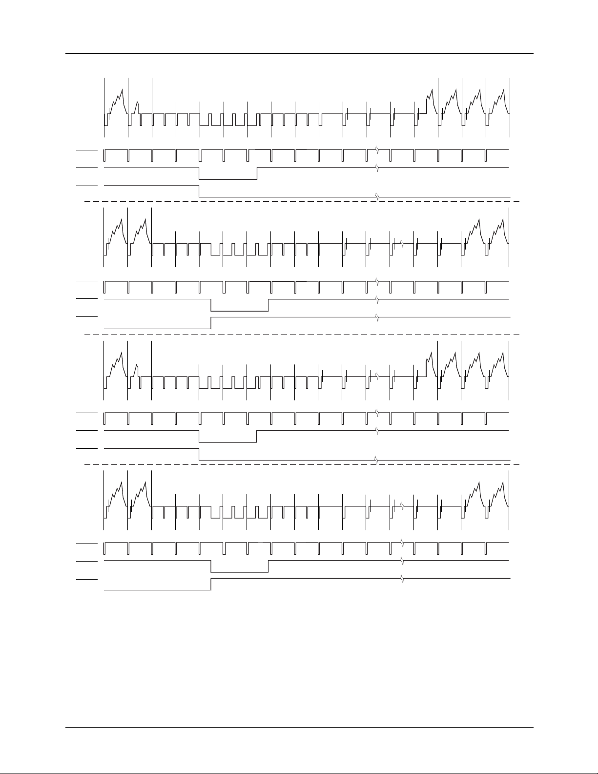
Figure 13. PAL Vertical Interval
•••
22
•••
320 334 335
UBVUBB UVV UVV
UVV
•••
•••
UBBUBB UVV UVV
UBB
336 337
65-6294-16
REV. 1.0.0 8/13/03 17
Page 18

TMC2192 PRODUCT SPECIFICATION
Table 9. PAL Field/Line Sequence and Identification
Field 1 & 5
FIELD ID = 000, 100
Field 2 & 6
FIELD ID = 001, 111
Field 3 & 7
FIELD ID = 010, 110
Field 4 & 8
FIELD ID = 011, 111
Line ID LTYPE Line ID LTYPE Line ID LTYPE Line ID LTYPE
1 SS 03 313 ES 01 1 SS 03 313 ES 01
2 SS 03 314 SS 03 2 SS 03 314 SS 03
3 SE 02 315 SS 03 3 SE 02 315 SS 03
4 EE 00 316 EE 00 4 EE 00 316 EE 00
5 EE 00 317 EE 00 5 EE 00 317 EE 00
6 -BB 05 318 EB 10 6 UBB 0D 318 EB 10
7 UBB 0D 319 UBB 0D 7 UBB 0D 319 -BB 05
… UBB 0D 320 UBB 0D … UBB 0D 320 UBB 0D
22 UBB 0D … UBB 0D 22 UBB 0D … UBB 0D
23 UBV 0E 334 UBB 0D 23 UBV 0E 334 UBB 0D
24 UVV 0F 335 UBB 0D 24 UVV 0F 335 UVV 0F.
25 UVV 0F 336 UVV 0F 25 UVV 0F 336 UVV 0F
26 UVV 0F 337 UVV 0F 26 UVV 0F 337 UVV 0F
… UVV 0F … UVV 0F … UVV 0F … UVV 0F
309 UVV 0F 622 -VV 07 309 UVV 0F 622 UVV 0F
310 -VV 07 623 -VE 04 310 UVV 0F 623 -VE 04
311 EE 00 624 EE 00 311 EE 00 624 EE 00
312 EE 00 625 EE 00 312 EE 00 625 EE 00
EE Equalization pulse
SE Half-line vertical sync pulse, half-line equalization pulse
SS Vertical sync pulse
ES Half-line equalization pulse, half-line vertical sync pulse
EB Equalization broad pulse
UBB Black burst
-BB Black burst with color burst suppressed
UVV Active video
-VV Active video with color burst suppressed
UVE Half-line video, half-line equalization pulse
-VE Half-line video, half-line equalization pulse, color burst suppressed.
UBV half-line black, half-line video
18 REV. 1.0.0 8/13/03
Page 19
PRODUCT SPECIFICATION TMC2192
HSOUT
VSOUT
(TOUT = 1)
VSOUT
(TOUT = 0)
HSOUT
VSOUT
(TOUT = 1)
VSOUT
(TOUT = 0)
521 522 FIELDS 1 AND 5
523524525123456
UVV UVV EE EE EE SS SS SS EE EE EE
260 FIELDS 2 AND 6
259
261 262 263 264 265 266 267 268 269
UVV-VEEEEEESSSSSSEEEEEEB
521 522 FIELDS 3 AND 7
523524525123456
18
789•••
-BB UBB-BB UBB UVV
270 •••
271 279
-BB UBB UBB UBV UVV
789•••
•••
17
•••
280 281
18
17
HSOUT
VSOUT
(TOUT = 1)
VSOUT
(TOUT = 0)
HSOUT
VSOUT
(TOUT = 1)
VSOUT
(TOUT = 0)
UVV-VVEEEEEESSSSSSEEEEEE
260 FIELDS 4 AND 8
259258
261 262 263 264 265 266 267 268 269 270 •••
-VVUVV -VEEEEEESSSSSSEEEEEEB
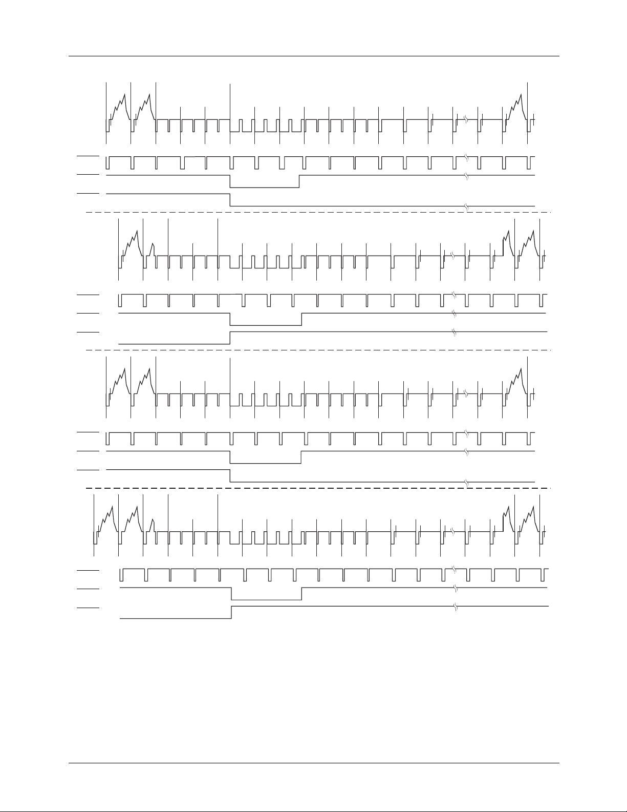
Figure 14. PAL-M Vertical Interval
-BB UBBUBB UBB UVV
271 279
UBB UBB UBB UBV UVV
•••
280 281
•••
65-6294-17
REV. 1.0.0 8/13/03 19
Page 20
TMC2192 PRODUCT SPECIFICATION
Table 10. PAL-M Field/Line Sequence and Identification
Field 1 & 5
FIELD ID = 000, 100
Field 2 & 6
FIELD ID = 001, 111
Field 3 & 7
FIELD ID = 010, 110
Field 4 & 8
FIELD ID = 011, 111
Line ID LTYPE Line ID LTYPE Line ID LTYPE Line ID LTYPE
1 SS 03 263 ES 01 1 SS 03 263 ES 01
2 SS 03 264 SS 03 2 SS 03 264 SS 03
3 SS 03 265 SS 03 3 SS 03 265 SS 03
4 EE 00 266 SE 02 4 EE 00 266 SE 02
5 EE 00 267 EE 00 5 EE 00 267 EE 00
6 EE 00 268 EE 00 6 EE 00 268 EE 00
7 -BB 05 269 EB 10 7 -BB 05 269 EB 10
8 -BB 05 270 -BB 05 8 UBB 05 270 UBB 05
9 UBB 0D 271 UBB 1D 9 UBB 0D 271 UBB 1D
………………………………
17 UBB 0D 279 UBB 0D 17 UBB 0D 279 UBB 0D
18 UVV 0F 280 UBV 0E. 18 UVV 0F 280 UBV 0E.
………281 UVV 0F … UVV 0F 281 UVV 0F
259 UVV 0F ………258 UVV 0F ………
260 -VE 04 521 UVV 0F 259 -VV 07 521 UVV 0F
261 EE 00 522 -VV 07 260 -VE 04 522 UVV 0F
262 EE 00 523 EE 00. 261 EE 00 523 EE 00
524 EE 00 262 EE 00 524 EE 00
525 EE 00 525 EE 00
EE Equalization pulse
SE Half-line vertical sync pulse, half-line equalization pulse
SS Vertical sync pulse
ES Half-line equalization pulse, half-line vertical sync pulse
EB Equalization broad pulse
UBB Black burst
-BB Black burst with color burst suppressed
UVV Active video
-VV Active video with color burst suppressed
UVE Half-line video, half-line equalization pulse
-VE Half-line video, half-line equalization pulse, color burst suppressed.
UBV half-line black, half-line video
20 REV. 1.0.0 8/13/03
Page 21
PRODUCT SPECIFICATION TMC2192
Chrominance Processor
Control registers for this section:
Address Bit(s) Name
0x06 7-6 FORMAT
0x06 5-3 MODE
0x07 5 DDSRST
0x11 7 DRSSEL
0x18 6 GLKCTL1
0x18 5 GLKCTL0
0x3F 3 GAUSS_BYP
0x40 7-0 FREQL
0x41 7-0 FREQ3
0x42 7-0 FREQ2
0x43 7-0 FREQM
0x44 7-4 SYSPHL
0x45 3-0 SYSPHM
0x46 7-4 BURPHL
0x47 3-0 BURPHM
0x48 7-4 BRSTFULL
0x49 3-0 BRST1
0x4A 7-4 BRST2
Subcarrier Programming
The color subcarrier is produced by an internal 32 bit digital
frequency synthesizer which is completely programmable in
frequency and phase. Separate registers, FREQx, SYSPHx,
BSTPHx, are provided for phase adjustment of the color
burst and of the active video, permitting external delay compensation, color adjustment, etc. FREQx is the subcarrier
phase step per pixel and SYSPHx is phase offset at field 1,
line 1 (line 4 for NTSC), pixel 1.
NTSC Subcarrier
For NTSC encoding, the subcarrier synthesizer frequency
has a simple relationship to the pixel clock period, repeating
over 2 lines: The decimal value for the subcarrier phase step
is:
455 2⁄
FREQx
Where the number of pixels/line is:
pixels line⁄
This value must be converted to binary and split into four 8
bit registers, FREQM, FREQ2, FREQ3, and FREQL.
PAL Subcarrier
The PAL relationship is more complex, repeating only once
in 8 fields (the well-known 25 Hz offset):
FREQx
This value must be converted to binary and split as described
previously for NTSC. The number of pixels/line is found as
in NTSC.
PAL-M Subcarrier
FREQ
SYSPHx establishes the appropriate phase relationship
between the internal synthesizer and the chroma modulator.
The nominal value for SYSPHx is zero.
Other values for SYSPHx must be converted to binary and
split into two 8 bit registers, SYSPHM and SYSPHL.
Burst Phase (BURPHx) sets up the correct relative NTSC
modulation angle. The value for BURPH is:
--------------------------pixels line⁄
PXCK Frequency
------------------------------------------=
1135 4⁄()1 625⁄()+
--------------------------------------------------pixels line⁄
909 4⁄
--------------------------pixels line⁄
232×=
H Period
232×=
32
×=
2
BURPHx = SYSPHx
This value must be converted to binary and split into two 8
bit registers, BURPHM and BURPHL.
REV. 1.0.0 8/13/03 21
Page 22
TMC2192 PRODUCT SPECIFICATION
Table 11. Standard Subcarrier Parameters
Field
Horizontal
Standard
NTSC sqr. pixel 59.94 15.734266 12.27 24.54 3.57954500 00 00 00 00 4A AA AA AB
NTSC CCIR-601 59.94 15.734266 13.50 27.00 3.57954500 00 00 00 00 43 E0 F8 3E
NTSC 4x F
PAL sqr. pixel 50.00 15.625000 14.75 29.50 4.43361875 00 00 00 00 4C F3 18 19
PAL CCIR-601 50.00 15.625000 13.50 27.00 4.43361875 00 00 00 00 54 13 15 96
PAL 15 Mpps 50.00 15.625000 15.00 30.00 4.43361875 00 00 00 00 4B AA C6 A1
PAL-M sqr.pixel 60.00 15.750000 12.50 25.01 3.57561149 00 00 00 00 49 45 00 51
PAL-M CCIR-601 60.00 15,750000 13.50 27.00 3.57561149 00 00 00 00 43 DF 3F D7
PAL-M 4x F
Subcarrier Synchronization
SC
Rate
(Hz)
59.94 15.734266 14.32 28.64 3.57954500 00 00 00 00 40 00 00 00
60.00 15,750000 14.30 28.60 3.57561149 00 00 00 00 40 10 66 F5
SC
Freq.
(kHz)
There are 5 modes of subcarrier synchronization in the
TMC2192, freerun, subcarrier reset, Genlock, DRS-lock and
Ancillary Data Control (ANC).
• Freerun
At the rising edge of RESET the DDS starts to generate the
subcarrier reference and will continue to freerun the subcarrier. When setting the control register DDSRST is HIGH, the
TMC2192 will reset the DDS to the SYSPH value on the
next field 1, line 1 (line 4 for NTSC), pixel 1 occurrence and
will reset this bit to be LOW. This allows the encoder to start
with the correct SCH relationship. The phase of the subcar-
Pixel
Rate
(Mpps)
PXCK
Freq.
(MHz)
Subcarrier
Freq.
(MHz)
BURPHM BURPHL SYSPHM SYSPHL FREQM FREQ2 FREQ3 FREQL
47 46 45 44 43 42 41 40
the TMC22x5y. The TMC22x5y produces a decoder reference signal (DRS) which contains field identification, PALODD status, relative phase and relative frequency of the
composite or S-video input. The DRS is sampled on either
the CVBS bus or the PD port, depending on DRSSEL, 60
PXCK’s after the falling edge of HSIN. The phase and frequency values are used to update the DDS on a line to line
basis, thus synchronizing the subcarrier to an external composite reference.
• Ancillary Data Control (ANC)
Subcarrier synchronization in ANC mode is covered in the
Ancillary Data Control section of this data sheet.
Subcarrier Register (hex)
rier reference will drift over time since a 32 bit accumulator
has a error of ±0.5 Hz when generating the subcarrier reference for NTSC 13.5 MHz.
SCH Phase Error Correction
SCH refers to the timing relationship between the 50% point
of the leading edge of horizontal sync and the positive or
• Subcarrier Reset
negative zero-crossing of the color burst subcarrier reference. SCH error is usually expressed in degrees of subcarrier
At the rising edge of RESET the DDS starts to generate the
subcarrier reference and will reset the DDS to the SYSPH
value every field 1, line 1 (line 4 for NTSC), pixel 1 occurrence. This enables the encoder to maintain the proper SCH
relationship.
• Genlock
The Genlock mode allows the TMC2192 to lock to a composite reference when used in conjunction with the
TMC22071A Genlocking Video Digitizer. The TMC22071A
produces a genlock reference signal (GRS) which contains
field identification, PALODD status, relative phase and relative frequency of the composite reference. The GRS is sampled on the CVBS bus 60 PXCK’s after the falling edge of
HSIN. The phase and frequency values are used to update
the DDS on a line to line basis, thus synchronizing the subcarrier to an external composite reference.
• DRS-Lock
phase. In PAL, SCH is defined for line 1 of field 1, but since
there is no color burst on line 1, SCH is usually measured at
line 7 of field 1. The need to specify SCH relative to a particular line in PAL is due to the 25 Hz offset of PAL subcarrier
frequency. Since NTSC has no such 25 Hz offset, SCH
applies to all lines.
The SCH relationship is important in the TMC2192 when
two video sources are being combined or if the composite
video output is externally combined with another video
source. In these cases, improper SCH phasing will result in a
noticeable horizontal jump of one image with respect to
another and/or a change in hue proportional to the SCH error
between the two sources.
SCH phasing can be adjusted by modifying BURPH and
SYSPH values by equal amounts. SCH is advanced/delayed
by one degree by increasing/decreasing the value of BURPH
and SYSPH by approximately B6h. An SCH error of 15o is
corrected with SYSPH and BURPH offsets of AAAh.
The DRS-Lock mode allows the TMC2192 to lock its composite output to the decoded composite or S-video input of
22 REV. 1.0.0 8/13/03
Page 23
PRODUCT SPECIFICATION TMC2192
Burst Envelope
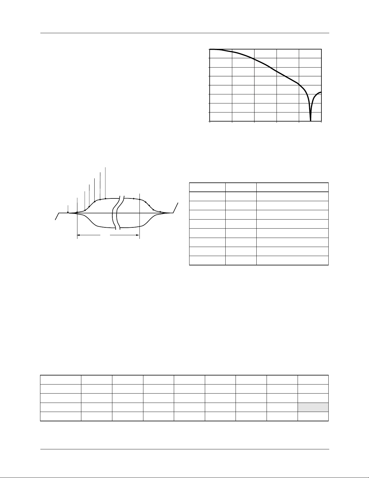
The TMC2192 includes the ability to adjust the burst amplitude and the shape of the burst. The Control Registers
BRSTFULL, BRST1 and BRST2 hold the magnitude of the
burst vector. BRSTFULL is the maximum amplitude of the
burst vector. BRST1 and BRST2 determine the intermediate
values of the burst vector for the burst envelope shaping. A 5
pixel burst envelope shaping occurs at the rising and falling
edges of burst. At the rising edge of burst the next 5 pixels
have the following weighting; BRSTFULL – BRST1,
BRSTFULL – BRST2, BRSTFULL/2, BRST2, and BRST1.
At the falling edge of burst the next 5 pixels have the following weighting; BRST1, BRST2, BRSTFULL/2, BRSTFULL
– BRST2, and BRSTFULL – BRST1. With this flexibility
the user determine the shape, amplitude and width of the
burst signal.
BRSTFULL
BRST1
BRSTFULL/2
BRSTFULL - BRST2
BRSTFULL - BRST1
BLANK
Color-Difference Low-Pass Filters
BRST2
BU
Figure 15. Burst Envelope
65-6294-18
The chrominance portion of a composite video signal must
be sufficiently bandlimited to avoid cross-color and crossluminance distortion, and to preclude exceeding the allowable bandwidth of a video channel.
The color-difference low-pass filters on the TMC2192
establish chrominance bandwidths which meet the specifications outlined in CCIR Report 624-3, Table II, Item 2.6, for
system I over a range of pixel rates from 12.27 Mpps to
14.75 Mpps. Equal bandwidth is established for both colordifference channels.
0
-10
-20
-30
-40
-50
Attenuation (db)
-60
-70
-80
0 0.1 0.2 0.3 0.4 0.5
Normalized Frequency (Pixel rate)
Figure 16. Gaussian Filter Response
Sync and Pedestal Insertion
Control Registers for this section
Address Bit(s) Name
0x06 7-6 MODE
0x11 5 COMP2DB
0x14 7-0 VBIPEDEM
0x15 7-0 VBIPEDEL
0x16 7-0 VBIPEDOM
0x17 7-0 VBIPENOL
0x1A 6-0 PEDHGT1
0x3F 3 C2DB_OFF
Pedestal Enable
The TMC2192 has the ability to independently select lines
for pedestal insertion during the vertical blanking interval
(VBI). For 525-line systems and using the NTSC line numbering convention, in which the first vertical serration is on
line 4 for field 1 and line 266 for field 2, the vertical interval
lines map to the control registers VBIPEDxy as shown in
Table 15.
65-6294-19
Table 12. Line by Line Pedestal Enable
Bit 76543210
VBIPEDEL 17 16 15 14 13 12 11 10
VBIPEDEM 25* 24 23 22 21 20 19 18
VBIPEDOL 279 278 277 276 275 274 273
VBIPEDOM 287* 286 285 284 283 282 281 280
REV. 1.0.0 8/13/03 23
Page 24
TMC2192 PRODUCT SPECIFICATION
Enabling the pedestal on line 25 enables it for the remainder
of field 1, to line 262. Likewise, enabling the pedestal on line
288 enables it for the remainder of field 2.
Pedestal Height
PEDHGT1 determines the height of the pedestal for the
luminance channel on the composite path. The range of the
pedestal height is from -22.1 to 21.74 IRE in .345 IRE increments.
Sync and Blank Insertion
The composite paths blank and sync D/A codes are determined by the FORMAT control register. For NTSC and
PAL-M formats the blank D/A code is 240 (295 mV) and the
sync D/A code is 8 (9 mV). For all other PAL formats the
blank D/A code is 256 (314 mV) and the sync D/A code is
12 (14 mV).
In all cases the sync edges are sloped to insure the proper rise
and fall times in all video standards.
Closed Caption Insertion
Control Registers for this section
Address Bit(s) Name
0x1C 7-6 CCD1
0x1D 1-0 CCD2
0x1E 7 CCON
0x1E 6 CCRTS
0x1E 5 CCPAR
0x1E 4 CCFLD
0x1E 3–0 CCLINE
Line Selection
The line to contain CC data is selected by a combination of
the CCFLD bit and the CCLINE bits. CCLINE is added to
the offset shown in Table 16 to specify the line.
Table 13. Closed Caption Line Selection
Standard Offset Field Lines
525 12 ODD 12-27
274 EVEN 274-289
625 16 ODD 16-31
328 EVEN 328-343
Parity Generation
Standard Closed-Caption signals employ ODD parity, which
may be automatically generated by setting CCPAR HIGH.
Alternatively, parity may be generated externally as part of
the bytes to be transmitted, and, with CCPAR LOW, the
entire 16 bits loaded into the CCDx registers will be sent
unchanged.
Operating Sequence
A typical operational sequence for closed-caption insertion
on line xx is:
Read Register 1E and check that bit 7 is LOW, indicating that the CCDx registers are ready to accept data.
If ready, write two bytes of CC data into registers 1C
and 1D.
Write into register 1E the proper combination of
CCFLD and CCLINE. CCPAR may be written as
desired. Set CCRTS HIGH.
The CC data is transmitted during the specified line.
The TMC2192 includes a flexible closed-caption processor.
It may be programmed to insert a closed caption signal on
any line within a range of 16 lines on ODD and/or EVEN
fields. Closed Caption insertion overrides all other configurations of the encoder: if it is specified on an active video line,
it takes precedence over the video data and removes NTSC
setup if setup has been programmed for the active video
lines. Closed Caption is only available when the TMC2192
is in a 13.5 MHz pixel rate.
Closed caption is turned on by setting CCON HIGH. Whenever the encoder begins producing a line specified by
CCFLD and CCLINE, it will insert a closed caption line in
its place. If CCRTS is HIGH, the data contained in CCDx
will be sent. IF CCRTS is LOW, Null bytes (hex 00 with
ODD parity) will be sent.
24 REV. 1.0.0 8/13/03
As soon as CCDx s transferred into the CC processor (and
CCRTS goes LOW), new data may be loaded into registers
1C and 1D. This allows the user to transmit CC data on several consecutive lines by loading data for line n+1 while data
is being sent on line n.
Page 25
PRODUCT SPECIFICATION TMC2192
Interpolation Filters
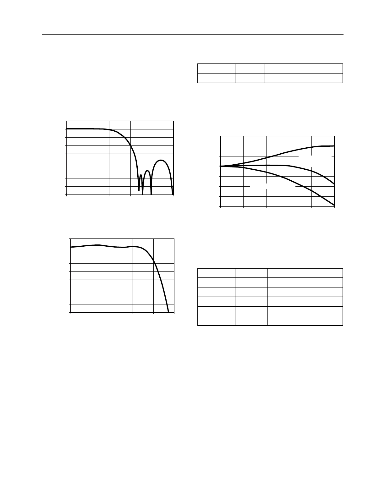
Each video output on the TMC2192 is digitally filtered with
sharp-cutoff low-pass interpolation filters. These filters
ensure that the frequency band above base-band video and
below the pixel frequency (f
PXCK frequency) are sufficiently suppressed.
Since these are fixed-coefficient digital filters, their filter
characteristics depend upon clock rate.
10
0
-10
-20
-30
-40
-50
Attenuation (db)
-60
-70
-80
0 0.2 0.4 0.6 0.8 1
Figure 17. Interpolation Filter
0.5
0
-0.5
-1
-1.5
-2
-2.5
Attenuation (db)
-3
-3.5
-4
0 0.1 0.2 0.3 0.4 0.5
Figure 18. Interpolation Filter – Passband Detail
/4 to 3fS/4, where fS is the
S
Frequency (Pixel rate)
Frequency (Pixel rate)
65-6294-21
65-6294-20
x/Sin(x) Filter
Control Registers for this section
Address Bit(s) Name
0x11 4 SINEN
The TMC2192 contains a selectable X/sin(X) filter prior to
each DAC. The X/sin(X) filter boosts the high frequency
data to negate the sin(X)/X roll-off associated with D/A converters.
1.5
1
0.5
0
-0.5
-1
Attenuation (db)
-1.5
-2
0 0.1 0.2 0.3 0.4 0.5
Normalized Frequency (PXCK)
Figure 19. X/SIN(X) Filter
X/Sin(x) Filter
Compensated
D/A Output
Sin(x)/x D/A Roll-Off
Output Data Formats
Control Registers for this section
Address Bit(s) Name
0x10 5 LUMADIS
0x10 6 CHROMADIS
0x10 7 COMPDIS
0x3F 7 SEL_CLK
0x3F 4 SEL_PIX
65-6294-22
REV. 1.0.0 8/13/03 25
Page 26
TMC2192 PRODUCT SPECIFICATION
Analog outputs of the TMC2192 are driven by three 10 bit
D/A converters, operating at twice the pixel rate. The outputs
drive standard video levels into 37.5 or 75 Ohm loads. An
internal voltage reference is used to provide reference current for the D/A converters. For more accurate levels, an
external fixed or variable voltage reference source is accommodated. The video signal levels from the TMC2192 may be
adjusted by varying the common Vref or the 3 independent
Rrefs. Each video D/A converter has an independent reference resistor that can adjust the output gain. D/A Matching
Ancillary Data
Control Registers for this section
Address Bit(s) Name
0x07 2 ANCFREN
0x07 1 ANCPHEN
0x07 0 ANCTREN
0x08 7-0 ANCID
is achieved by trimming the each external reference resistor
of each D/A.
The TMC2192 is designed to accept 15 words of ancillary
data after the active video pixels at the end of each horizontal
Digital Composite Output
In addition, the TMC2192 supplies a 10 bit digital composite
signal on pins D[7:0] and FLD[2:1]. The digital composite
output can be either an interpolated signal on a non-interpo-
line. Ancillary data may occur once per line, once per field,
once per eight fields, on random lines, or not al all. The
TMC2192 does not assume ancillary data is present on a reg-
ular basis.
lated signal, this controlled by the control register
SEL_CLK.
Table 14. Ancillary Data Format
Word ID Description B
ANC2 Ancillary Data Header (Timing
ANC1 11111111
Reference Signal)
00000000
B
7
B
6
B
5
B
4
B
3
B
2
1
ANC0 11111111
TT Data Type TT6 TT5 TT4 TT3 TT2 TT1 TT0 P
MM Word 0 D11 D10 D9 D8 D7 D6 P
LL Count 0 D5 D4 D3 D2 D1 D0 P
FIELD Field ID/Synchronous Video Flag x x x SVF F2 F1 F0 P
reserved xxxxxxxP
PH1 Subcarrier Phase PHV PH
PH0 PH
PH
6
FR4 Subcarrier Frequency FRV x x FR
FR3 FR
FR2 FR
FR1 FR
FR0 FR
Note:
1. P = odd parity bit, x = reserved bit will be ignored
27
20
13
FR
FR
FR
FR
6
12
26
19
12
PH
PH
5
FR
FR
FR
FR
5
11
25
18
11
PH
PH
4
FR
FR
FR
FR
4
10
31
24
17
10
PH
PH
3
FR
FR
FR
FR
FR
3
30
23
16
PH
9
PH
2
FR
FR
FR
FR
9
FR
2
29
22
15
PH
8
1
8
1
PH
FR
FR
FR
FR
FR
7
0
28
21
14
7
0
B
0
P
P
P
P
P
P
P
The first three words of ancillary data comprise the TRS signal (ANC2-0) which indicates the end of active video. Also
The word count data (D
in MM, LL) in the ancillary data
11-0
packet indicate the number of words in ancillary data.
known as the Ancillary data header, the TRS signal is a 00h,
FFh, FFh sequence. Except for the TRS words, ancillary data
bit 0 (B0, LSB) is odd parity for B
7-1
.
The data type word (TT) is used to specify the ancillary data
Ancillary phase data is used to program the MSBs of the
PHASE register. ANCPHEN and PHV determine how ancil-
lary phase data is used. When ancillary data is not present,
the TMC2192 assumes PHV = LOW.
type. The TMC2192 compares this 7 bit value with the contents of the ANCID control register. If there is a match, the
ancillary data will be processed. If there is no match, the
TMC2192 ignores ancillary data.
26 REV. 1.0.0 8/13/03
Page 27
PRODUCT SPECIFICATION TMC2192
Table 15. Ancillary Data Control – Phase
ANCPHEN PHV Description
0 x Ignore ancillary phase data,
set PHASE = 0
1 0 Ignore ancillary phase data,
no change to PHASE
1 1 Load ancillary phase data into
PHASE registers
Ancillary frequency data is used to program the 32 bits of the
ancillary frequency data is used. When ancillary data is not
present, the TMC2192 assumes FRV = LOW.
Table 16. Ancillary Data Control Frequency
ANCFREN FRV Description
0 x Ignore ancillary frequency
1 0 Ignore ancillary frequency
1 1 Load ancillary frequency data
FREQ3-0 registers. ANCFREN and FRV determine how
Table 17. Field Identification and Subcarrier Reset Modes
ANCTREN SVF F
2
F
1
F
F (EAV) Field ID / Subcarrier Reset Mode
0
Basic Mode
0 xxxx 0Odd field, reset subcarrier every 8 fields
0 xxxx 1Even field
Genlocking Mode
1 1 x x x 0 Odd field, subcarrier free run
1 1xxx 1Even field
Field Sequence Mode
1 0000 0Field 1, reset subcarrier at field 1
1 0001 1Field 2
1 0010 0Field 3
1 0011 1Field 4
1 0100 0Field 5
1 0101 1Field 6
1 0110 0Field 7
1 0111 1Field 8
Note:
1. The F bit is part of the EAV timing reference code and tracks the F0 bit.
data
data
into FREQ3-0 registers
Operating Modes
The field number bits (F
) from the ancillary data packet
2-0
FIELD word, are used to program the encoder’s field counter
depending upon the state of the synchronous video flag
(SVF) and the ANCTREN bit in the control register.
In the basic operating mode (ANCTREN = LOW), all timing
is found in the F bit of EAV. F
and SVF are ignored and
2-0
the encoder subcarrier synthesizer is reset to the PHASE
value every eight fields (when the field counter transitions
from 111 (field 8) to 000 (field 1).
In the basic mode, ANCFREN and ANCPHEN are typically
set LOW, ignoring ancillary frequency and phase data. If
ANCFREN and ANCPHEN are HIGH, the TMC2192 uses
the incoming ancillary frequency and phase data on a line-
In genlocking mode (ANCTREN and SVF = HIGH), the
subcarrier synthesizer is allowed to free run, with phase and
frequency being set from the ancillary data packet PH
and FR
data. The field counter increments just like it
31-0
12-0
does in basic mode.
Field sequence mode (ANCTREN = HIGH and SVF =
LOW), is the same as basic mode except that the field
counter is set by the F
bits in the FIELD word of ancillary
2-0
data. If ancillary data is not present on a line, the field
counter will continue to count as it does in basic mode.
When ancillary data is present, the contents of the field
counter are loaded with field data (F
). In this way, the
2-0
TMC2192 may be synchronized with an external source by
sending field data only once.
by-line basis.
REV. 1.0.0 8/13/03 27
Page 28
TMC2192 PRODUCT SPECIFICATION
Layering Engine
Control Registers for this section
Address Bit(s) Name
0x04 2 SKEN
0x05 3-2 OMIX
0x07 6 SKFLIP
0x09 7 HKEN
0x09 6 BUKEN
0x09 5 SKEXT
0x09 4 DKDIS
0x09 3 EKDIS
0x09 2 FKDIS
0x09 1-0 LAYMODE
Table 18. Layering and Keying Modes
LAYMODE BACKGROUND MIDGROUND FOREGROUND
Image Source Image Source Keying Control Image Source Keying Control
0 PD OVERLAY OL4-0 CVBS KEY or Data Key
1 PD CVBS KEY or Data Key OVERLAY OL4-0
2 CVBS OVERLAY OL4-0 PD KEY or Data Key
3 CVBS PD KEY or Data Key OVERLAY OL4-0
Address Bit(s) Name
0x0A 7-0 DKEYMAX
0x0B 7-0 DKEYMIN
0x0C 7-0 EKEYMAX
0x0D 7-0 EKEYMIN
0x0E 7-0 FKEYMAX
0x0F 7-0 FKEYMIN
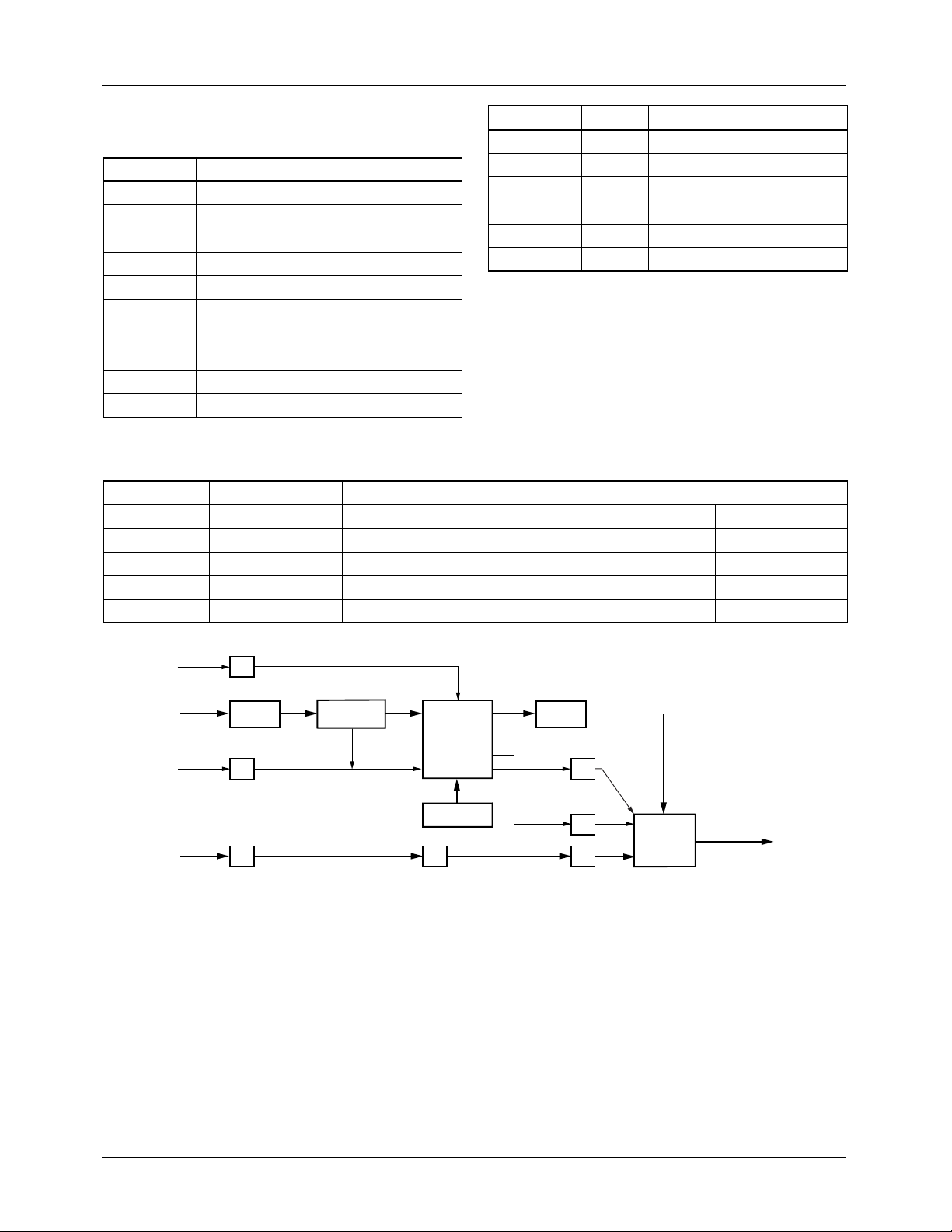
The TMC2192 features a robust layering engine with three
possible input layers controlled by two keying controls. The
layer assignments are shown in Table 22, along with the key-
ing control. The keying controls, KEY pin or OL4-0 are
aligned with the incoming pixel data stream and are then
delayed throughout the chip to be continuously aligned with
the input video streams. A generic overview of the keying
and layering features is shown in Figure 21.
OL4-0
PD
KEY
CVBS
Overlay Mixer
dT
LOGIC LOGIC
dT
dT dT dT
DATA KE Y
OVERLAY
MIXER
OLUT
Figure 20. Layering Engine
The OL[4:0] bus provides the ability to overlay 30 different
24 bit values onto the pixel data path. The 24 bit overlay colors must be the same format as the incoming Pixel data. For
Y,Cb,Cr input formats the range of Y values spans the entire
range of the format, 1 to 254, this enables super whites and
super blacks in the overlay palette.
When OL[4:0] is equal to 00h the pixel data port to be the
output of the overlay mixer. If OL[4:0] is in the range of 1 to
31 then the output source is one of 30 possible overlay col-
PD
1/2AMP
dT
dT
YC
KEYING
MIXER
COMP
65-6294-23
ors, see Table 22. Overlay Address Map. When OL4-0 equal
to 16, the overlay mixer produces a pixel data output with
half the luminance magnitude and chrominance magnitude.
Any OL4-0 value greater than 16 will result in a overlay mix
with a full amplitude overlay and the pixel data with half
amplitude pixel data (PD) or half amplitude CVBS data as its
values. This allows for transparent overlays or produce
shadow boxes around overlaid text.
The midpoint of the rising and falling edges on the mixed
output is determined by the transition of the OL[4:0] pins in
28 REV. 1.0.0 8/13/03
Page 29
PRODUCT SPECIFICATION TMC2192
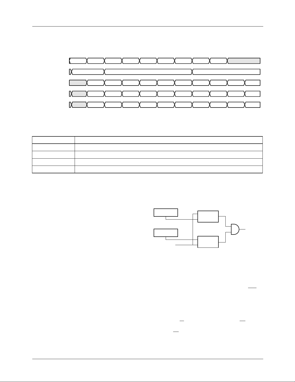
relation to the PD port. Control register OMIX chooses
among the following set of coefficients; either 0 1/8 1/2 7/8
lay color. The timing diagram in Figure 22 identifies the
three possible output formats that the mixer can produce.
1, 0 1/2 1 , or 0 1 to switch between the PD port and the over-
PDx
MixOUT (OMIX = 3)
MixOUT (OMIX = 2)
MixOUT (OMIX = 1)
A
BCDEFGH I
A>0 0OL[4:0]
A 7/8B, 1/8OL 1/2C, 1/2OL 1/8D, 7/8OL OL I1/8F, 7/8OL 1/2G, 1/2OL 7/8H, 1/8OL
AB1/2C, 1/2OL OL OL IOL 1/2G, 1/2OL H
A B OL OL OL IOL OL H
Figure 21. Overlay Outputs
Table 19. Overlay Address Map
OL4-0 Result
0 Pixel data is passed through overlay mixer.
1-15 Overlay is mixed with PD or CVBS at the transitions.
16 Half amplitude PD or half amplitude CVBS is the output of COMP2.
17-31 Overlay is mixed with half amplitude PD or half amplitude CVBS at the transitions.
65-6294-24
Hardware Keying
The KEY input switches the input to the Comp data path
between the composite video generated from the PD port and
the CVBS data bus on a pixel-by-pixel basis. This is a “soft”
switch is executed over 3 PCK periods to minimize out-ofband transients. Keying is accomplished in the digital composite video domain. The coefficients for the mix are 0, 1/8,
1/2, 7/8, and 1 . The COMP output is the final output for all
overlay functions.
Hardware keying is enabled by the key Control Register
HKEN. Normally, keying is only effective during the active
video portion of the encoded video line (as determined by
Control Register VA). That is, the horizontal blanking interval is generated by the encoder even if the KEY signal is
held HIGH through horizontal blanking. However, it is possible to allow digital horizontal blanking to be passed
through from the CVBS bus to the COMP output by setting
key Control Register BUKEN HIGH. In this mode, KEY is
always active, and may be exercised at will.
The KEY input is registered into the encoder just as Pixel
data is clocked into the PD port. It is internally pipelined, so
the midpoint of the KEY transition occurs at the output of
the pixel that was input at the same time at the KEY signal.
Data Keying
Data keying for each channel Y, Cb, and Cr, is separately
enabled or disabled by the control registers DKEYDIS,
EKEYDIS, and FKEYDIS. On each channel the eight (8)
MSBs of the pixel data are compared against a maximum
key value and a minimum key value. If the pixel data is
greater than xKEYMIN and less than or equal to xKEY-
MAX, then a key match is signaled for that channel.
xKEYMAX
xKEYMIN
xCHANNEL
Figure 22. Data Keying
A
A<=B
B
KEY
MATCH
A
A<=B
B
65-6294-25
By allowing a window of possible key values on each chan-
nel the TMC2192 opens a key cube in the color space.
Parallel Microprocessor Interface
The parallel microprocessor interface is active when SER is
HIGH and employs a 12-line interface; an 8 bit data bus and
2 bit address location, 1 bit read/write select, and a chip
select controlling the timing. Two addresses are required for
device programming, one to the pointer and one to the data
location. When writing, the address is presented along with a
LOW on the R/W pin during the falling edge of CS. Eight
bits of data are presented on D7-0 during the subsequent ris-
ing edge of CS.
REV. 1.0.0 8/13/03 29
Page 30
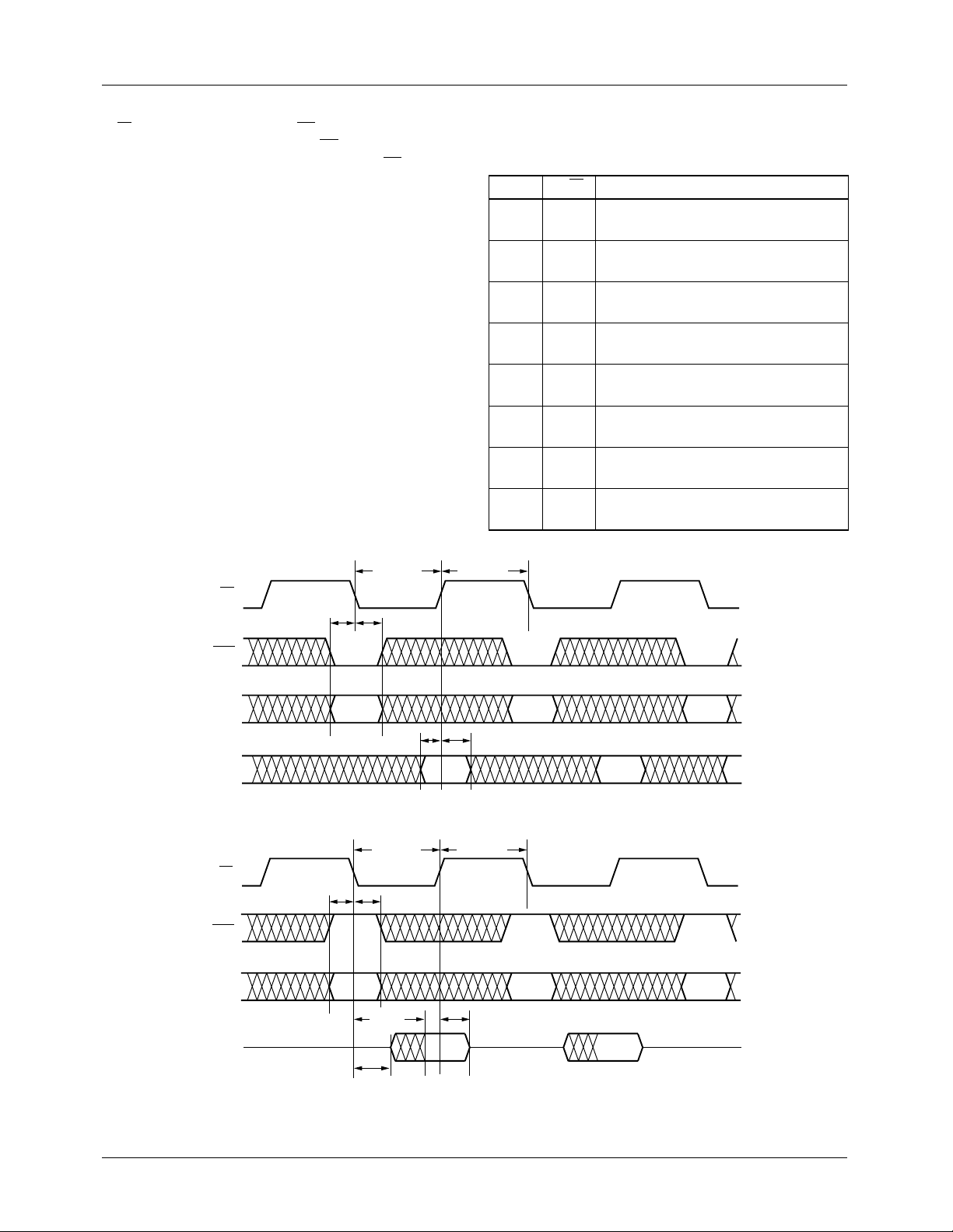
TMC2192 PRODUCT SPECIFICATION
In read mode, the address is accompanied by a HIGH on the
R/W pin during a falling edge of CS. The data output pins go
to a low-impedance state t
present on D7-0 t
after the falling edge of CS. Because
DOM
after CS falls. Valid data are
DOZ
this port operates asynchronously with the pixel timing,
there is an uncertainty in this data valid output delay of one
PXCK period. This uncertainty does not apply to t
DOZ
.
Writing data to specific control registers of the TMC2192
requires that the 8 bit address of the control register of interest be written prior to the data. This control register address
is the base address for subsequent write operations. The base
address auto increments by one for each byte of data written
after the data byte intended for the base address. If more
bytes are transferred than there are available addresses, the
address will not increment and remain at its maximum value
of 4Ch.
Writing data to specific OLUT location of the TMC2192
requires that the 8 bit address of the OLUT location of interest be written prior to the data sequence. This OLUT location address is the base address for subsequent write
operations. The base address auto increments by one for
each sequence of three (3) bytes of data written after the data
byte intended for the base address. The sequence of data
transfer is Y, C
, Cr , after the Cr byte is transferred the base
b
address will increment by one (1).
Table 20. Parallel Port Control
A
00 0 Load D
R/W Action
1-0
into Control Register
7-0
pointer (block 0)
00 1 Read Control Register pointer on
D
7-0
01 0 Load D
into addressed OLUT
7-0
Location pointer (block 0)
01 1 Read addressed OLUT Location
pointer on D
10 0 Write D
7-0
.
7-0
to addressed Control
Register
10 1 Read addressed Control Register
on D
7-0
11 0 Write D
to addressed OLUT
7-0
Location
11 1 Read addressed OLUT Location on
D
7-0
t
PWLCS
CS
R/W
ADR
D
7-0
CS
R/W
ADR
t
SA
Figure 23. Microprocessor Parallel Port – Write Timing
t
SA
t
HA
t
PWLCS
t
HA
t
DOM
t
SD
t
PWHCS
t
HD
t
PWHCS
t
HOM
65-6294-26
D
7-0
t
DOZ
Figure 24. Microprocessor Parallel Port – Read Timing
65-6294-27
30 REV. 1.0.0 8/13/03
Page 31
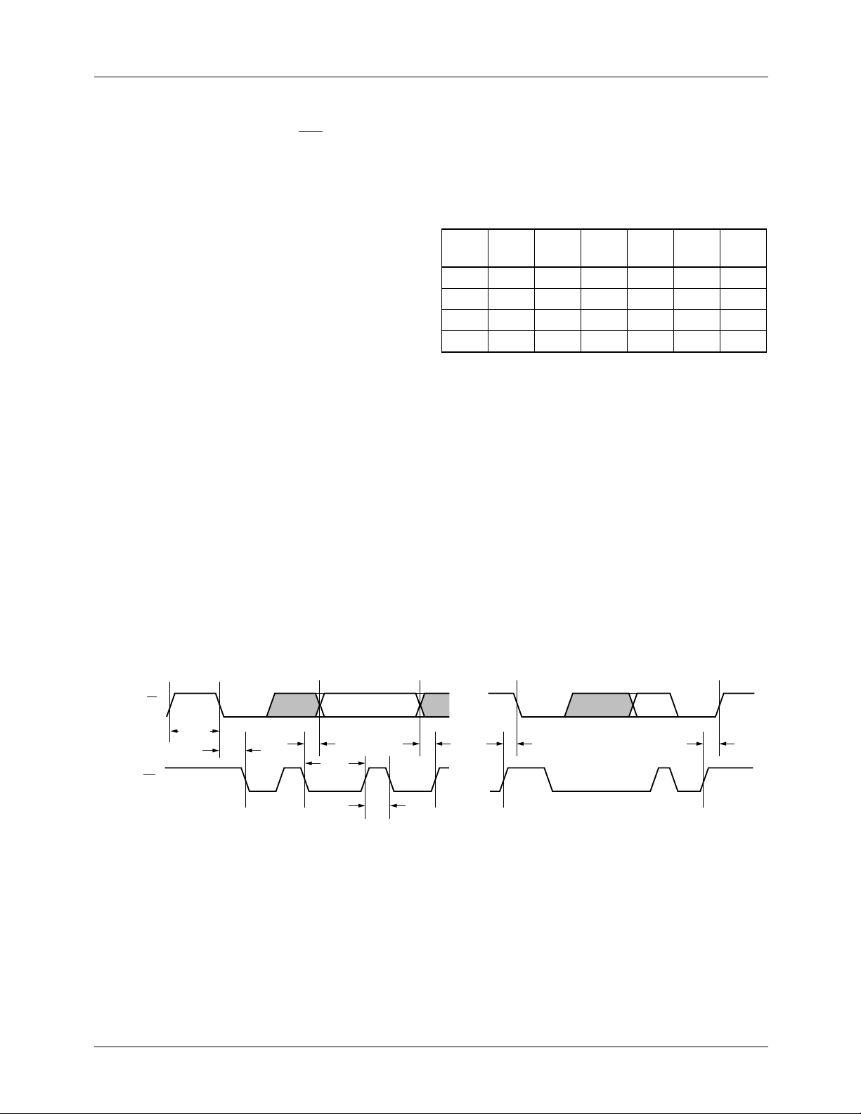
PRODUCT SPECIFICATION TMC2192
Serial Control Port (R-Bus)
In addition to the 12-wire parallel port, a 2-wire serial control interface is provided, active when SER is LOW. Either
port alone can control the entire chip. Up to four TMC2192
devices may be connected to the 2-wire serial interface with
each device having a unique address.
The 2-wire interface comprises a clock (SCL) and a bi-directional data (SDA) pin. The encoder acts as a slave for receiving and transmitting data over the serial interface. When the
serial interface is not active, the logic levels on SCL and
SDA need to be pulled HIGH by external pull-up resistors.
Data received or transmitted on the SDA line must be stable
for the duration of the positive-going SCL pulse. Data on
SDA must change only when SCL is LOW. If SDA changes
state while SCL is HIGH, the serial interface interprets that
action as a start or stop sequence.
There are six components to serial bus operation:
• Start signal
• Slave address byte
• Block Pointer
• Offset Pointer
• Data byte to read or write
• Stop signal
bit indicates the direction of data transfer, read from or write
to the slave device. If the transmitted slave address matches
the address of the device (set by the state of the SA1-0 input
pins in Table 24), the TMC2192 acknowledges by bringing
SDA LOW on the 9th SCL pulse. If the addresses do not
match, the TMC2192 will not acknowledge.
Table 21. Serial Port Addresses
A6 A5 A4 A3 A2A1(SA1)A0(SA0)
1010100
1010101
1010110
1010111
Data Transfer via Serial Interface
For each byte of data read or written, the MSB is the first bit
of the sequence.
If the TMC2192 does not acknowledge the master device
during a write sequence, the SDA remains HIGH so the mas-
ter can generate a stop signal. If the master device does not
acknowledge the TMC2192 during a read sequence, the
encoder interprets this as “end of data”.
When the serial interface is inactive (SCL and SDA are
HIGH) communications are initiated by sending a start signal. The start signal is a HIGH-to-LOW transition on SDA
while SCL is HIGH. This signal alerts all slaved devices that
a data transfer sequence is coming.
The first eight bits of data transferred after a start signal comprise a seven bit slave address and a single R/W bit. The R/W
SDA / R/W
t
SCL / CS
t
STAH
BUFF
t
DHO
t
DSU
t
DAL
Figure 25. Serial Port Read/Write Timing
Data are read from the control registers of the TMC2192 in a
similar manner. Reading requires two data transfer operations:
The base address must be written with the R/W bit of the
slave address byte LOW to set up a sequential read operation.
Writing data to specific control registers of the TMC2192
requires that the 8 bit address of the control register of inter-
est be written after the slave address has been established.
This control register address is the base address for subse-
quent write operations. The base address auto increments by
one for each byte of data written after the data byte intended
for the base address.
t
BAH
t
STASU
t
STOSU
Reading (the R/W bit of the slave address byte HIGH)
begins at the previously established base address. The
address of the read register auto increments after each byte is
transferred.
To terminate a write sequence to the TMC2192, a stop signal
must be sent. A stop signal comprises a LOW-to-HIGH tran-
sition of SDA while SCL is HIGH. To terminate a read
65-6294-28
REV. 1.0.0 8/13/03 31
Page 32
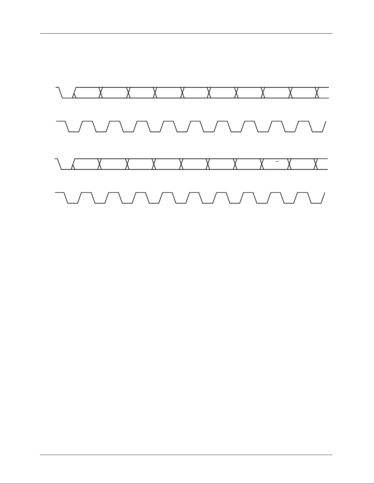
TMC2192 PRODUCT SPECIFICATION
sequence simply do not acknowledge (NOACK) the last byte
received and the TMC2192 will terminate the sequence.
A repeated start signal occurs when the master device driving the serial interface generates a start signal without first
SDA
SCL
SDA
SCL
Bit 7 Bit 6 Bit 5 Bit 4 Bit 3 Bit 2 Bit 1 Bit 0 ACK
Figure 26. Serial Interface – Typical Byte Transfer
A
6
A
5
A
4
Figure 27. Serial Interface – Chip Address
A
3
generating a stop signal to terminate the current communica-
tion. This is used to change the mode of communication
(read, write) between the slave and master without releasing
the serial interface lines.
65-6294-29
A
2
SA
1
SA
0
R/W ACK
65-6294-30
Serial Interface Read/Write Examples
Write to one control register
• Start signal
• Slave Address byte (R/W bit = LOW)
• Block Pointer (00)
• Offset Pointer
• Data byte to base address
• Stop signal
Write to four consecutive control registers
• Start signal
• Slave Address byte (R/W bit = LOW)
• Block Pointer (00)
• Offset Pointer
• Data byte to base address
• Data byte to (base address + 1)
• Data byte to (base address + 2)
• Data byte to (base address + 3)
• Stop signal
Write to one OLUT location
• Start signal
• Slave Address byte (R/W bit = LOW)
• Block Pointer (01)
• Offset Pointer (base address)
• Data byte to base address (Y)
• Data byte to base address (Cb)
• Data byte to base address (Cr)
• Stop signal
Write to four consecutive OLUT locations
• Start signal
• Slave Address byte (R/W bit = LOW)
• Block Pointer (01)
• Offset Pointer (base address)
• Data byte to base address (Y)
• Data byte to base address (Cb)
• Data byte to base address (Cr)
• Data byte to base address +1 (Y)
• Data byte to base address +1 (Cb)
• Data byte to base address +1 (Cr)
• Data byte to base address +2 (Y)
• Data byte to base address +2 (Cb)
• Data byte to base address +2 (Cr)
• Data byte to base address +3 (Y)
• Data byte to base address +3 (Cb)
• Data byte to base address +3 (Cr)
• Stop signal
Read from one control register
• Start signal
• Slave Address byte (R/W bit = LOW)
• Block Pointer (00)
• Offset Pointer
• Stop signal
• Start signal
• Slave Address byte (R/W bit = HIGH)
• Data byte from base address
•NOACK
32 REV. 1.0.0 8/13/03
Page 33
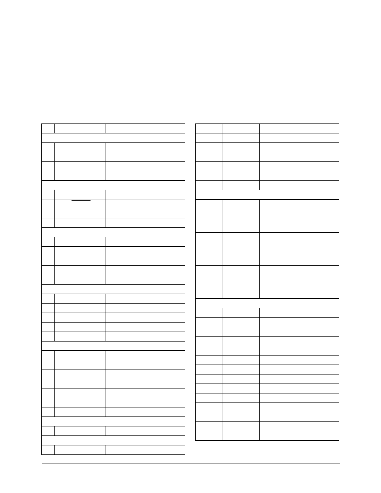
PRODUCT SPECIFICATION TMC2192
Read from four consecutive control registers
• Start signal
• Slave Address byte (R/W bit = LOW)
• Block Pointer (00)
• Offset Pointer
• Stop signal
• Start signal
Control Register Map
Table 22. Control Register Map
Reg Bit Mnemonic Function
TMC2192 Identification Registers (Read only)
00 7-0 PARTID2 Reads back 97h
01 7-0 PARTID1 Reads back 21h
02 7-0 PARTID0 Reads back 92h
03 7-0 REVID Silicon revision #
Gamma Filters Register
04 7-4 Reserved Set to Low
04 3 SRESET Software RESET
04 2 SKEN Data KEY Enable
04 1-0 PDRM Pixel Data Ramping Mode
Input Format Register
05 7 D1OFF YCBCR Input Formatting
05 6 Reserved Program Low
05 5-4 INMODE Input Mode Select
05 3-2 OMIX Overlay Mixer Select
05 1-0 SOURCE Video Input Select
General Control Register
06 7-6 FORMAT Video Format
06 5-3 MODE Video Mode
06 2 PDCDIR PDC Directional Control
06 1 TOUT External Sync Output Control
06 0 TSOUT External Sync Delay Control
Horizontal Ancillary Data Control Register
07 7 LDFID Field Lock Select
07 6 SKFLIP Soft Key Inversion
07 5 DDSRST DDS Reset
07 4-3 Reserved
07 2 ANCFREN Ancillary Frequency Enable
07 1 ANCPHEN Ancillary Phase Enable
07 0 ANCTREN Ancillary Timing Enable
Ancillary Data ID Register
08 7-0 ANCID Ancillary Data Identification
Keying/Overlay Engine
09 7 HKEN Hardware KEY Enable
• Slave Address byte (R/W bit = HIGH)
• Data byte from base address
• Data byte from (base address + 1)
• Data byte from (base address + 2)
• Data byte from (base address + 3)
•NOACK
Table 22. Control Register Map (continued)
Reg Bit Mnemonic Function
09 6 BUKEN Burst KEY Enable
09 5 SKEXT Data KEY Operation Select
09 4 DKDIS Green/Y Data KEY Disable
09 3 EKDIS Blue/C
09 2 FKDIS Red/CR Data KEY Disable
09 1-0 LAYMODE Layer Assignment Select
Key Value Registers
0A 7-0 DKEYMAX Green/Y Maximum Data Key
0B 7-0 DKEYMIN Green/Y Minimum Data Key
0C 7-0 EKEYMAX Blue/C
0D 7-0 EKEYMIN Blue/CB Minimum Data Key
0E 7-0 FKEYMAX Red/CR Maximum Data Key
0F 7-0 FKEYMIN Red/CR Minimum Data Key
DAC Control Registers
10 7 COMPDIS D/A #4 Disable
10 6 CHROMADIS D/A #3 Disable
10 5 LUMADIS D/A #2 Disable
10 4-3 Reserved Set to 0.
10 2 OLUTDIS Overlay LUT Disable
10 1-0 Reserved Program Low
11 7 DRSSEL DRS Selection
11 6 Reserved Program Low
11 5 COMP2DB Composite 2 Overflow Control
11 4 SINEN X/Sin(x) Filter Enable
11 3 Reserved Program Low
11 2 LUMDIS Luma Disable
11 1 CHRMDIS Chroma Disable
11 0 BURSTDIS Burst Disable
Data KEY Disable
B
Value
Value
Maximum Data Key
B
Value
Value
Value
Value
REV. 1.0.0 8/13/03 33
Page 34
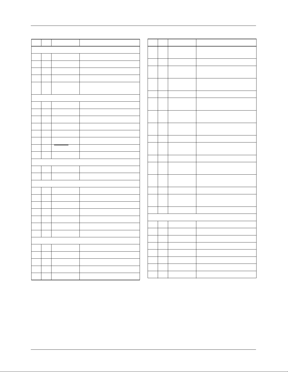
TMC2192 PRODUCT SPECIFICATION
Table 22. Control Register Map (continued)
Reg Bit Mnemonic Function
VBI Ped Enable Registers
14 7-0 VBIPEDEM VBI Pedestal Enable, Even Fields
15 7-0 VBIPEDEL VBI Pedestal Enable, Even Fields
16 7-0 VBIPEDOM VBI Pedestal Enable, Odd Fields
17 7-1 VBIPEDOL VBI Pedestal Enable, Odd Fields
17 0 HVA Horizontal and Vertical Sync
Alignment
Vertical Blanking Interval Enable Registers
18 7 Reserved Program Low
18 6 GLKCTL1 Genlock Control Register 1
18 5 GLKCTL0 Genlock Control Register 0
18 4-0 VBIENF1 VBI Active Video Enable, Field 1
19 7 SHORT Test Register
19 6 T512 EH/SL Offset Control Bit
19 5 HALFEN
19 4-0 VBIENF2 VBI Active Video Enable, Field 2
Pedestal Height Register
1A 7 Reserved Program Low
1A 6-0 PEDHGT1 Composite Pedestal Height
1C 7-0 CCD1 First Byte of CC Data
1D 7-0 CCD2 Second Byte of CC Data
1E 7 CCON Enable CC Data Packet
1E 6 CCRTS Request to Send Data
1E 5 CCPAR Auto Parity Generation
1E 4 CCFLD CC Field Select
1E 3-0 CCLINE CC Line Select
1F 7-0 PDCNT Pixel Data Control Start
20 7-0 SY Horizontal Sync Tip Duration
21 7-0 BR Breezeway Duration
22 7-0 BU Burst Duration
23 7-0 CBP Color Back Porch Duration
Closed Caption Registers
Half Line Enable
Timing Registers
Table 22. Control Register Map (continued)
Reg Bit Mnemonic Function
24 7-0 XBP Extended Color Back Porch
Duration
25 7-0 VA Active Video Region Duration
26 7-0 VC Active Video Region 2nd Half
Line Duration
27 7-0 VB Active Video Region 1st Half
Line Duration
28 7-0 EL Equalization Pulse Low Duration
29 7-0 EH Equalization Pulse High
Duration
2A 7-0 SL Vertical Sync Pulse Low
Duration
2B 7-0 SH Vertical Sync Pulse High
Duration
2C 7-0 FP Front Proch Duration
2D 7-6 XBP Extended Color Back Porch
Duration
2D 5-4 VA Active Video Duration
2D 3-2 VB Active Video Region 1st Half
Line Duration
2D 1-0 VC Active Video Region 2nd Half
Line Duration
2E 7-5 FIELD Field Identification (read only)
2E 4-0 LTYPE Line Type Identification (read
only)
2F 7-0 CBL Color Bar Duration
Color Space Matrix Registers
30 7-0 MCF1L Matrix Coefficient #1
31 7-0 Reserved Program Low
32 7-0 Reserved Program Low
33 7-0 MCF2L Matrix Coefficient #2
34 7-0 Reserved Program Low
35 7-0 MCF3L Matrix Coefficient #3
36 7-0 Reserved Program Low
37 7-0 Reserved Program Low
34 REV. 1.0.0 8/13/03
Page 35
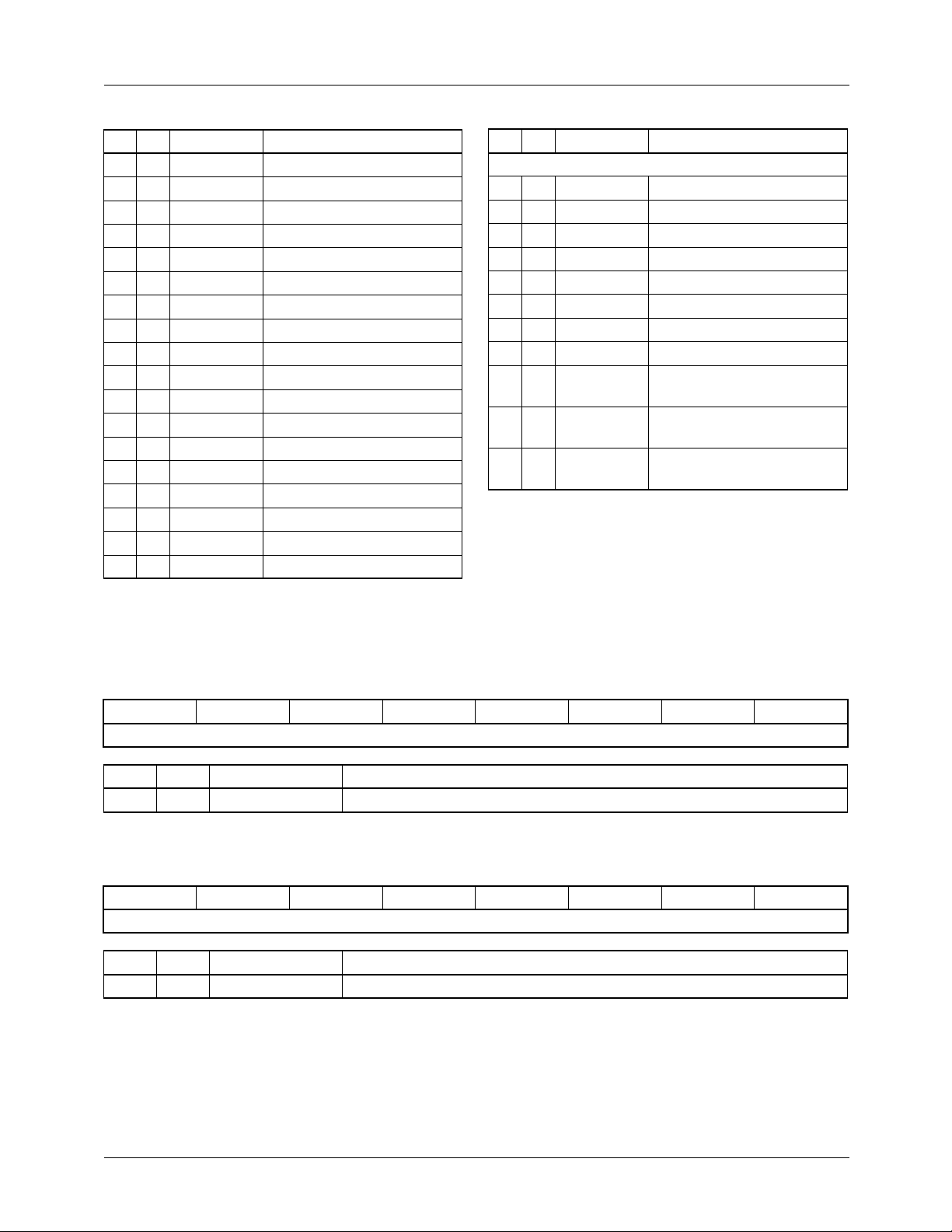
PRODUCT SPECIFICATION TMC2192
Table 22. Control Register Map (continued)
Reg Bit Mnemonic Function
38 7-0 Reserved Program Low
39 7-0 Reserved Program Low
3A 7-4 MCF1M Matrix Coefficient #1
3A 3-0 Reserved Program Low
3B 7-3 Reserved Set to 0.
3B 2-0 MCF4M Matrix Coefficient #4
3C 7-3 Reserved Set to 0.
3C 2-0 MCF6M Matrix Coefficient #6
3D 7-4 Reserved Program Low
3D 3-0 Reserved Program Low
3E 7-4 Reserved Program Low
3E 3-0 Reserved Program Low
3F 7 SEL_CLK DCVBS Clock Select
3F 6 Reserved Program Low
3F 5 GAUSS_BVP Gaussian Bypass Select
3F 4 SEL_PIX DCVBS Output Selection
3F 3 C2DB_OFF COMP2DB Offset Selection
3F 2-0 Reserved Program Low
Table 22. Control Register Map (continued)
Reg Bit Mnemonic Function
Subcarrier Registers
40 7-0 FREQL Subcarrier Frequency
41 7-0 FREQ3 Subcarrier Frequency
42 7-0 FREQ2 Subcarrier Frequency
43 7-0 FREQM Subcarrier Frequency
44 7-0 SYSPHL System Phase
45 7-0 SYSPHM System Phase
46 7-0 BURPHL Burst Phase
47 7-0 BURPHM Burst Phase
48 7-0 BRSTFULL Burst Height – Maximum
Amplitude
49 7-0 BRST1 Burst Height – 1st Intermediate
Value
4A 7-0 BRST2 Burst Height – 2nd Intermediate
Value
Note:
1. For each register listed above, all bits not specified are
reserved and should be set to logic LOW to ensure proper
operation.
Control Register Definitions
Part Identification Register (0x00)
76543210
PARTID2
Reg Bit Name Description
00 7-0 PARTID2 (Read Only) 0x97
Part Identification Register (0x01)
76543210
PARTID1
Reg Bit Name Description
01 7-0 PARTID1 (Read Only) 0x21
REV. 1.0.0 8/13/03 35
Page 36
TMC2192 PRODUCT SPECIFICATION
Control Register Definitions (continued)
Part Identification Register (0x02)
76543210
PARTID0
Reg Bit Name Description
02 7-0 PARTID0 (Read Only) 0x92
Revision Identification Register (0x03)
76543210
REVID0
Reg Bit Name Description
03 7-0 REVID0 Reads back the revision number of the part.
Gamma Filters Register (0x04)
76543210
RESERVED RESERVED RESERVED RESERVED SRESET
SKEN PDRM
Reg Bit Name Description
04 7-4 RESERVED Set to Low
04 3 SRESET Software RESET.
When LOW, resets internal state machines and disables outputs.
When HIGH, state machines are active and outputs are enabled.
04 2 SKEN Data KEY Enable.
When SKEN is LOW, Data keying is disabled.
When SKEN is HIGH, Data keying is enabled.
04 1-0 PDRM Pixel Data Ramping Mode. Pixel Data weighting for the rising edge of
active video.
NTSC: 0 0 1/8 1/2 7/8 1 1
PAL: 0 1/8 3/8 5/8 7/8 1 1
00 Pixels are weighted on the edge.
01 Sample and hold the 5th pixel for the slope weighting
1X Hard switch 000111
36 REV. 1.0.0 8/13/03
Page 37

PRODUCT SPECIFICATION TMC2192
Control Register Definitions (continued)
Input Format Register (0x05)
76543210
D10FF INMODE OMIX SOURCE
Reg Bit Name Description
05 7 D1OFF YCBCR Input Formatting.
When D1OFF is HIGH, 64 is subtracted from Y data path of the PD port.
When D1OFF is LOW, pixel data is passed through.
05 6 Reserved Program Low
05 5-4 INMODE Input Mode Select.
00 24 bit YC
01 10 bit D1 (YCBCR) PD[23:14] = YCBCR at 27MHz
10 20 bit YCBCR (4:4:4) PD[9:0] = Y PD[23:14] = CBCR (at 27MHz)
11 20 bit YCBCR (4:2:2) PD[9:0] = Y PD[23:14] = CBCR
05 3-2 OMIX Overlay Mixer Select.
00 No mix – PD data is always passed
01 Hard mix – mixer performs a hard switch between PD and Overlay
10 Set1 mix – the pixel data has the following weighting on the
transition; 0, 1/2, 1
11 Set2 mix – the pixel data has the following weighting on the
transition; 0, 1/8, 1/2, 7/8, 1
05 1-0 SOURCE Video Input Select. Chooses from internal test patterns or pixel data port.
00 PD PORT
01 Modulated Ramp
10 INTERNAL COLOR BAR (75%)
11 INTERNAL COLOR BAR (100%)
(4:4:4) PD[7:0] = Y PD[23:16] = CB PD[15:8] = C
BCR
R
REV. 1.0.0 8/13/03 37
Page 38
TMC2192 PRODUCT SPECIFICATION
Control Register Definitions (continued)
General Control Register (0x06)
76543210
FORMAT MODE PDCDIR TOUT TSOUT
Reg Bit Name Description
06 7-6 FORMAT Video Format.
00 NTSC
01 PAL – B,G,H,I,N
10 PAL – M
11 Reserved
06 5-3 MODE Video Mode.
000 MASTER with free-running subcarrier
001 SLAVE with free-running subcarrier
010 CCIR656 with free-running subcarrier
011 GENLOCK with subcarrier phase and frequency locked to the GRS
information.
100 MASTER with subcarrier phase reset every 8 fields
101 SLAVE with subcarrier phase reset every 8 fields
110 CCIR656 with subcarrier phase reset every 8 fields.
111 DRS-Lock with subcarrier phase and frequency locked to the DRS
information.
06 2 PDCDIR PDC Directional Control.
06 1 TOUT External Sync Output Control.
06 0 TSOUT External Sync Delay Control.
When PDC is LOW, the PDC pin is an output.
When PDCDIR is HIGH, the PDC pin is an input that can override the
internally generated PDC and blank the active video of a line.
When TOUT = LOW, a MPEG style field toggle is the output on pin VSOUT
When TOUT = HIGH, a traditional vertical sync is the output on pin VSOUT.
When the TSOUT is LOW, HSOUT, VSOUT are delayed to match
propagation delay through the chip. When TSOUT is HIGH, HSOUT,
VSOUT are aligned with the incoming data on the PD port.
.
38 REV. 1.0.0 8/13/03
Page 39
PRODUCT SPECIFICATION TMC2192
Control Register Definitions (continued)
Horizontal Ancillary Data Control Register (0x07)
76543210
LDFID SKFLIP DDSRST RESERVED ANCFREN ANCPHEN ANCTREN
Reg Bit Name Description
07 7 LDFID Field Lock Select. When LDFID is HIGH, the FLD[2:0] pins are used as
inputs to lock the field the that the TMC2192 is encoding. 5 PXCK’s after
the falling edge of HSIN the FLD[2:0] pins are sampled. When LDFID is
LOW, the FLD[2:0] pins output the current field that is being encoded.
07 6 SKFLIP Soft Key Inversion.
When SKFLP is LOW, the key generated by the data keying is a normal
state. When SKFLP is HIGH, the key generated by the data keying is a
inverted state.
07 5 DDSRST DDS Reset. By inserting a logic HIGH into this register the DDS
accumulator is reset to SYSPH value at the start of the next field 1 and
DDSRST is reset LOW. This enables the DDS to be reset when the
encoder is operating with a free running subcarrier.
07 4-3 RESERVED
07 2 ANCFREN Ancillary Frequency Enable.
When HIGH, the encoder gets subcarrier frequency data (FREQ3-0) from
incoming ancillary data (in accordance with FRV bit). When LOW,
FREQ3-0 registers contain the subcarrier frequency data.
07 1 ANCPHEN Ancillary Phase Enable.
When HIGH, the encoder gets subcarrier phase offset data (SCHPHL and
SCHPHM) from incoming ancillary data (in accordance with PHV bit).
When LOW, a default value of 0000h is used for subcarrier phase.
07 0 ANCTREN Ancillary Timing Enable.
When HIGH, the encoder decodes incoming ancillary data to determine
video timing (FIELD and SVF). When LOW, the ancillary timing reference
data is ignored.
Ancillary Data ID Register (0x08)
76543210
ANCID
Reg Bit Name Description
08 7-0 ANCID Ancillary Data Identification.
Bits 7-0 determine the ancillary data identification. Bit 0 is an odd parity bit.
The value in this register must match that of the incoming ancillary data.
REV. 1.0.0 8/13/03 39
Page 40
TMC2192 PRODUCT SPECIFICATION
Control Register Definitions (continued)
Keying/Overlay Engine Register (0x09)
76543210
HKEN BUKEN SKEXT DKDIS EKDIS FKDIS LAYMODE
Reg Bit Name Description
09 7 HKEN Hardware KEY Enable.
When LOW, the KEY pin is ignored.
When HIGH, the KEY pin is enabled.
09 6 BUKEN Burst KEY Enable.
When LOW, the output video burst is generated internally.
When HIGH, the output video burst is taken from the CVBS port.
09 5 SKEXT Data KEY Operation Select.
When LOW, data keying is allowed only during active video window.
When HIGH, data keying is allowed during frame.
09 4 DKDIS Y Data KEY Disable.
When LOW, Y input data is enabled for data keying.
When HIGH, Y input data is ignored for data keying.
09 3 EKDIS C
09 2 FKDIS CR Data KEY Disable.
09 1-0 LAYMODE Layer Assignment Select.
Data KEY Disable.
B
When LOW, CB input data is enabled for data keying.
When HIGH, CB input data is ignored for data keying.
When LOW, CR input data is enabled for data keying.
When HIGH, CR input data is ignored for data keying.
BACKGND
Mode
Source
0 PD OVERLAY 0L4-0 CVBS KEY
1 PD CVBS KEY OVERLAY OL4-0
2 CVBS OVERLAY OL4-0 PD KEY
3 CVBS PD KEY OVERLAY OL4-0
MIDGND
Source Key
FOREGND
Source Key
40 REV. 1.0.0 8/13/03
Page 41
PRODUCT SPECIFICATION TMC2192
Control Register Definitions (continued)
Key Value Register (0x0A)
76543210
DKEYMAX
Reg Bit Name Description
0A 7-0 DKEYMAX Y Maximum Data Key Value.
DKEYMAX is compared against the 8 MSB’s of Y channel. If DKEYMAX is
greater or equal to Y and DKEYMIN less than Y then a match is signaled.
Key Value Register (0x0B)
76543210
DKEYMIN
Reg Bit Name Description
0B 7-0 DKEYMIN Y Minimum Data Key Value.
DKEYMIN is compared against the 8 MSB’s of Y channel. If DKEYMAX is
greater or equal to Y and DKEYMIN less than Y then a match is signaled.
Key Value Register (0x0C)
76543210
EKEYMAX
Reg Bit Name Description
0C 7-0 EKEYMAX C
Maximum Data Key Value.
B
EKEYMAX is compared against the 8 MSB’s of CB channel. If EKEYMAX is
greater or equal to CB and EKEYMIN less than CB then a match is signaled.
Key Value Register (0x0D)
76543210
EKEYMIN
Reg Bit Name Description
0D 7-0 DKEYMIN CB Minimum Data Key Value.
EKEYMIN is compared against the 8 MSB’s of CB channel. If EKEYMAX is
greater or equal to CB and EKEYMIN less than CB then a match is signaled
REV. 1.0.0 8/13/03 41
Page 42
TMC2192 PRODUCT SPECIFICATION
Control Register Definitions (continued)
Key Value Register (0x0E)
76543210
FKEYMAX
Reg Bit Name Description
0E 7-0 FKEYMAX C
Maximum Data Key Value.
R
FKEYMAX is compared against the 8 MSB’s of C
greater or equal to C
and FKEYMIN less than CR then a match is signaled.
R
channel. If FKEYMAX is
R
Key Value Register (0x0F)
76543210
FKEYMIN
Reg Bit Name Description
0F 7-0 FKEYMIN C
Minimum Data Key Value.
R
FKEYMIN is compared against the 8 MSB’s of CR channel. If FKEYMAX is
greater or equal to CR and FKEYMIN less than CR then a match is signaled.
42 REV. 1.0.0 8/13/03
Page 43

PRODUCT SPECIFICATION TMC2192
Control Register Definitions (continued)
DAC Control Register (0x10)
76543210
COMPDIS CHROMADIS LUMADIS RESERVED RESERVED OLUTDIS RESERVED
Reg Bit Name Description
10 7 COMPDIS Composite D/A Disable.
When COMPDIS is LOW, the COMPOSITE D/A is enabled.
When COMPDIS is HIGH, the COMPOSITE D/A is disabled.
10 6 CHROMADIS Chroma D/A Disable.
When CHROMADIS is LOW, the CHROMA D/A is enabled.
When CHROMADIS is HIGH, the CHROMA D/A is disabled.
10 5 LUMADIS LUMA D/A Disable.
When LUMADIS is LOW, the LUMA D/A is enabled.
When LUMADIS is HIGH, the LUMA D/A is disabled.
10 4-3 RESERVED Set to 0.
10 2 OLUTDIS Overlay LUT Disable.
When OLUTDIS is LOW, the olut is enabled.
When OLUTDIS is HIGH, the olut is disabled.
10 1-0 RESERVED Program Low
REV. 1.0.0 8/13/03 43
Page 44

TMC2192 PRODUCT SPECIFICATION
Control Register Definitions (continued)
DAC Control Register (0x11)
76543210
DRSSEL RESERVED COMP2DB SINEN REFSEL LUMDIS CHRMDIS BURSTDIS
Reg Bit Name Description
11 7 DRSSEL DRS Selection.
When DRSSEL is HIGH, PD[7:0] is routed to the DRS detection block.
When DRSSEL is LOW, CVBS[9:2] is routed to the DRS detection block.
11 6 RESERVED Program Low
11 5 COMP2DB. Composite 2 Overflow Control.
When COMP2DB is HIGH, the digital range of the composite sumer is 0 to
2047 with half the digital resolution. When COMP2DB is LOW, the digital
output of the composite summer is 0 to 1023, all values exceeding 1023 or
below 0 are clipped.
11 4 SINEN X/Sine(X) Filter Enable.
When SINEN is LOW, the X/Sin(X) filter is bypassed.
When SINEN is HIGH, the X/Sin(X) filter is used to compensate for the
DAC roll-off at high frequencies.
11 3 RESERVED Program Low
11 2 LUMDIS Luma Disable.
When LUMDIS is LOW, the luminance data on the composite data path is
11 1 CHRMDIS Chroma Disable.
11 0 BURSTDIS Burst Disable.
enabled. When LUMDIS is HIGH, the luminance data on the composite
data path is disabled.
When CHRMDIS is LOW, the chrominance data on the composite data
path is enabled. When CHRMDIS is HIGH, the chrominance data on the
composite data path is disabled.
When BURSTDIS is LOW, the burst is enabled.
When BURSTDIS is HIGH, the burst is disabled.
44 REV. 1.0.0 8/13/03
Page 45
PRODUCT SPECIFICATION TMC2192
Control Register Definitions (continued)
VBI Ped Enable Register (0x14)
76543210
VBIPEDEM
Reg Bit Name Description
14 7-0 VBIPEDEM VBI Pedestal Enable, Even Fields.
VBIPEDEM is the bits 15-8 of VBIPEDE[15:0]. VBIPEDE controls the
addition of pedestal on a line by line basis from line 10 in NTSC
(VBIPEDE[0] = HIGH) to line 24 (VBIPEDE[14] = HIGH) in the EVEN field
of NTSC. VBIPEDE[15] controls the pedestal from line 25 to line 263
inclusive.
VBI Ped Enable Register (0x15)
76543210
VBIPEDEL
Reg Bit Name Description
15 7-0 VBIPEDEL VBI Pedestal Enable, Even Fields.
VBIPEDEL is the bits 7-0 of VBIPEDE[15:0]. VBIPEDE controls the
addition of pedestal on a line by line basis from line 10 in NTSC
(VBIPEDE[0] = HIGH) to line 24 (VBIPEDE[14] = HIGH) in the EVEN field
of NTSC. VBIPEDE[15] controls the pedestal from line 25 to line 263
inclusive.
VBI Ped Enable Register (0x16)
76543210
VBIPEDOM
Reg Bit Name Description
16 7-0 VBIPEDOM VBI Pedestal Enable, Odd Fields.
VBIPEDOM is the bits 14-7 of VBIPEDO[14:0]. VBIPEDO controls the
addition of pedestal on a line by line basis from line 273 (VBIPEDE[0] =
HIGH) to line 286 (VBIPEDE[13] = HIGH) in the ODD field of NTSC.
VBIPEDO[14] controls the pedestal from line 287 to line 525 inclusive.
REV. 1.0.0 8/13/03 45
Page 46
TMC2192 PRODUCT SPECIFICATION
Control Register Definitions (continued)
VBI Ped Enable Register (0x17)
76543210
VBIPEDOL HVA
Reg Bit Name Description
17 7-1 VBIPEDOM VBI Pedestal Enable, Odd Fields.
VBIPEDOL is the bits 6-0 of VBIPEDO[14:0]. VBIPEDO controls the
addition of pedestal on a line by line basis from line 273 (VBIPEDE[0] =
HIGH) to line 286 (VBIPEDE[13] = HIGH) in the ODD field of NTSC.
VBIPEDO[14] controls the pedestal from line 287 to line 525 inclusive.
17 0 HVA Horizontal and Vertical Sync Alignment.
When HVA is LOW, the falling edge of HSIN
to the rising edge of PXCK to start an field 1. When HVA is HIGH, VSIN is
allowed to vary from HSIN by ±32 pixels.
and VSIN must occur just prior
Vertical Blanking Interval Enable Register (0x18)
76543210
Reserved GLKCTL1 GLKCTL0 VBIENF1
Reg Bit Name Description
18 7 Reserved
18 6 GLKCTL1 Genlock Control Register 1.
When GLKCTL1 is LOW, the PALODD bit of the GRS stream is ignored.
When GLKCTL1 is HIGH, the PALODD bit of the GRS stream controls the
PALODD flip of the subcarrier.
18 5 GLKCTL0 Genlock Control Register 0.
When GLKCTL0 is LOW, the Color Frame bit of the GRS stream is ignored.
When GLKCTL0 is HIGH, the Color Frame bit of the GRS stream controls
the field sequence in the FVHGEN.
18 4-0 VBIENF VBI Active Video Enable, Field 1.
The value of VBIENF1 determines which line blanking stops and active line
for EVEN fields in NTSC starting from line 4 to line 35 or an ODD fields for
PAL starting from line 1 to line 32.
46 REV. 1.0.0 8/13/03
Page 47
PRODUCT SPECIFICATION TMC2192
Control Register Definitions (continued)
Vertical Blanking Interval Enable Register (0x19)
76543210
SHORT T512 HALFEN
Reg Bit Name Description
19 7 SHORT Test Register. Program LOW.
19 6 T512 EH/SL Offset Control Bit.
When LOW, the true value of EH and SL is offset by 256.
When HIGH, the true value of EH and SL is offset by 512.
19 5 HALFEN
19 4-0 VBIENF2 VBI Active Video Enable, Field 2.
Half Line Enable.
When LOW, half-line blanking occurs on line 283 (NTSC) or line 23 (PAL).
When HIGH, line 283 (NTSC) or line 23 (PAL) is treated as a full line of
active video.
The value of VBIENF2 determines which line blanking stops and active line
for ODD fields in NTSC starting from line 4 to line 35 or an EVEN fields for
PAL starting from line 1 to line 32.
VBIENF2
Pedestal Height Register (0x1A)
Reg Bit Name Description
1A 7 Reserved
1A 6-0 PEDHGT1 Composite Pedestal Height.
76543210
Reserved PEDHGT1
PEDHGT1 is a 2’s comp value producing a pedestal height from -22.1 IRE
to 21.7 IRE with .345 IRE steps on the composite data path. The default 7.5
IRE pedestal for NTSC-M results from a hex code of 0010110b.
Closed Caption Register (0x1C)
76543210
CCD1
Reg Bit Name Description
1C 7-0 CCD1 First Byte of CC Data.
Bit 0 is the LSB. The MSB will be overwritten by an ODD Parity Bit if
CCPAR is HIGH.
REV. 1.0.0 8/13/03 47
Page 48
TMC2192 PRODUCT SPECIFICATION
Control Register Definitions (continued)
Closed Caption Register (0x1D)
76543210
CCD2
Reg Bit Name Description
1D 7-0 CCD2 Second Byte of CC Data.
Bit 0 is the LSB. The MSB will be overwritten by an ODD Parity Bit if
CCPAR is HIGH
Closed Caption Register (0x1E)
76543210
CCON CCRTS CCPAR CCFLD CCLINE
Reg Bit Name Description
1E 7 CCON Enable CC Data Packet.
Command the CC data generator to send either CC data or a NULL byte
whenever the specified line is transmitted.
1E 6 CCRTS Request To Send Data.
This bit is set HIGH by the user when bytes 0x1C and 0x1D have been
1E 5 CCPAR Auto Parity Generation.
1E 4 CCFLD CC Field Select.
1E 3-0 CCLINE CC Line Select.
loaded with the next two bytes to be sent. When the encoder’s line count
reaches preceding the line specified in bits 4-0 of this register the data will
be transferred from registers 0x1C and 0x1D, and RTS will be RESET
LOW. A new pair of bytes may then be loaded into registers 0x1C and
0x1D. If CCON = 1 and CCRTS = 0 when the CC line is to be sent, NULL
bytes will be sent.
When set HIGH, the encoder replaces the MSB of bytes 0x1C and 0x1D
with a calculated ODD parity. When set LOW, the CC processor transmits
the 16 bits exactly as loaded into registers 0x1C and 0x1D.
When LOW, CC data is transmitted on the selected line of ODD fields.
When HIGH, it is sent on EVEN fields.
Defines (with an offset) the line on which CC data are transmitted.
Timing Register (0x1F)
76543210
PDCNT
Reg Bit Name Description
1F 7-0 PDCNT Pixel Data Control Start.
PDCNT determines the number of pixels (PCK’s) from the midpoint of the
falling edge of horizontal sync to the rising edge of PDC on active video
lines.
48 REV. 1.0.0 8/13/03
Page 49
PRODUCT SPECIFICATION TMC2192
Control Register Definitions (continued)
Timing Register (0x20)
76543210
SY
Reg Bit Name Description
20 7-0 SY Horizontal Sync Tip Duration.
This 8 bit register holds a value extending from 0 to 255 PCK cycles.
Timing Register (0x21)
76543210
BR
Reg Bit Name Description
21 7-0 BR Breezeway Duration.
This 8 bit register holds a value extending from 0 to 255 PCK cycles.
Timing Register (0x22)
76543210
BU
Reg Bit Name Description
22 7-0 BU Burst Duration.
This 8 bit register holds a value extending from 0 to 255 PCK cycles.
Timing Register (0x23)
76543210
CBP
Reg Bit Name Description
23 7-0 CBP Color Back Porch Duration.
This 8 bit register holds a value extending from 0 to 255 PCK cycles.
Timing Register (0x24)
76543210
XBP
Reg Bit Name Description
24 7-0 CBP Extended Color Back Porch Duration.
This 8 bit register holds the LSB’s of a 10 bit value extending from 0 to 1023
PCK cycles.
REV. 1.0.0 8/13/03 49
Page 50
TMC2192 PRODUCT SPECIFICATION
Control Register Definitions (continued)
Timing Register (0x25)
76543210
VA
Reg Bit Name Description
25 7-0 VA Active Video Region Duration.
This 8 bit register holds the LSB’s of a 10 bit value extending from 0 to 1023
PCK cycles.
Timing Register (0x26)
76543210
VC
Reg Bit Name Description
26 7-0 VC Active Video Region 2
This 8 bit register holds the LSB’s of a 10 bit value extending from 0 to 1023
PCK cycles.
nd
Half Line Duration.
Timing Register (0x27)
76543210
VB
Reg Bit Name Description
27 7-0 VB Active Video Region 1st Half Line Duration.
This 8 bit register holds the LSB’s of a 10 bit value extending from 0 to 1023
PCK cycles.
Timing Register (0x28)
76543210
VB
Reg Bit Name Description
28 7-0 EL Equalization Pulse Low Duration.
This 8 bit register holds a value extending from 0 to 255 PCK cycles.
50 REV. 1.0.0 8/13/03
Page 51
PRODUCT SPECIFICATION TMC2192
Control Register Definitions (continued)
Timing Register (0x29)
76543210
EH
Reg Bit Name Description
29 7-0 EH Equalization Pulse High Duration.
This 8 bit register holds 8 LSB’s of EH, The addition of 256 or 512 is
controlled by T512. The range is either 256 to 511 PCK cycles or 512 to
767 PCK cycles.
Timing Register (0x2A)
76543210
SL
Reg Bit Name Description
2A 7-0 SL Vertical Sync Pulse Low Duration.
This 8 bit register holds 8 LSB’s of SL, The addition of 256 or 512 is
controlled by T512. The range is either 256 to 511 PCK cycles or 512 to
767 PCK cycles.
Timing Register (0x2B)
76543210
SH
Reg Bit Name Description
2B 7-0 SH Vertical Sync Pulse High Duration.
This 8 bit register holds a value extending from 0 to 255 PCK cycles.
Timing Register (0x2C)
76543210
FP
Reg Bit Name Description
2C 7-0 FP Front Porch Duration.
This 8 bit register holds a value extending from 0 to 255 PCK cycles.
REV. 1.0.0 8/13/03 51
Page 52
TMC2192 PRODUCT SPECIFICATION
Control Register Definitions (continued)
Timing Register (0x2D)
76543210
XBP VA VB VC
Reg Bit Name Description
2D 7-6 XBP Extended Color Back Porch Duration.
2 MSB’s of the 10 bit XBP, extending from 0 to 1023 PCK cycles.
2D 5-4 VA Active Video Duration.
2 MSB’s of the 10 bit VA, extending from 0 to 1023 PCK cycles.
2D 3-2 VB Active Video Region 1st Half Line Duration.
2 MSB’s of a 10 bit VB, extending from 0 to 1023 PCK cycles.
2D 1-0 VC Active Video Region 2
2 MSB’s of a 10 bit VC, extending from 0 to 1023 PCK cycles.
nd
Half Line Duration.
Timing Register (0x2E)
76543210
FIELD LTYPE
Reg Bit Name Description
2E 7-5 FIELD Field Identification. (READ ONLY)
These three bits are updated 12 PXCK periods after each vertical sync.
They allow the user to determine field type on a continuous basis
2E 4-0 LTYPE LineType Identification (READ ONLY)
These three bits are updated 5 PXCK periods after each horizontal sync.
They allow the user to determine line type on a continuous basis.
Timing Register (0x2F)
76543210
CBL
Reg Bit Name Description
2F 7-0 CBL Color Bar Duration.
This 8 bit register holds a value extending from 0 to 255 PCK cycles.
Color Space Matrix Register (0x30)
76543210
MCF1L
Reg Bit Name Description
30 7-0 MCF1L Matrix Coefficient #1.
Bits 7-0 of MCF1.
52 REV. 1.0.0 8/13/03
Page 53
PRODUCT SPECIFICATION TMC2192
Control Register Definitions (continued)
Color Space Matrix Register (0x31)
76543210
RESERVED
Reg Bit Name Description
31 7-0 RESERVED Program Low
Color Space Matrix Register (0x32)
76543210
RESERVED
Reg Bit Name Description
32 7-0 RESERVED Program Low
Color Space Matrix Register (0x33)
76543210
MCF2L
Reg Bit Name Description
33 7-0 MCF2L Matrix Coefficient #2.
Bits 7-0 of MCF4.
Color Space Matrix Register (0x34)
76543210
RESERVED
Reg Bit Name Description
34 7-0 RESERVED Program Low
Color Space Matrix Register (0x35)
76543210
MCF3L
Reg Bit Name Description
35 7-0 MCF3L Matrix Coefficient #3.
Bits 7-0 of MCF6.
REV. 1.0.0 8/13/03 53
Page 54
TMC2192 PRODUCT SPECIFICATION
Control Register Definitions (continued)
Color Space Matrix Register (0x36)
76543210
RESERVED
Reg Bit Name Description
36 7-0 RESERVED Program Low
Color Space Matrix Register (0x37)
76543210
RESERVED
Reg Bit Name Description
37 7-0 RESERVED Program Low
Color Space Matrix Register (0x38)
76543210
Reg Bit Name Description
38 7-0 RESERVED Program Low
Color Space Matrix Register (0x39)
76543210
Reg Bit Name Description
39 7-0 RESERVED Program Low
Color Space Matrix Register (0x3A)
76543210
MCF1M MCF2M
Reg Bit Name Description
3A 7-4 MCF1M Matrix Coefficient #1.
Bits 11-8 of MCF1.
3A 3-0 RESERVED Program Low
RESERVED
RESERVED
54 REV. 1.0.0 8/13/03
Page 55
PRODUCT SPECIFICATION TMC2192
Control Register Definitions (continued)
Color Space Matrix Register (0x3B)
76543210
MCF3M RESERVED MCF4M
Reg Bit Name Description
3B 7-3 RESERVED Set to 0.
3B 2-0 MCF4M Matrix Coefficient #4.
Bits 10-8 of MCF4.
Color Space Matrix Register (0x3C)
76543210
MCF5M RESERVED MCF6M
Reg Bit Name Description
3C 7-3 RESERVED Set to 0.
3C 2-0 MCF6M Matrix Coefficient #6.
Bits 10-8 of MCF6.
Color Space Matrix Register (0x3D)
76543210
RESERVED RESERVED
Reg Bit Name Description
3D 7-4 RESERVED Program Low
3D 3-0 RESERVED Program Low
Color Space Matrix Register (0x3E)
76543210
RESERVED RESERVED
Reg Bit Name Description
3E 7-4 RESERVED Program Low
3E 3-0 RESERVED Program Low
REV. 1.0.0 8/13/03 55
Page 56
TMC2192 PRODUCT SPECIFICATION
Control Register Definitions (continued)
Color Space Matrix Register (0x3F)
76543210
SEL_CLK RESERVED GAUSS_BYP SEL_PIX C2DB_OFF NMEH CSMFMT
Reg Bit Name Description
3F 7 SEL_PIX DCVBS Output Selection.
When SEL_PIX is HIGH, the interpolated pixel data is selected as the
output for the DCVBS port. When SEL_PIX is LOW, the non-interpolated
pixel data is selected as the output for the DCVBS port.
3F 6 RESERVED Program Low
3F 5 GAUSS_BYP Gaussian Bypass Select.
When GAUSS_BYP is LOW, the gaussian filter is enabled.
When GAUSS_BYP is HIGH, the gaussian filter is bypassed.
3F 4 SEL_CLK DCVBS Clock Select.
When SEL_CLK is LOW, the DCVBS output is clocked at the PXCK.
When SEL_CLK is HIGH, the DCVBS output is clocked at the PCK.
3F 3 C2DB_OFF COMP2DB Offset Selection.
When C2DB_OFF is HIGH an offset of 256 is added to the COMP2 output
allowing the chrominance data that extends below the sync level to be
passed through the outputs.
3F 2-0 RESERVED Program Low
Subcarrier Register (0x40)
76543210
Reg Bit Name Description
40 7-0 FREQL Subcarrier Frequency.
Bits 7-0 of the subcarrier frequency FREQL[31:0].
FREQL
56 REV. 1.0.0 8/13/03
Page 57
PRODUCT SPECIFICATION TMC2192
Control Register Definitions (continued)
Subcarrier Register (0x41)
76543210
FREQ3
Reg Bit Name Description
41 7-0 FREQ3 Subcarrier Frequency.
Bits 15-8 of the subcarrier frequency FREQL[31:0].
Subcarrier Register (0x42)
76543210
FREQ2
Reg Bit Name Description
42 7-0 FREQ2 Subcarrier Frequency.
Bits 23-16 of the subcarrier frequency FREQL[31:0].
Subcarrier Register (0x43)
76543210
FREQM
Reg Bit Name Description
43 7-0 FREQM Subcarrier Frequency.
Bits 31-24 of the subcarrier frequency FREQL[31:0].
Subcarrier Register (0x44)
76543210
SYSPHL
Reg Bit Name Description
44 7-0 SYSPHL System Phase.
Bits 7-0 of the video phase offset SYSPH[15:0].
Subcarrier Register (0x45)
76543210
SYSPHM
Reg Bit Name Description
45 7-0 SYSPHM System Phase.
Bits 15-8 of the video phase offset SYSPH[15:0].
REV. 1.0.0 8/13/03 57
Page 58
TMC2192 PRODUCT SPECIFICATION
Control Register Definitions (continued)
Subcarrier Register (0x46)
76543210
BURPHL
Reg Bit Name Description
46 7-0 BURPHL Burst Phase.
Bits 7-0 of the burst phase offset BURPH[15:0].
Subcarrier Register (0x47)
76543210
BURPHM
Reg Bit Name Description
47 7-0 BURPHM Burst Phase.
Bits 15-8 of the burst phase offset BURPH[15:0].
Burst Height Register (0x48)
76543210
BRSTFULL
Reg Bit Name Description
48 7-0 BRSTFULL Burst Height – Maximum Amplitude.
The 8 bit value assigned to U burst component in NTSC and to the U and V
components in PAL for the maximum burst amplitude. The burst envelopes
midpoint is derived from BRSTFULL. The value programmed into
BRSTFULL needs to be .707 of the magnitude of the burst vector.
Burst Height Register (0x49)
76543210
BRST1
Reg Bit Name Description
49 7-0 BRST1 Burst Height – 1st Intermediate Value.
The 8 bit value assigned to U burst component in NTSC and to the U and V
components in PAL for the first intermediate value of the burst envelope.
The value programmed into BRST1 needs to be .707 of the magnitude of
the burst vector.
58 REV. 1.0.0 8/13/03
Page 59
PRODUCT SPECIFICATION TMC2192
Control Register Definitions (continued)
Subcarrier Register (0x4A)
76543210
BRST2
Reg Bit Name Description
4A 7-0 BRST2 Burst Height – 2nd Intermediate Value.
The 8 bit value assigned to U burst component in NTSC and to the U and V
components in PAL for the second intermediate value of the burst
envelope. The value programmed into BRST2 needs to be .707 of the
magnitude of the burst vector.
REV. 1.0.0 8/13/03 59
Page 60
TMC2192 PRODUCT SPECIFICATION
Absolute Maximum Ratings (beyond which the device may be damaged)
Parameter Min. Max. Unit
Power Supply Voltage -0.5 7.0 V
Digital Inputs
Applied Voltage
Forced Current
Digital Outputs
Applied Voltage
Forced Current
Short Circuit Duration (Single Output in HIGH state to GND) 1 second
Analog Output Short Circuit Duration (Single output to GND) Infinite
Temperature
Operating, Ambient -20 +110 °C
Operating, Junction, Plastic package +150 °C
Lead, Soldering (10 seconds) +300 °C
Vapor Phase Soldering (1 minute) +220 °C
Storage -65 +150 °C
Notes:
1. Absolute maximum ratings are limiting values applied individually while all other parameters are within specified operating
conditions. Functional operation under any of these conditions is NOT implied.
2. Applied voltage must be current limited to specified range, and measured with respect to GND.
3. Forcing voltage must be limited to specified range.
4. Current is specified as conventional current, flowing into the device.
2
3,4
2
3,4
-0.5 VDD + 0.5 V
-20.0 20.0 mA
-0.5 VDD + 0.5 V
-20.0 20.0 mA
Operating Conditions
Parameter Min. Nom. Max. Units
V
DD
V
IH
V
IL
I
OH
I
OL
V
REF
I
REF
R
REF
R
OUT
T
A
Pixel Interface
f
PXL
f
PXCK
t
PWHPX
t
PWLPX
Power Supply Voltage 4.75 5.0 5.25 V
Input Voltage, Logic HIGH TTL Compatible Inputs 2.0 V
CMOS Compatible Inputs 0.7V
DD
DD
V
DD
Input Voltage, Logic LOW TTL Compatible Inputs GND 0.8 V
CMOS Compatible Inputs GND 0.3V
DD
Output Current, Logic HIGH -2.0 mA
Output Current, Logic LOW 4.0 mA
External Reference Voltage 1.235 V
D/A Converter Reference Current (I
flowing out of the R
Reference Resistor, V
pin)
REF
= Nom. 1210 Ω
REF
REF
= V
REF
/ R
REF
,
1.020 mA
Total Output Load Resistance 37.5 Ω
Ambient Temperature, Still Air 0 70 °C
Pixel Rate 10 15 Mpps
Master Clock Rate, 2x pixel rate 20 30 MHz
PXCK Pulse Width, HIGH 15 ns
PXCK Pulse Width, LOW 17.5 ns
V
V
V
60 REV. 1.0.0 8/13/03
Page 61
PRODUCT SPECIFICATION TMC2192
Operating Conditions (continued)
Parameter Min. Nom. Max. Units
t
SP
t
HP
Parallel Microprocessor Interface
t
PWLCS
t
PWHCS
t
SA
t
HA
t
SD
t
HD
t
SR
t
HR
Serial Interface
t
DAL
t
DAH
t
STAH
t
STASU
t
STOSU
t
BUFF
t
DSU
t
DHO
Setup Time 16 ns
Hold Time 0 ns
CS Pulse Width, LOW 4 PXCK
CS Pulse Width, HIGH 6 PXCK
Address Setup Time 17 ns
Address Hold Time 0 ns
Data Setup Time (write) 16 ns
Data Hold Time (write) 0 ns
RESET Setup Time 12 ns
RESET Hold Time 2 ns
SCL Pulse Width, LOW 1.3 µs
SCL Pulse Width, HIGH 0.6 µs
SDA Start Hold Time 0.6 µs
SCL to SDA Setup Time (Stop) 0.6 µs
SCL to SDA Setup Time (Start) 0.6 µs
SDA Stop Hold Time Setup 1.3 µs
SDA to SCL Data Setup Time 300 ns
SDA to SCL Data Hold Time 300 ns
REV. 1.0.0 8/13/03 61
Page 62
TMC2192 PRODUCT SPECIFICATION
Electrical Characteristics
Symbol Parameter Conditions Min. Typ. Max. Units
I
DD
I
DDQ
V
RO
I
BR
I
IH
I
IL
V
OH
V
OL
I
OZH
I
OZL
C
I
C
O
V
OC
R
OUT
C
OUT
Notes:
1. Typical I
2. Timing reference points are at the 50% level.
Power Supply Current VDD = Max., f
Power Supply Current
VDD = Max., f
= 27MHz 335 375 mA
PXCK
= 27MHz 15 25 mA
PXCK
(D/A disabled)
Voltage Reference Output 1.235 V
Input Bias Current, V
REF
Input Current, Logic HIGH V
Input Current, Logic LOW V
V
= Nom. 50 µA
REF
= Max., VIN = V
DD
= Max., VIN = GND -10 µA
DD
DD
10 µA
Output Voltage, Logic HIGH IOH = Max. 2.4 V
Output Voltage, Logic LOW IOL = Max. 0.4 V
Hi-Z Leakage current, HIGH VDD = Max., VIN = V
DD
10 µA
Hi-Z Leakage current, LOW VDD = Max., VIN = GND -10 µA
Digital Input Capacitance TA = 25°C, f = 1MHz 4 10 pF
Digital Output Capacitance TA = 25°C, f = 1MHz 10 pF
Video Output Compliance
-0.3 2.0 V
Voltage
Video Output Resistance 15 kΩ
Video Output Capacitance I
with VDD = +5.0 Volts and TA = 25°C.
DD
= 0 mA, f = 1 MHz 15 25 pF
OUT
Switching Characteristics
Parameter Conditions Min. Typ. Max. Units
PIPES Pipeline Delay PD to Analog Out
PD to DCVBS
t
DOZ
t
DOM
t
HOM
t
DO
Output Delay, CS to low-Z 4 15 ns
Output Delay, CS to Data Valid 15 ns
Output Hold Time, CS to hi-Z 10 ns
Output Delay PXCK to HSOUT, VSOUT,
PDC, LINE, FLD
t
R
t
F
t
DOV
Notes:
1. Timing reference points are at the 50% level.
2. Analog C
3. Pipeline delay, with respect to PXCK, is a function of the phase relationship between the internally generated PCK (PXCK/2)
and PXCK, as established by the hardware RESET
D/A Output Current Risetime 10% to 90% of full-scale 2 ns
D/A Output Current Falltime 90% to 10% of full-scale 2 ns
Analog Output Delay 10 ns
LOAD
<10 pF, D
load <40 pF.
7-0
.
64
66
PXCK
Periods
15 ns
62 REV. 1.0.0 8/13/03
Page 63
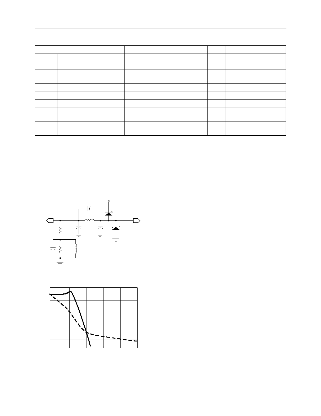
PRODUCT SPECIFICATION TMC2192
System Performance Characteristics
Parameter Conditions Min. Typ. Max. Units
RES D/A Converter Resolution 10 10 10 Bits
E
LI
E
LD
E
G
dp Differential Phase PXCK = 27.00 MHz,40 IRE Ramp 0.5 degree
dg Differential Gain PXCK = 27.00 MHz,40 IRE Ramp 0.9 %
SKEW CHROMA to LUMA Output
PSRR Power Supply Rejection
Notes:
1. TTL input levels are 0.0 and 3.0 Volts, 10%-90% rise and fall times <3 ns.
2. Analog CLOAD <10 pF, D7-0 load <40 pF.
Integral Linearity Error 0.25 %
Differential Linearity Error
0.10 %
(monotonic)
Gain Error ±7.5 %FS
01 ns
Skew
f=1kHz 0.5 %/%V
Ratio
DD
Applications Discussion
The suggested output reconstruction filter is shown in Figure
29. The phase and frequency response for the encoder and
the reconstruction filter is shown in Figure 30.
C6
27pF
A_IN A_OUT
R8
330pF
75Ω
C8
100pF
Figure 28. Typical Analog Reconstruction Filter
0
-10
R9
75Ω
C7
L5 1.8µH
L6
1.0µH
C7
330pF
D1
DIODE
SCHOTTKY
D2
DIODE
SCHOTTKY
65-6294-31
0
90
Phase (deg)
The circuit in Figure 31 shows the connection of power supply voltages, output reconstruction filters and the external
voltage reference. All VDD pins should be connected to the
same power source.
The full-scale output voltage level for each D/A:
V
OUTx
= I
OUTx
= K x (V
x RLx = K x I
REF/RREFx
) x R
REFx
Lx
x R
Lx
where:
•I
is the full-scale output current sourced by the D/A
OUTx
converter.
•RLx is the resistive load on the D/A output pin.
• K is a constant for the TMC2192 D/A converters (approximately equal to 34).
•I
is the reference current flowing out of the R
REFx
REFx
pin to ground.
•V
•R
is the voltage measured on the V
REF
is the total resistance connected between the
REFx
R
pin and ground.
REFx
REF
pin.
-20
-30
Attenuation (dB)
-40
0 5 10 15 20 25
Frequency (MHz)
180
270
360
65-6294-32
The reference voltage in Figure 31 is from an LM185 1.2
Volt band-gap reference. The suggested trim is designed to
give ±10% of trim around 5K Ohms. This R
"gain" for that D/A converter. Varying R
REFx
sets the
REFx
±10% will
cause the full-scale output voltage on the D/A to vary by
±10%.
An alternative output reconstruction filter is the Microelectronic Modules Corp. ST-163E, which contains 4 indepen-
Figure 29. Overall Response
dent reconstruction filter. The phase and frequency response
of this filter is shown in the Output Low-Pass Filters Section
of this data sheet.
REV. 1.0.0 8/13/03 63
Page 64

TMC2192 PRODUCT SPECIFICATION
Layout Considerations
Designing with high-performance mixed-signal circuits
demands printed circuits with ground planes. Wire-wrap is
not an option. Overall system performance is strongly influenced by the board layout. Capacitive coupling from digital
to analog circuits may result in poor picture quality. Consider the following suggestions when doing the layout:
• Keep analog traces (C
short and far from all digital signals as possible. The
TMC2192 should be located near the board edge, close
to the analog output connectors.
• The power plane for the TMC2192 should be separate
from that which supplies other digital circuitry. A single
power plane should be used for all of the V
the power supply for the TMC2192 is the same for the
system's digital circuitry, power to the TMC2192 should
be filtered with ferrite beads and 0.1µF capacitors to
reduce noise.
• The ground plane should be solid, not cross-hatched.
Connections to the ground plane should be very short.
BYPx
, V
REF
, R
, DACx) as
REF
DD
pins. If
• Decoupling capacitors should be applied liberally to
pins. For best results, use 0.1µF capacitors. Lead lengths
should be minimized. Ceramic chip capacitors are the
best choice.
• If there is dedicated digital power plane, it should not
overlap the TMC2192 footprint, the voltage reference,
or the analog outputs. Capacitive coupling of digital
power supply noise from this layer to the TMC2192 and
its related analog circuitry can have an adverse effect on
performance.
• The PXCK should be handled carefully. Jitter and noise
on this clock or its ground reference will translate to
noise on the video outputs. Terminate the clock line
carefully to eliminate overshoot and ringing.
• Connect all unused inputs to the TMC2192 to either
ground or VDD. Do not leave them unconnected.
64 REV. 1.0.0 8/13/03
Page 65
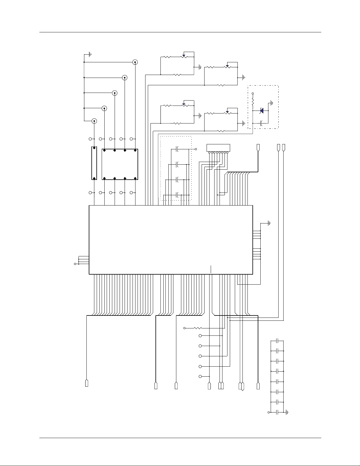
PRODUCT SPECIFICATION TMC2192
2
R31
10K Ohm
R39
10K Pot
13
R35
8.25K Ohm
2
R29
10K Ohm
R37
10K Pot
13
R33
8.25K Ohm
C58
0.1uF
C57
0.1uF
C56
0.1uF
AND CBYPy PIN DIRECTLY
CONNECT Cx TO VDDA PIN
C55
0.1uF
VDD
R30
10K Ohm
R28
10K Ohm
1234567
JP13
2
R38
10K Pot
13
R34
8.25K Ohm
2
R36
10K Pot
13
R32
8.25K Ohm
8
DCVBS1
DCVBS2
DCVBS0
DCVBS3
DCVBS4
DCVBS6
DCVBS5
DCVBS7
DCVBS8
R27
DCVBS9
VDD
3.3K Ohm
1
DCVBS[0..9]
D4
1.235V
C54
0.1uF
DCVBS[0..9]
2
STUFF EITHER C54 OR D4
HSOUT
VSOUT
J2
2
1
TP17
ORDA
{Schematic}
A_IN A_OUT
LPF
TP16
RDA
RDAC
2
TP19
ODA1
ST-163E
TP18
DA1
1
J3
AOUT
AIN
DAC1
2
TP21
TP20
1
ODA2
DA2
J4
DOUT
DIN
DAC2
2
TP23
TP22
J5
1
ODA3
DA3
DAC3
BOUT
BIN
2
TP25
TP24
J6
ODA4
DA4
DAC4
1
COUTCIN
{Schematic}
VCC
U?
96
72
54
39
PD[0..23]
PD[0..23]
19
PD0
AGND
51
PD1
1
7
12
13
18
AGND
R_LUMA
R_CHROMA
PD2327PD2228PD2129PD2030PD1931PD1832PD1733PD1634PD1535PD1436PD1337PD12
PD22
PD23
OLENG[0..5]
OLENGI[0..5]
98
V_REF
25
OLENG0
6
3
C_COMP
OLENG2
OLENG1
16
11
C_LUMA
C_CHROMA
OLENG3
OLENG4
8
PD14
PD15
2
COMP
PD16
PD17
PD18
PD19
99
R_COMP
PD20
PD21
15
10
5
LUMA
AGND
VDD
VDD
VDD
VDD
PD2
PD4
PD3
PD5
CHROMA
PD1141PD1042PD943PD844PD745PD646PD547PD448PD349PD250PD052PD1
38
PD11
PD13
PD12
PD7
PD8
PD6
PD9
PD10
17
VDDA
VDDA
VDDA
VDDA
KEY20OL421OL322OL223OL124OL0
CVBS093CVBS192CVBS291CVBS390CVBS489CVBS588CVBS687CVBS786CVBS885CVBS984PXCK95PDC73HSOUT74VSOUT75DCVEN
ECVBS1
ECVBS0
ECVBS3
ECVBS2
OLENG5
VDD
ECVBS[0..9]
ECVBS[0..9]
VDDA
ECVBS4
ECVBS6
ECVBS5
TP30
TP29
TP28
TP27
VSOUT
TP26
LINE080LINE179LINE2
ECVBS7
R40
4K7
VSIN
HSIN
HSOUT
PXCK
78
ECVBS9
ECVBS8
77
FLD083FLD182FLD2
LINE476LINE3
RESET
94
ERESET\
EMCU0
EPXCK
81
D0
VSIN55HSIN
56
HSOUT
VSOUT
VSIN
HSIN
SER58CS/SCL59R/W/SDA60A1/SA161A0/SA0
57
EDCVBSEN\EMCU1
SDA
SCL
SCL
SDA
D664D565D466D367D268D1
62
ESA0
ESA1EMCU2
EMCU3
D7
TMC2192KJC
AGND
AGND
14
AGND
9
AGND
4
DGND
97
DGND
71
DGND
53
DGND
40
DGND
26
100
EMCU[0..3]
EMCU[0..3]
VCC
C68
0.1uF
C67
0.1uF
C66
0.1uF
C65
0.1uF
C64
0.1uF
C63
0.1uF
C62
0.1uF
C61
0.1uF
63
70
69
Figure 30. Typical Layout
REV. 1.0.0 8/13/03 65
Page 66
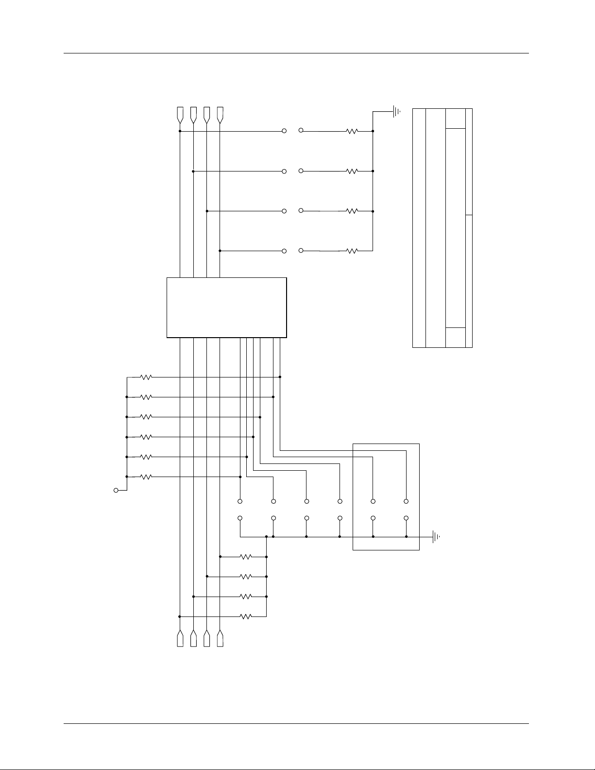
TMC2192 PRODUCT SPECIFICATION
AOUTAIN
5
20
AOUT
AIN
U9
1
24
R62
10K
DOUT
17
DOUT
DIN
13
8
COUT
CIN
12
BOUT
BOUT
BIN
A2X4C2X16B2X9D2X
21
NC17NC2
18
JP23
JUMPER
JP22
JUMPER
JP21
JUMPER
JP20
JUMPER
ST-163E
R48
R47
R46
R45
75
65-6294-34
75
ALL 1%
712Thursday, September 04, 1997
75
75
TMB2192 0.9.0
ST-163E
A
Title
Size Document Number Rev
Date: Sheet of
VCC
R61
R60
R59
R58
R57
10K
10K
10K
10K
10K
DIN
CIN COUT
A2XEN
JP14
BIN
JUMPER
R42 R43 R44
R41
DDDD
B2XEN
JP15
JUMPER
D IS150 OHM (1%)
Figure 31. ST-163E Layout
C2XEN
JP16
D2XEN
JUMPER
JP17
NC1EN
JUMPER
JP18
NC2EN
JUMPER
JP19
DO NOT STUFF
JUMPER
66 REV. 1.0.0 8/13/03
Page 67
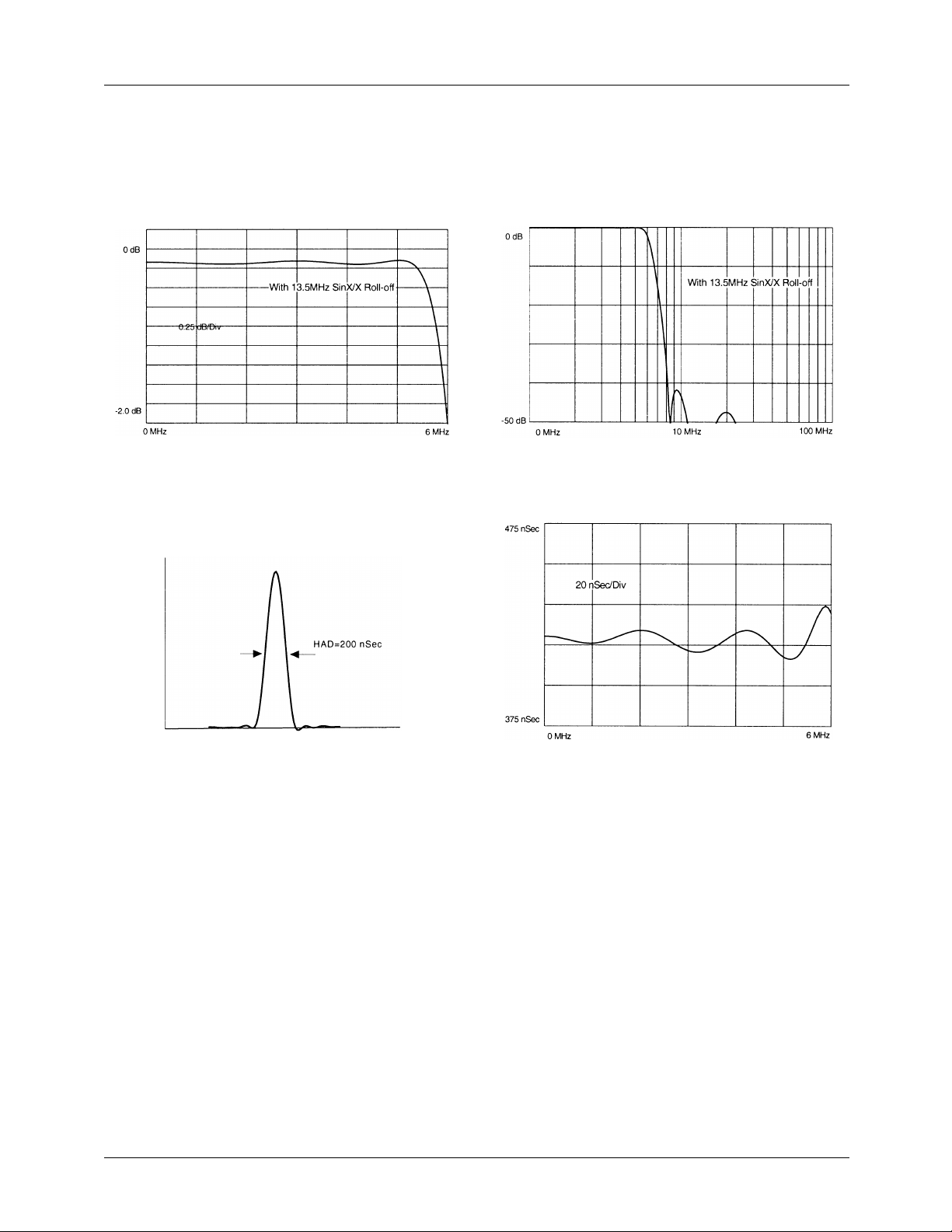
PRODUCT SPECIFICATION TMC2192
Output Low-Pass Filters
The response at 5.0MHz typically varies < ±0.25dB with
supplies of ±5V to ±8V. When operating in the 0dB gain
Figure 32. Pass Band
mode, pin 6 must be well isolated from ground planes. When
operating in the +6dB gain mode, pin 6 must have a low
resistance path to ground.
Figure 33. Stop Band
Figure 34. 2T Pulse Figure 35. Group Delay
REV. 1.0.0 8/13/03 67
Page 68
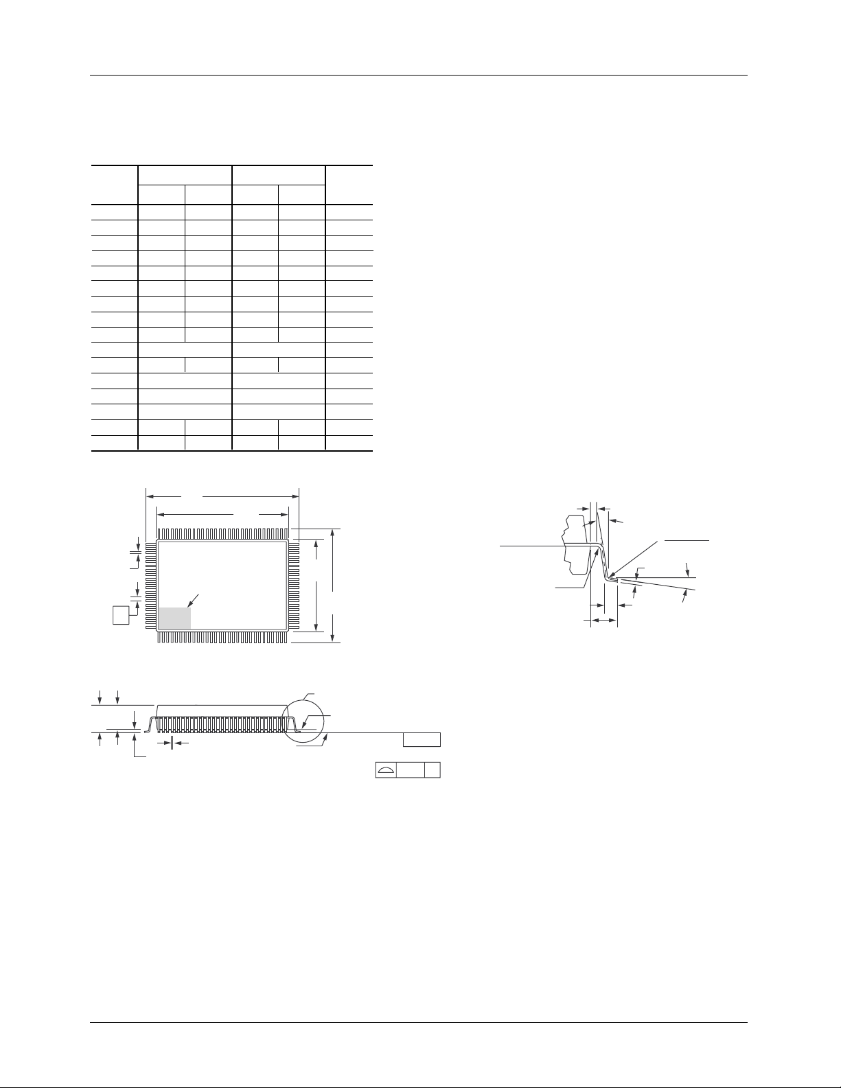
TMC2192 PRODUCT SPECIFICATION
Mechanical Dimensions
100-Lead MQFP
Symbol
A — .134 — 3.40
A1 .010 — .25 —
A2 .100 .120 2.55 3.05
B .008 3, 5
C .005 .13
D .904 .923 22.95 23.45
D1 .783 .791 19.90 20.10
E .667 .687 16.95 17.45
E1 .547 .555 13.90 14.10
e
L .028 .040 .73 1.03
N
ND
NE
α 0° 7° 0° 7°
ccc
Inches
Min. Max. Min. Max.
.015 .38
.009 .23
.0256 BSC .65 BSC
100 100
30 30
20 20
— .004 — .12
D
B
Pin 1 Indentifier
e
Millimeters
.22
D1
E1
Notes
E
Notes:
1.
All dimensions and tolerances conform to ANSI Y14.5M-1982.
2.
Controlling dimension is millimeters.
3.
Dimension "B" does not include dambar protrusion. Allowable
dambar protrusion shall be .08mm (.003in.) maximum in excess of
the "B" dimension. Dambar cannot be located on the lower radius
or the foot.
4.
5
4
"L" is the length of terminal for soldering to a substrate.
5.
"B" & "C" includes lead finish thickness.
.20 (.008) Min.
0° Min.
Datum Plane
.13 (.005) R Min.
0.076" (1.95mm) Ref
Lead Detail
L
.13 (.30)
.005 (.012)
C
R
α
See Lead Detail
AA2
A1
B
Seating Plane
Base Plane
-C-
Lead Coplanarity
ccc C
68 REV. 1.0.0 8/13/03
Page 69

TMC2192 PRODUCT SPECIFICATION
Ordering Information
Product Number Temperature Range Screening Package Package Marking
TMC2192KHC TA = 0°C to 70°C Commercial 100-pin MQFP TMC2192KHC
Life Support Policy
DISCLAIMER
FAIRCHILD SEMICONDUCTOR RESERVES THE RIGHT TO MAKE CHANGES WITHOUT FURTHER NOTICE TO
ANY PRODUCTS HEREIN TO IMPROVE RELIABILITY, FUNCTION OR DESIGN. FAIRCHILD DOES NOT ASSUME
ANY LIABILITY ARISING OUT OF THE APPLICATION OR USE OF ANY PRODUCT OR CIRCUIT DESCRIBED HEREIN;
NEITHER DOES IT CONVEY ANY LICENSE UNDER ITS PATENT RIGHTS, NOR THE RIGHTS OF OTHERS.
LIFE SUPPORT POLICY
FAIRCHILD’S PRODUCTS ARE NOT AUTHORIZED FOR USE AS CRITICAL COMPONENTS IN LIFE SUPPORT DEVICES
OR SYSTEMS WITHOUT THE EXPRESS WRITTEN APPROVAL OF THE PRESIDENT OF FAIRCHILD SEMICONDUCTOR
CORPORATION. As used herein:
1. Life support devices or systems are devices or systems
which, (a) are intended for surgical implant into the body,
or (b) support or sustain life, and (c) whose failure to
perform when properly used in accordance with
instructions for use provided in the labeling, can be
reasonably expected to result in a significant injury of the
user.
www.fairchildsemi.com
2. A critical component in any component of a life support
device or system whose failure to perform can be
reasonably expected to cause the failure of the life support
device or system, or to affect its safety or effectiveness.
8/13/03 0.0m 002
2003 Fairchild Semiconductor Corporation
Stock#DS30002192
 Loading...