

Page 1

www.fairchildsemi.com
TMC2250A
Matrix Multiplier
12 x 10 bit, 50 MHz
Features
• Four user-selectable filtering and transformation
functions:
– Triple dot product (3 x 3) matrix multiply
– Cascadeable 9-tap systolic FIR filter
– Cascadeable 3 x 3-pixel image convolver
– Cascadeable 4 x 2-pixel image convolver
• 50 MHz (20ns) pipelined throughput
• 12-bit input and output data, 10-bit coefficients
• 6-bit cascade input and output ports in all filter modes
• Onboard coefficient storage, with three-cycle updating of
all nine coefficients
Description
The TMC2250A is a flexible high-performance nine-multiplier
array VLSI circuit which can execute a cascadeable 9-tap
FIR filter, a cascadeable 4 x 2 or 3 x 3-pixel image convolution, or a 3 x 3 color space conversion. All configurations
offer throughput at up to the maximum guaranteed 50 MHz
clock rate with 12-bit data and 10-bit coefficients. All inputs
and outputs are registered on the rising edges of the clock.
The 3 x 3 matrix multiply or color conversion configuration
can perform video standard conversion (YIQ or YUV to
RGB, etc.) or three-dimensional perspective translation at
real-time video rates.
The 9-tap FIR filter configuration, useful in Video, Telecommunications, and Signal Processing, features a 16-bit cascade
input to allow construction of longer filters.
Applications
• Image filtering and manipulation
• Video effects generation
• Video standards conversion and encoding/decoding
• Three-dimensional image manipulation
• Medical image processing
• Edge detection for object recognition
• FIR filtering for communications systems
The cascadeable 3 x 3 and 4 x 2-pixel image convolver functions allow the user to perform numerous image processing
functions, including static filters and edge detectors. The 16-bit
cascade input port facilitates two-chip 50 MHz cubic convolution (4 x 4-pixel kernel).
The TMC2250A is fabricated in a sub-micron CMOS process
and operates at clock speeds of up to 50 MHz over the full
commercial (0°C to 70°C) temperature and supply voltage
ranges. It is available in 120-pin Plastic Pin Grid Array
(PPGA) packages, 120-lead Ceramic Pin Grid Array package (CPGA), 120-lead PQFP to PPGA package (MPGA) and
120-lead Plastic Quad FlatPack (PQFP). All input and output
signals are TTL compatible.
REV. 1.0.2 10/25/00
Page 2
PRODUCT SPECIFICATION TMC2250A
Functional Description
The TMC2250A is a nine-multiplier array with the internal bus
structure and summing adders needed to implement a 3 x 3
matrix multiplier (triple dot product) a cascadeable 9-tap FIR
filter, a 3 x 3-pixel convolver, or a 4 x 2-pixel convolver all in
one monolithic circuit. With a 50MHz guaranteed maximum
clock rate, this device offers video and imaging system
designers a single-chip solution to numerous common image
and signal-processing problems.
The three data input ports (A, B, C) accept 12-bit two's complement integer data, which is also the format for the output
ports (X, Y, Z) in the matrix multiply mode (Mode 00). In the
filter configurations (Modes 01, 10, and 11) the cascade ports
assume 12-bit integer, 4-bit fractional two's complement data
on both input and output. The coefficient input ports (KA,
KB, KC) are always 10-bit two's complement fractional.
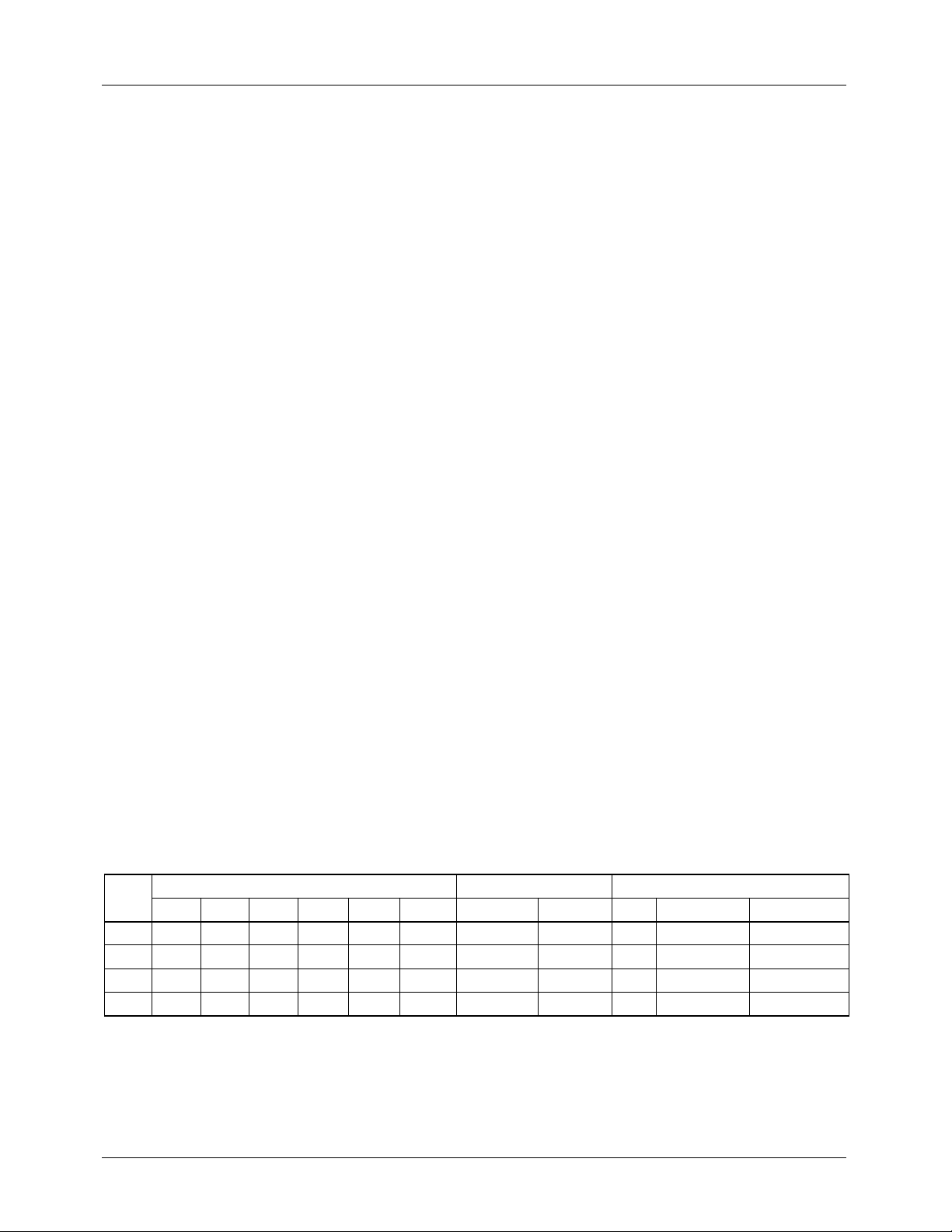
Table 1 details the bit weighting of the input and output data
in all configurations.
Operating Modes
The TMC2250A can implement four different digital filter
architectures. Upon selection of the desired function by the
user (MODE
), the device reconfigures its internal data
1-0
paths and input and output buses appropriately. The output
ports (XC, YC and ZC) are configured in all filter modes a
16-bit Cascade In and Cascade Out ports so that multiple
devices can be connected to build larger filters. These modes
are described individually below. The I/O function configurations for all four modes are shown in Table 1.
Definitions
The calculations performed by the TMC2250A in each mode
are also shown below, utilizing the following notation:
A(1), B(5), C(2), CASIN(3)
Indicates the data word presented to that input port during
the specified clock rising edge(x). Applies to all input ports
A
, B
, C
11-0
11-0
, and CASIN
11-0
15-0
.
KA1(1), KB3(4)
Indicates coefficient data stored in the specified one of the
nine onboard coefficient registers KA1 through KC3, as
shown in the block diagram for that mode, input during or
before the specified clock rising edge (x).
X(1), Y(4), Z(6), CASOUT (6)
Indicated data available at that output port t
after that
DO
specified clock rising edge (x). Applies to all output ports
X
, Y
, Z
11-0
11-0
, and CASOUT
11-0
15-0
.
Numeric Format
Table 2 shows the binary weightings of the input and output
ports of the TMC2250A. Although the internal sums of products could grow to 23 bits, in the matrix multiply mode
(Mode 00) the outputs X, Y and Z are rounded to yield 12-bit
integer words. Thus the output format is identical to the input
data format. In the filter configurations (Modes 01, 10, and
11) the cascade output is always half-LSB rounded to 16
bits, specifically 12 integer bits and 4 fractional guard bits,
with no overflow "headroom". The user is of course free to
half-LSB round the output word to any size less than 16 bits
by forcing a 1 into the bit position of the cascade input
immediately below the desired LSB. In all modes, bit
weighting is easily adjusted if desired by applying the same
scaling correction factor to both input and output data words.
If the coefficients are rescaled, the relative weightings of the
CASIN and CASOUT ports will differ accordingly.
Data Overflow
As shown in Table 2, the TMC2250A's matched input and
output data formats accommodate 0dB (unity) gain. Therefore, the user must be aware of input conditions that could
lead to numeric overflow. Maximum input data and coefficient word sizes must be taken into account with the specific
algorithm performed to ensure that no overflow occurs.
Table 1. Data Port Formatting by Mode
Mode
00 A
01 A
10 A
11 A
2
A
11-0
11-0
11-0
11-0
11-0
B
B
B
B
B
11-0
11-0
11-0
11-0
11-0
Inputs Inputs/Output Outputs
C
C
C
KA
11-0
KA
11-0
NC KA
KA
11-0
NC KA
9-0
9-0
9-0
9-0
9-0
KB
KB
KB
KB
KB
9-0
9-0
9-0
9-0
9-0
KC9-0 XC
KC9-0 X
11-0
KC9-0 CASIN
KC9-0 CASIN
KC9-0 CASIN
11-0
15-4
15-4
15-4
YC
11-8
Y
11-8
CASIN
CASIN
CASIN
Y
7-4
Y
7-4
NC CASOUT
3-0
NC CASOUT
3-0
NC CASOUT
3-0
YC3-0 ZC
Y
3-0
3-0
3-0
3-0
REV. 1.0.2 10/25/00
Z
CASOUT
CASOUT
CASOUT
11-0
11-0
15-4
15-4
15-4
Page 3

TMC2250A PRODUCT SPECIFICATION
Table 2. Bit Weightings for Input and Output Data Words
11
10
9
8
7
6
5
4
3
2
1
0
-1
-2
-3
-4
-5
-6
-7
Bit Weights 2
2
2
2
2
2
2
2
2
2
2
2
.2
2
2
2
2
2
Inputs
All Modes
-I
I
I
I
I
I
I
I
I
I
I
I
11
10
9
8
7
6
5
4
3
2
1
.
0
Data A, B, C
Coefficients
-K
9
.K
K
K
K
K
8
7
6
K
5
4
3
KA, KB, KC
Modes 01,
-CI
15
CI
CI
13CI12CI11CI10CI9CI8CI7CI6CI5CI4
14
.CI3CI2CI1CI
0
10, 11 CASIN
Internal Sum X20X19X18X17X16X15X14X13X12X11X10X9.X8X7X6X5X4X3X2X1X
Outputs
Mode 00
-O
11O10O9O8O7O6O5O4O3O2O1O0
.
X, Y, Z
Modes 01,
10, 11
CO
-
CO
CO
CO
CO
15
1
1
1
4
3
2
CO
1
1
1
0CO9CO8CO7CO6CO5
CO4.CO3CO2CO1CO
0
CASOUT
Note: A minus sign indicates a two’s complement sign bit.
-8
2
2
2
K
K
K
2
1
-9
0
0
REV. 1.0.2 10/25/00
3
Page 4
PRODUCT SPECIFICATION TMC2250A
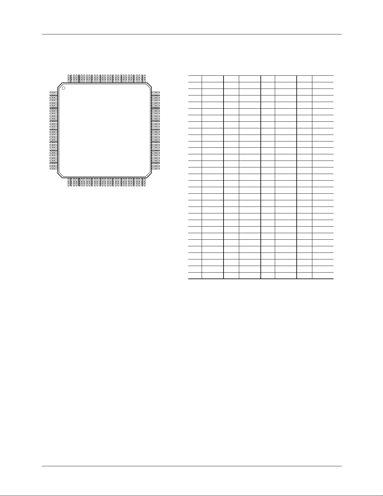
Pin Assignments
120 Pin Plastic Quad Flat Pack (MQFP), KE Package
Pin Name Pin Name
31
32
33
34
35
36
37
38
39
40
41
42
43
44
45
46
47
48
49
50
51
52
53
54
55
56
57
58
59
60
ZC
ZC
ZC
GND
ZC
ZC
ZC
KC
KC
KC
KC
GND
KC
KC
KC
V
KC
KC
KC
KB
KB
KB
KB
KB
KB
KB
KB
KB
KB
KA
XC
120 91
1
30
31 60
90
61
1
2
3
4
5
6
7
8
9
10
11
12
13
14
15
16
17
18
19
20
21
22
23
24
25
26
27
28
29
30
XC
XC
XC
XC
XC
XC
GND
YC
YC
YC
V
DD
YC
Y
7
Y
6
GND
Y
5
Y
4
YC
V
DD
YC
YC
YC
GND
ZC
ZC
ZC
ZC
ZC
ZC
6
5
4
3
2
1
0
11
10
9
8
0
1
2
3
0
1
2
3
4
5
Pin Name Pin Name
KA
61
DD
6
7
8
9
10
11
0
1
2
3
4
5
6
7
8
9
0
1
2
3
4
5
6
7
8
9
0
62
63
64
65
66
67
68
69
70
71
72
73
74
75
76
77
78
79
80
81
82
83
84
85
86
87
88
89
90
1
KA
2
KA
3
KA
4
KA
5
KA
6
KA
7
KA
8
KA
9
CWE
CWE
GND
A
0
A
1
A
2
A
3
A
4
A
5
A
6
A
7
A
8
A
9
A
10
A
11
B
0
B
1
B
2
CLK
B
3
B
4
1
0
91
92
93
94
95
96
97
98
99
100
101
102
103
104
105
106
107
108
109
110
111
112
113
114
115
116
117
118
119
120
B
5
B
6
B
7
B
8
B
9
B
10
B
11
C
0
C
1
C
2
C
3
V
DD
C
4
C
5
C
6
GND
C
7
C
8
C
9
C
10
C
11
MODE
MODE
GND
XC
11
XC
10
XC
9
V
DD
XC
8
XC
7
1
0
4 REV. 1.0.2 10/25/00
Page 5
TMC2250A PRODUCT SPECIFICATION
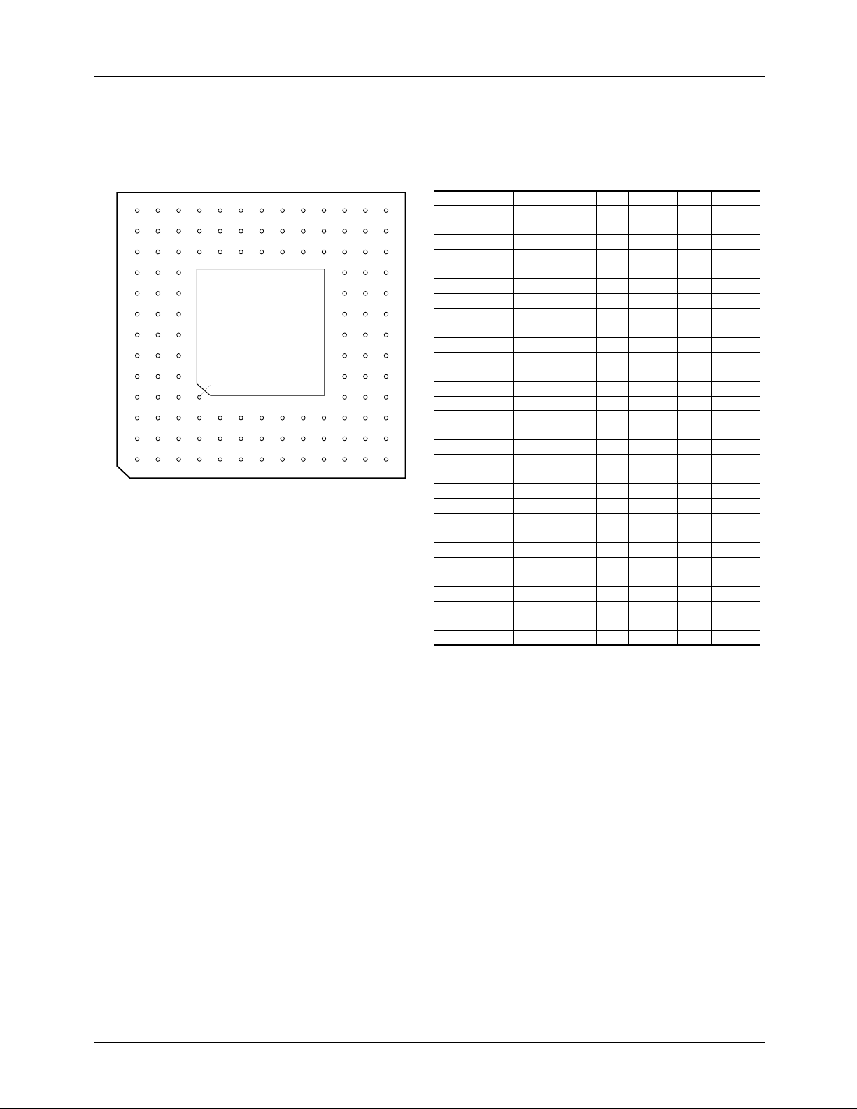
Pin Assignments (continued)
120 Pin Plastic Pin Grid Array, H5 Package and 120 Pin Ceramic Pin Grid Array, G1 Package and
120 Pin Plastic Quad Flatpack to 120-Pin Pin Grid Array (MPGA)
13
12
11
10
Pin Name Pin Name
C5
C6
C7
C8
C9
C10
C11
C12
C13
D1
D2
D3
D11
D12
D13
E1
E2
E3
E11
E12
E13
F1
F2
F3
F11
F12
F13
G1
G2
G3
GND
C
GND
V
DD
C
B
8
B
5
B
3
B
1
YC
XC
XC
CLK
B
0
A
10
YC
YC
GND
A
11
A
9
A
8
Y
7
YC
V
DD
A
7
A
6
A
5
Y
5
Y
6
GND
XC
A1
A2
A3
A4
A5
9
8
7
6
5
4
3
2
1
BADEFGHJKLMNC
Top View
Cavity Up
KEY
A6
A7
A8
A9
A10
A11
A12
A13
B1
B2
B3
B4
B5
B6
B7
B8
B9
B10
B11
B12
B13
C1
C2
C3
C4
7
XC
9
XC
10
MODE
C
11
C
8
C
7
C
5
C
3
C
1
B
10
B
7
B
4
XC
4
XC
5
XC
8
XC
11
MODE
C
9
C
6
C
4
C
2
B
11
B
9
B
6
B
2
XC
1
XC
2
XC
6
V
DD
0
1
Pin Name Pin Name
A
G11
3
A
G12
10
0
11
0
0
9
10
8
G13
H1
H2
H3
H11
H12
H13
J1
J2
J3
J11
J12
J13
K1
K2
K3
K11
K12
K13
L1
L2
L3
L4
L5
L6
L7
L8
L9
2
A
3
Y
4
YC
V
DD
GND
A
0
A
1
YC
YC
GND
KA
CWE
CWE
YC
ZC
ZC
KA
KA
KA
ZC
ZC
ZC
GND
KC
GND
V
DD
KB
KB
0
1
2
8
3
0
3
4
7
9
1
4
6
0
0
4
L10
KB
KA
KA
KA
ZC
ZC
ZC
ZC
KC
KC
KC
KC
KB
KB
KB
KA
KA
ZC
ZC
ZC
KC
KC
KC
KC
KC
KB
KB
KB
KB
KA
8
1
5
6
2
7
9
11
2
4
6
9
2
5
9
2
3
5
8
10
1
3
5
7
8
1
3
6
7
0
L11
L12
L13
M1
M2
M3
M4
M5
M6
M7
M8
M9
M10
1
M11
0
M12
M13
N1
N2
N3
N4
N5
N6
N7
N8
N9
N10
N11
N12
N13
REV. 1.0.2 10/25/00 5
Page 6
PRODUCT SPECIFICATION TMC2250A
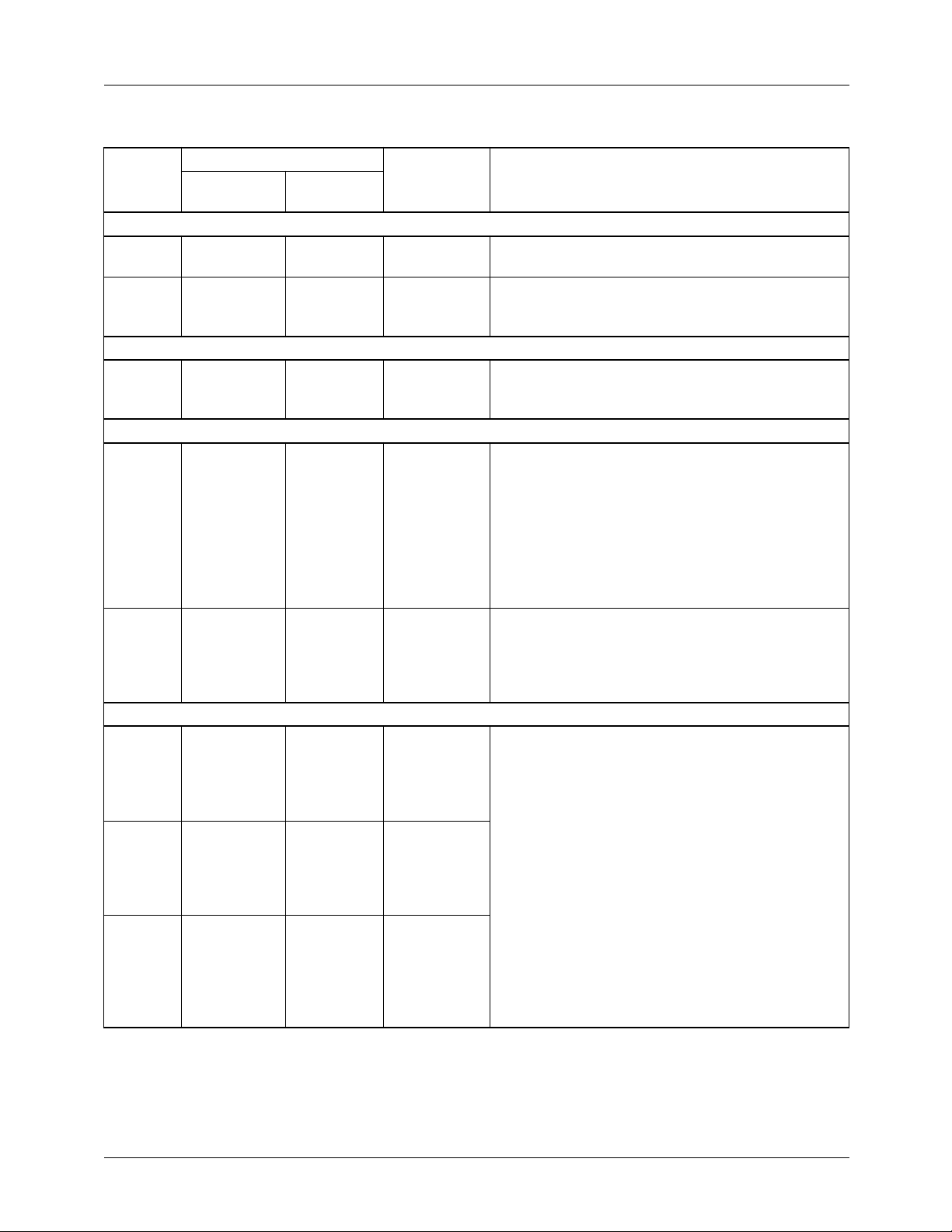
Pin Descriptions
Pin Number
Pin Name
Power
V
DD
GND E3, G3, J3, L4,
Clock
CLK D11 88 System Clock The TMC2250A operates from a single system clock
Controls
MODE
CPGA/PPGA/
MPGA
F3, H3, L7, C8, C412, 20, 46,
102, 118
8, 16, 24, 34,
L6, H11, C7,
1,0
C5
B4, A4 112, 113 Mode Control The TMC2250A will switch to the configuration
42, 72, 106,
MQFP
114
CWE
1,0
Input/Output
A
11-0
B
11-0
C
11-0
J12, J13 70, 71 Coefficient
E11, D13, E12,
E13, F11, F12,
F13, G13,
G11, G12,
H13, H12
B10, A11, B11,
C10, A12, B12,
C11, A13,
C12, B13,
C13, D12
A5, C6, B6, A6,
A7, B7, A8, B8,
A9, B9, A10,
C9
84, 83, 82, 81,
80, 79, 78, 77,
76, 75, 74, 73
97, 96, 95, 94,
93, 92, 91, 90,
89, 87, 86, 85
111, 110,
109, 108,
107, 105,
104, 103,
101, 100, 99,
98
Function Pin Description
Supply
Voltage
Ground The TMC2250A operates from a single +5V supply.
Write Enable
Data Input A Data presented to the 12-bit registered data input
Data Input B
Data Input C
The TMC2250A operates from a single +5V supply.
All pins must be connected.
All pins must be connected.
input. All timing specifications are referenced to the
rising edge of clock.
selected by the user (as shown in Table 3) on the
next clock. This registered control is usually static;
however, should the user wish to switch between
modes, the internal pipeline latencies of the device
must be taken into account. Valid data will not be
available at the outputs in the new configuration until
enough clocks in the new mode have passed to flush
the internal registers.
Data presented to the coefficient input ports (KA, KB,
and KC) will update three of the internal coefficient
storage registers, as indicated by the simultaneous
Coefficient Write Enable select, on the next clock.
See Table 4 and the Functional Block Diagram.
ports A, B, and C are latched into the multiplier input
registers for the currently selected configuration
(Table 3). In all modes except Mode 00, new data are
internally right-shifted to the next filter tap on each
rising edge of CLK.
6 REV. 1.0.2 10/25/00
Page 7
TMC2250A PRODUCT SPECIFICATION
Pin Descriptions (continued)
Pin Number
Pin Name
KA
9-0
CPGA/PPGA/
MPGA
K13, J11, K12,
L13, L12, K11,
M13, M12,
MQFP
69, 68, 67, 66,
65, 64, 63, 62,
61, 60
L11, N13
KB
9-0
M11, L10,
N12, N11,
M10, L9, N10,
59, 58, 57, 56,
55, 54, 53, 52,
51, 50
M9, N9, L8
KC
XC
9-0
11-0
M8, N8, N7,
M7, N6, M6,
N5, M5, N4, L5
B4, A3, A2, B3,
A1, C3, B2, B1,
D3, C2, C1, D2
49, 48, 47, 45,
44, 43, 41, 40,
39, 38
115, 116,
117, 119,
120, 1, 2, 3, 4,
5, 6, 7
YC
Y
YC
ZC
11-8
7-4
3-0
11-0
D1, E2, E1, F2 9, 10, 11, 13 CASIN
F1, G2, G1, H1 14, 15, 17, 18 Output
K1, J2, J1, H2 23, 22, 21, 19 CASOUT
M4, N3, M3,
N2, M2, L3,
N1, L2, K3,
37, 36, 35, 33,
32, 31, 30, 29,
28, 27, 26, 25
M1, L1, K2
Notes:
1. The output ports X, Y, Z and CASOUT, and input port CASIN are internally reconfigured by the device as required for each
mode of the device. The multiple-function pins have names which are combinations of these titles, as appropriate.
2. The output drivers on pins XC
power-up. If these pins are to be tied to other output drivers, to each other, or to ground or V
a clock pulse arrives within a few seconds of power-up, to avoid bus contention.
11-0
and YC
Function Pin Description
Coefficient
Input A1, A2,
A3
Data presented to the 10-bit registered coefficient
input ports KA, KB and KC are latched three at a time
into the internal coefficient storage register set
indicated by the Coefficient Write Enable CWE
Coefficient
the next clock, as shown in Table 4.
Input B1, B2,
B3
Coefficient
Input B1, B2,
B3
CASIN
Output X
15-4
/
In all modes except Mode 00, the x port and four bits
of the Y output port are reconfigured as the 16-bit
registered Cascade Input port CASIN
15-0
. Data
presented to this input will be added to the weighted
sums of the data words which were presented to the
/
3-0
Output Y
Output Y
11-0
7-4
3-0
CASOUT
Output Z
are not necessarily disabled until after the first rising edge of CLK following
11-8
11-0
input ports (A, B and C).
In the matrix multiply mode, data are available at the
only
12-bit registered output ports X, Y AND Z tDO after
every clock. These ports are reconfigured in the
/
3-0
filtering modes as 16-bit Cascade Input and Output
ports.CASOUT
/
15-4
In all modes except Mode 00, the Z port and four bits
15-0
of the Y output port are reconfigured as the 16-bit
registered Cascade Output port CASOUT
, the user should ensure that
DD
15-0
on
1,0
.
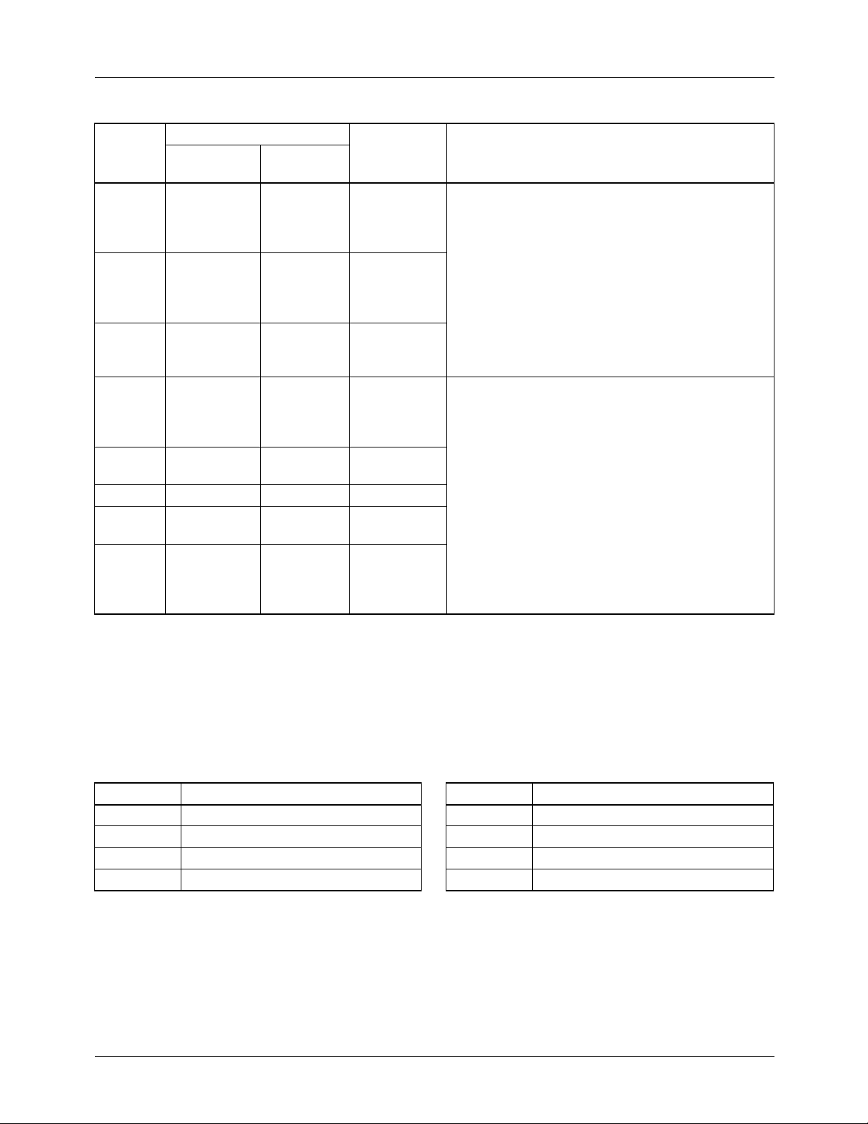
Table 3. Configuration Mode Word Table 4. Coefficient Write Enable Word
MODE
1,0
00 3 x 3 Matrix Multiply
01 9-Tap One Dimensional FIR
10 3 x 3 -Pixel Convolver
11 4 x 2 -Pixel Convolver
REV. 1.0.2 10/25/00 7
Configuration Mode
CWE
1,0
Coefficient Set Selected
00 Hold all registers
01 Update KA1, KB1, KC1
10 Update KA2, KB2, KC2
11 Update KA3, KB3, KC3
Page 8
PRODUCT SPECIFICATION TMC2250A
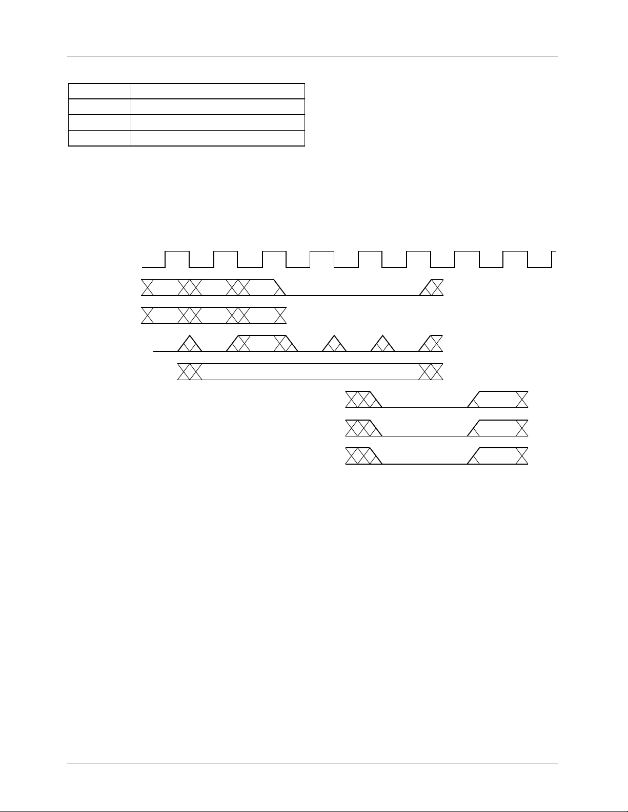
Table 5. Coefficient Input Ports
Input Port Registers Available
KA KA1, KA2, KA3
KB KB1, KB2, KB3
KC KC1, KC2, KC3
3 x 3 Matrix Multiplier (Mode 00)
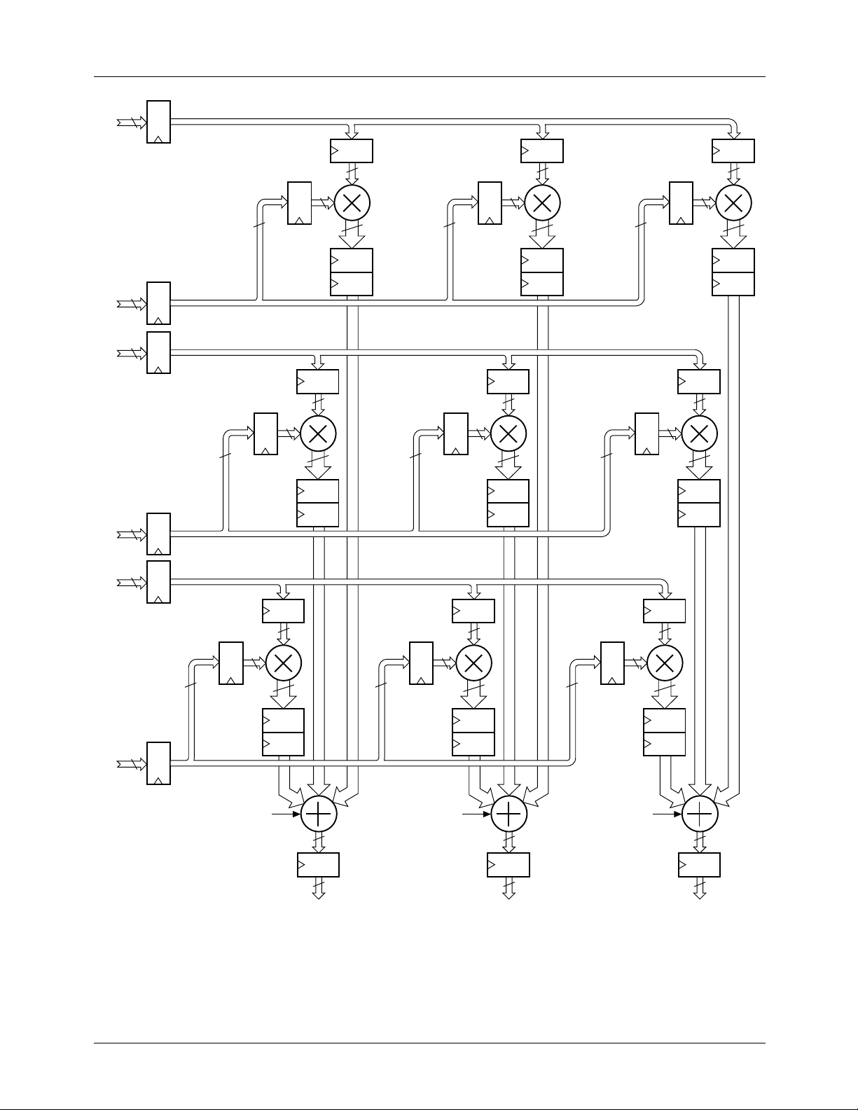
This mode utilizes all six input and output ports in the basic
configuration to realize a "triple dot product", in which each
output is the sum of all three input words in that column
CLK
CWE
KA, KB, KC
DATA IN A, B, C
1
01 10 11
K_1 K_2 K_3
0 0 1.0 0
2345678
multiplied by the appropriate stored coefficients. The three
corresponding sums of products are available at the outputs
five clock cycles after the input data are latched, and three
new data words half-LSB rounded to 12 bits are then available every clock cycle.
X(5)=A(1)KA1(1)+B(1)KB1(1)+C(1)KC1(1)
Y(5)=A(1)KA2(1)+B(1)KB2(1)+C(1)KC2(1)
Z(5)=A(1)KA3(1)+B(1)KB3(1)+C(1)KC3(1)
00
00
MODE CONTROL
X OUT
Y OUT
Z OUT
00
Figure 1. 3 x 3 Matrix Multiplier Impulse Response (Mode 00)
KA1 + KB1 + KC
KA2 + KB2 + KC
KA3 + KB3 + KC
1
2
3
8 REV. 1.0.2 10/25/00
Page 9
TMC2250A PRODUCT SPECIFICATION
KA
KB
12
10
12
10
1
222
12
KA1
10
10
1
222
KB1
10
10
3
4
12
21
21
3
4
10
10
KB2
10
KA2
10
3
4
12
21
12
KA3
10
10
10
KB3
10
3
4
21
3
4
12
21
3
4
12
21
A
B
KC
12
10
1
222
10
KC1
10
RND
12
KC2
10
21
3
4
12 (MSB)
5
12
X
10
RND
12
KC3
10
21
3
4
12 (MSB)
5
12
Y
10
RND
12
21
3
4
12 (MSB)
5
12
Z
C
Figure 2. 3 x 3 Matrix Multiplier Configuration (Mode 00)
REV. 1.0.2 10/25/00 9
Page 10
PRODUCT SPECIFICATION TMC2250A
9-Tap FIR Filter Mode (01)
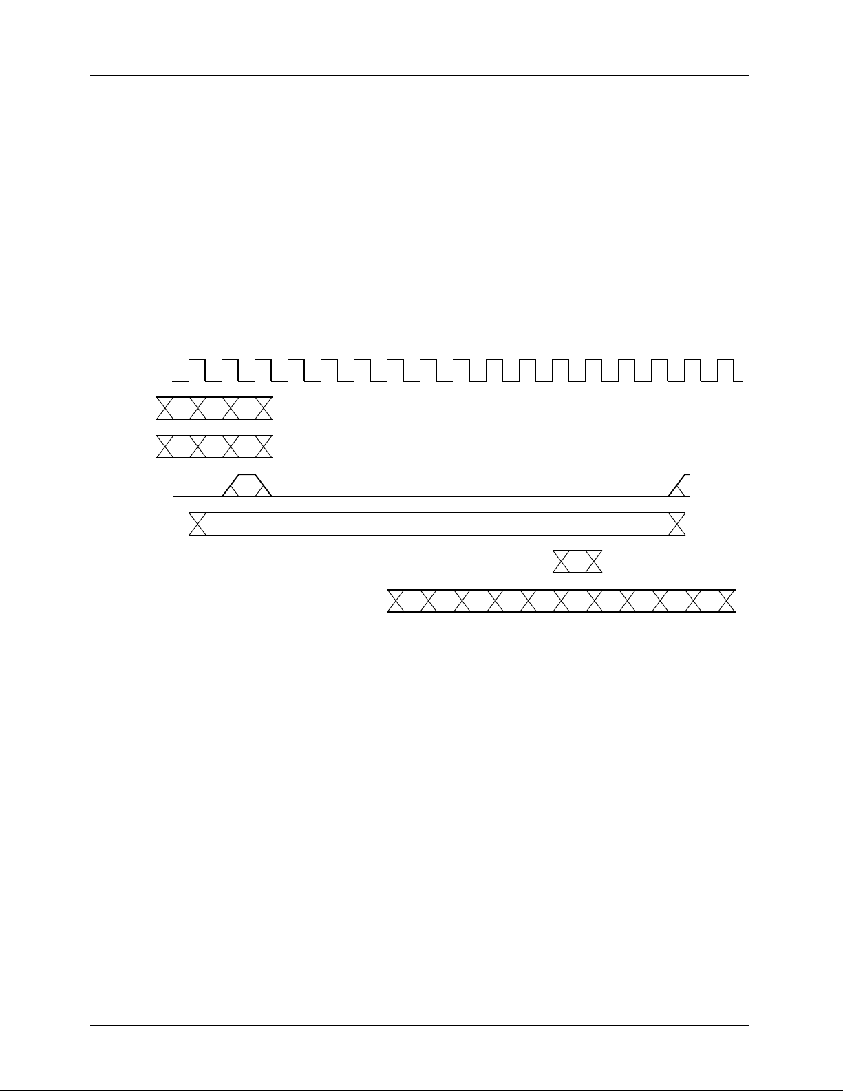
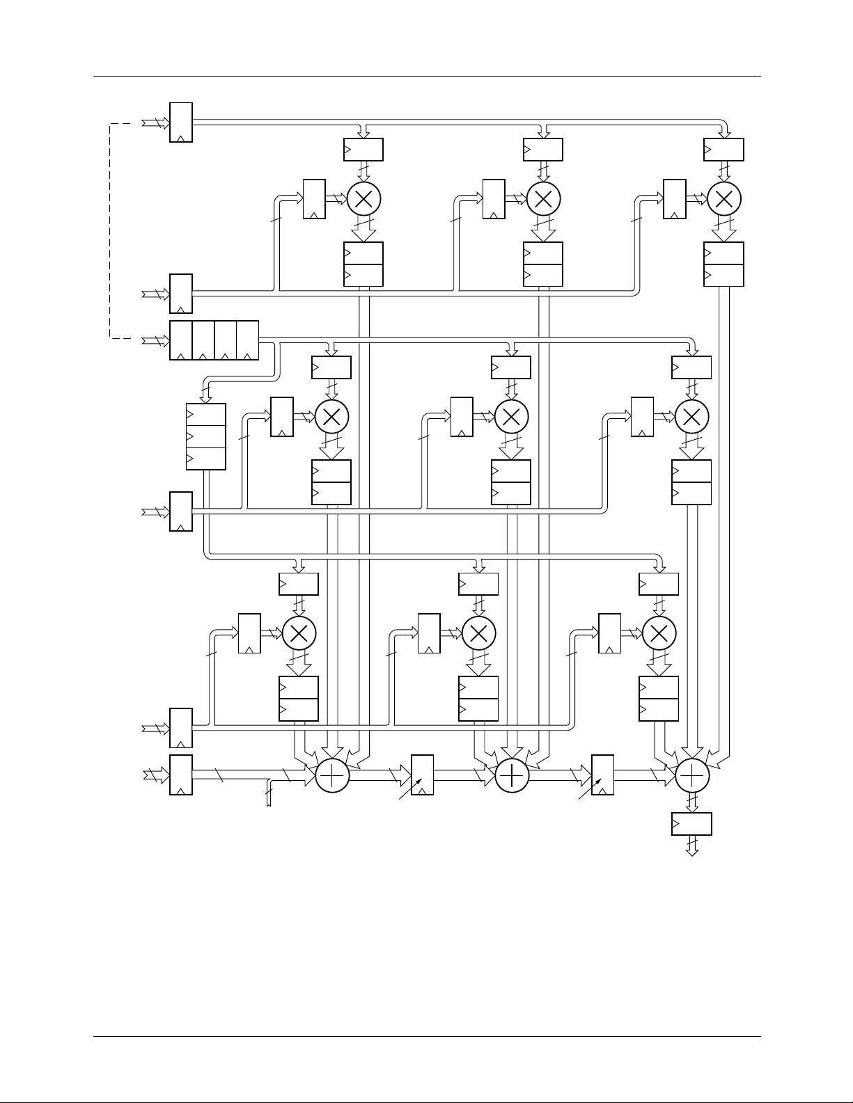
The architecture for this configuration is shown in Figure 4.
The user loads the desired coefficient set, presents input data
to ports A and B simultaneously (most applications will wire
the A and B inputs together), and receives the resulting 9sample response, half-LSB rounded to 16 bits, 5 to 13 clock
cycles later. A new output data word is available every clock
cycle.
The figure shows that the input data are automatically rightshifted by one position through the row of multiplier input
registers on every clock in anticipation of a new input data
word.
1
2 3 4 5 6 7 8 9 10 11 12 13 15 16 1714
CLK
CASOUT(13) =
A(9)KA3(9)+A(8)KA2(8)+A(7)KA1(7)
+B(6)KB3(9)+B(5)KB2(8)+B(4)KB1(7)
+B(3)KC3(9)+B(2)KC2(8)+B(1)KC1(7)
+CASIN(10)
Latency: Impulse in to center of 9-tap response =9 registers.
Cascade In to Cascade Out=4 registers.
CWE
KA, KB, KC
DATA IN A, B
MODE CONTROL
CASIN
CASOUT
01 10 11
K_1 K_2 K_3
1.0
01
KB
KB
KA
KA
KA
1
2
3
2
3
Figure 3. 9-Tap FIR Filter Impulse Response (Mode 01)
Q
KB
13
KC
1
2
3
13
1
Q
KC
KC
10 REV. 1.0.2 10/25/00
Page 11
TMC2250A PRODUCT SPECIFICATION
KA
KB
A
B
12
10
12
10
1
1 2 3 4
5
6
7
10
10
KB1
10
KA1
222
10
12
KA2
10
10
10
KB2
10
21
3
4
5
12
21
6
7
12
KA3
10
10
KB3
10
10
21
3
4
55
12
21
6
7
12
21
3
4
12
21
6
7
KC
CASIN
(0 - 15)
10
16
C
KC1
10
16 (MSB)
888
12
10
2, 5,
8, 11
KC2
10
10
21
9
10
21 21 21 21 21
5
‘10000’
HALF LSB
ROUNDING
10
12
21
9
10
3, 5, 6
8, 9, 11,
12
Figure 4. 9-Tap FIR Filter Configuration (Mode 01)
KC3
12
10
21
9
10
16 (MSB)
4 - 13
16
Z = CASOUT
(0 - 15)
REV. 1.0.2 10/25/00 11
Page 12
PRODUCT SPECIFICATION TMC2250A
3 x 3 Pixel Convolver (Mode 10)
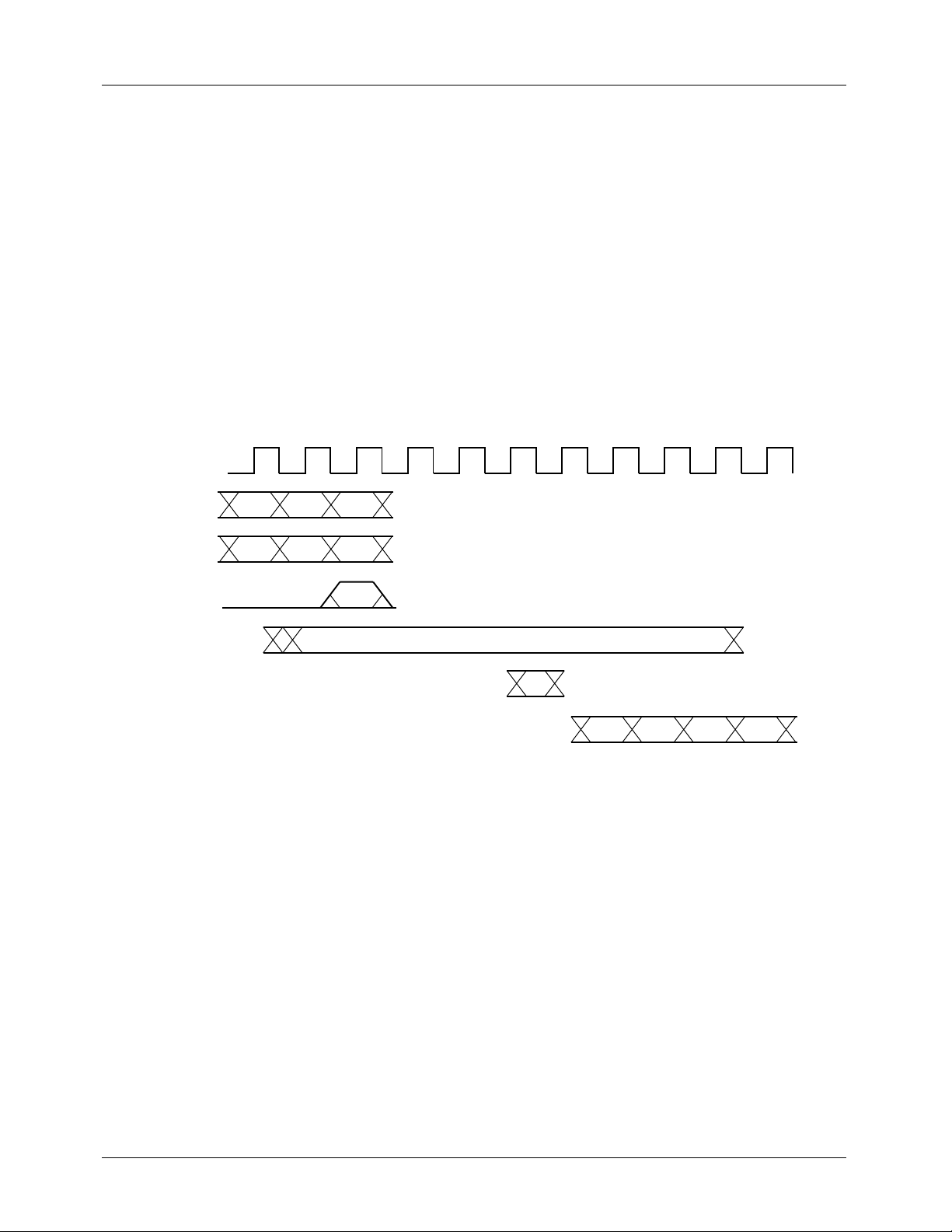
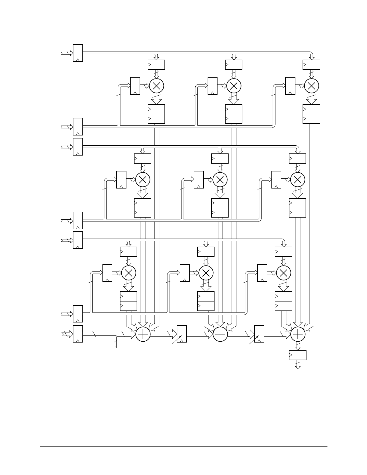
This filter configuration accepts a 3 pixel-square neighborhood, side-loaded three pixels at a time through input ports
A, B and C, and multiplies the 9 most recent pixel values by
the coefficient set currently stored in the registers. These
products are summed with the data presented to the cascade
input, and a new 3-cycle impulse response, rounded to 16
bits, is available at the output port 5 to 7 clocks later, with a
new output available on every clock cycle.
A(3)KA3(3)+A(2)KA2(2)+A(1)KA1(1)
+B(3)KB3(3)+B(2)KB2(2)+B(1)KB1(1)
+C(3)KC3(3)+C(2)KC2(2)+C(1)KC1(1)
CASOUT(7)=
+CASIN(4)
The input pixel data are automatically shifted one location to
the right through the three rows of multiplier input registers
on every clock in anticipation of three new input data words,
effectively sliding the convolutional window over one column in an image plane.
1
CLK
CWE
KA, KB, KC
DATA IN A, B, C
MODE 10
CASIN
CASOUT
01 10 11
K_1 K_2 K_3
234567891011
1.0
Latency: Impulse in to center of 3-tap response = 6 registers.
Cascade In to Cascade Out=4 registers.
01
Q
17
ΣK
ΣKj = KAj + KBj + KC
ΣK
3
2
ΣK
j
Q
1
7
Figure 5. 3 x 3-Pixel Convolver Impulse Response (Mode 10)
12 REV. 1.0.2 10/25/00
Page 13
TMC2250A PRODUCT SPECIFICATION
KA
KB
A
B
12
10
12
10
1
222
12
KA1
10
10
1
222
KB1
10
10
3
4
12
21
21
3
4
10
10
KB2
10
KA2
10
12
KA3
10
10
KB3
10
10
21
3
4
12
21
3
4
12
21
3
4
12
21
3
4
KC
CASIN
(0 - 15)
12
10
16
1
1
KC1
10
16 (MSB)
222
12
10
21
3
4
21 21 21 21 21
5
‘10000’
HALF LSB
ROUNDING
KC2
10
10
2, 5 3, 5, 6
12
21
3
4
10
KC3
12
10
21
3
4
16 (MSB)
4 - 7
16
Z = CASOUT
(0 - 15)
C
Figure 6. 3 x 3-Pixel Convolver Configuration (Mode 10)
REV. 1.0.2 10/25/00 13
Page 14
PRODUCT SPECIFICATION TMC2250A
4 x 2-Pixel Cascadeable Convolver
(Mode 11)
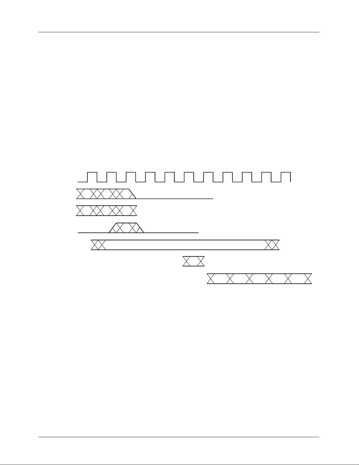
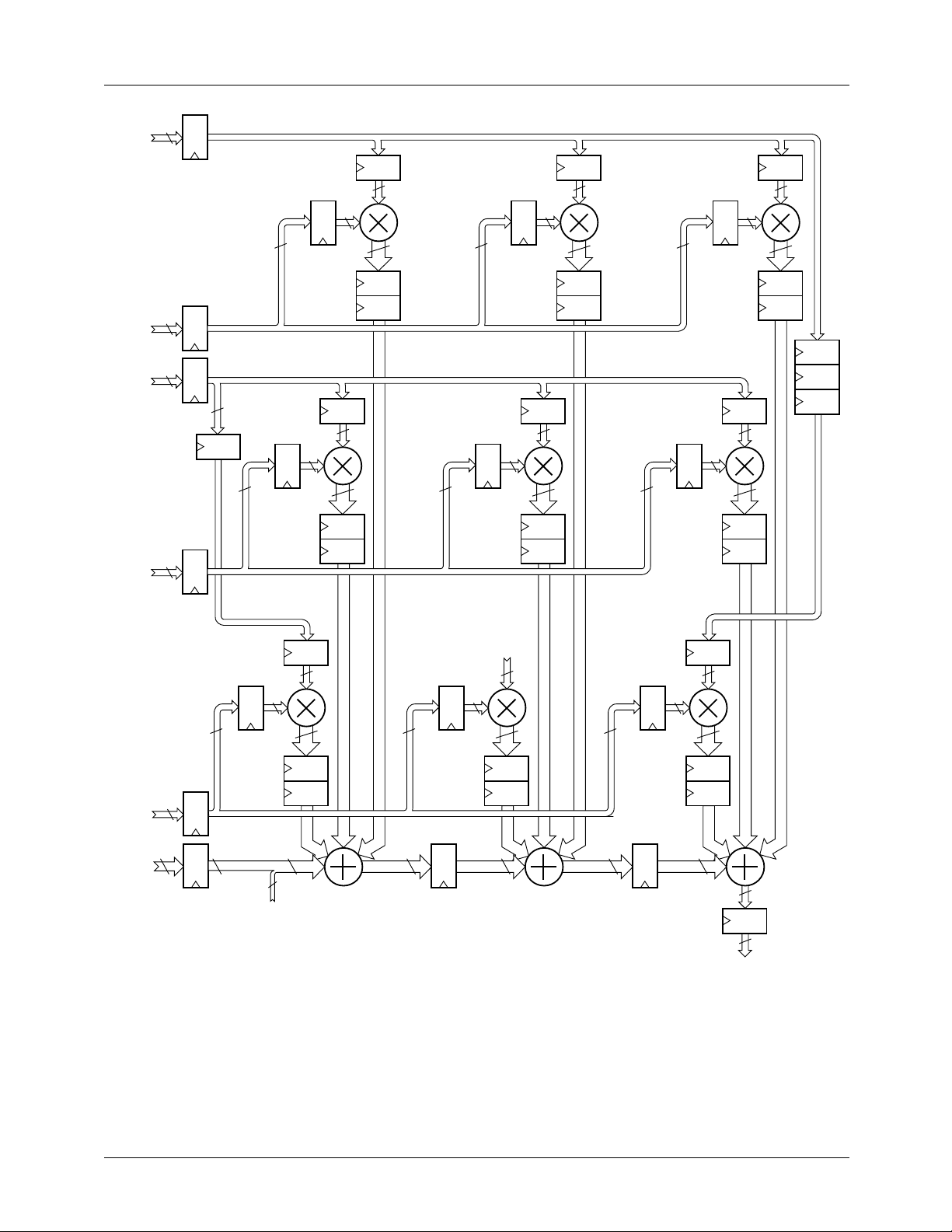
Similar to Mode 10, the 4 x 2 -Pixel convolver allows the use
to perform full-speed cubic convolution with only two
TMC2250A devices and the TMC2111A Pipeline Delay
Register to synchronize the cascade ports (see the Applications Discussion section).
As shown below, the column of input pixel data is automatically shifted one location to the right through the two rows of
multiplier input registers on every clock in anticipation of
two new input data words, effectively sliding the convolutional window over one column in an image plane.
Pixel data are side-loaded into ports A and B, multiplied by
the onboard coefficients, summed with the cascade input,
and half-LSB rounded to 16 bits. The four-cycle impulse
response emerges at the cascade output port 5 to 8 clock
cycles later. A new output word is available on every clock
cycle. Note that Multiplier KC2 is not used in this mode and
that its stored coefficient is ignored.
CLK
CWE
KA, KB, KC
DATA IN A, B
MODE
CASIN
CASOUT
1
01 10 11 00
K_1 K_2 K_3
234567891011
1.0
CASOUT(8)=
A(4)KA3(4)+A(3)KA2(3)+A(2)KA1(2)
+A(1)KB3(4)+B(4)KB3(4)+B(3)KB2(3)
+B(2)KB1(2)+B(1)KC1(2)+CASIN(5)
11
Q
8
KA3 + KB
3
KA2 + KB
KA1 + KB
2
1
KC1 + KC
Q
8
3
Figure 7. 4 x 2-Pixel Convolver Impulse Response (Mode 11)
14 REV. 1.0.2 10/25/00
Page 15
TMC2250A PRODUCT SPECIFICATION
KA
KB
A
B
12
10
12
10
1
222
12
KA1
10
10
1
2
2
KB1
10
222
10
3
4
12
21
21
3
4
10
10
KB2
10
KA2
10
12
KA3
10
10
KB3
10
10
21
3
4
12
21
3
4
12
21
3
4
2
3
4
12
21
3
4
KC
CASIN
(0 - 15)
10
16
C
1
KC1
10
16 (MSB)
HALF LSB
ROUNDING
10
0
12
KC3
21
10
3, 5,
6, 7
3
12
10
21
4
5
21 21 21 21 21
5
‘10000’
KC2
10
2, 5
6
Figure 8. 4 x 2-Pixel Convolver Configuration (Mode 11)
5
12
10
21
6
7
16 (MSB)
4 - 8
16
Z = CASOUT
(0 - 15)
REV. 1.0.2 10/25/00 15
Page 16
PRODUCT SPECIFICATION TMC2250A
t
CLK
CY
1
234 5
t
PWH
CWE
KA, KB, KC
X, Y, Z
CASOUT
tSt
H
PREVIOUS NEW
t
HO
t
PWL
t
D
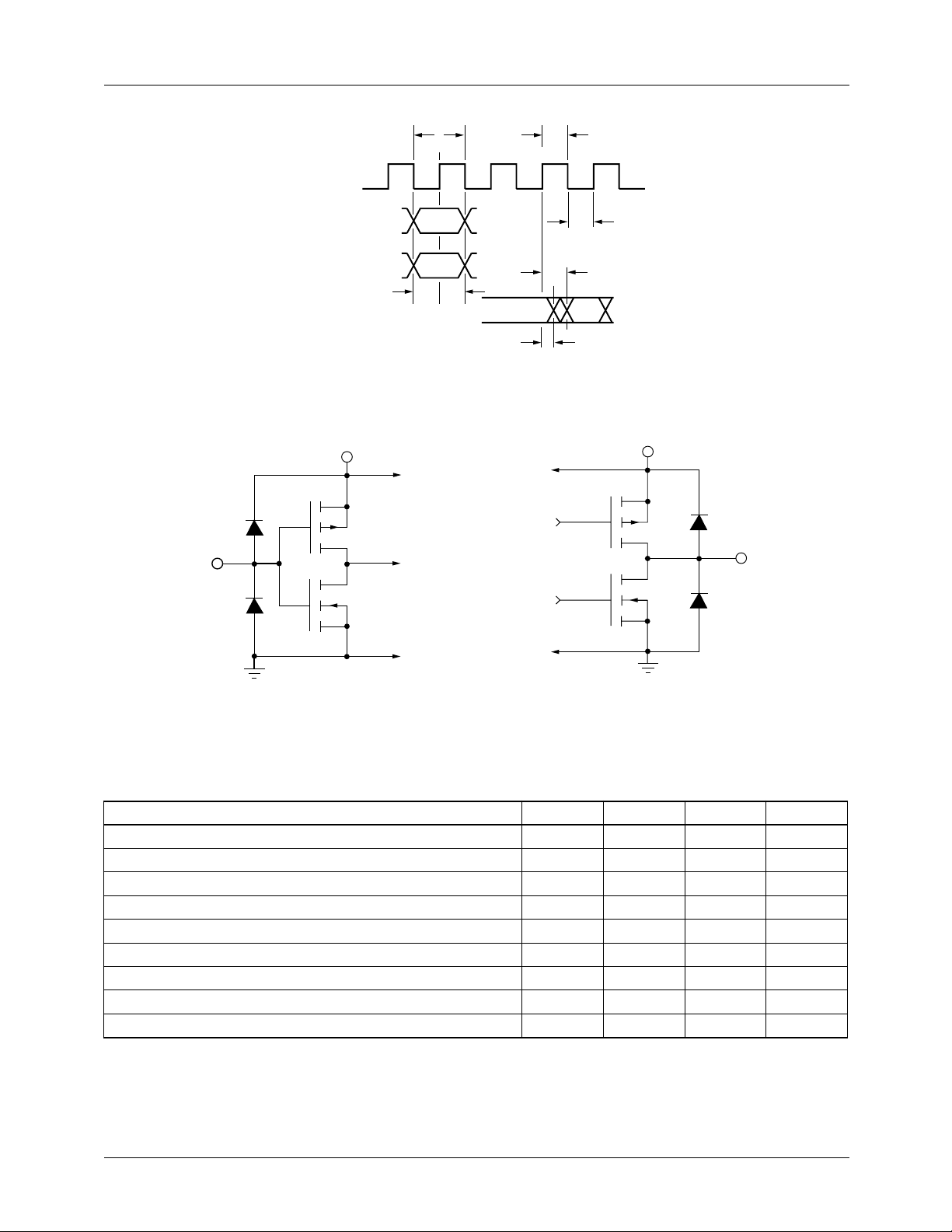
Figure 9. Input/Output Timing Diagram
V
V
DD
p
Digital
Input
n
DD
p
Digital
Output
n
GND
Figure 10. Equivalent Digital Input Circuit
Figure 11. Equivalent Digital Output Circuit
GND
Absolute Maximum Ratings (beyond which the device may be damaged)1
Parameter Min Typ Max Unit
Supply Voltage -0.5 7.0 V
Input Voltage -0.5 VDD + 0.5 V
Applied Voltage
Externally Forced Current
Short Circuit Duration (single output in HIGH state to ground) 1 sec
Operating, Ambient Temperature -20 110 °C
Junction Temperature 140 °C
Storage Temperature -65 150 °C
Lead Soldering Temperature (10 seconds) 300 °C
Notes:
1. Functional operation under any of these conditions is NOT implied. Performance and reliability are guaranteed only if
Operating Conditions are not exceeded.
2. Applied voltage must be current limited to specified range.
3. Forcing voltage must be limited to specified range.
4. Current is specified as conventional current flowing into the device.
2
3,4
-0.5 VDD + 0.5 V
-3.0 6.0 mA
16 REV. 1.0.2 10/25/00
Page 17
TMC2250A PRODUCT SPECIFICATION
Operating Conditions
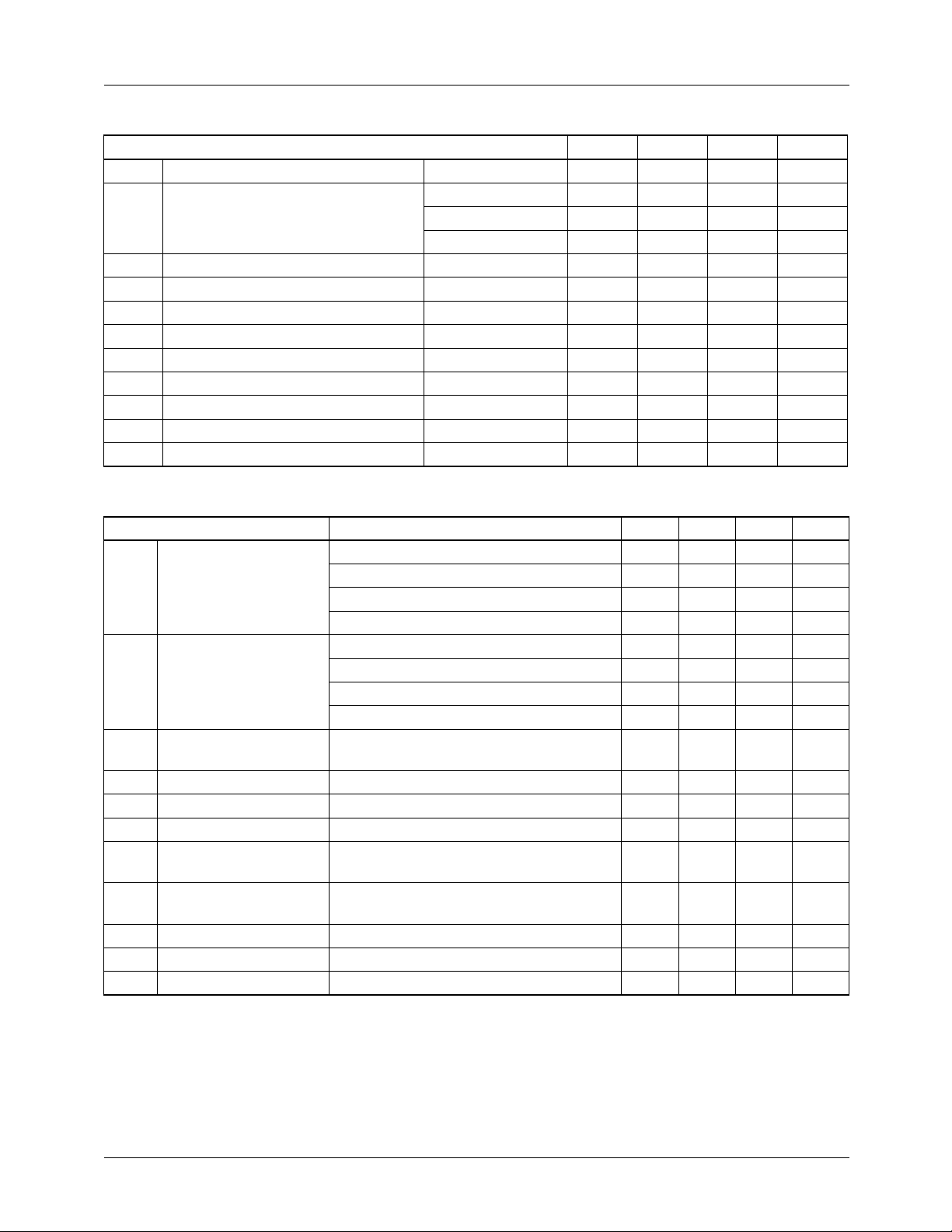
Parameter Min Nom Max Units
V
f
CLK
DD
Power Supply Voltage 4.75 5.0 5.25 V
Clock Frequency TMC2250A 30 MHz
TMC2250A-2 40 MHz
TMC2250A-3 50 MHz
t
PWH
t
PWL
t
S
t
H
V
IH
V
IL
I
OH
I
OL
T
A
CLK pulse width, HIGH 6 ns
CLK pulse width, LOW 8 ns
Input Data Setup Time 6 ns
Input Data Hold Time 2 ns
Input Voltage, Logic HIGH 2.0 V
Input Voltage, Logic LOW 0.8 V
Output Current, Logic HIGH -2.0 mA
Output Current, Logic LOW 4.0 mA
Ambient Temperature, Still Air 0 70 °C
Electrical Characteristics
Parameter Conditions Min Typ Max Units
I
DD
Total Power Supply
Current
VDD = Max, C
LOAD
= 25pF, f
CLK
= Max
TMC2250A 125 mA
TMC2250A-2 140 mA
TMC2250A-3 155 mA
I
DDU
Power Supply Current,
Unloaded
VDD = Max, OE = HIGH, f
CLK
=Max
TMC2250A 120 mA
TMC2250A-2 135 mA
TMC2250A-3 150 mA
I
DDQ
Power Supply Current,
VDD = Max, CLK = LOW 12 mA
Quiescent
C
I
IH
I
IL
I
OZH
I
OZL
I
OS
V
V
Notes:
1. Except pins XC
2. Pins XC
I/O Pin Capacitance 5 pF
PIN
Input Current, HIGH
Input Current, LOW
Hi-Z Output Leakage
Current, Output HIGH
Hi-Z Output Leakage
Current, Output LOW
1
VDD = Max, VIN = V
1
VDD = Max, V
VDD = Max, VIN = V
2
VDD = Max, VIN = 0 V ±10 µA
2
DD
= 0 V ±5 µA
IN
DD
Short-Circuit Current -20 -80 mA
Output Voltage, HIGH IOH = Max, VDD = Min 2.4 V
OH
Output Voltage, LOW IOL = Max, VDD = Min 0.4 V
OL
11-0
, YC
11-0
11-8
, YC
.
11-8
.
±5 µA
±10 µA
REV. 1.0.2 10/25/00 17
Page 18
PRODUCT SPECIFICATION TMC2250A
Switching Characteristics
Parameter Conditions Min Typ Max Units
t
t
DO
HO
Output Delay Time C
Output Hold Time C
= 25 pF 15 ns
LOAD
= 25 pF 3 ns
LOAD
Application Notes
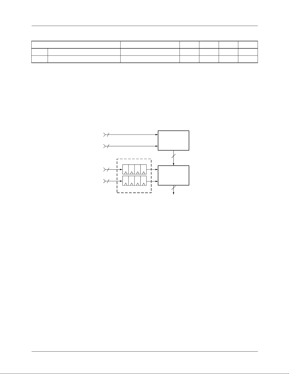
Performing Large-Kernel Pixel Interpolation
The Cascade Input and Output Ports of the TMC2250A allow the user to stack multiple devices to perform larger interpolation
kernels with no decrease in pixel throughput. Figure 12 illustrates a basic application utilizing Mode 11 to realize a 4 x 4-pixel
kernel, also called Cubic Convolution. This example utilizes the TMC2011A Variable-Length Shift Register to compensate for
the internal latency of each TMC2250A. Alternatively, some applications may utilize RAM, FIFO's, or other methods to store
multiple-line pixel data. In these cases the user may compensate for latency by simply offsetting the access sequencing of the
storage devices.
Figure 12. Figure 12. Performing Cubic Convolution with Two TMC2250A's
Related Products
• TMC2301 Image Resampling Sequencer
• TMC2302A Image Manipulation Sequencer
• TMC2249A Video Mixer
• TMC2242B Half-Band Filter
A
12
B
12
C
12
D
12
3 X TMC2111A
A
4 X 2 TMC2250A
B
CASOUT
16
CASIN
A
4 X 2 TMC2250A
B
CASOUT
16
OUTPUT
18 REV. 1.0.2 10/25/00
Page 19
TMC2250A PRODUCT SPECIFICATION
Mechanical Dimensions
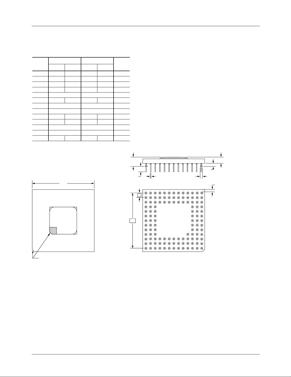
120-Lead CPGA Package
Symbol
A .080 .160 2.03 4.06
A1 .040 .060 1.01 1.53
A2 .125 3.17
øB .016 .020 0.40 0.51
øB2
D 1.340 1.380 33.27 35.05
D1
e
L
L1 .170 .190 4.31 4.83
M13 13
N
P
Inches
Min. Max. Min. Max.
.215 5.46
.050 NOM. 1.27 NOM.
1.200 BSC 30.48 BSC
.100 BSC 2.54 BSC
.110 .145 2.79 3.68
120 120
.003 — .076 —
D
Millimeters
Notes
2
2
SQ
3
4
A2
Notes:
1.
Pin #1 identifier shall be within shaded area shown.
2.
Pin diameter excludes solder dip finish.
3.
Dimension "M" defines matrix size.
4.
Dimension "N" defines the maximum possible number of pins.
5.
Orientation pin is at supplier's option.
6.
Controlling dimension: inch.
A1
L
e
øB
øB2
P
A
Top View
Cavity Up
Pin 1 Identifier
D1
REV. 1.0.2 10/25/00 19
Page 20
PRODUCT SPECIFICATION TMC2250A
Mechanical Dimensions
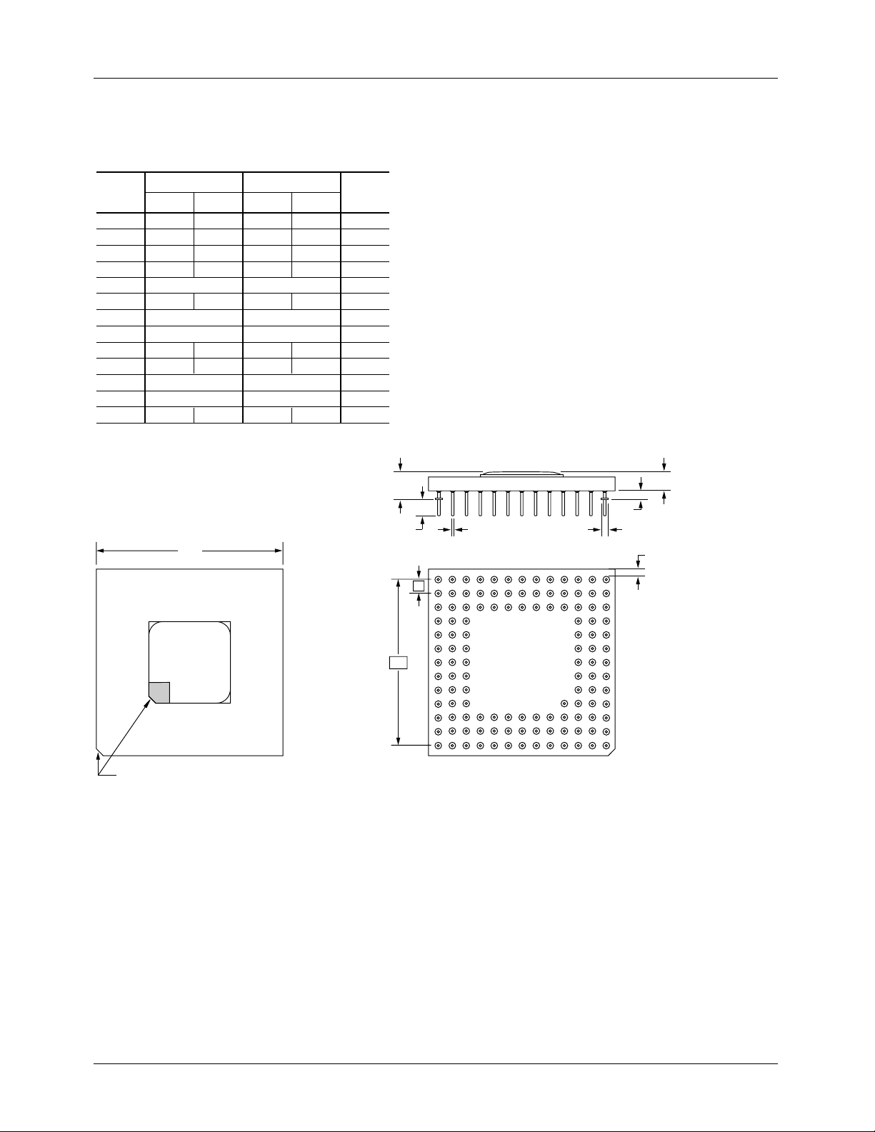
120-Lead PPGA Package
Symbol
A .080 .160 2.03 4.06
A1 .040 .060 1.01 1.53
A2 .125 3.17
øB .016 .020 0.40 0.51
øB2
D 1.340 1.380 33.27 35.05
D1
e
L
L1 .170 .190 4.31 4.83
M13 13
N
P
Inches
Min. Max. Min. Max.
.215 5.46
.050 NOM. 1.27 NOM.
1.200 BSC 30.48 BSC
.100 BSC 2.54 BSC
.110 .145 2.79 3.68
120 120
.003 — .076 —
D
Millimeters
Notes
2
2
SQ
3
4
A2
Notes:
1.
Pin #1 identifier shall be within shaded area shown.
2.
Pin diameter excludes solder dip finish.
3.
Dimension "M" defines matrix size.
4.
Dimension "N" defines the maximum possible number of pins.
5.
Orientation pin is at supplier's option.
6.
Controlling dimension: inch.
A1
L
e
øB
øB2
P
A
Top View
Cavity Up
Pin 1 Identifier
D1
20 REV. 1.0.2 10/25/00
Page 21
TMC2250A PRODUCT SPECIFICATION
Mechanical Dimensions
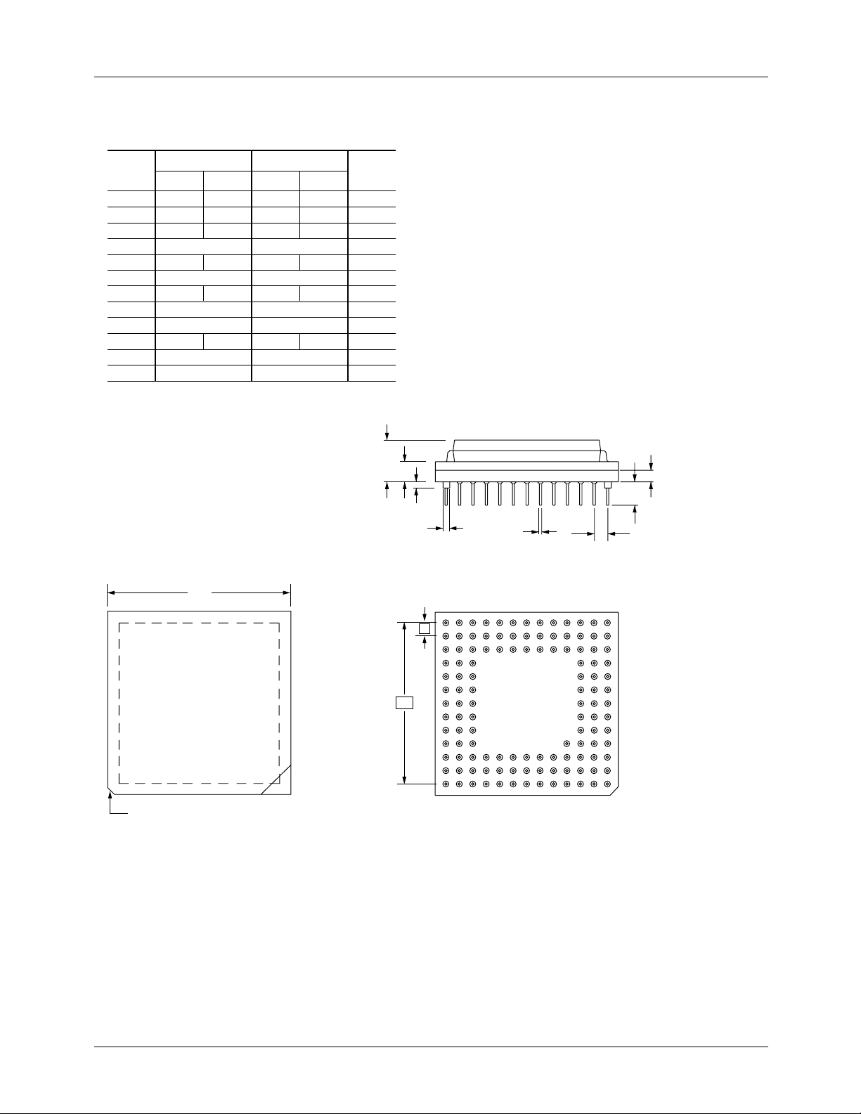
120-Lead Metric Quad Flat Package to Pin Grid Array Package (MPGA)
A1
Notes:
1.
Pin #1 identifier shall be within shaded area shown.
2.
Pin diameter excludes solder dip finish.
3.
Dimension "M" defines matrix size.
4.
Dimension "N" defines the maximum possible number of pins.
5.
Orientation pin is at supplier's option.
6.
Controlling dimension: inch.
L
A3
A2
Symbol
A .309 .311 7.85 7.90
A1 .145 .155 3.68 3.94
A2
A3
øB .016 .020 0.40 0.51
øB2
D 1.355 1.365 34.42 34.67
D1
e
L
M13 13
N
Inches
Min. Max. Min. Max.
.080 2.03
.175 .185 4.45 4.70
.090 2.29
.050 TYP. 1.27 TYP.
.050 NOM. 1.27 NOM.
1.200 BSC 30.48 BSC
.100 BSC 2.54 BSC
120 120
Millimeters
Notes
2
2
SQ
3
4
A
Fairchild
TMC2250A
Pin 1 Identifier
øB2
D
e
D1
øB
e
REV. 1.0.2 10/25/00 21
Page 22
PRODUCT SPECIFICATION TMC2250A
Mechanical Dimensions
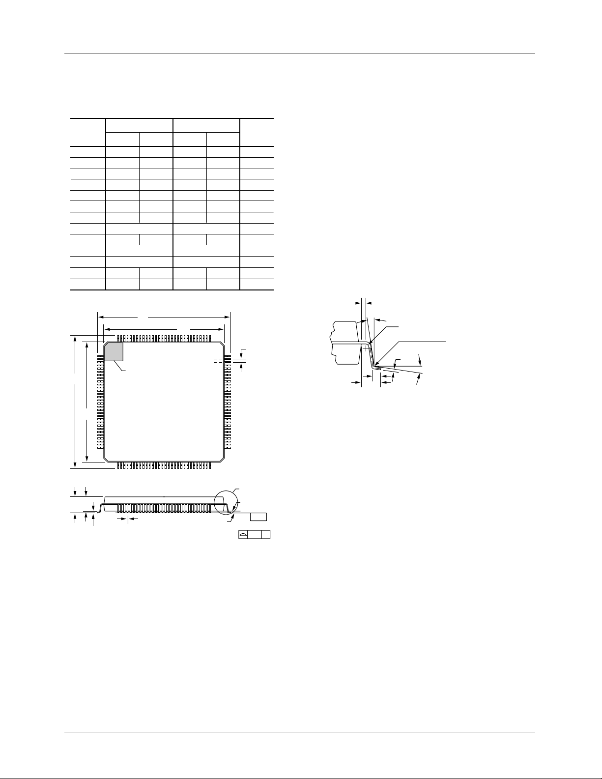
120-Lead MQFP Package
Symbol
A — .154 — 3.92
A1 .010 — .25 —
A2 .125 .144 3.17 3.67
B .012 3, 5.30
C .005 .13
D/E 1.219 1.238 30.95 31.45
D1/E1 1.098 1.106 27.90 28.10
e
L .026 .037 .65 .95
N
ND
α 0° 7° 0° 7°
ccc
E
E1
Inches
Min. Max. Min. Max.
.018 .45
.009 .23
.0315 BSC .80 BSC
120 120
30 30
— .004 — .10
D
PIN 1 IDENTIFIER
Millimeters
D1
Notes
5
4
e
0.063" Ref (1.60mm)
Notes:
1.
All dimensions and tolerances conform to ANSI Y14.5M-1982.
2.
Controlling dimension is millimeters.
3.
Dimension "B" does not include dambar protrusion. Allowable
dambar protrusion shall be .08mm (.003in.) maximum in excess
of the "B" dimension. Dambar cannot be located on the lower
radius or the foot.
4.
"L" is the length of terminal for soldering to a substrate.
5.
"B" & "C" includes lead finish thickness.
.20 (.008) Min.
0° Min.
.13 (.005) R Min.
.13/.30
.005/.012
C
L
Lead Detail
R
α
See Lead Detail
A2
A
B
A1
Seating Plane
Base Plane
-C-
LEAD COPLANARITY
ccc
C
22 REV. 1.0.2 10/25/00
Page 23

PRODUCT SPECIFICATION TMC2250A
Ordering Information
Product Number
Temperature
Range
Speed
Grade
Screening Package
Package
Marking
TMC2250AG1C 0°C to 70°C 30 MHz Commercial 120 Pin Ceramic Pin Grid Array 2250AG1C
TMC2250AG1C2 0°C to 70°C 40 MHz Commercial 120 Pin Ceramic Pin Grid Array 2250AG1C2
TMC2250AG1C3 0°C to 70°C 50 MHz Commercial 120 Pin Ceramic Pin Grid Array 2250AG1C3
TMC2250AH5C 0°C to 70°C 30 MHz Commercial 120 Pin Plastic Pin Grid Array 2250AH5C
TMC2250AH5C2 0°C to 70°C 40 MHz Commercial 120 Pin Plastic Pin Grid Array 2250AH5C2
TMC2250AH5C3 0°C to 70°C 50 MHz Commercial 120 Pin Plastic Pin Grid Array 2250AH5C3
TMC2250AH6C 0°C to 70°C 30 MHz Commercial 120 Lead Metric Quad Flatpack
N/A
to Pin Grid Array
TMC2250AH6C2 0°C to 70°C 40 MHz Commercial 120 Lead Metric Quad Flatpack
N/A
to Pin Grid Array
TMC2250AH6C3 0°C to 70°C 50 MHz Commercial 120 Lead Metric Quad Flatpack
N/A
to Pin Grid Array
TMC2250AKEC 0°C to 70°C 30 MHz Commercial 120 Lead Plastic Quad Flatpack 2250AKEC
TMC2250AKEC2 0°C to 70°C 40 MHz Commercial 120 Lead Plastic Quad Flatpack 2250AKEC2
TMC2250AKEC3 0°C to 70°C 50 MHz Commercial 120 Lead Plastic Quad Flatpack 2250AKEC3
LIFE SUPPORT POLICY
FAIRCHILD’S PRODUCTS ARE NOT AUTHORIZED FOR USE AS CRITICAL COMPONENTS IN LIFE SUPPORT DEVICES
OR SYSTEMS WITHOUT THE EXPRESS WRITTEN APPROVAL OF THE PRESIDENT OF FAIRCHILD SEMICONDUCTOR
CORPORATION. As used herein:
1. Life support devices or systems are devices or systems
which, (a) are intended for surgical implant into the body, or
(b) support or sustain life, and (c) whose failure to perform
when properly used in accordance with instructions for use
provided in the labeling, can be reasonably expected to
result in a significant injury of the user.
www.fairchildsemi.com
2. A critical component in any component of a life support
device or system whose failure to perform can be
reasonably expected to cause the failure of the life support
device or system, or to affect its safety or effectiveness.
10/25/00 0.0m 002
2000 Fairchild Semiconductor Corporation
Stock#DS30002250A
 Loading...