

TMC57253
DRIVER
SOCS040A – MARCH 1994 – REVISED NOVEMBER 1994
Copyright 1994, Texas Instruments Incorporated
1
POST OFFICE BOX 655303 • DALLAS, TEXAS 75265
• TTL-Compatible Inputs
• CCD-Compatible Outputs
• Adjustable Clock Levels
• High-Speed Clear
• Serial-Gate Midlevel for CDS Operation
• Solid-State Reliability
description
The TMC57253 is a monolithic CMOS integrated
circuit designed to drive image-area gates (IAG1,
IAG2), antiblooming gate (ABG), storage-area
gate (SAG), and serial-register gate (SRG) of the
Texas Instruments (TI) TC255 CCD image
sensor. The TMC57253 interfaces the CCD image
sensor to the TI TMC57751 ASIC or user-defined
timing generator; it receives TTL-input signals
from the timing generator and outputs levelshifted signals to the image sensor.
ABOUT follows ABIN and ABMIN and switches
between V
ABL
, VAB, and V
ABM
. IA1OUT and
IA2OUT follow IA1IN and IA2IN, respectively , and
switch between GND and V
IA
. The SAOUT output
follows the SAIN and switches GND and V
S
.
SROUT follows SRIN and SRMIN and switches
between GND, V
SM
, and VS.
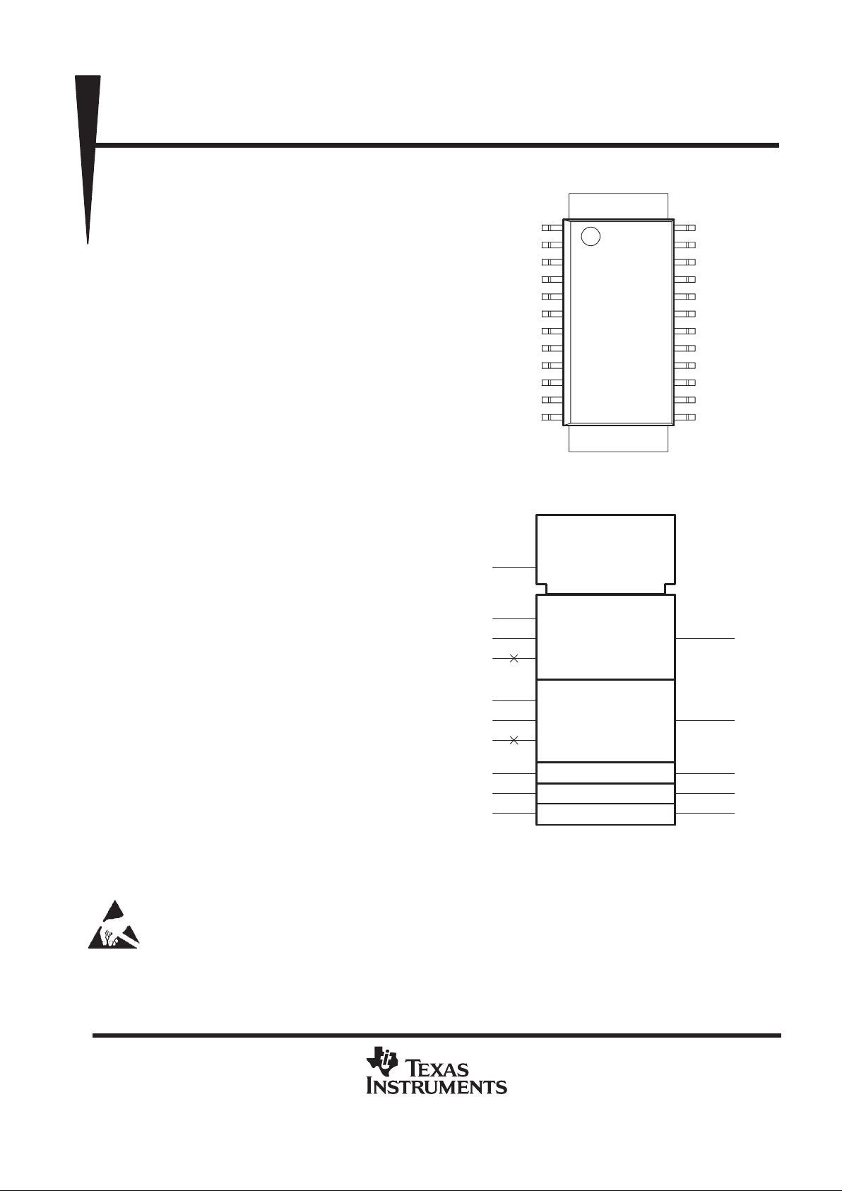
The TMC57253 is available in a 24-pin HSOP-B
surface-mount package and is characterized for
operation from –20°C to 45°C.
This device contains circuits to protect its inputs and outputs against damage due to high static voltages or electrostatic fields. These
circuits have been qualified to protect this device against electrostatic discharges (ESD) of up to 2 kV according to MIL-STD-883C,
Method 3015; however, it is advised that precautions be taken to avoid application of any voltage higher than maximum-rated voltages
to these high-impedance circuits. During storage or handling, the device leads should be shorted together or the device should be
placed in conductive foam. In a circuit, unused inputs should always be connected to an appropriated logic voltage level, preferably either V
CC
or ground. Specific guidelines for handling devices of this type are contained in the publication
Guidelines for Handling
Electrostatic-Discharge-Sensitive (ESDS) Devices and Assemblies
available from Texas Instruments.
HSOP TYPE-B
(TOP VIEW)
1
2
3
4
5
6
7
8
9
10
11
12
24
23
22
21
20
19
18
17
16
15
14
13
V
AB
V
CC
GND
EN
ABIN
ABMIN
IA1IN
IA2IN
SAIN
SRIN
SRMIN
GND
V
ABM
ABOUT
V
ABL
GND
IA1OUT
V
IA
IA2OUT
GND
SAOUT
V
S
SROUT
V
SM
7
8
9
4
5
6
24
10
11
13
ABOUT
23
IA1OU
T
20
IA2OU
T
18
SAOUT
16
SROUT
14
Φ
TTL/CCD
EN
ABIN
ABMIN
V
ABM
SRIN
SRMIN
V
SM
IA1IN
IA2IN
SAIN
logic symbol
PRODUCTION DATA information is current as of publication date.
Products conform to specifications per the terms of Texas Instruments
standard warranty. Production processing does not necessarily include
testing of all parameters.
TI is a trademark of Texas Instruments Incorporated.
TMC57253
DRIVER
SOCS040A – MARCH 1994 – REVISED NOVEMBER 1994
2
POST OFFICE BOX 655303 • DALLAS, TEXAS 75265
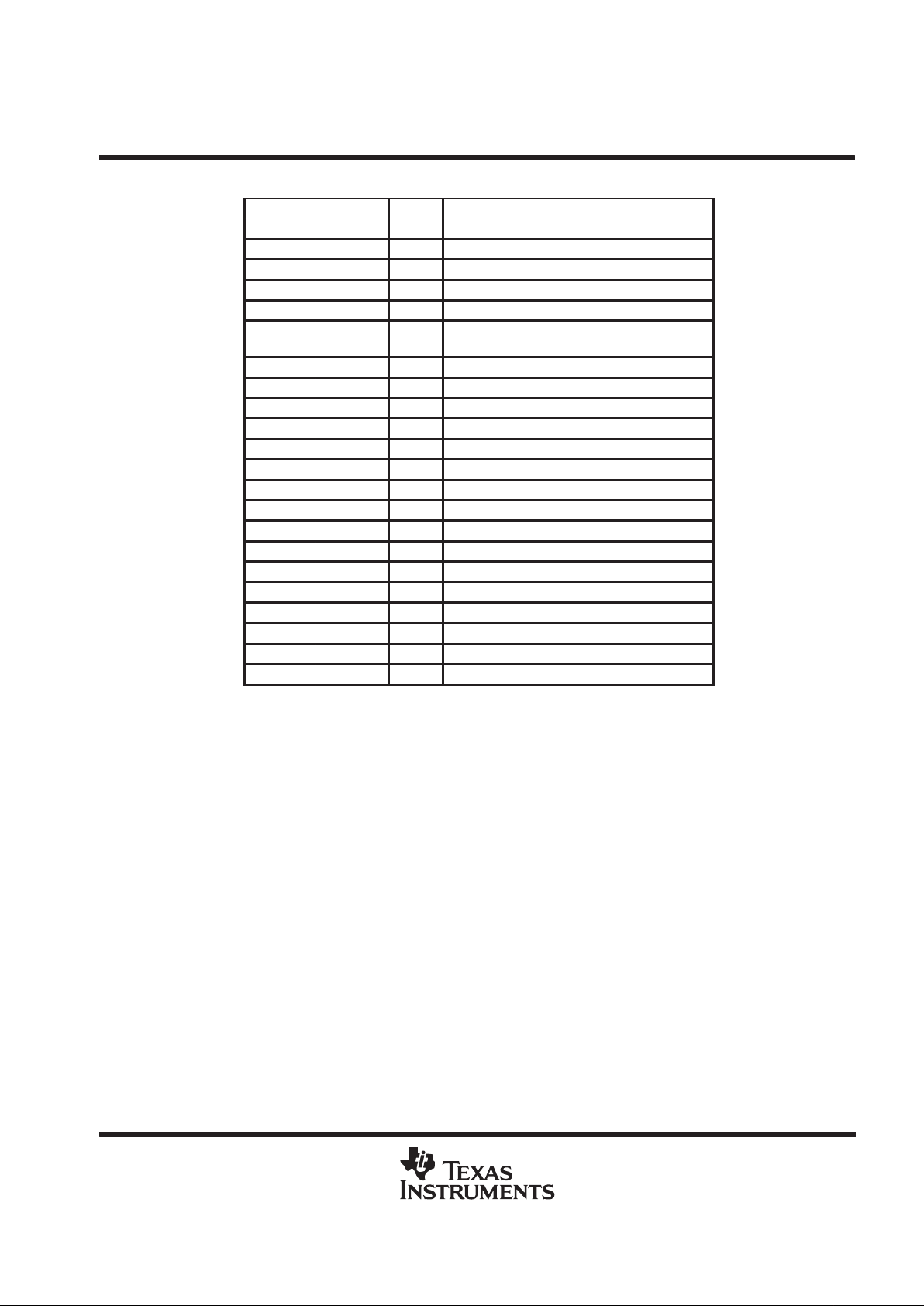
Terminal Functions
TERMINAL
NAME NO.
I/O
DESCRIPTION
ABIN 5 I Antiblooming input
ABMIN 6 I Antiblooming midlevel input
ABOUT 23 O Antiblooming output
EN 4 I Enable control input
GND
3, 12, 17,
21
Ground
IA1IN 7 I Image area 1 input
IA1OUT 20 O Image area 1 output
IA2IN 8 I Image area 2 input
IA2OUT 18 O Image area 2 output
SAIN 9 I Storage area input
SAOUT 16 O Storage area output
SRIN 10 I Serial register input
SRMIN 11 I Serial register mid input
SROUT 14 O Serial register output
V
AB
1 High-level antiblooming supply voltage
V
ABL
22 Low-level antiblooming supply voltage
V
ABM
24 Midlevel antiblooming supply voltage
V
CC
2 Supply voltage
V
IA
19 Image supply voltage
V
S
15 Serial and storage-gate supply voltage
V
SM
13 Midlevel serial-gate supply voltage

TMC57253
DRIVER
SOCS040A – MARCH 1994 – REVISED NOVEMBER 1994
3
POST OFFICE BOX 655303 • DALLAS, TEXAS 75265
functional block diagram
Level
Shift
Level
Shift
Level
Shift
Level
Shift
Level
Shift
Level
Shift
Level
Shift
HV_BUF
and
Driver
HV_BUF
and
Driver
HV_BUF
and
Driver
HV_BUF
and
Driver
HV_BUF
and
Driver
Logic
4
2
1
5
6
7
8
9
10
11
22
23
24
20
19
18
16
15
14
13
V
ABM
ABOUT
V
ABL
IA1OUT
V
IA
IA2OUT
SAOUT
V
S
SROUT
V
SM
V
AB
V
CC
EN
ABIN
ABMIN
IA1IN
IA2IN
SAIN
SRIN
SRMIN
TMC57253
DRIVER
SOCS040A – MARCH 1994 – REVISED NOVEMBER 1994
4
POST OFFICE BOX 655303 • DALLAS, TEXAS 75265
absolute maximum ratings over operating free-air temperature range (unless otherwise noted)
†
Supply voltage range, V
CC
(see Note 1) 0 V to 20 V. . . . . . . . . . . . . . . . . . . . . . . . . . . . . . . . . . . . . . . . . . . . . . . .
Continuous total power dissipation at (or below) T
A
= 25°C:
Unmounted device (see Figure 1) 1990 mW. . . . . . . . . . . . . . . . . . . . . . . . . . . . . . . . . . . . . . . . . . . . . . . . . . . . .
Mounted device (see Figure 1) 2754 mW. . . . . . . . . . . . . . . . . . . . . . . . . . . . . . . . . . . . . . . . . . . . . . . . . . . . . . .
Operating free-air temperature range, T
A
–20°C to 45°C. . . . . . . . . . . . . . . . . . . . . . . . . . . . . . . . . . . . . . . . . . . .
Storage temperature range, T
STG
–55°C to 125°C. . . . . . . . . . . . . . . . . . . . . . . . . . . . . . . . . . . . . . . . . . . . . . . . .
Lead temperature: 1,6 mm (1/16 inch) from case for 10 seconds 260°C. . . . . . . . . . . . . . . . . . . . . . . . . . . . . .
1,6 mm (1/16 inch) from case for 3 seconds 350°C. . . . . . . . . . . . . . . . . . . . . . . . . . . . . . .
†
Stresses beyond those listed under “absolute maximum ratings” may cause permanent damage to the device. These are stress ratings only, and
functional operation of the device at these or any other conditions beyond those indicated under “recommended operating conditions” is not
implied. Exposure to absolute-maximum-rated conditions for extended periods may affect device reliability.
NOTE 1: All voltages are with respect to GND.
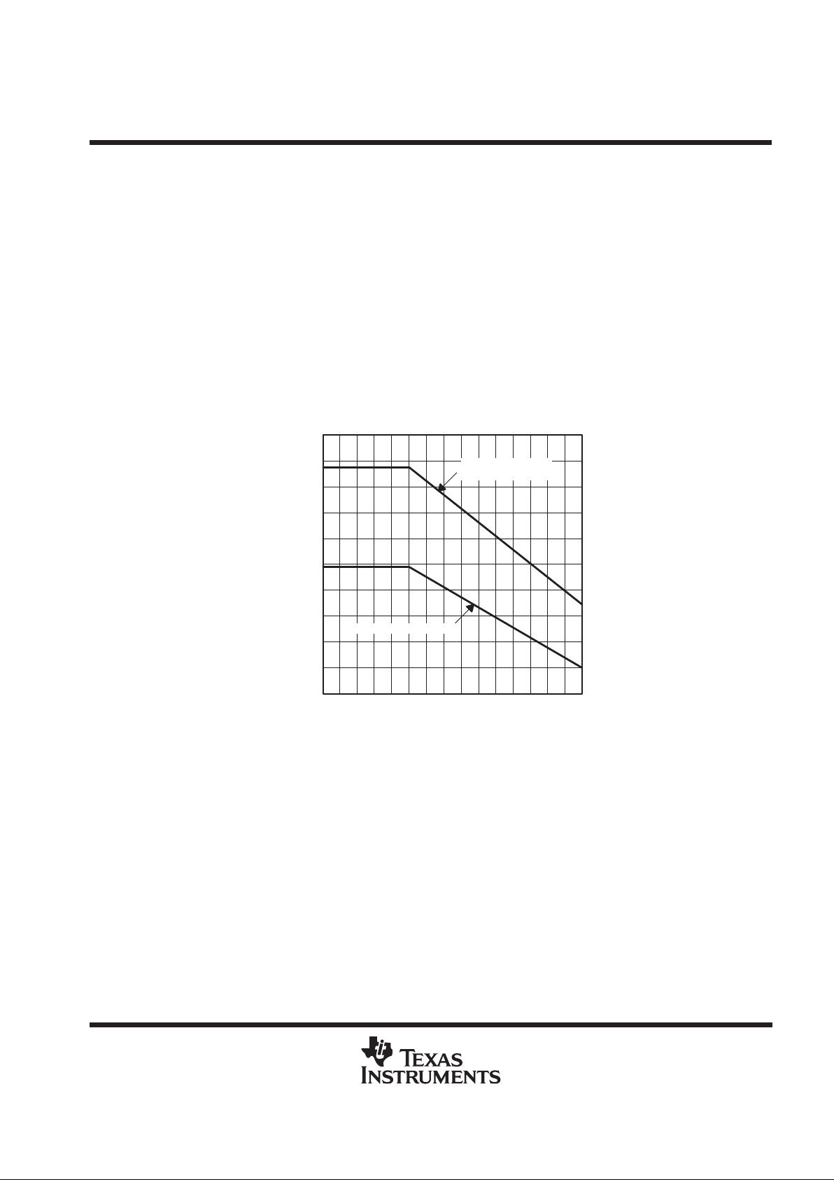
01020304050605 152535455565
3000
2800
2600
2400
2200
2000
1800
1600
1400
1200
1000
TA– Free-Air Temperature–°C
P
D
– Power Dissipation – mW
70 75
Unmounted Device
Mounted Device
(see Note A)
POWER DISSIPATION
vs
FREE-AIR TEMPERATURE
NOTE A: The mounted-device derating curve of Figure 1 is obtained under the following conditions:
The board is 50 mm by 50 mm by 1.6 mm thick.
The board material is glass epoxy.
The copper thickness of all the etch runs is 35 microns.
Etch-run dimensions – All twenty etch runs are 0.4 mm by 22 mm.
Each chip is soldered to the board.
An aluminum cooling fin 10 mm by 10 mm by 1 mm thick is coupled to the chip with thermal paste.
Figure 1

TMC57253
DRIVER
SOCS040A – MARCH 1994 – REVISED NOVEMBER 1994
5
POST OFFICE BOX 655303 • DALLAS, TEXAS 75265
recommended operating conditions
MIN NOM MAX UNIT
Supply voltage, V
CC
4.5 5 5.5 V
Antiblooming supply voltage, V
AB
8 18 V
Low-level antiblooming supply voltage, V
ABL
0 3 V
Midlevel antiblooming supply voltage, V
ABM
3 10 V
Image-gate supply voltage, V
IA
8 14 V
Serial and storage-gate supply voltage, V
S
8 14 V
Serial-gate midlevel supply voltage, V
SM
3 7 V
High-level input voltage, V
IH
2.5 V
Low-level input voltage, V
IL
0.9 V
IA1OUT, IA2OUT (fast clear) 25 MHz
IA1OUT, IA2OUT (transfer) 12.5 MHz
Frequency, f
clock
SAOUT (transfer) 12.5 MHz
ABOUT 12.5 MHz
SROUT 12.5 MHz
IA1OUT, IA2OUT, SAOUT 1%
Drive mode (on ratio)
ABOUT 23%
SROUT 85%
Operating free-air temperature, T
A
–20 45 °C
electrical characteristics over recommended ranges of supply voltage and operating free-air
temperature (unless otherwise noted)
PARAMETER TEST CONDITIONS MIN TYP MAX UNIT
V
OH
High-level output voltage IOH = 0.5 mA 12 V
V
OL
Low-level output voltage IOL = 0 0 V
I
IH
High-level input current VIH = 5 V ±10 µA
I
IL
Low-level input current VIL = 0 ±10 µA
I
CC
Supply current VCC = 5 V 0.1 mA
I
IA
Image-gate supply current VIA = 12 V 5 mA
I
AB
Antiblooming supply current 15 mA
I
ABL
Low-level antiblooming supply current
VAB = 12 V
15 mA
I
ABM
Midlevel antiblooming supply current 0.5 mA
I
SM
Midlevel serial-gate supply current
2 mA
I
S
Serial-gate supply current
V
S
= 12
V
2 mA
IA1OUT,
IA2OUT,
SAOUT
IO = 10 mA,
VI = VCC, GND
VIA = 8 V
5
r
o
Output resistance
ABOUT
IO = 10 mA,
VSM = 4 V,
VI = VCC, GND
VAB = 8 V,
V
ABM
= 4 V
V
ABL
= 0 V
10
Ω
SROUT
IO = 10 mA,
VSM = 4 V,
VS= 8 V,
VI = VCC, GND
50

TMC57253
DRIVER
SOCS040A – MARCH 1994 – REVISED NOVEMBER 1994
6
POST OFFICE BOX 655303 • DALLAS, TEXAS 75265
switching characteristics for ABOUT, IA1OUT, IA2OUT, SAOUT, and SROUT, VAB = 13 V,
V
ABI
= 1.5 V,V
ABM
= 6.5 V, VIA = 11 V, VSM = 5 V, VS = 11 V, TA = 25°C (unless otherwise noted)
†
PARAMETER
FROM
(INPUT)
TO
(OUTPUT)
TEST CONDITIONS MIN MAX UNIT
IA1IN IA1OUT
IA2IN IA2OUT
See Figure 3 85
SAIN SAOUT
t
pd
Propagation delay time
SRIN
ns
SRMIN
SROUT
See Figure 4
40
80
ABIN
ABMIN
ABOUT
See Figure 5
90
IA1OUT
IA2OUT
t
PLZ
Disable time EN
SAOUT
See Figure 6 1ns
SROUT
ABOUT
IA1OUT
IA2OUT
t
PZH
Enable time EN
SAOUT
See Figure 6 1ns
SROUT
ABOUT
IA1OUT
IA2OUT
See Figure 3, tc = 80 ns 40% 60%
Duty cycle
‡
SAOUT
ABOUT See Figure 3, tc = 160 ns 40% 60%
†
The load is a Texas Instruments TC255 CCD image sensor.
‡
Duty cycle
+
t
w
H
(t
w
H
)
t
w
L
)
100

TMC57253
DRIVER
SOCS040A – MARCH 1994 – REVISED NOVEMBER 1994
7
POST OFFICE BOX 655303 • DALLAS, TEXAS 75265
PARAMETER MEASUREMENT INFORMATION
5 ns MAX
t
f
V
IH
V
IL
90%
10%
5 ns MAX
t
r
Figure 2. Rise and Fall Time Requirements for Input Signals
50%
t
PLH
t
PHL
50%
t
wL
t
wH
GND
GND
V
CC
VIA or V
S
IA1IN, IA2IN, SAIN
IA1OUT, IA2OUT, SAOUT
NOTE A: tpd = t
PLH
or t
PHL
Figure 3. Duty Cycle and Propagation Delay
26 ns
MIN
54 ns MIN
50%
SRIN
SRMIN
SROUT
50%
t
PHL
t
PLH
t
PHL
5 ns MAX
†
26 ns MIN
†
V
CC
GND
V
S
GND
V
S
V
SM
GND
50% V
S
50% V
SM
†
If SRIN and SRMIN are both high, SROUT follows SRIN.
NOTE A: tpd = t
PLH
or t
PHL
Figure 4. Serial-Register-Driver Waveforms

TMC57253
DRIVER
SOCS040A – MARCH 1994 – REVISED NOVEMBER 1994
8
POST OFFICE BOX 655303 • DALLAS, TEXAS 75265
PARAMETER MEASUREMENT INFORMATION
80 ns MIN80 ns MIN
166 ns MIN
50%
t
PHL
t
PLH
50% 50%
t
PLH
t
PHL
50% V
ABM
50%
V
CC
GND
V
CC
GND
V
AB
V
ABL
ABIN
ABMIN
ABOUT
V
ABM
NOTES: A. VAB and V
ABM
are in a short-circuit condition if ABIN and ABMIN are held high at the same time. This short-circuit condition can
destroy the device.
B. tpd = t
PLH
or t
PHL
Figure 5. Antiblooming-Driver Waveforms
VAB or V
ABM
t
PLZ
t
PZH
t
PLZ
t
PZH
GND
VIM or V
S
50%
GND
GND
V
CC
ABOUT
IA1OUT, IA2OUT,
SAOUT, SROUT
EN
50% 50%
50%
50% 50%
Figure 6. Enable Waveforms

TMC57253
DRIVER
SOCS040A – MARCH 1994 – REVISED NOVEMBER 1994
9
POST OFFICE BOX 655303 • DALLAS, TEXAS 75265
MECHANICAL DATA
HSOP-B plastic small-outline package
This small-outline package consists of a circuit mounted on a lead frame and encapsulated within a plastic compound.
The compound will withstand soldering temperature with no deformation, and circuit performance characteristics will
remain stable when operated in high-humidity conditions. Leads require no additional cleaning or processing when
used in soldered assembly.
Seating Plane
0,15
M
0,13
1,27
24 13
112
0,50
0,30
0,20
0,30
15,20
15,40
2,65 MAX
0,10 MIN
10,80
10,00
7,40
7,60
1,20
0,40
6,65
6,35
19,50
18,90
0°–10°
7/94
NOTES: A. All linear dimensions are in millimeters.
B. This drawing is subject to change without notice.
C. Body dimensions do not include mold flash or protrusion.

TMC57253
DRIVER
SOCS040A – MARCH 1994 – REVISED NOVEMBER 1994
10
POST OFFICE BOX 655303 • DALLAS, TEXAS 75265
MECHANICAL DATA
15,3
0,76
0,51
1,7
7,8 10,8
1,27
112
1324
ALL LINEAR DIMENSIONS ARE IN MILLIMETERS
7,0
Figure 7. 24-Pin/375-mil HSOP Land Design

IMPORTANT NOTICE
T exas Instruments and its subsidiaries (TI) reserve the right to make changes to their products or to discontinue
any product or service without notice, and advise customers to obtain the latest version of relevant information
to verify, before placing orders, that information being relied on is current and complete. All products are sold
subject to the terms and conditions of sale supplied at the time of order acknowledgement, including those
pertaining to warranty, patent infringement, and limitation of liability.
TI warrants performance of its semiconductor products to the specifications applicable at the time of sale in
accordance with TI’s standard warranty. Testing and other quality control techniques are utilized to the extent
TI deems necessary to support this warranty. Specific testing of all parameters of each device is not necessarily
performed, except those mandated by government requirements.
CERT AIN APPLICATIONS USING SEMICONDUCTOR PRODUCTS MAY INVOLVE POTENTIAL RISKS OF
DEATH, PERSONAL INJURY, OR SEVERE PROPERTY OR ENVIRONMENTAL DAMAGE (“CRITICAL
APPLICATIONS”). TI SEMICONDUCTOR PRODUCTS ARE NOT DESIGNED, AUTHORIZED, OR
WARRANTED TO BE SUITABLE FOR USE IN LIFE-SUPPORT DEVICES OR SYSTEMS OR OTHER
CRITICAL APPLICATIONS. INCLUSION OF TI PRODUCTS IN SUCH APPLICA TIONS IS UNDERST OOD TO
BE FULLY AT THE CUSTOMER’S RISK.
In order to minimize risks associated with the customer’s applications, adequate design and operating
safeguards must be provided by the customer to minimize inherent or procedural hazards.
TI assumes no liability for applications assistance or customer product design. TI does not warrant or represent
that any license, either express or implied, is granted under any patent right, copyright, mask work right, or other
intellectual property right of TI covering or relating to any combination, machine, or process in which such
semiconductor products or services might be or are used. TI’s publication of information regarding any third
party’s products or services does not constitute TI’s approval, warranty or endorsement thereof.
Copyright 1998, Texas Instruments Incorporated
 Loading...