


M i l i t a r y S e m i c o n d u c t o r P r o d u c t s
Fact Sheet
Fact Sheet
TLV5618AM / 5962-9955701QxA
SGYV073, October 1999
TLV5618AM, 2.7-V TO 5.5-V LOW POWER DUAL 12-BIT DC WITH POWER DOWN
HIGHLIGHTS
The TLV5618AM is a dual 12-bit voltage output DAC with a flexible 3-wire serial interface. The serial
interface is compatible with SMJ320 DSPs, SPITM, QSPITM, and MicrowireTM serial ports. It is
programmed with a 16-bit serial string containing 4 control and 12 data bits.
The resistor string output voltage is buffered by an x2 gain rail-to-rail output buffer. The buffer features
a Class-AB output stage to improve stability and reduce settling time. The programmable settling
time of the DAC allows the designer to optimize speed versus power dissipation.
Implemented with a CMOS process, the device is designed for single supply operation from 2.7 V to
5.5 V. The TLV5618AM is characterized for operation from -55°C to 125°C.
KEY FEATURES/BENEFITS
• Programmable Settling Time to 0.5 LSB
2.5 us or 12.5 us Typ
• Simultaneous Updates for DAC A and DAC B
• Single Supply Operation
• 3-Wire Serial Interface
• Output Voltage Range ... 2 Times the Reference Input Voltage
• Software Powerdown Mode
• Internal Power-On Reset
• SMJ320 DSP and SPITM Compatible
• Low Power Consumption:
3 mW Typ in Slow Mode,
8 mW Typ in Fast Mode
• Input Data Update Rate of 1.21 MHz
DIE SIZE
The current die (BDLE5618AIN) has a size of: 60 x 68 mils
TECHNOLOGY
• 0.8-µm LinEPIC-1ZS CMOS Process
• Class 2 ESD rating per MIL-STD-883, Method 30
Trademarks are the property of their respective owners.
PACKAGING
Package Option: 8-pin Ceramic Dual in Line Package (JG )
20-pin Leadless Ceramic Chip Carrier (FK)
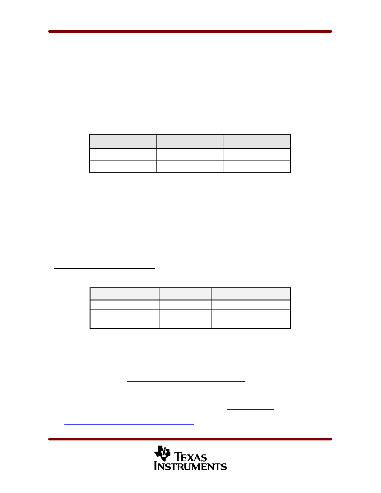
POWER DISSIPATION
The table below shows modeled data. This data can be used for approximating system thermal
characteristics:
Package Thermal Data
Package
8-Pin DIP 119º C/W 15º C/W
20-Pin LCC 91º C/W 6º C/W
Note: much better thermal impedances can be achieved by using air flow, or by increasing metal
backplane thickness or trace area in the Printed Circuit Board (PCB) that is used.
RθJA RθJC
PROCESS/PERFORMANCE OPTIONS
The TLV5618AM is processed to the military temperature range at the SN-level, or at the SNJ-level for
programs requiring devices processed to MIL-PRF-38535. The DSCC Standard Microcircuit Drawings
(SMD) for these device are given below.
MILITARY TLV5618AM FAMILY:
The following table details the military TLV5618AM products currently offered by TI:
Device # Of Pins DSCC Number
TLV5618AMJGB 8
TLV5618AMFKB 20 5962-9955701Q2A
TLV5618AMJG 8 -----------
5962-9955701QPA
SUPPORT
Additional information regarding this product is available by calling the Texas Instruments Product
Information Center (PIC) at (972) 644-5580 during normal business hours (CST/CDT) . Online
information is available at : http://www.ti.com/sc/docs/pic/americas.htm
SUPPORT LITERATURE
You can access data sheets via TI’s home page on the internet (http://www.ti.com) or reference the
literature number SLAS230b when contacting the PIC. Our military products internet site is available
at: http://www.ti.com/sc/docs/military/welcome.htm
 Loading...