

Texas Instruments TLV2217-33PWLE, TLV2217-33PWR, TLV2217-33MJB, TLV2217-33MFKB, TLV2217-33KTPR Datasheet
TLV2217-33
LOW-DROPOUT 3.3-V FIXED-VOLTAGE REGULATORS
SLVS067G – MARCH 1992 – REVISED JULY 1999
1
POST OFFICE BOX 655303 • DALLAS, TEXAS 75265
D
Fixed 3.3-V Output
D
±1% Maximum Output Voltage Tolerance at
TJ = 25°C
D
500-mV Maximum Dropout V oltage at
500 mA
D
500-mA Dropout Current
D
±2% Absolute Output Voltage Variation
D
Internal Overcurrent Limiting
D
Internal Thermal-Overload Protection
D
Internal Overvoltage Protection
D
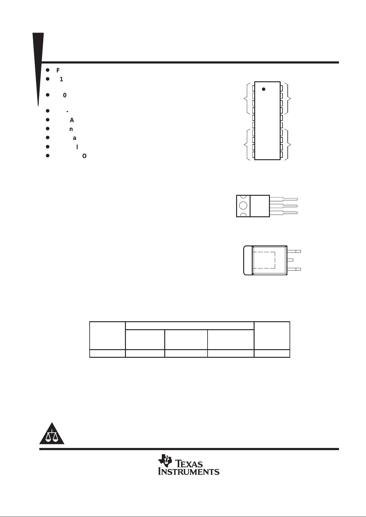
Package Options Include Plastic Flange
Mounted (KTP), Power (KC), and Thin
Shrink Small-Outline (PW) Packages
description
The TLV2217-33 is a low-dropout 3.3-V fixedvoltage regulator. The regulator is capable of
sourcing 500 mA of current with an input-output
differential of 0.5 V, or less. The TLV2217-33
provides internal overcurrent limiting, thermaloverload protection, and overvoltage protection.
The 0.5-V dropout for the TLV2217-33 makes it
ideal for battery applications in 3.3-V logic
systems. For example, battery input voltage to the
regulator can drop as low as 3.8 V, and the
TL V2217-33 can continue to regulate the system.
For higher voltage systems, the TL V2217-33 can
be operated with a continuous input voltage of
12 V.
The TLV2217-33 regulators are characterized for virtual junction temperature operation from 0°C to 125°C .
AVAILABLE OPTIONS
PACKAGED DEVICES
T
J
PLASTIC
POWER
(KC)
SURFACE
MOUNT
(PW)
PLASTIC
FLANGE MOUNT
(KTP)
CHIP FORM
(Y)
0°C to 125°C TLV2217-33KC TLV2217-33PW TLV2217-33KTP TLV2217-33Y
The KTP and PW packages are available taped and reeled only. Add R suffix to device type
(e.g., TLV2212-33PWR). Chip forms are tested at 25°C.
Please be aware that an important notice concerning availability, standard warranty, and use in critical applications of
Texas Instruments semiconductor products and disclaimers thereto appears at the end of this data sheet.
Copyright 1999, Texas Instruments Incorporated
PRODUCTION DATA information is current as of publication date.
Products conform to specifications per the terms of Texas Instruments
standard warranty. Production processing does not necessarily include
testing of all parameters.
OUTPUT
GND
INPUT
1
2
3
4
5
6
7
8
9
10
20
19
18
17
16
15
14
13
12
11
GND
INPUT
GND
OUTPUT
PW PACKAGE
(TOP VIEW)
HEAT
SINK
HEAT
SINK
HEAT
SINK
HEAT
SINK
KC PACKAGE
(TOP VIEW)
HEAT SINK – These terminals have an internal resistive connection
to ground and should be grounded or electrically isolated.
OUTPUT
GND
INPUT
GND
KTP PACKAGE
(TOP VIEW)
The GND terminal is in electrical contact with the mounting base.
The GND terminal is in electrical contact with the mounting base.
GND
TLV2217-33
LOW-DROPOUT 3.3-V FIXED-VOLTAGE REGULATORS
SLVS067G – MARCH 1992 – REVISED JULY 1999
2
POST OFFICE BOX 655303 • DALLAS, TEXAS 75265
absolute maximum ratings over operating virtual junction temperature range (unless otherwise
noted)
†
Continuous input voltage, VI 16 V. . . . . . . . . . . . . . . . . . . . . . . . . . . . . . . . . . . . . . . . . . . . . . . . . . . . . . . . . . . . . . . . .
Package thermal impedance, θJA (see Notes 1 and 2): KC package 22°C/W. . . . . . . . . . . . . . . . . . . . . . . . . . .
KTP package 28°C/W. . . . . . . . . . . . . . . . . . . . . . . . .
PW package 83°C/W. . . . . . . . . . . . . . . . . . . . . . . . . .
Storage temperature range, T
stg
–65°C to 150°C. . . . . . . . . . . . . . . . . . . . . . . . . . . . . . . . . . . . . . . . . . . . . . . . . . .
†
Stresses beyond those listed under “absolute maximum ratings” may cause permanent damage to the device. These are stress ratings only, and
functional operation of the device at these or any other conditions beyond those indicated under “recommended operating conditions” is not
implied. Exposure to absolute-maximum-rated conditions for extended periods may affect device reliability.
NOTES: 1. Maximum power dissipation is a function of TJ(max),
θ
JA
, and TA. The maximum allowable power dissipation at any allowable
ambient temperature is PD = (TJ(max) – TA)/
θ
JA
. Operating at the absolute maximum TJ of 150°C can impact reliability. Due to
variation in individual device electrical characteristics and thermal resistance, the built-in thermal overload protection may be
activated at power levels slightly above or below the rated dissipation.
2. The package thermal impedance is calculated in accordance with JESD 51, except for through-hole packages, which use a trace
length of zero.
recommended operating conditions
MIN MAX UNIT
Input voltage, V
I
3.8 12 V
Output current, I
O
0 500 mA
Operating virtual junction temperature range, T
J
0 125 °C
electrical characteristics at V
I
= 4.5 V, IO = 500 mA, T
J
= 25°C (unless otherwise noted)
TLV2217-33 UNIT
PARAMETER
TEST CONDITIONS
‡
MIN TYP MAX UNIT
p
TJ = 25°C 3.267 3.30 3.333
Output voltage
I
O
= 20 mA to
500 mA
,
V
I
= 3.8 V to 5.5
V
TJ = 0°C to 125°C 3.234 3.366
V
Input voltage regulation VI = 3.8 V to 5.5 V 5 15 mV
Ripple rejection f = 120 Hz, V
ripple
= 1 V
PP
–62 dB
Output voltage regulation IO = 20 mA to 500 mA 5 30 mV
Output noise voltage f = 10 Hz to 100 kHz 500 µV
p
IO = 250 mA 400
Dropout voltage
IO = 500 mA 500
mV
IO = 0 2 5
Bias current
IO = 500 mA 19 49
mA
‡
Pulse-testing techniques are used to maintain the virtual junction temperature as close to the ambient temperature as possible. Thermal effects
must be taken into account separately. All characteristics are measured with a 0.1-µF capacitor across the input and a 22-µF tantalum capacitor
with equivalent series resistance of 1.5 Ω on the output.

TLV2217-33
LOW-DROPOUT 3.3-V FIXED-VOLTAGE REGULATORS
SLVS067G – MARCH 1992 – REVISED JULY 1999
3
POST OFFICE BOX 655303 • DALLAS, TEXAS 75265
electrical characteristics at V
I
= 4.5 V, I
O
= 500 mA, TJ = 25°C (unless otherwise noted)
TLV2217-33Y
PARAMETER
TEST CONDITIONS
†
MIN TYP MAX
UNIT
Output voltage IO = 20 mA to 500 mA, VI = 3.8 V to 5.5 V 3.267 3.30 3.333 V
Input voltage regulation VI = 3.8 V to 5.5 V 5 15 mV
Ripple rejection f = 120 Hz, V
ripple
= 1 V
PP
–62 dB
Output voltage regulation IO = 20 mA to 500 mA 5 30 mV
Output noise voltage f = 10 Hz to 100 kHz 500 µV
p
IO = 250 mA 400
Dropout voltage
IO = 500 mA 500
mV
IO = 0 2 5
Bias current
IO = 500 mA 19 49
mA
†
Pulse-testing techniques are used to maintain the virtual junction temperature as close to the ambient temperature as possible. Thermal effects
must be taken into account separately. All characteristics are measured with a 0.1-µF capacitor across the input and a 22-µF tantalum capacitor
with equivalent series resistance of 1.5 Ω on the output.
TLV2217-33
LOW-DROPOUT 3.3-V FIXED-VOLTAGE REGULATORS
SLVS067G – MARCH 1992 – REVISED JULY 1999
4
POST OFFICE BOX 655303 • DALLAS, TEXAS 75265
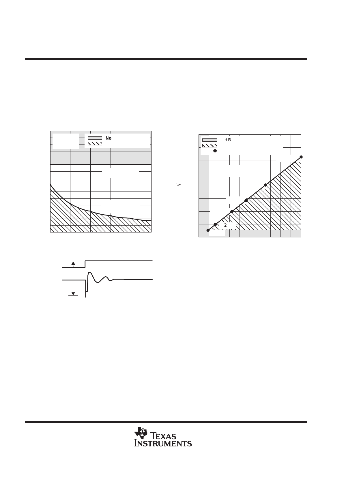
COMPENSATION-CAPACITOR SELECTION INFORMATION
The TLV2217-33 is a low-dropout regulator . This means that the capacitance loading is important to the performance
of the regulator because it is a vital part of the control loop. The capacitor value and the equivalent series resistance
(ESR) both affect the control loop and must be defined for the load range and the temperature range. Figures 1 and 2
can be used to establish the capacitance value and ESR range for best regulator performance.
ESR OF OUTPUT CAPACITOR
vs
LOAD CURRENT
Figure 1
ESR – Equivalent Series Resistance –
1
0.8
0.4
0.2
0
1.8
0.6
0 0.1 0.2 0.3
1.4
1.2
1.6
3
0.4 0.5
2
2.2
2.4
2.6
2.8
Ω
∆I
L
∆V
L
∆VL = ESR × ∆I
L
Not Recommended
Potential Instability
CL = 22 µF
CI = 0.1 µF
TJ = 25°C
Maximum
ESR Boundary
Applied Load
Current
Load
Voltage
IL – Load Current – A
Minimum
ESR Boundary
10 µF
STABILITY
vs
ESR
Figure 2
C
L
0.015
0.01
0
0 0.5 1 1.5 2 3 4
0.025
0.035
1/ESR
0.04
4.5 5
0.005
0.03
0.02
22 µF
1000 µF
2.5 3.5
100 mF
200 µF
400 µF
Not Recommended
Potential Instability
Recommended Minimum ESR
Region of
Best Stability

TLV2217-33
LOW-DROPOUT 3.3-V FIXED-VOLTAGE REGULATORS
SLVS067G – MARCH 1992 – REVISED JULY 1999
5
POST OFFICE BOX 655303 • DALLAS, TEXAS 75265
APPLICATION INFORMATION
application schematic
VO = 3.3 V
22 µF
3.8 V
0.1 µF
TLV2217-33
INPUT OUTPUT
Figure 3

IMPORTANT NOTICE
T exas Instruments and its subsidiaries (TI) reserve the right to make changes to their products or to discontinue
any product or service without notice, and advise customers to obtain the latest version of relevant information
to verify, before placing orders, that information being relied on is current and complete. All products are sold
subject to the terms and conditions of sale supplied at the time of order acknowledgement, including those
pertaining to warranty, patent infringement, and limitation of liability.
TI warrants performance of its semiconductor products to the specifications applicable at the time of sale in
accordance with TI’s standard warranty. Testing and other quality control techniques are utilized to the extent
TI deems necessary to support this warranty. Specific testing of all parameters of each device is not necessarily
performed, except those mandated by government requirements.
CERT AIN APPLICATIONS USING SEMICONDUCTOR PRODUCTS MAY INVOLVE POTENTIAL RISKS OF
DEATH, PERSONAL INJURY, OR SEVERE PROPERTY OR ENVIRONMENTAL DAMAGE (“CRITICAL
APPLICATIONS”). TI SEMICONDUCTOR PRODUCTS ARE NOT DESIGNED, AUTHORIZED, OR
WARRANTED TO BE SUITABLE FOR USE IN LIFE-SUPPORT DEVICES OR SYSTEMS OR OTHER
CRITICAL APPLICATIONS. INCLUSION OF TI PRODUCTS IN SUCH APPLICA TIONS IS UNDERSTOOD T O
BE FULLY AT THE CUSTOMER’S RISK.
In order to minimize risks associated with the customer’s applications, adequate design and operating
safeguards must be provided by the customer to minimize inherent or procedural hazards.
TI assumes no liability for applications assistance or customer product design. TI does not warrant or represent
that any license, either express or implied, is granted under any patent right, copyright, mask work right, or other
intellectual property right of TI covering or relating to any combination, machine, or process in which such
semiconductor products or services might be or are used. TI’s publication of information regarding any third
party’s products or services does not constitute TI’s approval, warranty or endorsement thereof.
Copyright 1999, Texas Instruments Incorporated
 Loading...