

TLC5615C, TLC5615I
10-BIT DIGITAL-TO-ANALOG CONVERTERS
SLAS142C – OCTOBER 1996 – REVISED MARCH 2000
D
10-Bit CMOS Voltage Output DAC in an
8-T erminal Package
D
5-V Single Supply Operation
D
3-Wire Serial Interface
D
High-Impedance Reference Inputs
D
Voltage Output Range ...2 Times the
Reference Input Voltage
D
Internal Power-On Reset
D
Low Power Consumption . . . 1.75 mW Max
D
Update Rate of 1.21 MHz
D
Settling Time to 0.5 LSB . . . 12.5 µs Typ
D
Monotonic Over Temperature
D
Pin Compatible With the Maxim MAX515
description
The TLC5615 is a 10-bit voltage output digital-to-analog converter (DAC) with a buffered reference input (high
impedance). The DAC has an output voltage range that is two times the reference voltage, and the DAC is
monotonic. The device is simple to use, running from a single supply of 5 V. A power-on-reset function is
incorporated to ensure repeatable start-up conditions.
applications
D
Battery-Powered T est Instruments
D
Digital Offset and Gain Adjustment
D
Battery Operated/Remote Industrial
Controls
D
Machine and Motion Control Devices
D
Cellular Telephones
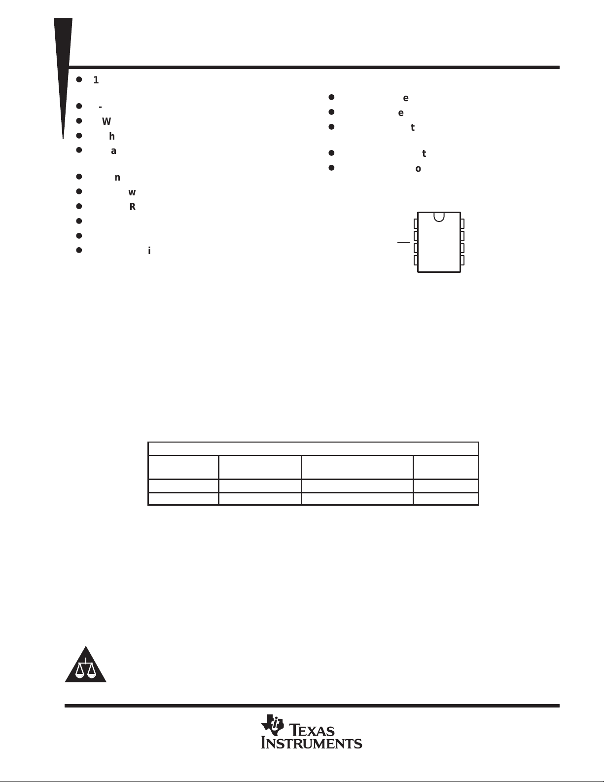
D, P, OR DGK PACKAGE
(TOP VIEW)
DIN
SCLK
CS
DOUT
1
2
3
4
8
7
6
5
V
DD
OUT
REFIN
AGND
Digital control of the TLC5615 is over a three-wire serial bus that is CMOS compatible and easily interfaced to
industry standard microprocessor and microcontroller devices. The device receives a 16-bit data word to
produce the analog output. The digital inputs feature Schmitt triggers for high noise immunity. Digital
communication protocols include the SPI, QSPI, and Microwire standards.
The 8-terminal small-outline D package allows digital control of analog functions in space-critical applications.
The TLC5615C is characterized for operation from 0°C to 70°C. The TLC5615I is characterized for operation
from –40°C to 85°C.
AVAILABLE OPTIONS
PACKAGE
T
A
0°C to 70°C TLC5615CD TLC5615CDGK TLC5615CP
–40°C to 85°C TLC5615ID TLC5615IDGK TLC5615IP
†
Available in tape and reel as the TLC5615CDR and the TLC5615IDR
SMALL OUTLINE
(D)
†
PLASTIC SMALL OUTLINE
(DGK)
PLASTIC DIP
(P)
Please be aware that an important notice concerning availability, standard warranty, and use in critical applications of
Texas Instruments semiconductor products and disclaimers thereto appears at the end of this data sheet.
SPI and QSPI are trademarks of Motorola, Inc.
Microwire is a trademark of National Semiconductor Corporation.
PRODUCTION DATA information is current as of publication date.
Products conform to specifications per the terms of Texas Instruments
standard warranty. Production processing does not necessarily include
testing of all parameters.
POST OFFICE BOX 655303 • DALLAS, TEXAS 75265
Copyright 2000, Texas Instruments Incorporated
1
TLC5615C, TLC5615I
I/O
DESCRIPTION
10-BIT DIGITAL-TO-ANALOG CONVERTERS
SLAS142C – OCTOBER 1996 – REVISED MARCH 2000
functional block diagram
_
REFIN
AGND
CS
SCLK
DIN
+
Power-ON
Reset
Control
Logic
DAC
RR
10-Bit DAC Register
2
(LSB) (MSB)
0s
10 Data Bits
16-Bit Shift Register
+
_
2
Dummy
OUT
(Voltage Output)
4
Bits
DOUT
Terminal Functions
TERMINAL
NAME NO.
DIN 1 I Serial data input
SCLK 2 I Serial clock input
CS 3 I Chip select, active low
DOUT 4 O Serial data output for daisy chaining
AGND 5 Analog ground
REFIN 6 I Reference input
OUT 7 O DAC analog voltage output
V
DD
8 Positive power supply
absolute maximum ratings over operating free-air temperature range (unless otherwise noted)
Supply voltage (VDD to AGND) 7 V. . . . . . . . . . . . . . . . . . . . . . . . . . . . . . . . . . . . . . . . . . . . . . . . . . . . . . . . . . . . . . .
Digital input voltage range to AGND – 0.3 V to VDD + 0.3 V. . . . . . . . . . . . . . . . . . . . . . . . . . . . . . . . . . . . . . . . . .
Reference input voltage range to AGND – 0.3 V to VDD + 0.3 V. . . . . . . . . . . . . . . . . . . . . . . . . . . . . . . . . . . . . .
Output voltage at OUT from external source V
Continuous current at any terminal ±20 mA. . . . . . . . . . . . . . . . . . . . . . . . . . . . . . . . . . . . . . . . . . . . . . . . . . . . . . . .
Operating free-air temperature range, T
: TLC5615C 0°C to 70°C. . . . . . . . . . . . . . . . . . . . . . . . . . . . . . . . . . . .
A
TLC5615I –40°C to 85°C. . . . . . . . . . . . . . . . . . . . . . . . . . . . . . . . . . .
Storage temperature range, T
–65°C to 150°C. . . . . . . . . . . . . . . . . . . . . . . . . . . . . . . . . . . . . . . . . . . . . . . . . . .
stg
Lead temperature 1,6 mm (1/16 inch) from case for 10 seconds 260°C. . . . . . . . . . . . . . . . . . . . . . . . . . . . . . .
†
Stresses beyond those listed under “absolute maximum ratings” may cause permanent damage to the device. These are stress ratings only, and
functional operation of the device at these or any other conditions beyond those indicated under “recommended operating conditions” is not
implied. Exposure to absolute-maximum-rated conditions for extended periods may affect device reliability.
DD
+ 0.3 V. . . . . . . . . . . . . . . . . . . . . . . . . . . . . . . . . . . . . . . . . . . .
†
2
POST OFFICE BOX 655303 • DALLAS, TEXAS 75265
Operating free-air temperature, T
PSRR
Power-supply rejection ratio
See Notes 7 and 8
dB
TLC5615C, TLC5615I
10-BIT DIGITAL-TO-ANALOG CONVERTERS
SLAS142C – OCTOBER 1996 – REVISED MARCH 2000
recommended operating conditions
MIN NOM MAX UNIT
Supply voltage, V
High-level digital input voltage, V
Low-level digital input voltage, V
Reference voltage, V
Load resistance, R
p
DD
IH
IL
to REFIN terminal 2 2.048 VDD–2 V
ref
L
p
A
TLC5615C 0 70 °C
TLC5615I –40 85 °C
electrical characteristics over recommended operating free-air temperature range, VDD = 5 V ±5%,
= 2.048 V (unless otherwise noted)
V
ref
static DAC specifications
PARAMETER TEST CONDITIONS MIN TYP MAX UNIT
Resolution 10 bits
Integral nonlinearity, end point adjusted (INL) V
Differential nonlinearity (DNL) V
E
E
NOTES: 1. The relative accuracy or integral nonlinearity (INL), sometimes referred to as linearity error, is the maximum deviation of the output
Zero-scale error (offset error at zero scale) V
ZS
Zero-scale-error temperature coefficient V
Gain error V
G
Gain-error temperature coefficient V
pp
Analog full scale output RL = 100 kΩ 2V
from the line between zero and full scale excluding the effects of zero code and full-scale errors (see text).
2. The differential nonlinearity (DNL), sometimes referred to as differential error, is the difference between the measured and ideal 1
LSB amplitude change of any two adjacent codes. Monotonic means the output voltage changes in the same direction (or remains
constant) as a change in the digital input code.
3. Zero-scale error is the deviation from zero-voltage output when the digital input code is zero (see text).
4. Zero-scale-error temperature coefficient is given by: EZSTC = [EZS(T
5. Gain error is the deviation from the ideal output (V
error.
6. Gain temperature coefficient is given by: EGTC = [EG(T
7. Zero-scale-error rejection ratio (EZS-RR) is measured by varying the VDD from 4.5 V to 5.5 V dc and measuring the proportion of
this signal imposed on the zero-code output voltage.
8. Gain-error rejection ratio (EG-RR) is measured by varying the VDD from 4.5 V to 5.5 V dc and measuring the proportion of this signal
imposed on the full-scale output voltage after subtracting the zero-scale change.
Zero scale
Gain
= 2.048 V, See Note 1 ±1 LSB
ref
= 2.048 V, See Note 2 ±0.1 ±0.5 LSB
ref
= 2.048 V, See Note 3 ±3 LSB
ref
= 2.048 V, See Note 4 3 ppm/°C
ref
= 2.048 V, See Note 5 ±3 LSB
ref
= 2.048 V, See Note 6 1 ppm/°C
ref
80
80
) – EZS(T
– 1 LSB) with an output load of 10 kΩ excluding the effects of the zero-scale
ref
) – EG (T
max
max
min
)]/V
× 106/(T
ref
min
4.5 5 5.5 V
2.4 V
2 kΩ
(1023/1024) V
ref
)]/V
max
× 106/(T
ref
– T
min
– T
max
).
0.8 V
).
min
voltage output (OUT)
V
O
I
OSC
V
OL(low)
V
OH(high)
PARAMETER TEST CONDITIONS MIN TYP MAX UNIT
Voltage output range RL = 10 kΩ 0 VDD–0.4 V
Output load regulation accuracy V
Output short circuit current OUT to VDD or AGND 20 mA
Output voltage, low-level I
Output voltage, high-level I
POST OFFICE BOX 655303 • DALLAS, TEXAS 75265
O(OUT)
O(OUT)
= 2 V, RL = 2 kΩ 0.5 LSB
O(OUT)
≤ 5 mA 0.25 V
≤ –5 mA 4.75 V
3
TLC5615C, TLC5615I
IDDPower supply current
10-BIT DIGITAL-TO-ANALOG CONVERTERS
SLAS142C – OCTOBER 1996 – REVISED MARCH 2000
electrical characteristics over recommended operating free-air temperature range, VDD = 5 V ±5%,
V
= 2.048 V (unless otherwise noted) (continued)
ref
reference input (REFIN)
PARAMETER TEST CONDITIONS MIN TYP MAX UNIT
V
Input voltage 0 VDD–2 V
I
r
Input resistance 10 MΩ
i
C
Input capacitance 5 pF
i
digital inputs (DIN, SCLK, CS)
PARAMETER TEST CONDITIONS MIN TYP MAX UNIT
V
High-level digital input voltage 2.4 V
IH
V
Low-level digital input voltage 0.8 V
IL
I
High-level digital input current VI = V
IH
I
Low-level digital input current VI = 0 ±1 µA
IL
C
Input capacitance 8 pF
i
digital output (DOUT)
PARAMETER TEST CONDITIONS MIN TYP MAX UNIT
V
Output voltage, high-level IO = –2 mA VDD–1 V
OH
V
Output voltage, low-level IO = 2 mA 0.4 V
OL
DD
±1 µA
power supply
PARAMETER TEST CONDITIONS MIN TYP MAX
V
Supply voltage 4.5 5 5.5 V
DD
VDD = 5.5 V,
pp
No load,
All inputs = 0 V or V
VDD = 5.5 V,
No load,
All inputs = 0 V or V
DD
DD
V
= 0 150 250 µA
ref
V
= 2.048 V 230 350 µA
ref
analog output dynamic performance
PARAMETER TEST CONDITIONS MIN TYP MAX UNIT
V
= 1 Vpp at 1 kHz + 2.048 Vdc,
ref
Signal-to-noise + distortion, S/(N+D)
NOTE 9: The limiting frequency value at 1 Vpp is determined by the output-amplifier slew rate.
code = 11 1111 111 1,
See Note 9
UNIT
60 dB
4
POST OFFICE BOX 655303 • DALLAS, TEXAS 75265
TLC5615C, TLC5615I
10-BIT DIGITAL-TO-ANALOG CONVERTERS
SLAS142C – OCTOBER 1996 – REVISED MARCH 2000
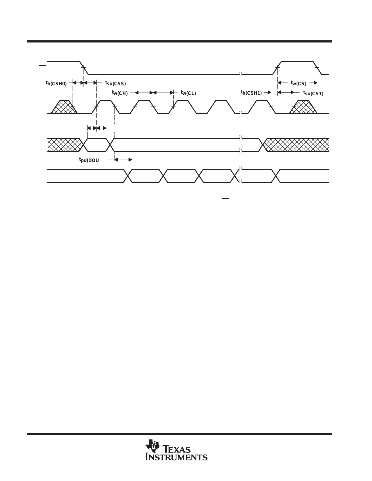
digital input timing requirements (see Figure 1)
PARAMETER MIN NOM MAX UNIT
t
su(DS)
t
h(DH)
t
su(CSS)
t
su(CS1)
t
h(CSH0)
t
h(CSH1)
t
w(CS)
t
w(CL)
t
w(CH)
output switching characteristic
t
pd(DOUT)
operating characteristics over recommended operating free-air temperature range, VDD = 5 V ±5%,
V
ref
Setup time, DIN before SCLK high 45 ns
Hold time, DIN valid after SCLK high 0 ns
Setup time, CS low to SCLK high 1 ns
Setup time, CS high to SCLK high 50 ns
Hold time, SCLK low to CS low 1 ns
Hold time, SCLK low to CS high 0 ns
Pulse duration, minimum chip select pulse width high 20 ns
Pulse duration, SCLK low 25 ns
Pulse duration, SCLK high 25 ns
PARAMETER TEST CONDITIONS MIN NOM MAX UNIT
Propagation delay time, DOUT CL = 50 pF 50 ns
= 2.048 V (unless otherwise noted)
analog output dynamic performance
PARAMETER TEST CONDITIONS MIN TYP MAX UNIT
SR Output slew rate
t
Output settling time
s
Glitch energy DIN = All 0s to all 1s 5
NOTE 10: Settling time is the time for the output signal to remain within ±0.5 LSB of the final measured value for a digital input code change of
000 hex to 3FF hex or 3FF hex to 000 hex.
CL = 100 pF,
TA = 25°C
To 0.5 LSB,
RL = 10 kΩ,
RL = 10 kΩ,
CL = 100 pF,
See Note 10
0.3 0.5 V/µs
12.5 µs
nVs
reference input (REFIN)
PARAMETER TEST CONDITIONS MIN TYP MAX UNIT
Reference feedthrough REFIN = 1 Vpp at 1 kHz + 2.048 Vdc (see Note 11) –80 dB
Reference input
bandwidth (f–3dB)
NOTE 11: Reference feedthrough is measured at the DAC output with an input code = 000 hex and a V
REFIN = 0.2 Vpp + 2.048 Vdc REFIN = 0.2 Vpp + 2.048 Vdc 30 kHz
input = 2.048 Vdc + 1 Vpp at 1 kHz.
ref
POST OFFICE BOX 655303 • DALLAS, TEXAS 75265
5
TLC5615C, TLC5615I
ÎÎÎ
ÎÎÎ
10-BIT DIGITAL-TO-ANALOG CONVERTERS
SLAS142C – OCTOBER 1996 – REVISED MARCH 2000
PARAMETER MEASUREMENT INFORMATION
CS
t
h(CSH0)
SCLK
See Note A See Note A
t
su(DS)
DIN
t
pd(DOUT)
DOUT
See Note B
NOTES: A. The input clock, applied at the SCLK terminal, should be inhibited low when CS is high to minimize clock feedthrough.
B. Data input from preceeding conversion cycle.
C. Sixteenth SCLK falling edge
Previous LSB
t
su(CSS)
t
w(CH)
t
h(DH)
t
w(CS)
t
w(CL)
MSB LSB
t
h(CSH1)
t
See Note C
su(CS1)
Figure 1. Timing Diagram
6
POST OFFICE BOX 655303 • DALLAS, TEXAS 75265

TLC5615C, TLC5615I
10-BIT DIGITAL-TO-ANALOG CONVERTERS
SLAS142C – OCTOBER 1996 – REVISED MARCH 2000
TYPICAL CHARACTERISTICS
OUTPUT SINK CURRENT
vs
OUTPUT PULLDOWN VOLTAGE
20
VDD = 5 V
18
V
= 2.048 V
REFIN
TA = 25°C
16
14
12
10
8
6
– Output Sink Current – mA
4
O
I
2
0
0.1 0.2 0.4 0.6
0.3 0.5 0.7 0.9 1.1
VO – Output Pulldown Voltage – V
OUTPUT SOURCE CURRENT
OUTPUT PULLUP VOLTAGE
30
VDD = 5 V
V
= 2.048 V
REFIN
25
TA = 25°C
20
15
10
– Output Source Current – mA
O
I
5
0
5
4.8 4.6
4.4 4.2 4
VO – Output Pullup Voltage – V
0.8 1
Figure 2
vs
3.8 3.6 3.4 3.2 3
1.2
Figure 3
POST OFFICE BOX 655303 • DALLAS, TEXAS 75265
7

TLC5615C, TLC5615I
10-BIT DIGITAL-TO-ANALOG CONVERTERS
SLAS142C – OCTOBER 1996 – REVISED MARCH 2000
TYPICAL CHARACTERISTICS
SUPPLY CURRENT
TEMPERATURE
280
240
Aµ
200
160
120
– Supply Current –
80
DD
I
VDD = 5 V
40
V
= 2.048 V
REFIN
TA = 25°C
0
–60 –40 – 20 0 20 40 60 80 100 120 140
t – Temperature – °C
vs
V
TO V
REFIN
(OUT)
RELATIVE GAIN
vs
INPUT FREQUENCY
4
VDD = 5 V
V
2
0
–2
–4
–6
–8
G – Relative Gain – dB
–10
–12
–14
1 100 1 k 10 k 100 k
= 0.2 VPP + 2.048 V dc
REFIN
TA = 25°C
fI – Input Frequency – Hz
Figure 5
Figure 4
70
60
50
40
30
20
Signal-To-Noise + Distortion – dB
10
0
1 k
SIGNAL-TO-NOISE + DISTORTION
vs
INPUT FREQUENCY AT REFIN
VDD = 5 V
TA = 25°C
V
= 4 V
REFIN
10 k 100 k 300 k
Frequency – Hz
Figure 6
PP
8
POST OFFICE BOX 655303 • DALLAS, TEXAS 75265

TLC5615C, TLC5615I
10-BIT DIGITAL-TO-ANALOG CONVERTERS
SLAS142C – OCTOBER 1996 – REVISED MARCH 2000
TYPICAL CHARACTERISTICS
0.2
0.15
0.1
0.05
0
–0.05
–0.1
–0.15
Differential Nonlinearity – LSB
–0.2
255 511 767 10230
Input Code
Figure 7. Differential Nonlinearity With Input Code
1
0.8
0.6
0.4
0.2
0
–0.2
–0.4
–0.6
Integral Nonlinearity – LSB
–0.8
–1
255 511 767 10230
Input Code
Figure 8. Integral Nonlinearity With Input Code
POST OFFICE BOX 655303 • DALLAS, TEXAS 75265
9

TLC5615C, TLC5615I
10-BIT DIGITAL-TO-ANALOG CONVERTERS
SLAS142C – OCTOBER 1996 – REVISED MARCH 2000
APPLICATION INFORMATION
general function
The TLC5615 uses a resistor string network buffered with an op amp in a fixed gain of 2 to convert 10-bit digital
data to analog voltage levels (see functional block diagram and Figure 9). The output of the TLC5615 is the
same polarity as the reference input (see Table 1).
An internal circuit resets the DAC register to all zeros on power up.
DIN SCLK CS
DOUT
REFIN
+
_
Resistor
String
DAC
AGND V
0.1 µF
Figure 9. TLC5615 Typical Operating Circuit
Table 1. Binary Code Table (0 V to 2 V
†
INPUT
1111 1111 11(00)
:
1000 0000 01(00)
1000 0000 00(00)
0111 1111 11(00)
:
0000 0000 01(00)
2ǒV
2ǒV
2
REFIN
2
2
R
DD
REFIN
REFIN
ǒ
V
REFIN
ǒ
V
REFIN
ǒ
V
REFIN
+
_
R
5 V
Output)
OUTPUT
1023
Ǔ
1024
:
513
Ǔ
1024
512
Ǔ
+
1024
511
Ǔ
1024
:
Ǔ
1024
1
V
REFIN
Gain = 2
,
OUT
10
0000 0000 00(00)
†
A 10-bit data word with two bits below the LSB bit (sub-LSB) with 0 values
must be written since the DAC input latch is 12 bits wide.
POST OFFICE BOX 655303 • DALLAS, TEXAS 75265
0 V

TLC5615C, TLC5615I
10-BIT DIGITAL-TO-ANALOG CONVERTERS
SLAS142C – OCTOBER 1996 – REVISED MARCH 2000
APPLICATION INFORMATION
buffer amplifier
The output buffer has a rail-to-rail output with short circuit protection and can drive a 2-kΩ load with a 100-pF
load capacitance. Settling time is 12.5 µs typical to within 0.5 LSB of final value.
external reference
The reference voltage input is buffered, which makes the DAC input resistance not code dependent. Therefore,
the REFIN input resistance is 10 MΩ and the REFIN input capacitance is typically 5 pF independent of input
code. The reference voltage determines the DAC full-scale output.
logic interface
The logic inputs function with either TTL or CMOS logic levels. However, using rail-to-rail CMOS logic achieves
the lowest power dissipation. The power requirement increases by approximately 2 times when using TTL logic
levels.
serial clock and update rate
Figure 1 shows the TLC5615 timing. The maximum serial clock rate is:
wǒCH
1
)
t
Ǔ
)
Ǔ
wǒCL
t
wǒCL
Ǔ
Ǔ
)
t
Ǔ
wǒCS
Ǔ
f
(SCLK)max
or approximately 14 MHz. The digital update rate is limited by the chip-select period, which is:
t
p(CS)
and is equal to 820 ns which is a 1.21 MHz update rate. However, the DAC settling time to 10 bits of 12.5 µs
limits the update rate to 80 kHz for full-scale input step transitions.
+
+16 ǒt
t
wǒCH
POST OFFICE BOX 655303 • DALLAS, TEXAS 75265
11

TLC5615C, TLC5615I
10-BIT DIGITAL-TO-ANALOG CONVERTERS
SLAS142C – OCTOBER 1996 – REVISED MARCH 2000
APPLICATION INFORMATION
serial interface
When chip select (CS) is low, the input data is read into a 16-bit shift register with the input data clocked in most
significant bit first. The rising edge of the SLCK input shifts the data into the input register.
The rising edge of CS then transfers the data to the DAC register. When CS is high, input data cannot be clocked
into the input register. All CS transitions should occur when the SCLK input is low.
If the daisy chain (cascading) function (see daisy-chaining devices section) is not used, a 12-bit input data
sequence with the MSB first can be used as shown in Figure 10:
12 Bits
10 Data Bits x x
MSB LSB 2 Extra (Sub-LSB) Bits
x = don’t care
Figure 10. 12-Bit Input Data Sequence
or 16 bits of data can be transferred as shown in Figure 11 with the 4 upper dummy bits first.
16 Bits
4 Upper Dummy Bits
MSB LSB 2 Extra (Sub-LSB) Bits
x = don’t care
10 Data Bits x x
Figure 11. 16-Bit Input Data Sequence
The data from DOUT requires 16 falling edges of the input clock and, therefore, requires an extra clock width.
When daisy chaining multiple TLC5615 devices, the data requires 4 upper dummy bits because the data
transfer requires 16 input-clock cycles plus one additional input-clock falling edge to clock out the data at the
DOUT terminal (see Figure 1).
The two extra (sub-LSB) bits are always required to provide hardware and software compatibility with 12-bit data
converter transfers.
The TLC5615 three-wire interface is compatible with the SPI, QSPI†, and Microwire serial standards. The
hardware connections are shown in Figure 12 and Figure 13.
The SPI and Microwire interfaces transfer data in 8-bit bytes, therefore, two write cycles are required to input
data to the DAC. The QSPI interface, which has a variable input data length from 8 to 16 bits, can load the DAC
input register in one write cycle.
†
CPOL = 0, CPHA = 0, QSPI protocol designations
12
POST OFFICE BOX 655303 • DALLAS, TEXAS 75265

serial interface (continued)
TLC5615C, TLC5615I
10-BIT DIGITAL-TO-ANALOG CONVERTERS
SLAS142C – OCTOBER 1996 – REVISED MARCH 2000
APPLICATION INFORMATION
SCLK
DIN
TLC5615
CS
DOUT
NOTE A: The DOUT-SI connection is not required for writing
to the TLC5615 but may be used for verifying data
transfer if desired.
SK
SO
I/O
SI
Microwire
Port
Figure 12. Microwire Connection
SCLK
DIN
TLC5615
CS
DOUT
NOTE A: The DOUT-MISO connection is not required for writing to
the TLC5615 but may be used for verifying data transfer.
Figure 13. SPI/QSPI Connection
SCK
MOSI
SPI/QSPI
Port
I/O
MISO
CPOL = 0, CPHA = 0
daisy-chaining devices
DACs can be daisy-chained by connecting the DOUT terminal of one device to the DIN of the next device in
the chain, providing that the setup time, t
time, t
, plus the propagation delay time, t
su(DS)
su(CSS)
, (CS low to SCLK high) is greater than the sum of the setup
pd(DOUT)
, for proper timing (see digital input timing requirements
section). The data at DIN appears at DOUT, delayed by 16 clock cycles plus one clock width. DOUT is a
totem-poled output for low power. DOUT changes on the SCLK falling edge when CS
is low. When CS is high,
DOUT remains at the value of the last data bit and does not go into a high-impedance state.
linearity, offset, and gain error using single ended supplies
When an amplifier is operated from a single supply , the voltage offset can still be either positive or negative. With
a positive offset, the output voltage changes on the first code change. With a negative offset the output voltage
may not change with the first code depending on the magnitude of the offset voltage.
The output amplifier attempts to drive the output to a negative voltage. However, because the most negative
supply rail is ground, the output cannot drive below ground and clamps the output at 0 V.
The output voltage then remains at zero until the input code value produces a sufficient positive output voltage
to overcome the negative offset voltage, resulting in the transfer function shown in Figure 14.
Output
Voltage
0 V
Negative
Offset
DAC Code
Figure 14. Effect of Negative Offset (Single Supply)
POST OFFICE BOX 655303 • DALLAS, TEXAS 75265
13

TLC5615C, TLC5615I
10-BIT DIGITAL-TO-ANALOG CONVERTERS
SLAS142C – OCTOBER 1996 – REVISED MARCH 2000
APPLICATION INFORMATION
linearity, offset, and gain error using single ended supplies (continued)
This offset error , not the linearity error, produces this breakpoint. The transfer function would have followed the
dotted line if the output buffer could drive below the ground rail.
For a DAC, linearity is measured between zero-input code (all inputs 0) and full-scale code (all inputs 1) after
offset and full scale are adjusted out or accounted for in some way . However , single supply operation does not
allow for adjustment when the offset is negative due to the breakpoint in the transfer function. So the linearity
is measured between full-scale code and the lowest code that produces a positive output voltage. For the
TLC5615, the zero-scale (offset) error is plus or minus 3 LSB maximum. The code is calculated from the
maximum specification for the negative offset.
power-supply bypassing and ground management
Printed-circuit boards that use separate analog and digital ground planes offer the best system performance.
Wire-wrap boards do not perform well and should not be used. The two ground planes should be connected
together at the low-impedance power-supply source. The best ground connection may be achieved by
connecting the DAC AGND terminal to the system analog ground plane making sure that analog ground
currents are well managed and there are negligible voltage drops across the ground plane.
A 0.1-µF ceramic-capacitor bypass should be connected between V
and AGND and mounted with short leads
DD
as close as possible to the device. Use of ferrite beads may further isolate the system analog supply from the
digital power supply.
Figure 15 shows the ground plane layout and bypassing technique.
Analog Ground Plane
1
2
3
4
8
7
6
5
0.1 µF
Figure 15. Power-Supply Bypassing
saving power
Setting the DAC register to all 0s minimizes power consumption by the reference resistor array and the output
load when the system is not using the DAC.
ac considerations
digital feedthrough
Even with CS
DAC package internal stray capacitance and appear at the DAC analog output as digital feedthrough. Digital
feedthrough is tested by holding CS
high, high-speed serial data at any of the digital input or output terminals may couple through the
high and transmitting 0101010101 from DIN to DOUT.
analog feedthrough
Higher frequency analog input signals may couple to the output through internal stray capacitance. Analog
feedthrough is tested by holding CS
high, setting the DAC code to all 0s, sweeping the frequency applied to
REFIN, and monitoring the DAC output.
14
POST OFFICE BOX 655303 • DALLAS, TEXAS 75265

TLC5615C, TLC5615I
10-BIT DIGITAL-TO-ANALOG CONVERTERS
SLAS142C – OCTOBER 1996 – REVISED MARCH 2000
MECHANICAL DATA
D (R-PDSO-G**) PLASTIC SMALL-OUTLINE PACKAGE
14 PINS SHOWN
0.050 (1,27)
14
1
0.069 (1,75) MAX
A
0.020 (0,51)
0.014 (0,35)
0.010 (0,25)
0.004 (0,10)
DIM
8
7
PINS **
0.010 (0,25)
0.157 (4,00)
0.150 (3,81)
M
0.244 (6,20)
0.228 (5,80)
Seating Plane
0.004 (0,10)
8
14
0.008 (0,20) NOM
0°–8°
16
Gage Plane
0.010 (0,25)
0.044 (1,12)
0.016 (0,40)
A MAX
A MIN
NOTES: A. All linear dimensions are in inches (millimeters).
B. This drawing is subject to change without notice.
C. Body dimensions do not include mold flash or protrusion, not to exceed 0.006 (0,15).
D. Falls within JEDEC MS-012
POST OFFICE BOX 655303 • DALLAS, TEXAS 75265
0.197
(5,00)
0.189
(4,80)
0.344
(8,75)
0.337
(8,55)
0.394
(10,00)
0.386
(9,80)
4040047/D 10/96
15

MECHANICAL DATA
MPDI001A – JANUARY 1995 – REVISED JUNE 1999
MECHANICAL DATA
P (R-PDIP-T8) PLASTIC DUAL-IN-LINE
0.400 (10,60)
0.355 (9,02)
8
5
0.260 (6,60)
0.240 (6,10)
1
0.021 (0,53)
0.015 (0,38)
NOTES: A. All linear dimensions are in inches (millimeters).
B. This drawing is subject to change without notice.
C. Falls within JEDEC MS-001
4
0.070 (1,78) MAX
0.020 (0,51) MIN
0.200 (5,08) MAX
0.125 (3,18) MIN
0.100 (2,54)
0.010 (0,25)
Seating Plane
M
0.325 (8,26)
0.300 (7,62)
0.015 (0,38)
Gage Plane
0.010 (0,25) NOM
0.430 (10,92)
MAX
4040082/D 05/98
For the latest package information, go to http://www.ti.com/sc/docs/package/pkg_info.htm
16
POST OFFICE BOX 655303 • DALLAS, TEXAS 75265

MPDI001A – JANUARY 1995 – REVISED JUNE 1999
MECHANICAL DATA
MECHANICAL DATA
DGK (R-PDSO-G8) PLASTIC SMALL-OUTLINE PACKAGE
0,65
8
1
1,07 MAX
3,05
2,95
0,38
0,25
5
3,05
2,95
4
Seating Plane
0,15
0,05
0,25
4,98
4,78
M
0,10
0,15 NOM
Gage Plane
0°–6°
0,25
0,69
0,41
NOTES: A. All linear dimensions are in millimeters.
B. This drawing is subject to change without notice.
C. Body dimensions do not include mold flash or protrusion.
D. Falls within JEDEC MO-187
For the latest package information, go to http://www.ti.com/sc/docs/package/pkg_info.htm
4073329/B 04/98
POST OFFICE BOX 655303 • DALLAS, TEXAS 75265
17

IMPORTANT NOTICE
T exas Instruments and its subsidiaries (TI) reserve the right to make changes to their products or to discontinue
any product or service without notice, and advise customers to obtain the latest version of relevant information
to verify, before placing orders, that information being relied on is current and complete. All products are sold
subject to the terms and conditions of sale supplied at the time of order acknowledgement, including those
pertaining to warranty, patent infringement, and limitation of liability.
TI warrants performance of its semiconductor products to the specifications applicable at the time of sale in
accordance with TI’s standard warranty. Testing and other quality control techniques are utilized to the extent
TI deems necessary to support this warranty . Specific testing of all parameters of each device is not necessarily
performed, except those mandated by government requirements.
CERTAIN APPLICA TIONS USING SEMICONDUCT OR PRODUCTS MAY INVOLVE POTENTIAL RISKS OF
DEATH, PERSONAL INJURY, OR SEVERE PROPERTY OR ENVIRONMENTAL DAMAGE (“CRITICAL
APPLICATIONS”). TI SEMICONDUCTOR PRODUCTS ARE NOT DESIGNED, AUTHORIZED, OR
WARRANTED TO BE SUITABLE FOR USE IN LIFE-SUPPORT DEVICES OR SYSTEMS OR OTHER
CRITICAL APPLICA TIONS. INCLUSION OF TI PRODUCTS IN SUCH APPLICATIONS IS UNDERST OOD TO
BE FULLY AT THE CUSTOMER’S RISK.
In order to minimize risks associated with the customer’s applications, adequate design and operating
safeguards must be provided by the customer to minimize inherent or procedural hazards.
TI assumes no liability for applications assistance or customer product design. TI does not warrant or represent
that any license, either express or implied, is granted under any patent right, copyright, mask work right, or other
intellectual property right of TI covering or relating to any combination, machine, or process in which such
semiconductor products or services might be or are used. TI’s publication of information regarding any third
party’s products or services does not constitute TI’s approval, warranty or endorsement thereof.
Copyright 2000, Texas Instruments Incorporated
 Loading...