

TLC352
LinCMOS DUAL DIFFERENTIAL COMPARATOR
SLCS016 – SEPTEMBER 1985 – REVISED OCTOBER 1990
1
POST OFFICE BOX 655303 • DALLAS, TEXAS 75265
D
Single- or Dual-Supply Operation
D
Wide Range of Supply Voltages
1.5 V to 18 V
D
Very Low Supply Current Drain
150 µA Typ at 5 V
65 µA Typ at 1.4 V
D
Built-In ESD Protection
D
High Input Impedance...10
12
Ω Typ
D
Extremely Low Input Bias Current 5 pA Typ
D
Ultrastable Low Input Offset Voltage
D
Input Offset Voltage Change at Worst-Case
Input Conditions Typically 0.23 µV/ Month,
Including the First 30 Days
D
Common-Mode Input Voltage Range
Includes Ground
D
Outputs Compatible With TTL, MOS, and
CMOS
D
Pin-Compatible With LM393
description
This device is fabricated using LinCMOS
technology and consists of two independent
voltage comparators, each designed to operate
from a single power supply. Operation from dual
supplies is also possible if the difference between
the two supplies is 1.4 V to 18 V. Each device
features extremely high input impedance
(typically greater than 10
12
Ω), which allows direct
interface to high-impedance sources. The output
are n-channel open-drain configurations and can
be connected to achieve positive-logic wired-AND
relationships. The capability of the TLC352 to
operate from 1.4-V supply makes this device ideal
for low-voltage battery applications.
The TLC352 has internal electrostatic discharge (ESD) protection circuits and has been classified with a 2000-V
ESD rating tested under MIL-STD-883C, Method 3015. However, care should be exercised in handling this
device as exposure to ESD may result in degradation of the device parametric performance.
The TLC352C is characterized for operation from 0°C to 70°C. The TLC352I is characterized for operation over
the industrial temperature range of – 40°C to 85°C. The TLC352M is characterized for operation over the full
military temperature range – 55°C to 125°C.
Copyright 1990, Texas Instruments Incorporated
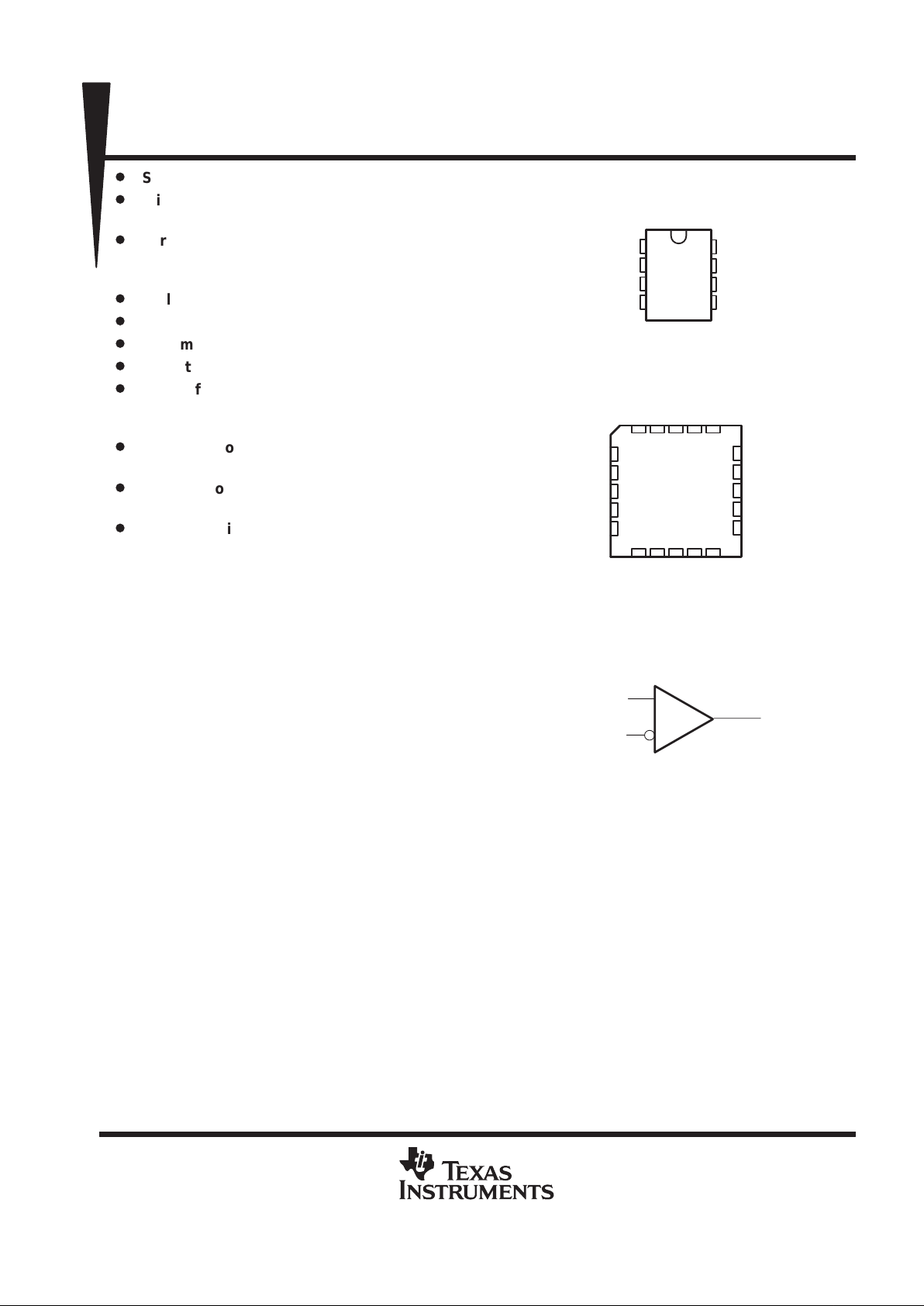
TLC352C, TLC352I ...D OR P PACKAGE
TLC352M . . . JG PACKAGE
(TOP VIEW)
TLC352M . . . FK PACKAGE
(TOP VIEW)
1
2
3
4
8
7
6
5
1OUT
1IN–
1IN+
GND
V
DD
2OUT
2IN–
2IN+
OUT
symbol (each comparator)
IN+
3212019
910111213
4
5
6
7
8
18
17
16
15
14
NC
2OUT
NC
2IN–
NC
NC
1IN–
NC
1IN+
NC
NC
1OUT
NC
2IN+
NC
NC
NC
GND
NC
NC — No Internal connection
V
DD
IN–
PRODUCTION DATA information is current as of publication date.
Products conform to specifications per the terms of Texas Instruments
standard warranty. Production processing does not necessarily include
testing of all parameters.
LinCMOS is a trademark of Texas Instruments Incorporated.
TLC352
LinCMOS DUAL DIFFERENTIAL COMPARATOR
SLCS016 – SEPTEMBER 1985 – REVISED OCTOBER 1990
2
POST OFFICE BOX 655303 • DALLAS, TEXAS 75265
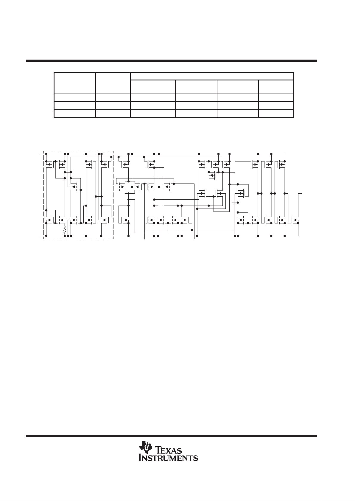
AVAILABLE OPTIONS
PACKAGE
T
A
V
IO
max
AT 25°C
SMALL-OUTLINE
(D)
CHIP-CARRIER
(FK)
CERAMIC DIP
(JG)
PLASTIC DIP
(P)
0°C to 70°C 5 mV TLC352CD — — TLC352CP
– 40°C to 85°C 5 mV TLC352ID — — TLC352IP
– 55°C to 125°C 5 mV — TLC352MFK TLC352MJG —
The D packages are available taped and reeled. Add R suffix to device type (e.g., TLC352 CDR).
equivalent schematic (each comparator)
Common to All Channels
V
DD
GND
OUT
IN+
IN–
TLC352
LinCMOS DUAL DIFFERENTIAL COMPARATOR
SLCS016 – SEPTEMBER 1985 – REVISED OCTOBER 1990
3
POST OFFICE BOX 655303 • DALLAS, TEXAS 75265
absolute maximum ratings over operating free-air temperature range (unless otherwise noted)
†
Supply voltage, V
DD
(see Note 1) 18 V. . . . . . . . . . . . . . . . . . . . . . . . . . . . . . . . . . . . . . . . . . . . . . . . . . . . . . . . . . . .
Differential input voltage, V
ID
(see Note 2) ± 18 V. . . . . . . . . . . . . . . . . . . . . . . . . . . . . . . . . . . . . . . . . . . . . . . . . .
Input voltage, V
I
V
DD
. . . . . . . . . . . . . . . . . . . . . . . . . . . . . . . . . . . . . . . . . . . . . . . . . . . . . . . . . . . . . . . . . . . . . . . . . . .
Input voltage range, V
I
– 0.3 V to 18 V. . . . . . . . . . . . . . . . . . . . . . . . . . . . . . . . . . . . . . . . . . . . . . . . . . . . . . . . . . . . .
Output voltage, V
O
18 V. . . . . . . . . . . . . . . . . . . . . . . . . . . . . . . . . . . . . . . . . . . . . . . . . . . . . . . . . . . . . . . . . . . . . . . . .
Input current, I
I
± 5 mA. . . . . . . . . . . . . . . . . . . . . . . . . . . . . . . . . . . . . . . . . . . . . . . . . . . . . . . . . . . . . . . . . . . . . . . . . .
Output current, I
O
20 mA. . . . . . . . . . . . . . . . . . . . . . . . . . . . . . . . . . . . . . . . . . . . . . . . . . . . . . . . . . . . . . . . . . . . . . . .
Duration of output short circuit to ground (see Note 3) unlimited. . . . . . . . . . . . . . . . . . . . . . . . . . . . . . . . . . . . . .
Continuous total dissipation See Dissipation Rating Table. . . . . . . . . . . . . . . . . . . . . . . . . . . . . . . . . . . . . . . . . . .
Operating free-air temperature range, T
A
TLC352C 0°C to 70°C. . . . . . . . . . . . . . . . . . . . . . . . . . . . . . . . . . . . .
TLC352I – 40°C to 85°C. . . . . . . . . . . . . . . . . . . . . . . . . . . . . . . . . . . .
TLC352M – 55°C to 125°C. . . . . . . . . . . . . . . . . . . . . . . . . . . . . . . . .
Storage temperature range – 65°C to 150°C. . . . . . . . . . . . . . . . . . . . . . . . . . . . . . . . . . . . . . . . . . . . . . . . . . . . . . .
Case temperature for 60 seconds: FK package 260°C. . . . . . . . . . . . . . . . . . . . . . . . . . . . . . . . . . . . . . . . . . . . . .
Lead temperature 1,6 mm (1/16 inch) from case for 60 seconds: JG package 300°C. . . . . . . . . . . . . . . . . . . .
Lead temperature 1,6 mm (1/16 inch) from case for 10 seconds: D or P package 260°C. . . . . . . . . . . . . . . . .
†
Stresses beyond those listed under “absolute maximum ratings” may cause permanent damage to the device. These are stress ratings only, and
functional operation of the device at these or any other conditions beyond those indicated under “recommended operating conditions” is not
implied. Exposure to absolute-maximum-rated conditions for extended periods may affect device reliability.
NOTES: 1. All voltage values except differential voltages are with respect to the network ground.
2. Differential voltages are at IN+ with respect to IN –.
3. Short circuits from outputs to VDD can cause excessive heating and eventual device destruction.
DISSIPATION RATING T ABLE
PACKAGE
TA ≤ 25°C
POWER RATING
DERATING
FACTOR
DERATE
ABOVE T
A
TA = 70°C
POWER RATING
TA = 85°C
POWER RATING
TA = 125°C
POWER RATING
D
FK
JG
P
500 mW
500 mW
500 mW
500 mW
5.8 mW/°C
11.0 mW/°C
8.4 mW/°C
N/A
64°C
104°C
90°C
N/A
464 mW
500 mW
500 mW
500 mW
377 mW
500 mW
500 mW
500 mW
N/A
275 mW
210 mW
N/A

Template Release Date: 7–11–94
TLC352
LinCMOS DUAL DIFFERENTIAL COMPARATOR
TM
SLCS016 – SEPTEMBER 1985 – REVISED OCTOBER 1990
4
POST OFFICE BOX 655303 DALLAS, TEXAS 75265
•
recommended operating conditions
TLC352C TLC352I TLC352M
MIN MAX MIN MAX MIN MAX
UNIT
Supply voltage, V
DD
1.4 16 1.4 16 1.4 16 V
p
VDD = 5 V 0 3.5 0 3.5 0 3.5
Common-mode input voltage, V
IC
VDD = 10 V 0 8.5 0 8.5 0 8.5
V
Operating free-air temperature, T
A
0 70 – 40 85 – 55 125 °C
electrical characteristics at specified free-air temperature, VDD = 1.4 V (unless otherwise noted)
TLC352C TLC352I TLC352M
PARAMETER
TEST CONDITIONS
T
A
†
MIN TYP MAX MIN TYP MAX MIN TYP MAX
UNIT
p
25°C 2 5 2 5 2 5
VIOInput offset voltage
V
IC
=
V
ICR
min
,
See Note 4
Full range 6.5 7 10
mV
p
25°C 1 1 1 pA
IIOInput offset current
MAX 0.3 1 10 nA
p
25°C 5 5 5 pA
IIBInput bias current
MAX 0.6 2 20 nA
V
ICR
Common-mode input voltage
range
Full range
0 to
0.2
0 to
0.2
0 to
0.2
V
p
25°C 100 200 100 200 100 200
VOLLow-level output voltage
Full range 200 200 200
mV
I
OL
Low-level output current VID = – 0.5 V, VOL = 0.3 V 25°C 1 1.6 1 1.6 1 1.6 mA
pp
p
25°C 65 150 65 150 65 150
IDDSupply current (two comparators)
V
ID
= 0.5 V,
No load
Full range 200 200 200
µ
A
†
All characteristics are measured with zero common-mode input voltage unless otherwise noted. Full range is 0°C to 70°C for TLC352C, – 40°C to 85°C for TLC352I, – 55°C to 125°C
for TLC352M. IMPORTANT: See Parameter Measurement Information.
NOTE 4: The offset voltage limits given are the maximum values required to drive the output above 1.25 V or below 150 mV with a 10-kΩ resistor between the output and VDD. They
can be verified by applying the limit value to the input and checking for the appropriate output state.

TLC352
LinCMOS DUAL DIFFERENTIAL COMPARATOR
TM
SLCS016 – SEPTEMBER 1985 – REVISED OCTOBER 1990
POST OFFICE BOX 655303 DALLAS, TEXAS 75265
• 5
electrical characteristics at specified free-air temperature, VDD = 5 V (unless otherwise noted)
TLC352C TLC352I TLC352M
PARAMETER
TEST CONDITIONS
T
A
†
MIN TYP MAX MIN TYP MAX MIN TYP MAX
UNIT
p
25°C 1 5 1 5 1 5
VIOInput offset voltage
V
IC
=
V
ICR
min
,
See Note 5
Full range 6.5 7 10
mV
p
25°C 1 1 1 pA
IIOInput offset current
MAX 0.3 1 10 nA
p
25°C 5 5 5 pA
IIBInput bias current
MAX 0.6 2 20 nA
Common-mode
25°C
0 to
VDD – 1
0 to
VDD – 1
0 to
VDD – 1
V
ICR
input voltage range
Full range
0 to
VDD – 1.5
0 to
VDD – 1.5
0 to
VDD – 1.5
V
High-level output
VOH = 5 V 25°C 0.1 0.1 0.1 nA
I
OH
g
current
V
ID
= 1
V
VOH = 15 V Full range 1 1 1 µA
Low-level output
25°C 150 400 150 400 150 400
V
OL
voltage
V
ID
= 1 V,
I
OL
= 4
mA
Full range 700 700 700
mV
I
OL
Low-level output
current
VID = – 1 V, VOL = 1.5 V 25°C 6 16 6 16 6 16 mA
Supply current
25°C 0.15 0.3 0.15 0.3 0.15 0.3
I
DD
y
(two comparators)
V
ID
= 1 V,
No load
Full range 0.4 0.4 0.4
mA
†
All characteristics are measured with zero common-mode input voltage unless otherwise noted. Full range is 0°C to 70°C for TLC352C, – 40°C to 85°C for TLC352I, – 55°C to 125°C
for TLC352M. IMPORTANT: See Parameter Measurement Information.
NOTE 5: The offset voltage limits given are the maximum values required to drive the output above 4 V or below 400 mV with a 10- kΩ resistor between the output and VDD. They
can be verified by applying the limit value to the input and checking for the appropriate output state.
switching characteristics, VDD = 5 V, TA = 25°C
PARAMETER TEST CONDITIONS
TLC352C, TLC352I
TLC352M
UNIT
MIN TYP MAX
p
RL connected to 5 V through 5.1 kΩ,, 100-mV input step with 5-mV overdrive 650
Response time
CL = 15 pF‡, See Note 6 TTL-level input step 200
ns
‡
CL includes probe and jig capacitance.
NOTE 6: The response time specified is the interval between the input step function and the instant when the output crosses 1.4 V.

TLC352
LinCMOS DUAL DIFFERENTIAL COMPARATOR
SLCS016 – SEPTEMBER 1985 – REVISED OCTOBER 1990
6
POST OFFICE BOX 655303 • DALLAS, TEXAS 75265
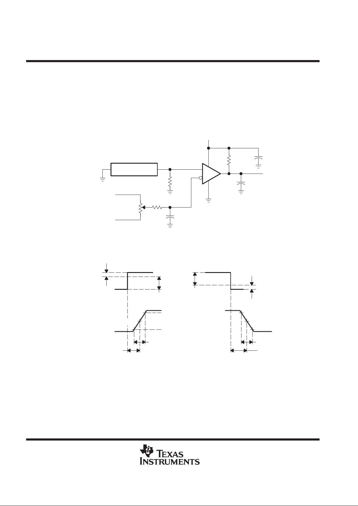
PARAMETER MEASUREMENT INFORMATION
The digital output stage of the TLC352 can be damaged if it is held in the linear region of the transfer curve.
Conventional operational amplifier/comparator testing incorporates the use of a servo loop that is designed to force
the device output to a level within this linear region. Since the servo-loop method of testing cannot be used, the
following alternative for measuring parameters such as input offset voltage, common-mode rejection, etc., are
offered.
To verify that the input offset voltage falls within the limits specified, the limit value is applied to the input as shown
in Figure 1(a). With the noninverting input positive with respect to the inverting input, the output should be high. With
the input polarity reversed, the output should be low.
A similar test can be made to verify the input offset voltage at the common-mode extremes. The supply voltages can
be slewed as shown in Figure 1(b) for the V
ICR
test, rather than changing the input voltages, to provide greater
accuracy.
A close approximation of the input offset voltage can be obtained by using a binary search method to vary the
differential input voltage while monitoring the output state. When the applied input voltage differential is equal but
opposite in polarity to the input offset voltage, the output changes state.
+
–
Applied V
IO
Limit
V
O
5 V
5.1 kΩ
Applied V
IO
Limit
V
O
1 V
5.1 kΩ
– 4 V
(a) VIO WITH VIC = 0 (b) VIO WITH VIC = 4 V
+
–
Figure 1. Method for Verifying That Input Offset Voltage Is Within Specified Limits

TLC352
LinCMOS DUAL DIFFERENTIAL COMPARATOR
SLCS016 – SEPTEMBER 1985 – REVISED OCTOBER 1990
7
POST OFFICE BOX 655303 • DALLAS, TEXAS 75265
PARAMETER INFORMATION
Figure 2 illustrates a practical circuit for direct dc measurement of input offset voltage that does not bias the
comparator into the linear region. The circuit consists of a switching-mode servo loop in which U1a generates a
triangular waveform of approximately 20-mV amplitude. U1b acts as a buffer , with C2 and R4 removing any residual
dc offset. The signal is then applied to the inverting input of the comparator under test, while the noninverting input
is driven by the output of the integrator formed by U1c through the voltage divider formed by R9 and R10. The loop
reaches a stable operating point when the output of the comparator under test has a duty cycle of exactly 50%, which
can only occur when the incoming triangle wave is sliced symmetrically or when the voltage at the noninverting input
exactly equals the input offset voltage.
Voltage divider R9 and R10 provides a step up of the input offset voltage by a factor of 100 to make measurement
easier. The values of R5, R8, R9, and R10 can significantly influence the accuracy of the reading; therefore, it is
suggested that their tolerance level be 1% or lower.
Measuring the extremely low values of input current requires isolation from all other sources of leakage current and
compensation for the leakage of the test socket and board. With a good picoammeter, the socket and board leakage
can be measured with no device in the socket. Subsequently , this open-socket leakage value can be subtracted from
the measurement obtained with a device in the socket to obtain the actual input current of the device.
+
–
+
–
+
–
DUT
V
DD
R5
1.8 kΩ, 1%
C3 0.68 µF
U1c
1/4 TLC274CN
R7
1MΩ
R8
1.8 kΩ, 1%
R9
10 kΩ, 1%
R2
10 kΩ
R1
240 kΩ
Triangle
Generator
Integrator
U1b
1/4 TLC274CN
Buffer
C2
1 µF
R10
100 Ω, 1%
R3
100 kΩ
V
IO
(X100)
C4
0.1 µF
R6
5.1 kΩ
U1a
1/4 TLC274CN
R4
47 kΩ
C1
0.1 µF
Figure 2. Circuit for Input Offset Voltage Measurement
TLC352
LinCMOS DUAL DIFFERENTIAL COMPARATOR
SLCS016 – SEPTEMBER 1985 – REVISED OCTOBER 1990
8
POST OFFICE BOX 655303 • DALLAS, TEXAS 75265
PARAMETER MEASUREMENT INFORMATION
Response time is defined as the interval between the application of an input step function and the instant when the
output reaches 50% of its maximum value. Response time, low-to-high-level output, is measured from the leading
edge of the input pulse, while response time, high-to-low level output, is measured from the trailing edge of the input
pulse. Response-time measurement at low input signal levels can be greatly affected by the input offset voltage. The
offset voltage should be balanced by the adjustment at the inverting input (as shown in Figure 3) so that the circuit
is just at the transition point. Then a low signal, for example 105-mV or 5-mV overdrive, causes the output to change
state.
10%
50%
50 %
Pulse Generator
V
DD
10 Ω
10 Turn
1 V
–1 V
1 kΩ
0.1 mF
C
L
(see Note A)
1 µF5.1 kΩ
50 Ω
Input
Offset Voltage
Compensation
Adjustment
TEST CIRCUIT
t
PLH
90%
10%
t
PHL
t
f
t
r
90%
Input
Overdrive
Overdrive
Input
Low-to-High-
Level Output
High-to-LowLevel Output
100 mV
100 mV
VOLTAGE WAVEFORMS
DUT
NOTE A: CL includes probe and jig capacitance.
Figure 3. Response, Rise, and Fall Times Circuit and Voltage Waveforms

IMPORTANT NOTICE
T exas Instruments and its subsidiaries (TI) reserve the right to make changes to their products or to discontinue
any product or service without notice, and advise customers to obtain the latest version of relevant information
to verify, before placing orders, that information being relied on is current and complete. All products are sold
subject to the terms and conditions of sale supplied at the time of order acknowledgement, including those
pertaining to warranty, patent infringement, and limitation of liability.
TI warrants performance of its semiconductor products to the specifications applicable at the time of sale in
accordance with TI’s standard warranty. Testing and other quality control techniques are utilized to the extent
TI deems necessary to support this warranty. Specific testing of all parameters of each device is not necessarily
performed, except those mandated by government requirements.
CERT AIN APPLICATIONS USING SEMICONDUCTOR PRODUCTS MAY INVOLVE POTENTIAL RISKS OF
DEATH, PERSONAL INJURY, OR SEVERE PROPERTY OR ENVIRONMENTAL DAMAGE (“CRITICAL
APPLICATIONS”). TI SEMICONDUCTOR PRODUCTS ARE NOT DESIGNED, AUTHORIZED, OR
WARRANTED TO BE SUITABLE FOR USE IN LIFE-SUPPORT DEVICES OR SYSTEMS OR OTHER
CRITICAL APPLICATIONS. INCLUSION OF TI PRODUCTS IN SUCH APPLICA TIONS IS UNDERST OOD TO
BE FULLY AT THE CUSTOMER’S RISK.
In order to minimize risks associated with the customer’s applications, adequate design and operating
safeguards must be provided by the customer to minimize inherent or procedural hazards.
TI assumes no liability for applications assistance or customer product design. TI does not warrant or represent
that any license, either express or implied, is granted under any patent right, copyright, mask work right, or other
intellectual property right of TI covering or relating to any combination, machine, or process in which such
semiconductor products or services might be or are used. TI’s publication of information regarding any third
party’s products or services does not constitute TI’s approval, warranty or endorsement thereof.
Copyright 1998, Texas Instruments Incorporated
 Loading...