

Page 1
TLC320AD81C
Stereo Audio Digital Equalizer DAC
Data Manual
1999 Mixed Signal Linear Products
Page 2

Printed in U.S.A.
03/99
SLAS203
Page 3

TLC320AD81C
Stereo Audio Digital Equalizer DAC
SLAS203
March 1999
Printed on Recycled Paper
Page 4

IMPORTANT NOTICE
T exas Instruments and its subsidiaries (TI) reserve the right to make changes to their products or to discontinue
any product or service without notice, and advise customers to obtain the latest version of relevant information
to verify, before placing orders, that information being relied on is current and complete. All products are sold
subject to the terms and conditions of sale supplied at the time of order acknowledgement, including those
pertaining to warranty, patent infringement, and limitation of liability.
TI warrants performance of its semiconductor products to the specifications applicable at the time of sale in
accordance with TI’s standard warranty. Testing and other quality control techniques are utilized to the extent
TI deems necessary to support this warranty . Specific testing of all parameters of each device is not necessarily
performed, except those mandated by government requirements.
CERTAIN APPLICATIONS USING SEMICONDUCTOR PRODUCTS MAY INVOLVE POTENTIAL RISKS OF
DEATH, PERSONAL INJURY, OR SEVERE PROPERTY OR ENVIRONMENTAL DAMAGE (“CRITICAL
APPLICATIONS”). TI SEMICONDUCTOR PRODUCTS ARE NOT DESIGNED, AUTHORIZED, OR
WARRANTED TO BE SUITABLE FOR USE IN LIFE-SUPPORT DEVICES OR SYSTEMS OR OTHER
CRITICAL APPLICA TIONS. INCLUSION OF TI PRODUCTS IN SUCH APPLICATIONS IS UNDERST OOD TO
BE FULLY AT THE CUSTOMER’S RISK.
In order to minimize risks associated with the customer’s applications, adequate design and operating
safeguards must be provided by the customer to minimize inherent or procedural hazards.
TI assumes no liability for applications assistance or customer product design. TI does not warrant or represent
that any license, either express or implied, is granted under any patent right, copyright, mask work right, or other
intellectual property right of TI covering or relating to any combination, machine, or process in which such
semiconductor products or services might be or are used. TI’s publication of information regarding any third
party’s products or services does not constitute TI’s approval, warranty or endorsement thereof.
Copyright 1999, Texas Instruments Incorporated
Page 5

Contents
Section Title Page
1 Introduction 1–1. . . . . . . . . . . . . . . . . . . . . . . . . . . . . . . . . . . . . . . . . . . . . . . . . . . . . . . . . . . . . . .
1.1 Features 1–2. . . . . . . . . . . . . . . . . . . . . . . . . . . . . . . . . . . . . . . . . . . . . . . . . . . . . . . . . . . . . .
1.2 Functional Block Diagram 1–2. . . . . . . . . . . . . . . . . . . . . . . . . . . . . . . . . . . . . . . . . . . . . . .
1.3 Terminal Assignments 1–3. . . . . . . . . . . . . . . . . . . . . . . . . . . . . . . . . . . . . . . . . . . . . . . . . .
1.4 Ordering Information 1–3. . . . . . . . . . . . . . . . . . . . . . . . . . . . . . . . . . . . . . . . . . . . . . . . . . .
1.5 Terminal Functions 1–4. . . . . . . . . . . . . . . . . . . . . . . . . . . . . . . . . . . . . . . . . . . . . . . . . . . . .
2 Description 2–1. . . . . . . . . . . . . . . . . . . . . . . . . . . . . . . . . . . . . . . . . . . . . . . . . . . . . . . . . . . . . . .
2.1 Serial Audio Interface 2–1. . . . . . . . . . . . . . . . . . . . . . . . . . . . . . . . . . . . . . . . . . . . . . . . . .
2.2 Audio Processing 2–1. . . . . . . . . . . . . . . . . . . . . . . . . . . . . . . . . . . . . . . . . . . . . . . . . . . . . .
2.3 Power Supply 2–1. . . . . . . . . . . . . . . . . . . . . . . . . . . . . . . . . . . . . . . . . . . . . . . . . . . . . . . . .
2.4 DAC 2–1. . . . . . . . . . . . . . . . . . . . . . . . . . . . . . . . . . . . . . . . . . . . . . . . . . . . . . . . . . . . . . . . .
2.5 Serial Audio Interface 2–2. . . . . . . . . . . . . . . . . . . . . . . . . . . . . . . . . . . . . . . . . . . . . . . . . .
2.5.1 I
2.5.2 Protocol 2–2. . . . . . . . . . . . . . . . . . . . . . . . . . . . . . . . . . . . . . . . . . . . . . . . . . . . . . .
2.5.3 Implementation 2–2. . . . . . . . . . . . . . . . . . . . . . . . . . . . . . . . . . . . . . . . . . . . . . . . .
2.5.4 Timing 2–2. . . . . . . . . . . . . . . . . . . . . . . . . . . . . . . . . . . . . . . . . . . . . . . . . . . . . . . .
2.6 Left-Justified Serial Format 2–3. . . . . . . . . . . . . . . . . . . . . . . . . . . . . . . . . . . . . . . . . . . . . .
2.6.1 Protocol 2–3. . . . . . . . . . . . . . . . . . . . . . . . . . . . . . . . . . . . . . . . . . . . . . . . . . . . . . .
2.6.2 Implementation 2–3. . . . . . . . . . . . . . . . . . . . . . . . . . . . . . . . . . . . . . . . . . . . . . . . .
2.6.3 Timing 2–3. . . . . . . . . . . . . . . . . . . . . . . . . . . . . . . . . . . . . . . . . . . . . . . . . . . . . . . .
2.7 Right-Justified Serial Format 2–4. . . . . . . . . . . . . . . . . . . . . . . . . . . . . . . . . . . . . . . . . . . .
2.7.1 Protocol 2–4. . . . . . . . . . . . . . . . . . . . . . . . . . . . . . . . . . . . . . . . . . . . . . . . . . . . . . .
2.7.2 Implementation 2–4. . . . . . . . . . . . . . . . . . . . . . . . . . . . . . . . . . . . . . . . . . . . . . . . .
2.7.3 Timing 2–4. . . . . . . . . . . . . . . . . . . . . . . . . . . . . . . . . . . . . . . . . . . . . . . . . . . . . . . .
2.8 Serial Control Interface 2–5. . . . . . . . . . . . . . . . . . . . . . . . . . . . . . . . . . . . . . . . . . . . . . . . .
2.8.1 I
2.8.2 Operation 2–6. . . . . . . . . . . . . . . . . . . . . . . . . . . . . . . . . . . . . . . . . . . . . . . . . . . . . .
2.9 Filter Processor 2–7. . . . . . . . . . . . . . . . . . . . . . . . . . . . . . . . . . . . . . . . . . . . . . . . . . . . . . . .
2.9.1 Biquad Block 2–7. . . . . . . . . . . . . . . . . . . . . . . . . . . . . . . . . . . . . . . . . . . . . . . . . . .
2.9.2 Filter Coefficients 2–7. . . . . . . . . . . . . . . . . . . . . . . . . . . . . . . . . . . . . . . . . . . . . . .
2.10 Volume Control Functions 2–8. . . . . . . . . . . . . . . . . . . . . . . . . . . . . . . . . . . . . . . . . . . . . . .
2.10.1 Soft Volume Update 2–8. . . . . . . . . . . . . . . . . . . . . . . . . . . . . . . . . . . . . . . . . . . . .
2.10.2 Software Soft Mute 2–8. . . . . . . . . . . . . . . . . . . . . . . . . . . . . . . . . . . . . . . . . . . . .
2.10.3 Hardware Soft Mute 2–8. . . . . . . . . . . . . . . . . . . . . . . . . . . . . . . . . . . . . . . . . . . . .
2.10.4 Mixer Control 2–8. . . . . . . . . . . . . . . . . . . . . . . . . . . . . . . . . . . . . . . . . . . . . . . . . . .
2.10.5 Treble Control 2–8. . . . . . . . . . . . . . . . . . . . . . . . . . . . . . . . . . . . . . . . . . . . . . . . . .
2.10.6 Bass Control 2–8. . . . . . . . . . . . . . . . . . . . . . . . . . . . . . . . . . . . . . . . . . . . . . . . . . .
2.10.7 De-Emphasis (DM) 2–8. . . . . . . . . . . . . . . . . . . . . . . . . . . . . . . . . . . . . . . . . . . . .
2.1 1 Device Initialization 2–9. . . . . . . . . . . . . . . . . . . . . . . . . . . . . . . . . . . . . . . . . . . . . . . . . . . .
2.1 1.1 Reset 2–9. . . . . . . . . . . . . . . . . . . . . . . . . . . . . . . . . . . . . . . . . . . . . . . . . . . . . . . . .
2
S Serial Format 2–2. . . . . . . . . . . . . . . . . . . . . . . . . . . . . . . . . . . . . . . . . . . . . . .
2
C Protocol 2–5. . . . . . . . . . . . . . . . . . . . . . . . . . . . . . . . . . . . . . . . . . . . . . . . . . . .
iii
Page 6

2.11.2 Device Power On Plus Reset 2–9. . . . . . . . . . . . . . . . . . . . . . . . . . . . . . . . . . . . .
2.11.3 Fast Load 2–9. . . . . . . . . . . . . . . . . . . . . . . . . . . . . . . . . . . . . . . . . . . . . . . . . . . . . .
3 Specifications 3–1. . . . . . . . . . . . . . . . . . . . . . . . . . . . . . . . . . . . . . . . . . . . . . . . . . . . . . . . . . . . .
3.1 Absolute Maximum Ratings Over Operating Free-air Temperature Range 3–1. . . . .
3.2 Recommended Operating Conditions 3–1. . . . . . . . . . . . . . . . . . . . . . . . . . . . . . . . . . . . .
3.3 Static Digital Specifications, T
= 0°C to 70°C, all VDD = 3.3 V + 0.3 V 3–1. . . . . . . .
A
3.4 DAC Performance Characteristics, TA = 25°C, AVDD_DAC = 5 V,
All Other VDD = 3.3 V, fs = 44.1 kHz 3–2. . . . . . . . . . . . . . . . . . . . . . . . . . . . . . . . . . . . . .
3.5 Audio Serial Port Timing Requirements 3–3. . . . . . . . . . . . . . . . . . . . . . . . . . . . . . . . . . .
2
3.6 I
C Serial Port Timing Requirements 3–3. . . . . . . . . . . . . . . . . . . . . . . . . . . . . . . . . . . . .
4 Parameter Measurement Information 4–1. . . . . . . . . . . . . . . . . . . . . . . . . . . . . . . . . . . . . . . .
5 T ypical Characteristics 5–1. . . . . . . . . . . . . . . . . . . . . . . . . . . . . . . . . . . . . . . . . . . . . . . . . . . . .
6 Application Information 6–1. . . . . . . . . . . . . . . . . . . . . . . . . . . . . . . . . . . . . . . . . . . . . . . . . . . .
6.1 Audio Data 6–2. . . . . . . . . . . . . . . . . . . . . . . . . . . . . . . . . . . . . . . . . . . . . . . . . . . . . . . . . . . .
Appendix A Software Interface A–1. . . . . . . . . . . . . . . . . . . . . . . . . . . . . . . . . . . . . . . . . . . . . . . .
Appendix B Mechanical Data B–1. . . . . . . . . . . . . . . . . . . . . . . . . . . . . . . . . . . . . . . . . . . . . . . . . .
iv
Page 7

List of Illustrations
Figure Title Page
2–1 I2S Compatible Serial Format 2–2. . . . . . . . . . . . . . . . . . . . . . . . . . . . . . . . . . . . . . . . . . . . . . .
2–2 Left-Justified Serial Format 2–3. . . . . . . . . . . . . . . . . . . . . . . . . . . . . . . . . . . . . . . . . . . . . . . . . .
2–3 Right-Justified Serial Format 2–4. . . . . . . . . . . . . . . . . . . . . . . . . . . . . . . . . . . . . . . . . . . . . . . .
2–4 Typical I2C Data Transfer Sequence 2–5. . . . . . . . . . . . . . . . . . . . . . . . . . . . . . . . . . . . . . . . . .
2–5 Biquad Cascade Configuration 2–7. . . . . . . . . . . . . . . . . . . . . . . . . . . . . . . . . . . . . . . . . . . . . .
2–6 Main Control Register 2–9. . . . . . . . . . . . . . . . . . . . . . . . . . . . . . . . . . . . . . . . . . . . . . . . . . . . . .
2
4–1 I
S Timing 4–1. . . . . . . . . . . . . . . . . . . . . . . . . . . . . . . . . . . . . . . . . . . . . . . . . . . . . . . . . . . . . . . .
4–2 I2C Timing 4–1. . . . . . . . . . . . . . . . . . . . . . . . . . . . . . . . . . . . . . . . . . . . . . . . . . . . . . . . . . . . . . . .
6–1 Example USB Audio System 6–1. . . . . . . . . . . . . . . . . . . . . . . . . . . . . . . . . . . . . . . . . . . . . . . .
6–2 Example SPDIF Audio System 6–2. . . . . . . . . . . . . . . . . . . . . . . . . . . . . . . . . . . . . . . . . . . . . . .
List of Tables
Table Title Page
2–1 I2C Address Byte 2–5. . . . . . . . . . . . . . . . . . . . . . . . . . . . . . . . . . . . . . . . . . . . . . . . . . . . . . . . . .
v
Page 8

vi
Page 9

1 Introduction
The TLC320AD81C performs standard audio signal processing for bass, treble, and volume, as well as
parametric equalization on a digital audio stream resulting in superior quality audio normally not available
in a low-cost solution. The TLC320AD81C contains a digital audio processor , a slave I
a sigma-delta digital-to-analog converter (DAC). The audio control functions (volume, treble, and bass,) and
2
parametric EQ coefficients are downloaded through the I
C port to the TLC320AD81C.
The volume, treble, and bass controls may be dynamically adjusted by the user. They are updated within
the device without degradation of the output signal.
The parametric EQ consists of multiple cascaded independent biquad filters per channel. Each biquad has
2
five 24-bit coefficients that can be downloaded across the I
C port. The parametric EQ should not be
updated while digital audio data is being processed, because the update will possibly cause audible
artifacts.
The digital audio processor and on-chip logic use an internal system clock that is generated by the PLL from
the system clock provided to the device at the master clock input.
The TLC320AD81C supports three audio serial interface formats (I
data word lengths of 16, 18, and 20 bits (16-bit, 32 f
frequency may be set to 44.1 kHz or 48 kHz. An I
mode is only supported by left justified). The sampling
s
2
C slave port is used to download filter coefficients and
2
S, left justified, and right justified) with
control information to the TLC320AD81C.
Additionally, two address-select pins allow multiple TLC320AD81Cs to be cascaded on the I
support left, right, and sub (3-channel) systems or left, right, center, rear left, rear right, and sub (6-channel)
systems.
The sigma-delta DAC has 64x oversampling. Typically, the DAC also has a 98-dB signal-to-noise ratio
(SNR) and a 94-dB dynamic range at 5 V. Hardware control for de-emphasis is supported for CD
applications at 44.1 kHz. Hardware control for soft mute is also provided.
2
C interface port, and
2
C bus to
1–1
Page 10
1.1 Features
• Stereo Sigma-Delta D/A Converter
• 98-dB Signal-to-Noise Ratio (SNR) Typical
• 94-dB Dynamic Range Typical
• Optional 5-V Analog Power Supply for DAC Output (1 Vrms)
• De-Emphasis Supported at 44.1 kHz for CD Applications
• Programmable Audio Serial Port
• Dual Input Data Channels (SDIN1 and SDIN2)
• Single Digital Output Data Channel (SDOUT)
• Programmable Digital Mixer
• Programmable Multi-Band Digital Parametric EQ
• Programmable Digital Bass and Treble Control (dynamically updateable)
• Programmable Digital Volume Control (dynamically updateable)
2
• Serial I
• Two I
• Supports 2 speaker, 3 speaker
• Soft Mute (hardware pin control and software control)
C Slave Port Allows Downloading of Control Data to the Device
2
C Address Pins Allow Cascading of Multiple Devices on the I2C Bus
†
, and 6 (5.1) speaker† systems
• Single 3.3-V Power Supply Operation
• 38-Pin TSSOP Package
• External Analog-to-Digital Converter Supported
†
Requires multiple TLC320AD81C devices
1.2 Functional Block Diagram
Multi Band EQTREBBASSVOL
TLC320AD81C
Σ
1–2
Audio Serial Interface
SCLK
SDIN1
LRCLK
SDIN2
SDOUT
PLL
MCLK
PLL-FLT
Digital
Filters
I2C Slave
SCL
SDA
SMUTEDM
∆Σ
Modulator
CS1
CS2
RESET
CAP V
DAC
REF
OUT_L
OUT_R
Page 11
1.3 Terminal Assignments
SDOUT
LRCLK
AV
SS
AV
DD
PLL-FLT
RESERVED
RESERVED
RESET
CAP_V
OUT_R
AV
SS
DV
SS
NC – No internal connection
1.4 Ordering Information
1
MCLK
SCLK
_PLL
_PLL
_DAC
_DAC
2
3
4
5
6
7
8
9
10
NC
11
NC
12
NC
13
14
REF
NC
15
16
NC
17
18
19
PACKAGE
T
A
0°C to 70°C TLC320AD81CDBT
SMALL OUTLINE
(DBT)
38
37
36
35
34
33
32
31
30
29
28
27
26
25
24
23
22
21
20
SDIN2
SDIN1
SCL
SDA
DV
DD
DV
SS
CS2
CS1
RESERVED
DM
NC
NC
NC
SMUTE
NC
NC
OUT_L
AV
_DAC
DD
DV
_DAC
DD
1–3
Page 12
1.5 Terminal Functions
I/O
DESCRIPTION
TERMINAL
NAME NO.
AVDD_DAC 21 I Analog power supply for the DAC
AVDD_PLL 6 I Analog power supply for the PLL
AVSS_DAC 18 I Analog ground for the DAC
AVSS_PLL 5 I Analog ground for the PLL
CAP_V
REF
CS1 31 I I2C address bit A0; low = 0, high = 1
CS2 32 I I2C address bit A1; low = 0, high = 1
DM 29 I
DV
DD
DVDD_DAC 20 I Digital power supply for the DAC
DV
SS
DVSS_DAC 19 I Digital ground for the DAC
LRCLK 3 I Serial audio left/right clock sampling frequency (fs)
MCLK 2 I Master clock
NC
OUT_L 22 O Analog output voltage left channel
OUT_R 16 O Analog output voltage right channel
PLL–FL T 7 O C1 = 1500 pF // R1 = 27.4 Ω + C2 = 0.068 µF (recommended values)
RESERVED 8, 9, 30 For internal use only, must be connected to GND
RESET 10 I Reset, low = current state, high = reinitialized the device
SCL 36 I/O Slave serial I2C clock
SCLK 4 I Shift clock (bit clock)
SDA 35 I/O Slave serial I2C data
SDIN1 37 I Serial audio data input one
SDIN2 38 I Serial audio data input two
SDOUT 1 O Serial audio data output
SMUTE 25 I
†
If only one capacitor is used, a 10-µF capacitor connected to AVSS_DAC should be used.
14 O 10 µF // 0.1 µF to AVSS_DAC (recommended values)
De-emphasis at 44.1 kHz; off when pin low , on when pin high (default = on
when pin not driven or biased)
34 I Digital power supply
33 I Digital ground
11–13 15, 17,
23, 24 26–28
No connection
Soft mute off when pin low; on when pin high (default = off when pin not
driven or biased)
†
1–4
Page 13

2 Description
2.1 Serial Audio Interface
• Programmable audio serial port
2
S, left justified, and right justified
–I
• Dual input data channels (SDIN1 and SDIN2)
– 16-,18-, or 20-bit resolution (see section 6.1,
• Single output data channel (SDOUT)
– 16-,18-, or 20-bit resolution (see section 6.1,
• Accepts 32 f
• I2C slave port
2
• Two I
C programmable address pins (CS1 and CS2)
or 64 fs (SCLK)
s
†
Audio Data
Audio Data
2.2 Audio Processing
• Programmable multi band digital parametric EQ (updateable)
• Programmable volume control (dynamically updateable)
• Soft mute software controlled
• Digital mixing of SDIN1 and SDIN2 with independent gain control
• Programmable bass and treble tone control (dynamically updateable)
• De-emphasis supported for CD applications at 44.1 kHz
2.3 Power Supply
• Digital supply voltage – DVDD, DVSS of 3.3 V
• Digital supply voltage – DV
• Analog supply voltage – AV
• Analog supply voltage – AV
_DAC, DVSS_DAC of 3.3 V
DD
_PLL, A VSS_PLL of 3.3 V
DD
_DAC, AVSS_DAC of 5 V or 3.3 V
DD
)
)
2.4 DAC
• Stereo sigma-delta D/A converter
• 98-dB signal-to-noise ratio (SNR) typical
• 94-dB dynamic range typical
• Soft mute hardware control pin
• De-emphasis hardware control pin (44.1 kHz)
• 0.6 Vrms at AV
†
32 fs serial input mode is left justified 16 bit only
= 3.3 V or 1 Vrms at AVDD = 5 V analog output
DD
2–1
Page 14
2.5 Serial Audio Interface
2.5.1 I
2
S Serial Format
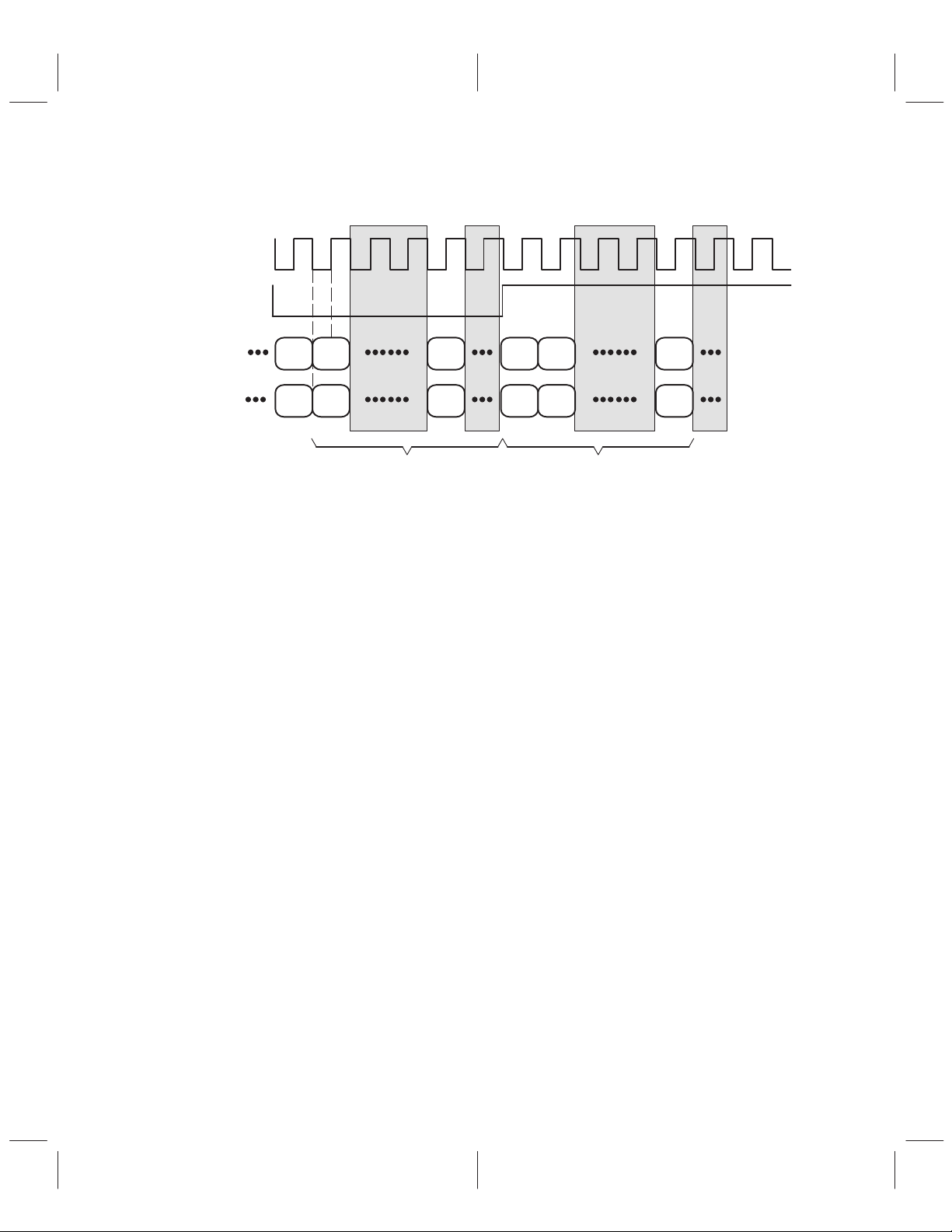
SCLK
LRCLK = f
SDOUT
SDIN
s
MSB
X
MSBX
Left Channel Right Channel
LSB
LSB
MSBX
MSBX
Figure 2–1. I2S Compatible Serial Format
2.5.2 Protocol
1. LRCLK = Sampling frequency (fs)
2. Left channel is transmitted when LR is low
3. SCLK = 64 × LRCLK. SCLK is sometimes referred to as the bit clock.
4. Serial data is sampled with the rising edge of SCLK.
5. Serial data is transmitted on the falling edge of SCLK.
6. LRCLK must have a 50% duty cycle
2.5.3 Implementation
1. LRCLK and SCLK are both inputs
2.5.4 Timing
See Figure 4–1 for I2S timing.
LSB
LSB
2–2
Page 15

2.6 Left-Justified Serial Format
SCLK
LRCLK = f
SDIN
SDOUT
s
MSB
MSB
LSB
LSB
Left Channel Right Channel
MSB
MSB
LSB
LSB
Figure 2–2. Left-Justified Serial Format
2.6.1 Protocol
1. LRCLK = Sampling frequency (fs)
2. Left channel is transmitted when LRCLK is high
3. The SDIN1 data is justified to the leading edge of the LRCLK
4. Serial data is sampled on the rising edge of SCLK
5. Serial data is transmitted on the falling edge of SCLK
6. SCLK = 32 LRCLK (32 f
SCLK is only supported for 16 bit data) or 64 LRCLK
s
7. In this mode, LRCLK does not have to be a 50% duty cycle clock. The number of bits used in the
interface sets the minimum duty cycle. There must be enough SCLK pulses to shift all of the data.
2.6.2 Implementation
1. LRCLK and SCLK are both inputs
2.6.3 Timing
See Figure 4–1 for I2S timing.
2–3
Page 16
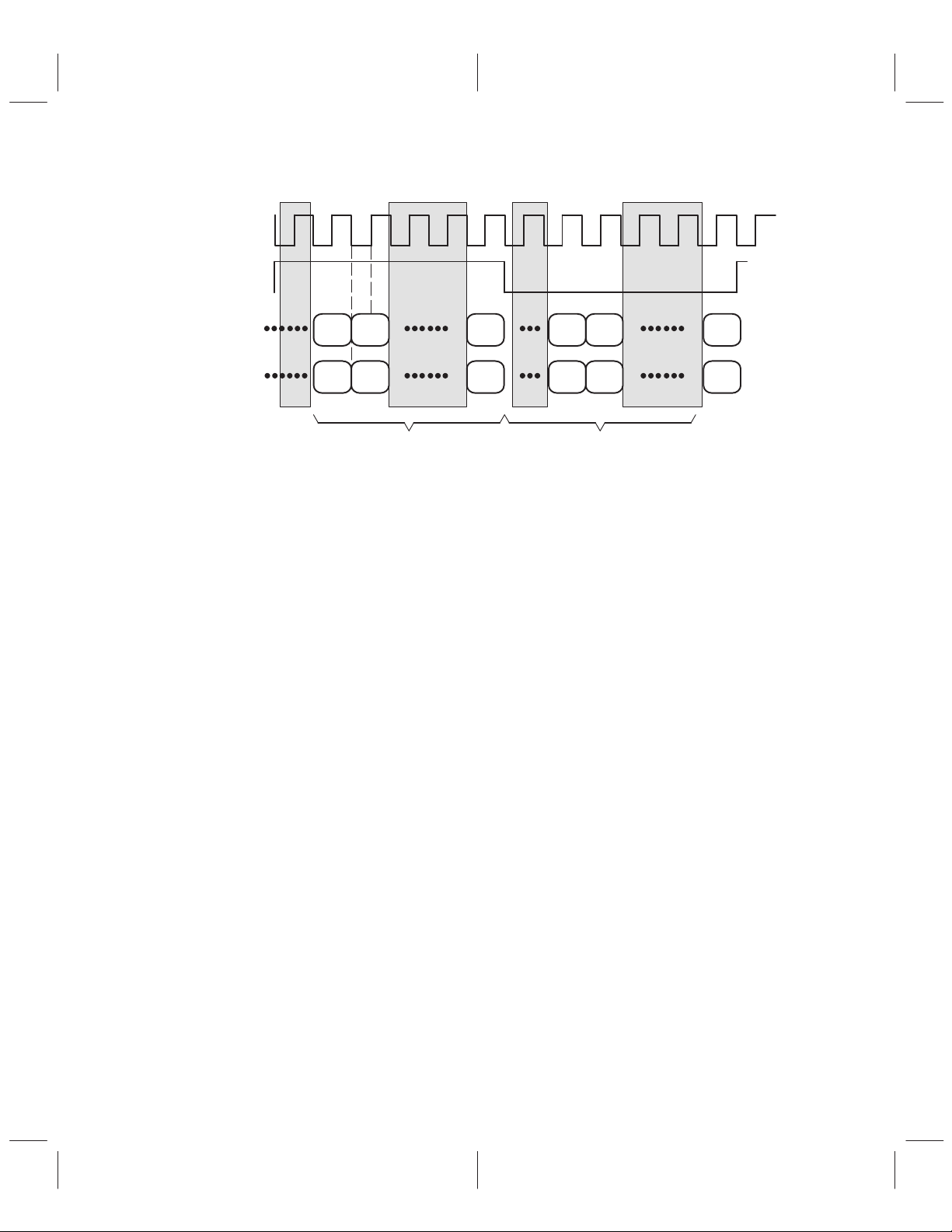
2.7 Right-Justified Serial Format
SCLK
LRCLK = f
SDIN1
SDOUT
s
MSBX
MSBX
Left Channel Right Channel
LSB
LSB
MSBX
MSBX
LSB
LSB
Figure 2–3. Right-Justified Serial Format
2.7.1 Protocol
1. LRCLK = Sampling frequency (fs)
2. Left channel is transmitted when LRCLK is high
3. The SDIN1 data is justified to the trailing edge of the LRCLK
4. Serial data is sampled on the rising edge of SCLK
5. Serial data is transmitted on the falling edge of SCLK
6. SCLK = 64 LRCLK
7. In this mode, LRCLK does not have to be a 50% duty cycle clock. The number of bits used in the
interface sets the minimum duty cycle. There must be enough SCLK pulses to shift all of the data.
2.7.2 Implementation
1. LRCLK and SCLK are both inputs
2.7.3 Timing
See Figure 4–1 for I2S timing.
2–4
Page 17

2.8 Serial Control Interface
Control parameters for the TLC320AD81C are loaded with an I2C master interface. Information is loaded
into the registers defined in appendix A,
Software Interface
(clock), to communicate between integrated circuits in a system. This device may be addressed by sending
a unique 7-bit slave address plus R/W
bit (1 byte). All compatible devices share the same pins via a
bidirectional bus using a wire-ANDed connection. A pullup resistor must be used to set the high level on the
bus. The TLC320AD81C operates in standard mode up to 100 kbps with as many devices on the bus as
desired up to the capacitance load limit of 400 pF. Additionally, the TLC320AD81C operates only in slave
mode; therefore, at least one device connected to the I
2.8.1 I2C Protocol
The bus standard uses transitions on the data pin (SDA) while the clock is high to indicate a start and stop
condition. A high-to-low transition on SDA indicates a start, and a low-to-high transition indicates a stop.
Normal data bit transitions must occur within the low time of the clock period. These conditions are shown
in Figure 2–4. These start and stop conditions for the I
generated by the master. The master must also generate the 7-bit slave address and the read/write
bit to open communication with another device and then wait for an acknowledge condition. The slave holds
the SDA bit low during the acknowledge clock period to indicate an acknowledgment. When this occurs, the
master begins transmitting. After each 8-bit word, an acknowledgment must be transmitted by the receiving
device. There is no limit on the number of bytes that may be transmitted between a start and stop condition.
When the last word has been transferred, the master must generate a stop condition to release the bus. A
generic data transfer sequence is shown in Figure 2–4.
. The I2C bus uses two pins, SDA (data) and SCL
2
C bus with this device must operate in master mode.
2
C bus are required by standard protocol to be
(R/W)
SDA
SCL
7 Bit Slave Address R/W 8 Bit Register Address (N)AA
76543210 76543210 76543210 76543210
Start Stop
8 Bit Register Data For
Address (N)
8 Bit Register Data For
A
Address (N)
A
Figure 2–4. Typical I2C Data Transfer Sequence
The definitions used by the I
2
C protocol are listed below.
Transmitter The device that sends data
Receiver The device that receives data
Master The device that initiates a transfer, generates clock signals, and terminates the
transfer
Slave The device addressed by the master
Multi-master More than one master can attempt to control the bus at the same time without
corrupting the message.
Arbitration Procedure to ensure the message is not corrupted when two masters attempt to
control the bus
Synchronization Procedure to synchronize the clock signals of two or more devices
2–5
Page 18

2.8.2 Operation
The 7-bit address for the TLC320AD81C is 01101XX, where X is a programmable address bit. Using the
CS1 and CS2 pins on the device, the two LSB address bits may be programmed. These four addresses are
2
licensed I
TLC320AD81C, the I
C addresses and will not conflict with other licensed I2C audio devices. T o communicate with the
2
C master must use 01101XX. In addition to the 7-bit device address, subaddresses
are used to direct communication to the proper memory location within the device. A complete table of
subaddresses and control registers is provided in the appendix A,
change the bass setting to 10-dB gain, section 2.8.2.1,
Write Cycle
shows how the data is written to the I2C
Software Interface
. For example, to
port:
2
T able 2–1. I
I2C ADDRESS
BYTE
0x68 01101 0 0 0
0x6A 01101 0 1 0
0x6C 01101 1 0 0
0x6E 01101 1 1 0
†
The TLC320AD81 is a write only device.
A6–A2 CS2(A1) CS1(A0) R/W
C Address Byte
†
2.8.2.1 Write Cycle
When writing to a subaddress, the correct number of data bytes must follow in order to complete the write
cycle. For example, if the volume control register with subaddress 04 (hex) is written to, six bytes of data
must follow, otherwise the cycle will be incomplete. The correct number of bytes corresponding to each
subaddress is shown in appendix A,
Start Slave Address R/W A Subaddress A Data A Stop
FUNCTION DESCRIPTION
Start Start condition as defined in I2C
Slave Address 0110100 (CS1 = CS2 = 0)
R/W 0 (write)
A Acknowledgement as defined in I2C (slave)
Sub-Address 000001 10 (see appendix A,
Data 00011100 (see appendix A,
Stop Stop condition as defined in I2C
NOTE: This table applies to serial data (SDA). Serial clock (SCL) information is not shown since the same conditions
apply as well.
Software Interface
Software Interface
Software Interface
.
)
)
2–6
Page 19
2.9 Filter Processor
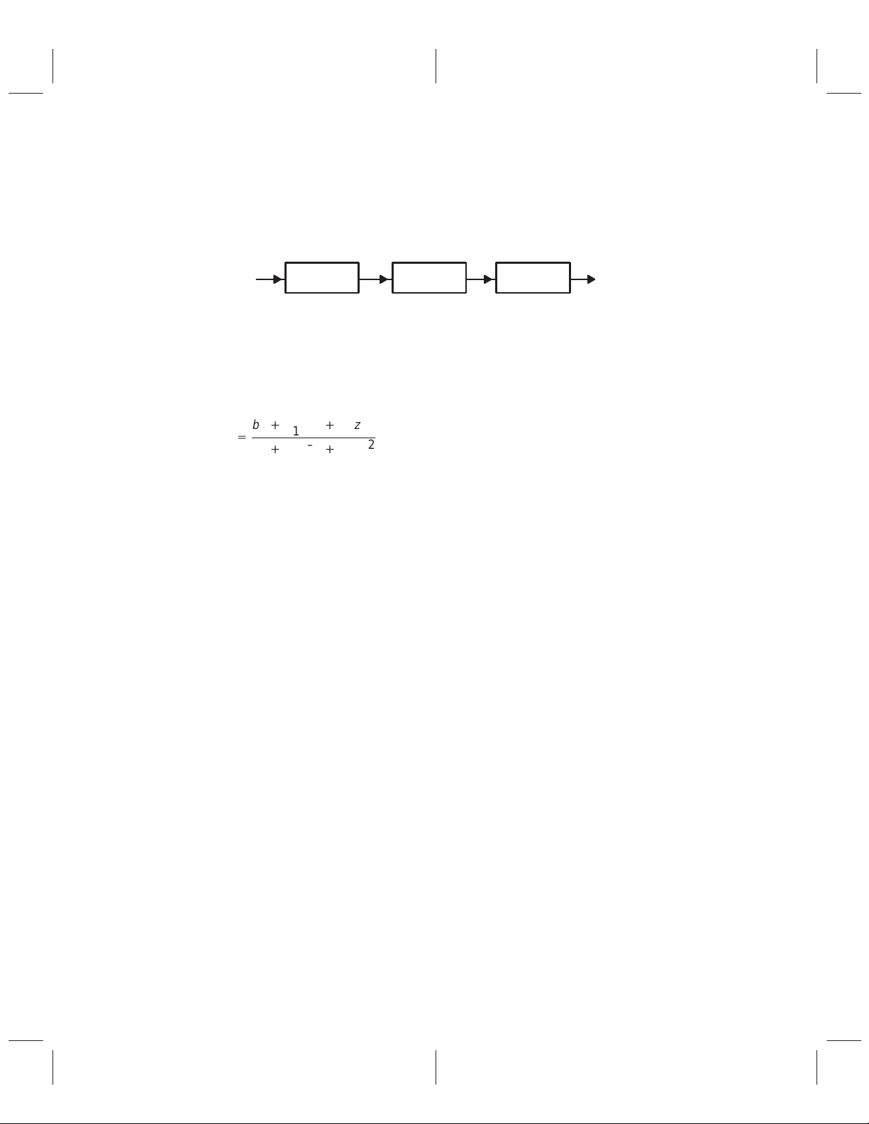
2.9.1 Biquad Block
The biquad block consists of multiple digital biquad filters per channel organized in a cascade structure as
shown in Figure 2–5. Each of these biquad filters has five downloadable 24-bit (4.20) coefficients. Each
stereo channel has independent coefficients.
Biquad 1 Biquad 2 Biquad N
Figure 2–5. Biquad Cascade Configuration
2.9.2 Filter Coefficients
The filter coefficients for the TLC320AD81C are downloaded through the I2C port and loaded into the biquad
memory space. Digital audio data coming into the device is processed by the biquad block and then
converted into analog waveforms by the DAC. Any biquad filter may be downloaded and processed by the
TLC320AD81C. The biquad structure that is used for the parametric equalization filters is as follows:
–
b1z
a1z
1
–
1
b
)
H(z
NOTE: a0 is fixed at value 1 and is not downloadable
The coefficients for these filters are quantized and represented in 4.20 format – 4 bits for the integer part
and 20 bits for the fractional part. In order to transmit them over I
coefficient into three bytes. The first nibble of byte 2 is the integer part, and the second nibble of byte 2 and
bytes 1 and 0 are the fractional parts.
0
)
+
a
)
0
)
)
b2z
a2z
–
2
–
2
2
C, it is necessary to separate each
2–7
Page 20

2.10 Volume Control Functions
The 0.5-dB steps are based on characterized data (SDOUT).
2.10.1 Soft V olume Update
The TLC320AD81C uses a soft volume update. This allows a smooth change from one volume level to the
next. The volume is represented in 4.16 format – 4 bits for the integer part and 16 bits for the fractional part.
The volume level is user adjustable (software downloadable) and has a total range of 18 dB to –70 dB plus
mute. There are 0.5-dB steps with a gain error of less than 0.12 dB over the entire range excluding mute.
Soft mute is the lowest setting (see section 2.10.2,
Interface
).
Software Soft Mute
2.10.2 Software Soft Mute
Soft mute may be implemented by inputting all 0s into the volume control register. This will cause the
TLC320AD81C to ramp the volume down to the lowest volume setting (mute) (see appendix A,
Interface
).
2.10.3 Hardware Soft Mute
Alternatively , an external hardware control pin (smute), may be used to activated soft mute. This mutes the
output of the DAC only. This has no ef fect on the volume setting for the DSP in the volume control register .
2.10.4 Mixer Control
The TLC320AD81C is capable of mixing serial audio data. The mixing is controlled through two mixer control
registers. SDIN1 and SDIN2 can be mixed with a user selectable gain for each channel. The gain control
registers are represented in 4.20 format– 4 bits for the integer part and 20 bits for the fractional part. The
gain level has a total range of 18 dB to –70 dB plus mute. There are 0.5 dB steps from 18 dB to –70 dB (see
appendix A,
control registers. The mixer controls are not intended to be dynamically updateable. Changes during
operation may cause audible artifacts.
Software Interface
). Mixer mute is implemented by inputting all 0s into the mixer 1 or mixer 2
and also see appendix A,
Software
Software
2.10.5 Treble Control
The treble gain level may be adjusted within the range of 18 dB to –18 dB with 0.5 dB step resolution. The
level changes are accomplished by downloading treble codes shown in appendix A,
section.
Software Interface
2.10.6 Bass Control
The bass gain level may be adjusted within the range of 18 dB to –18 dB with 0.5 dB step resolution. The
level changes are accomplished by downloading bass codes shown in appendix A,
Software Interface
.
2.10.7 De-Emphasis (DM)
De-emphasis is implemented in the DAC and is hardware pin controlled. De-emphasis is only valid at
44.1 kHz.
2–8
Page 21

2.11 Device Initialization
2.11.1 Reset
The reset pin allows the device to be reset. That is the TLC320AD81C returns to its default state as defined
in this section. The device does not reset automatically when power is applied to the device. A reset is
required after the following condition occurs:
1. Power is applied to any of the power pins.
Or before the following conditions occur:
1. The main control register is written to.
2. Any biquad register is written to.
2.11.2 Device Power On Plus Reset
When power is applied to the TLC320AD81C, the device will power up in an unknown state. It must be reset
before the device will be in a known state. Upon reset, the EQDAC will initialize to its default state (fast load
mode). The main control register will be configured to 1XXXXXXX, where X is don’t care, as shown in
Figure 2–7. Only the fast load bit will be set to a 1 in the main control register. This puts the device into fast
load mode (see section 2.12.1,
data will be overwritten).
Bit 7 Bit 0
1
2
The I
C address pins (CS1 and CS2) should be driven or biased to set the TLC320AD81C to a known I2C
X X X X X X X
address. This also ensures the I
Furthermore, when implementing a three or six speaker system, the CS1 and CS2 pins must always be
driven or set to unique addresses on all devices. If the DM pin is not driven, the internal bias will pull the pin
to a high logic level and de-emphasis will be on. If the SMUTE pin is not driven, the internal bias will pull the
pin to a low logic level and mute will be off. DM is not valid for any sampling frequency except 44.1 kHz. MCLK
must be driven by a 256 f
s
until the entire device has been initialized. This typically takes 5 ms for the TLC320AD81C to fully initialize
from a powered off state or all power supply pins = 0 V.
2.11.3 Fast Load
Upon entering fast load mode, the following occurs in addition to initialization:
1. All of the parametric EQ will be initialized to 0 dB (all-pass).
2. The tone (bass/treble) will be set to 0 dB.
3. The mix function will set SDIN1 to 0 dB and SDIN2 to mute (no-pass).
4. The volume will be set to mute.
While in fast load mode, it is possible to update the parametric EQ without any audio processing delay . The
audio processor will be paused while the RAM is being updated in this mode. It is recommended that
parametric EQ be downloaded in this mode. Bass and treble may not be downloaded in this mode. Mixer1
and Mixer2 registers may be downloaded in this mode or normal mode (FL bit = 0). It is not recommended
to download the volume control register and mixer registers in this mode. Once the download is complete,
the fast load bit needs to be cleared by writing a 0 into bit 7 of the main control register. This puts the
TLC320AD81C into normal mode.
When writing to the FL bit in the MCR, the audio serial format is also written to at
this time. However, the device will not recognize any serial audio until it has
returned to normal mode. Entering fast load mode only by resetting the
TLC320AD81C is recommended. Once back in normal mode, treble, bass, and
volume control may be downloaded to complete device setup.
Fast Load
). All random access memory (RAM) will be initialized (previous
Figure 2–6. Main Control Register
2
C port will be active immediately after the reset initialization phase.
clock. The I2C port will be powered up but will not acknowledge any I2C bus activity
NOTE:
2–9
Page 22

2–10
Page 23
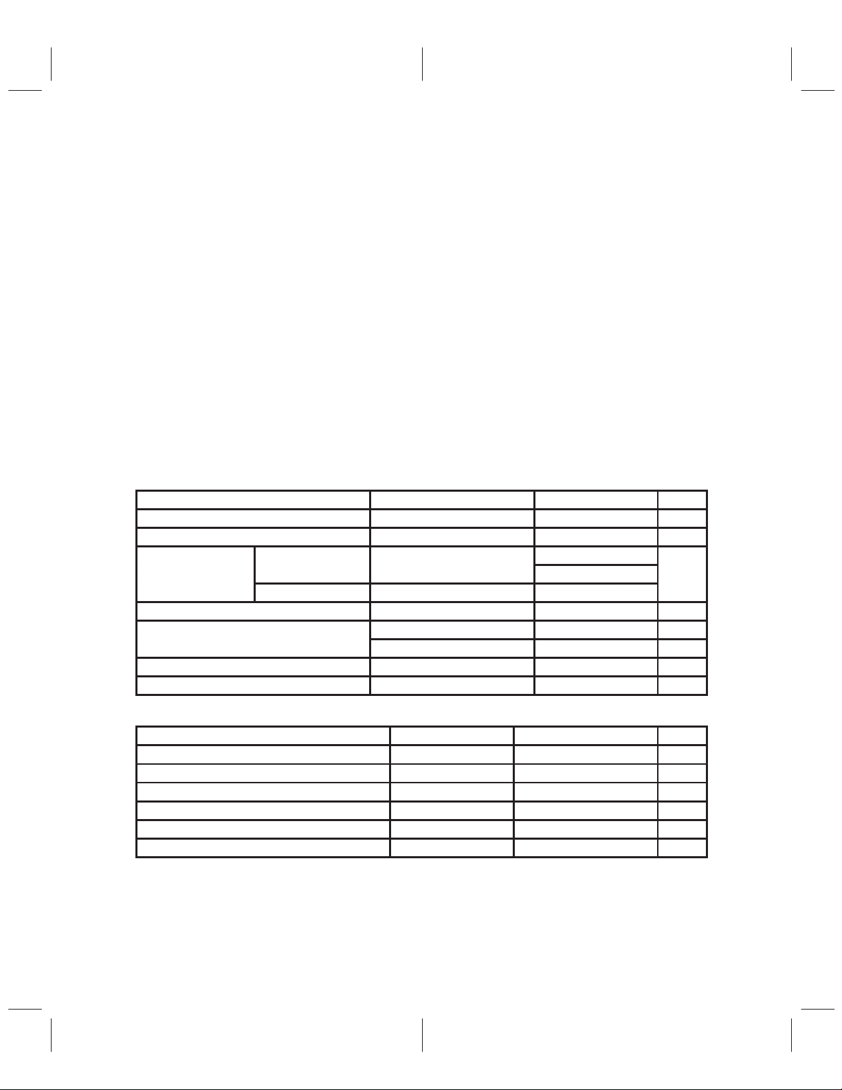
3 Specifications
AV
DAC supply current, I
3.1 Absolute Maximum Ratings Over Operating Free-air Temperature Range
(unless otherwise noted)
Supply voltage range, AVDD_PLL, DVDD –0.3 to + 5 V. . . . . . . . . . . . . . . . . . . . . . . . . . . .
Supply voltage range, AVDD_DAC, DVDD_DAC –0.3 to + 7 V. . . . . . . . . . . . . . . . . . . . . .
Digital Input voltage range –0.3 to V
Operating free-air temperature range 0°C to + 70°C. . . . . . . . . . . . . . . . . . . . . . . . . . . . . . .
Storage temperature range –65°C to + 150°C. . . . . . . . . . . . . . . . . . . . . . . . . . . . . . . . . . . .
Case temperature for 10 seconds 122.3°C. . . . . . . . . . . . . . . . . . . . . . . . . . . . . . . . . . . . . . .
Lead temperature from case for 10 seconds 97.8°C. . . . . . . . . . . . . . . . . . . . . . . . . . . . . . .
ESD tolerance
†
Stresses beyond those listed under “absolute maximum ratings” may cause permanent damage to the device. These
are stress ratings only, and functional operation of the device at these or any other conditions beyond those indicated
under “recommended operating conditions” is not implied. Exposure to absolute-maximum-rated conditions for
extended periods may affect device reliability.
‡
Human Body Model per Method 3015.2 of MIL-STD-883B.
‡
2000 V. . . . . . . . . . . . . . . . . . . . . . . . . . . . . . . . . . . . . . . . . . . . . . . . . . . . . . . .
†
+ 0.3 V. . . . . . . . . . . . . . . . . . . . . . . . . . . . . . . . . .
DD
3.2 Recommended Operating Conditions
TEST CONDITIONS MIN NOM MAX UNIT
PLL supply voltage, AV
Digital IC supply voltage, DV
DAC supply voltage
PLL and digital IC supply current, I
pp
Capacitive load for each bus line C
Operating free-air temperature, T
DD
DD
DV
DD
DD
DD
DD
L(bus)
A
VDD = 3.3 V 20 mA
AVDD = 3.6 V, DVDD = 5.5 V 15 mA
AVDD = 3.6 V, DVDD = 3.6 V 7.5 mA
SDA, SCL 400 pF
3 3.3 3.6 V
3 3.3 3.6 V
3 3.3 3.6
4.5 5 5.5
3 3.3 3.6
0 25 70 °C
V
3.3 Static Digital Specifications, TA = 0°C to 70°C, all VDD = 3.3 V ± 0.3 V
PARAMETER TEST CONDITIONS MIN TYP MAX UNIT
V
High-level input voltage 2 VDD +0.3 V
IH
V
Low-level input voltage –0.3 0.8 V
IL
V
High-level output voltage IO = –1 mA 2.4 V
OH
V
Low-level output voltage IO = 4 mA 0.4 V
OL
Input leakage current –10 10 µA
I
Output leakage current SCL, SDA –10 10 µA
lkg
DD
V
3–1
Page 24

3.4 DAC Performance Characteristics, TA = 25°C, AVDD_DAC = 5 V,
DAC signal-to-noise ratio (SNR) (see Note 2)
dB
All Other V
PARAMETER TEST CONDITIONS MIN TYP MAX UNIT
DAC resolution 16 Bits
Dynamic range 94 dB
Total harmonic distortion (THD) 0.005 0.01 %
Total harmonic distortion + noise (THD + N) –60 dB –32 dB
Crosstalk 90 dB
Frequency response 0 20 kHz
DAC conversion latency 16
OUTPUT DRIVER LEVELS
Full-scale output voltage (into 10 kΩ) AVDD_DAC = 5 V 1 Vrms
Output dc level VDD/2 V
OUTPUT DRIVER LOADING
Minimum output load impedance 2 10 kΩ
Maximum output load capacitance 100 pF
DC ACCURACY
Transition band 20 kHz
Out of band attenuation –40 dB
Interchannel gain mismatch Output drivers ±1% ±5% FSR
Potential divider resistance
Voltage at CAP VDD/2 V
NOTES: 1. All measurements done with 20-kHz low-pass filter.
2. Ratio of RMS output level with 1-kHz full-scale input, to the RMS output level with all zeros into the digital
input, measured with A-weighted filter over a 20 Hz to 20 kHz bandwidth.
= 3.3 V, fs = 44.1 kHz (see Note 1)
DD
AVDD_DAC = 5 V 90 98
AVDD_DAC = 3.3 V 90 95
AVDD_DAC = 3.3 V 0.6 Vrms
AVDD_DAC to CAP and
CAP to AVSS_DAC
Periods
80 100 120 kΩ
f
s
3–2
Page 25

3.5 Audio Serial Port Timing Requirements (see Note 3)
PARAMETER MIN TYP MAX UNIT
f
(SCLK)
t
r(SCLK)
t
f(SCLK)
t
d(SLR)
t
d(SDOUT)
t
su(SDIN)
t
h(SDIN)
†
Valid in 16-bit left justified mode only.
NOTES: 3. Timing relative to 256 fs MCLK.
Frequency, SCLK 32 f
Rise time, SCLK (see Note 4) 5 16.3 25 ns
Fall time, SCLK (see Note 4) 5 16.3 25 ns
Delay time, SCLK rising to LRCLK edge (see Note 5) 50 ns
Delay time, SDOUT valid from SCLK falling 100 ns
Setup time, SDIN before SCLK rising edge 10 ns
Hold time, SDIN from SCLK rising edge 100 ns
4. SCLK rising and falling are measured from 20% to 80%.
5. The rising edge of SCLK must not occur at the same time as either edge of LRCLK.
†
s
64 fsMHz
3.6 I2C Serial Port Timing Requirements
PARAMETER MIN MAX UNIT
f
(scl)
t
BUF
t
w(low)
t
w(high)
t
h(STA)
t
su(STA)
t
h(DAT)
t
su(DAT)
t
r
t
f
t
su(STO)
†
A device must internally provide a hold time of at least 300 ns for the SDA signal to bridge the undefined region of the
falling edge of SCL.
NOTES: 6. t
SCL clock frequency 0 100 kHz
Bus free time between start and stop 4.7 µs
Pulse duration, SCL clock low (see Note 6) 4.7 µs
Pulse duration, SCL clock high (see Note 7) 4 µs
Hold time, repeated start 4 µs
Setup time, repeated start 4.7 20 µs
Hold time, data 0
Setup time, data 250 ns
Rise time for SDA and SCL 1000 ns
Fall time for SDA and SCL 300 ns
Setup time for stop condition 4 µs
is measured from the end of tf to the beginning of t
7. t
w(low)
is measured from the end of tr to the beginning of t
w(high)
r.
f.
†
µs
3–3
Page 26

3–4
Page 27

4 Parameter Measurement Information
t
c(SCLK)
SCLK
t
r(SCLK)
SDA
SCL
t
BUF
LRCK
SDOUT
SDIN
PS
t
t
h(STA)
Data Line
d(SDOUT)
t
su(SDIN)
Valid
t
r
Stable
t
d(SLR)
Figure 4–1. I2S Timing
t
h(DAT)
t
Change of Data
Allowed
f
t
su(DAT)
t
h(SDIN)
t
su(STA)
t
d(SLR)
t
h(STA)
t
f(SCLK)
t
su(STO)
P
Figure 4–2. I2C Timing
4–1
Page 28

4–2
Page 29

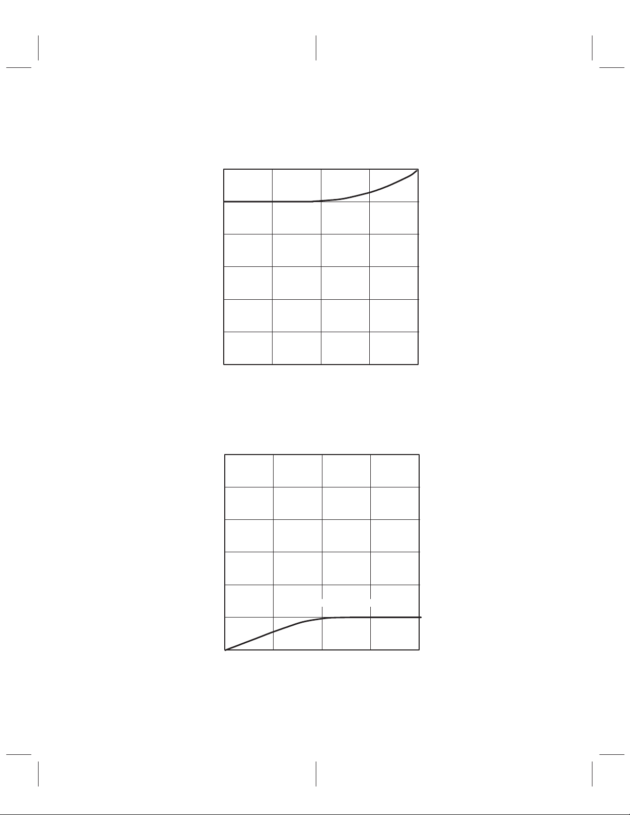
5 Typical Characteristics
At TA = 25°C, AVDD_DAC = 5 V , DVDD_DAC = 5 V , all other VDD = 3.3 V , fs = 44.1 kHz, SYSCLK = 256fs,
unless otherwise noted.
TOTAL HARMONIC DISTORTION
vs
FREE-AIR TEMPERATURE
0.009
0.008
0.007
0.006
0.005
0.004
0.003
0.002
Total Harmonic Distortion – dB
0.001
0 dB
0
025
TA – Temperature – °C
50 70
5–1
Page 30

TOTAL HARMONIC DISTORTION + NOISE
vs
FREE-AIR TEMPERATURE
38
36
34
32
30
28
26
24
Total Harmonic Distortion + Noise – dB
22
20
0255070
TA – Temperature – °C
–60 dB
5–2
Page 31

99
98
97
96
95
94
SNR – Signal-To-Noise Ratio – dB
93
SIGNAL-TO-NOISE RATIO
vs
FREE-AIR TEMPERATURE
SNR
92
025
TA – Temperature – °C
FREE-AIR TEMPERATURE
99
98
97
96
95
Dynamic Range – dB
94
93
92
025
TA – Temperature – °C
50 70
DYNAMIC RANGE
vs
Dynamic Range
50 70
5–3
Page 32

TOTAL HARMONIC DISTORTION
SUPPLY VOLTAGE
0.009
0.008
0.007
0.006
0.005
0.004
0.003
0.002
Total Harmonic Distortion – dB
0.001
vs
0 dB
0
4.5 4.75
AVDD_DAC, DVDD_DAC – Supply Voltage – V
5 5.5
TOTAL HARMONIC DISTORTION + NOISE
vs
SUPPLY VOLTAGE
38
36
34
32
30
28
26
24
Total Harmonic Distortion + Noise – dB
22
20
4.5 4.75
AVDD_DAC, DVDD_DAC – Supply Voltage – V
–60 dB
5 5.5
5.25
5.25
5–4
Page 33
99
98
97
96
95
SNR – Signal-To-Noise Ratio – dB
94
SIGNAL-TO-NOISE RATIO
vs
SUPPLY VOLTAGE
SNR
93
4.5 4.75
AVDD_DAC, DVDD_DAC – Supply Voltage – V
99
98
97
96
95
Dynamic Range – dB
94
93
4.5 4.75
AVDD_DAC, DVDD_DAC – Supply Voltage – V
5 5.5
DYNAMIC RANGE
vs
SUPPLY VOLTAGE
Dynamic Range
5 5.5
5.25
5.25
5–5
Page 34

5–6
Page 35
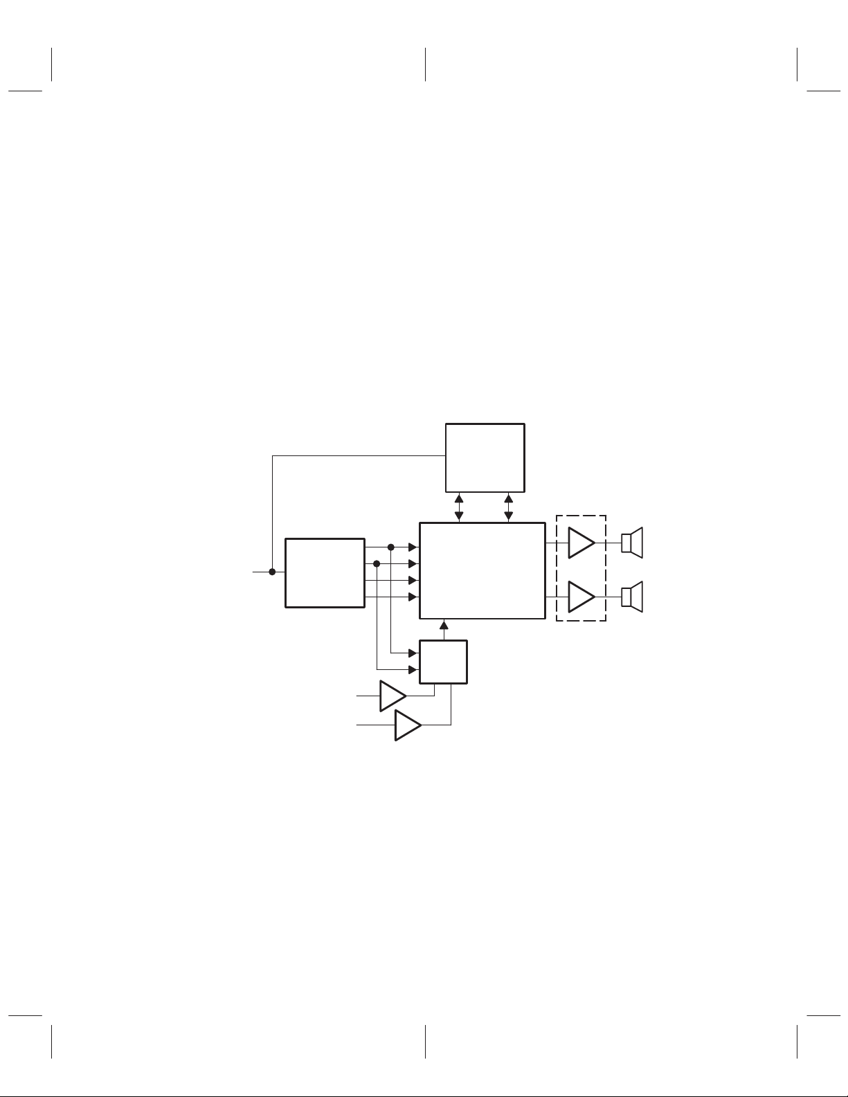
6 Application Information
Typical applications for the TLC320AD81C include:
• Digital speakers
• Multi media monitors with speakers
• USB audio devices
The TLC320AD81C is designed to interface to a serial audio source and can handle up to two SDIN audio
data streams. In a multiple SDIN application as shown, latency of the ADC should be taken into account.
A controller is used to translate between USB audio and serial audio. Audio control functions are
downloaded to the TLC320AD81C through the I
the USB controller, although shown as separate controllers. The output of the device interfaces to the power
amplifiers, however, prefiltering is recommended. Voltage regulators, and bypass capacitors (not shown)
on the power supplies are recommended good practices.
Digital Audio
I2S Data
2
C port. One option is for this to be the same controller as
USB
to
I2C
Controller
Power
Amplifier
USB Data Stream
SCL SDA
USB
to
I2S
Controller
MIC1
MIC2
MCLK
LRCLK
SDIN1
SCLK
SDIN2
ADC
TLC320AD81C
Figure 6–1. Example USB Audio System
Left
Right
6–1
Page 36

I2C
Controller
SCL SDA
SPDIF
Data
SPDIF
RECEIVER
MCLK
LRCLK
SDIN1
SCLK
TLC320AD81C
Left
Right
Figure 6–2. Example SPDIF Audio System
6.1 Audio Data
The TLC320AD81C handles three data lengths for received audio data. In 20-bit mode, the two least
significant bits are truncated to 18 bits before the data is processed. These 18 bits are available after
processing at the SDOUT pin. However, two more bits are truncated before the digital-to-analog (D/A)
conversion of the data, therefore 16-bit analog performance is seen at the analog output pins (Out_L and
Out_R). In 18-bit mode, all 18 bits are passed through or processed digitally. The 18 bits are available at
the SDOUT pin. Again two bits are truncated before the digital-to-analog conversion for 16-bit analog output
performance. In 16-bit mode, all 16 bits are passed through or processed both digitally and through D/A
conversion, but the 16 bits are shifted up two significant bit places before processing. Thus 18 bits are
available at SDOUT with 16 bits being data and the two least significant bits being padded zeros. The original
16 bits are passed through the D/A converter.
6–2
Page 37

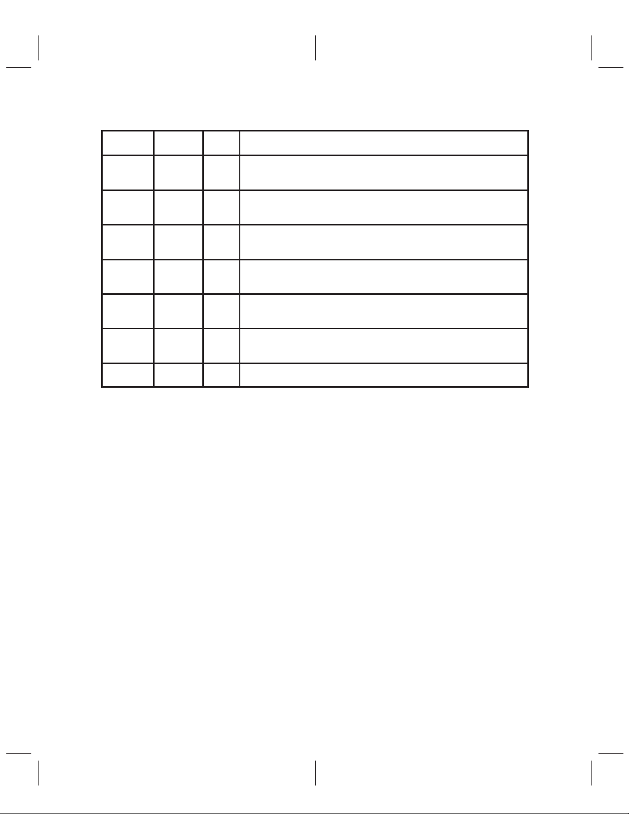
Appendix A
Software Interface
T able A–1. Register Map
REGISTER ADDRESS
Reserved 0x00
MCR 0x01 1 C(7–0)
Reserved 0x02
Reserved 0x03
†
Volume
Treble 0x05 1 T(7–0)
Bass 0x06 1 B(7–0)
‡
Mixer 1
‡
Mixer 2
Reserved 0x09
Left
Biquad 0
Left
Biquad 1
Left
Biquad 2
Left
Biquad 3
Left
Biquad 4
Left
Biquad 5
Reserved 0x10
Reserved 0x11
Reserved 0x12
†
‡
‡
‡
‡
‡
‡
The volume value is a 4.16 coefficient. In order to transmit it over I2C, it is necessary to separate the value into three
bytes. Byte 2 is the integer part and bytes 1 and 0 are the fractional parts.
The mixer gain values and biquad coefficients are 4.20 coefficients. In order to transmit them over I2C, it is necessary
to separate the value into three bytes. The first nibble of byte 2 is the integer part and the second nibble of byte 2 and
bytes 1 and 0 being the fractional parts.
0x04 6 VL(23–16), VL(15–8), VL(7–0), VR(23–16), VR(15–8), VR(7–0)
0x07 3 S(23–16), S(15–8), S(7–0)
0x08 3 S(23–16), S(15–8), S(7–0)
0x0A 15 B0(23–16), B0(15–8), B0(7–0), B1(23–16), B1(15–8), B1(7–0), B2(23–16),
0x0B 15 B0(23–16), B0(15–8), B0(7–0), B1(23–16), B1(15–8), B1(7–0), B2(23–16),
0x0C 15 B0(23–16), B0(15–8), B0(7–0), B1(23–16), B1(15–8), B1(7–0), B2(23–16),
0x0D 15 B0(23–16), B0(15–8), B0(7–0), B1(23–16), B1(15–8), B1(7–0), B2(23–16),
0x0E 15 B0(23–16), B0(15–8), B0(7–0), B1(23–16), B1(15–8), B1(7–0), B2(23–16),
0x0F 15 B0(23–16), B0(15–8), B0(7–0), B1(23–16), B1(15–8), B1(7–0), B2(23–16),
NO. of
BYTES
BYTE DESCRIPTION
B2(15–8), B2(7–0), A1(23–16), A1(15–8), A1(7–0), A2(23–16), A2(15–8),
A2(7–0)
B2(15–8), B2(7–0), A1(23–16), A1(15–8), A1(7–0), A2(23–16), A2(15–8),
A2(7–0)
B2(15–8), B2(7–0), A1(23–16), A1(15–8), A1(7–0), A2(23–16), A2(15–8),
A2(7–0)
B2(15–8), B2(7–0), A1(23–16), A1(15–8), A1(7–0), A2(23–16), A2(15–8),
A2(7–0)
B2(15–8), B2(7–0), A1(23–16), A1(15–8), A1(7–0), A2(23–16), A2(15–8),
A2(7–0)
B2(15–8), B2(7–0), A1(23–16), A1(15–8), A1(7–0) A2(23–16), A2(15–8),
A2(7–0)
A–1
Page 38
T able A–1. Register Map (Continued)
REGISTER ADDRESS
Right
Biquad 0
Right
Biquad 1
Right
Biquad 2
Right
Biquad 3
Right
Biquad 4
Right
Biquad 5
Reserved 0x19 to
†
‡
‡
‡
‡
‡
‡
‡
The volume value is a 4.16 coefficient. In order to transmit it over I2C, it is necessary to separate the value into three
bytes. Byte 2 is the integer part and bytes 1 and 0 are the fractional parts.
The mixer gain values and biquad coefficients are 4.20 coefficients. In order to transmit them over I2C, it is necessary
to separate the value into three bytes. The first nibble of byte 2 is the integer part and the second nibble of byte 2 and
bytes 1 and 0 being the fractional parts.
0x13 15 B0(23–16), B0(15–8), B0(7–0), B1(23–16), B1(15–8), B1(7–0), B2(23–16),
0x14 15 B0(23–16), B0(15–8), B0(7–0), B1(23–16), B1(15–8), B1(7–0), B2(23–16),
0x15 15 B0(23–16), B0(15–8), B0(7–0), B1(23–16), B1(15–8), B1(7–0), B2(23–16),
0x16 15 B0(23–16), B0(15–8), B0(7–0), B1(23–16), B1(15–8), B1(7–0), B2(23–16),
0x17 15 B0(23–16), B0(15–8), B0(7–0), B1(23–16), B1(15–8), B1(7–0), B2(23–16),
0x18 15 B0(23–16), B0(15–8), B0(7–0), B1(23–16), B1(15–8), B1(7–0), B2(23–16),
0xFF
NO. of
BYTES
BYTE DESCRIPTION
B2(15–8), B2(7–0), A1(23–16), A1(15–8), A1(7–0), A2(23–16), A2(15–8),
A2(7–0)
B2(15–8), B2(7–0), A1(23–16), A1(15–8), A1(7–0), A2(23–16), A2(15–8),
A2(7–0)
B2(15–8), B2(7–0), A1(23–16), A1(15–8), A1(7–0), A2(23–16), A2(15–8),
A2(7–0)
B2(15–8), B2(7–0), A1(23–16), A1(15–8), A1(7–0), A2(23–16), A2(15–8),
A2(7–0)
B2(15–8), B2(7–0), A1(23–16), A1(15–8), A1(7–0), A2(23–16), A2(15–8),
A2(7–0)
B2(15–8), B2(7–0), A1(23–16), A1(15–8), A1(7–0), A2(23–16), A2(15–8),
A2(7–0)
A–2
Page 39
Main Control Register (MCR)
The serial port for this device is flexible, making it easier to interface with many different compatible systems.
Configuration of the digital audio serial interface is set up through the main control register as shown below.
Bits F0 and F1 allow selection between three different serial data formats (right justified = 00, right
justified = 01, and I
value as the input serial port mode set by F0 and F1. Bits W0 and W1 allow selection between three different
word widths (16-bit word = 00, 18-bit word = 01, and 20-bit word = 10). The SC bit selects 32f
(1) bit clock. The FL bit is primarily for use during initialization and is defined in the device initialization
section. See section 2.8
control register.
BIT DESCRIPTOR FUNCTION VALUE FUNCTION
C(7) FL Fast load
C(6) SC SCLK frequency
C(5,4) E(1,0) Output serial port mode
C(3,2) F(1,0) Input serial port mode
C(1,0) W(1,0) Serial port word length
2
S standard = 10). The output serial port mode set by E0 and E1 must be set to the same
(0) or 64f
s
Serial Control Interface
for additional information on how to address the main
Table A–2. Main Control Register (MCR)
C7 C6 C5 C4 C3 C2 C1 C0
FL SC E1 E0 F1 F0 W1 W0
1 x x x x x x x
Table A–3. Main Control Register (MCR) Description
0 Normal operating mode
1 (default) Fast load mode
0 SCLK = 32 f
1 SCLK = 64 f
00 Left justified
01 Right justified
10 I2S
11 Reserved
00 Left justified
01 Right justified
10 I2S
11 Reserved
00 16 bit
01 18 bit
10 20 bit
11 Reserved
s
s
s
A–3
Page 40
GAIN
(dB)
18.0 07, F1, 7B
17.5 07, 7F , BB
17.0 07, 14, 57
16.5 06, AE, F6
16.0 06, 4F , 40
15.5 05, F4, E5
15.0 05, 9F , 98
14.5 05, 4F , 10
14.0 05, 03, 0A
13.5 04, BB, 44
13.0 04, 77, 83
12.5 04, 37, 8B
12.0 03, FB, 28
11.5 03, C2, 25
11.0 03, 8C, 53
10.5 03, 59, 83
10.0 03, 29, 8B
VOLUME
V(23–16),
V(15–8),
V(7–0)
9.5 02, FC, 42
9.0 02, D1, 82
8.5 02, A9, 25
8.0 02, 83, 0B
7.5 02, 5F, 12
7.0 02, 3D, 1D
6.5 02, 1D, 0E
6.0 01, FE, CA
5.5 01, E2, 37
5.0 01, C7, 3D
4.5 01, AD, C6
4.0 01, 95, BC
3.5 01, 7F, 09
3.0 01, 69, 9C
2.5 01, 55, 62
2.0 01, 42, 49
1.5 01, 30, 42
1.0 01, 1F, 3D
0.5 01, 0F, 2B
Table A–4. Volume Gain Values
[The gain error is less than 0.12 dB (excluding mute)]
GAIN
(dB)
–0.5 00, F1, AE
–1.0 00, E4, 29
–1.5 00, D7, 66
–2.0 00, CB, 59
–2.5 00, BF , F9
–3.0 00, B5, 3C
–3.5 00, AB, 19
–4.0 00, A1, 86
–4.5 00, 98, 7D
–5.0 00, 8F , F6
–5.5 00, 87, E8
–6.0 00, 80, 4E
–6.5 00, 79, 20
–7.0 00, 72, 5A
–7.5 00, 6B, F4
–8.0 00, 65, EA
–8.5 00, 60, 37
–9.0 00, 5A, D5
–9.5 00, 55, C0
–10.0 00, 50, F4
–10.5 00, 4C, 6D
–11.0 00, 48, 27
–11.5 00, 44, 1D
–12.0 00, 40, 4E
–12.5 00, 3C, B5
–13.0 00, 39, 50
–13.5 00, 36, 1B
–14.0 00, 33, 14
–14.5 00, 30, 39
–15.0 00, 2D, 86
–15.5 00, 2A, FA
–16.0 00, 28, 93
–16.5 00, 26, 4E
–17.0 00, 24, 29
–17.5 00, 22, 23
–18.0 00, 20, 3A
VOLUME
V(23–16),
V(15–8),
V(7–0)
0.0 01, 00, 00
GAIN
(dB)
–18.5 00, 1E, 6D
–19.0 00, 1C, B9
–19.5 00, 1B, 1E
–20.0 00, 19, 9A
–20.5 00, 18, 2B
–21.0 00, 16, D1
–21.5 00, 15, 8A
–22.0 00, 14, 56
–22.5 00, 13, 33
–23.0 00, 12, 20
–23.5 00, 11, 1C
–24.0 00, 10, 27
–24.5 00, 0F, 40
–25.0 00, 0E, 65
–25.5 00, 0D, 97
–26.0 00, 0C, D5
–26.5 00, 0C, 1D
–27.0 00, 0B, 6F
–27.5 00, 0A, CC
–28.0 00, 0A, 31
–28.5 00, 09, 9F
–29.0 00, 09, 15
–29.5 00, 08, 93
–30.0 00, 08, 18
–30.5 00, 07, A5
–31.0 00, 07, 37
–31.5 00, 06, D0
–32.0 00, 06, 6E
–32.5 00, 06, 12
–33.0 00, 05, BB
–33.5 00, 05, 69
–34.0 00, 05, 1C
–34.5 00, 04, D2
–35.0 00, 04, 8D
–35.5 00, 04, 4C
–36.0 00, 04, 0F
–36.5 00, 03, D5
VOLUME
V(23–16),
V(15–8),
V(7–0)
GAIN
(dB)
–37.0 00, 03, 9E
–37.5 00, 03, 6A
–38.0 00, 03, 39
–38.5 00, 03, 0B
–39.0 00, 02, DF
–39.5 00, 02, B6
–40.0 00, 02, 8F
–40.5 00, 02, 6B
–41.0 00, 02, 48
–41.5 00, 02, 27
–42.0 00, 02, 09
–42.5 00, 01, EB
–43.0 00, 01, D0
–43.5 00, 01, B6
–44.0 00, 01, 9E
–44.5 00, 01, 86
–45.0 00, 01, 71
–45.5 00, 01, 5C
–46.0 00, 01, 48
–46.5 00, 01, 36
–47.0 00, 01, 25
–47.5 00, 01, 14
–48.0 00, 01, 05
–48.5 00, 00, F6
–49.0 00, 00, E9
–49.5 00, 00, DC
–50.0 00, 00, CF
–50.5 00, 00, C4
–51.0 00, 00, B9
–51.5 00, 00, AE
–52.0 00, 00, A5
–52.5 00, 00, 9B
–53.0 00, 00, 93
–53.5 00, 00, 8B
–54.0 00, 00, 83
–54.5 00, 00, 7B
–55.0 00, 00, 75
VOLUME
V(23–16),
V(15–8),
V(7–0)
A–4
Page 41

GAIN
(dB)
–55.5 00, 00, 6E
–56.0 00, 00, 68
–56.5 00, 00, 62
–57.0 00, 00, 5D
–57.5 00, 00, 57
–58.0 00, 00, 53
–58.5 00, 00, 4E
–59.0 00, 00, 4A
VOLUME
V(23–16),
V(15–8),
V(7–0)
(Both left and right channel will be given the same treble gain setting)
Gain
(dB)
18.0 0x01
17.5 0x09
17.0 0x10
16.5 0x16
16.0 0x1C
15.5 0x22
15.0 0x28
14.5 0x2D
14.0 0x32
13.5 0x36
13.0 0x3A
12.5 0x3E
12.0 0x42
11.5 0x45
11.0 0x49
10.5 0x4C
10.0 0x4F
9.5 0x52
9.0 0x55
T(7–0)
(hex)
T able A–4. Volume Gain Values
[The gain error is less than 0.12 dB (excuding mute)] (Continued)
GAIN
(dB)
–59.5 00, 00, 45
–60.0 00, 00, 42
–60.5 00, 00, 3E
–61.0 00, 00, 3A
–61.5 00, 00, 37
–62.0 00, 00, 34
–62.5 00, 00, 31
–63.0 00, 00, 2E
VOLUME
V(23–16),
V(15–8),
V(7–0)
GAIN
(dB)
–63.5 00, 00, 2C
–64.0 00, 00, 29
–64.5 00, 00, 27
–65.0 00, 00, 25
–65.5 00, 00, 23
–66.0 00, 00, 21
–66.5 00, 00, 1F
–67.0 00, 00, 1D
VOLUME
V(23–16),
V(15–8),
V(7–0)
GAIN
(dB)
–67.5 00, 00, 1C
–68.0 00, 00, 1A
–68.5 00, 00, 19
–69.0 00, 00, 17
–69.5 00, 00, 16
–70.0 00, 00, 15
Mute 00, 00, 00
Table A–5. Treble Control Register
Gain
(dB)
8.5 0x57
8.0 0x5A
7.5 0x5C
7.0 0x5E
6.5 0x60
6.0 0x62
5.5 0x63
5.0 0x65
4.5 0x66
4.0 0x68
3.5 0x69
3.0 0x6B
2.5 0x6C
2.0 0x6D
1.5 0x6E
1.0 0x70
0.5 0x71
0.0 0x72
T(7–0)
(hex)
Gain
(dB)
–0.5 0x73
–1.0 0x74
–1.5 0x75
–2.0 0x76
–2.5 0x77
–3.0 0x78
–3.5 0x79
–4.0 0x7A
–4.5 0x7B
–5.0 0x7C
–5.5 0x7D
–6.0 0x7E
–6.5 0x7F
–7.0 0x80
–7.5 0x81
–8.0 0x82
–8.5 0x83
–9.0 0x84
–9.5 0x85
T(7–0)
(hex)
Gain
(dB)
–10.0 0x86
–10.5 0x87
–11.0 0x88
–11.5 0x89
–12.0 0x8A
–12.5 0x8B
–13.0 0x8C
–13.5 0x8D
–14.0 0x8E
–14.5 0x8F
–15.0 0x90
–15.5 0x91
–16.0 0x92
–16.5 0x93
–17.0 0x94
–17.5 0x95
–18.0 0x96
VOLUME
V(23–16),
V(15–8),
V(7–0)
T(7–0)
(hex)
A–5
Page 42
Gain
(dB)
18.0 0x01
17.5 0x03
17.0 0x06
16.5 0x08
16.0 0x0A
15.5 0x0B
15.0 0x0D
14.5 0x0F
14.0 0x10
13.5 0x12
13.0 0x13
12.5 0x14
12.0 0x16
11.5 0x17
11.0 0x18
10.5 0x19
10.0 0x1C
9.5 0x1F
9.0 0x21
B(7–0)
(hex)
Table A–6. Bass Control Register
(Both left and right channel will be given the same bass setting)
Gain
(dB)
8.5 0x23
8.0 0x25
7.5 0x26
7.0 0x28
6.5 0x29
6.0 0x2B
5.5 0x2C
5.0 0x2E
4.5 0x30
4.0 0x31
3.5 0x33
3.0 0x35
2.5 0x36
2.0 0x38
1.5 0x39
1.0 0x3B
0.5 0x3C
0.0 0x3E
B(7–0)
(hex)
Gain
(dB)
–0.5 0x40
–1.0 0x42
–1.5 0x44
–2.0 0x46
–2.5 0x49
–3.0 0x4B
–3.5 0x4D
–4.0 0x4F
–4.5 0x51
–5.0 0x53
–5.5 0x54
–6.0 0x55
–6.5 0x56
–7.0 0x58
–7.5 0x59
–8.0 0x5A
–8.5 0x5C
–9.0 0x5D
B(7–0)
(hex)
Gain
(dB)
–9.5 0x5F
–10.0 0x61
–10.5 0x64
–11.0 0x66
–11.5 0x69
–12.0 0x6B
–12.5 0x6D
–13.0 0x6E
–13.5 0x70
–14.0 0x72
–14.5 0x74
–15.0 0x76
–15.5 0x78
–16.0 0x7A
–16.5 0x7D
–17.0 0x7F
–17.5 0x82
–18.0 0x86
B(7–0)
(hex)
Gain
(dB)
18.0 7F, 17, AF
17.5 77, FB, AA
17.0 71, 45, 75
16.5 6A, EF, 5D
16.0 64, F4, 03
15.5 5F, 4E, 52
15.0 59, F9, 80
14.5 54, F1, 06
14.0 50, 30, A1
13.5 4B, B4, 46
13.0 47, 78, 28
12.5 43, 78, B0
12.0 3F, B2, 78
11.5 3C, 22, 4C
A–6
S(23–16),
S(15–8),
S(7–0)
Gain
T able A–7. Mixer1 and Mixer2 Gain Values
[The gain error is less than 0.12 dB (excluding mute)]
Gain
(dB)
11.0 38, C5, 28
10.5 35, 98, 2F
10.0 32, 98, B0
9.5 2F, C4, 20
9.0 2D, 18, 18
8.5 2A, 92, 54
8.0 28, 30, AF
7.5 25, F1, 25
7.0 23, D1, CD
6.5 21, D0, D9
6.0 1F, EC, 98
5.5 1E, 23, 6D
5.0 1C, 73, D5
4.5 1A, DC, 61
Gain
S(23–16),
S(15–8),
S(7–0)
Gain
(dB)
4.0 19, 5B, B8
3.5 17, F0, 94
3.0 16, 99, C0
2.5 15, 56, 1A
2.0 14, 24, 8E
1.5 13, 04, 1A
1.0 11, F3, C9
0.5 10, F2, B4
0.0 10, 00, 00
–0.5 0F, 1A, DF
–1.0 0E, 42, 90
–1.5 0D, 76, 5A
–2.0 0C, B5, 91
–2.5 0B, FF, 91
Gain
S(23–16),
S(15–8),
S(7–0)
Gain
(dB)
–3.0 0B, 53, BE
–3.5 0A, B1, 89
–4.0 0A, 18, 66
–4.5 09, 87, D5
–5.0 08, FF, 59
–5.5 08, 7E, 80
–6.0 08, 04, DC
–6.5 07, 92, 07
–7.0 07, 25, 9D
–7.5 06, BF, 44
–8.0 06, 5E, A5
–8.5 06, 03, 6E
–9.0 05, AD, 50
–9.5 05, 5C, 04
Gain
S(23–16),
S(15–8),
S(7–0)
Page 43

[The gain error is less than 0.12 dB (excluding mute)] (Continued)
Gain
(dB)
–10.0 05, 0F, 44
–10.5 04, C6, D0
–11.0 04, 82, 68
–11.5 04, 41, D5
–12.0 04, 04, DE
–12.5 03, CB, 50
–13.0 03, 94, FA
–13.5 03, 61, AF
–14.0 03, 31, 42
–14.5 03, 03, 8A
–15.0 02, D8, 62
–15.5 02, AF, A3
–16.0 02, 89, 2C
–16.5 02, 64, DB
–17.0 02, 42, 93
–17.5 02, 22, 35
–18.0 02, 03, A7
–18.5 01, E6, CF
–19.0 01, CB, 94
–19.5 01, B1, DE
–20.0 01, 99, 99
–20.5 01, 82, AF
–21.0 01, 6D, 0E
–21.5 01, 58, A2
–22.0 01, 45, 5B
–22.5 01, 33, 28
–23.0 01, 21, F9
–23.5 01, 11, C0
–24.0 01, 02, 70
–24.5 00, F3, FB
Gain
S(23–16),
S(15–8),
S(7–0)
T able A–7. Example Mixer1 and Mixer2 Gain Values
Gain
(dB)
–25.0 00, E6, 55
–25.5 00, D9, 73
–26.0 00, CD, 49
–26.5 00, C1, CD
–27.0 00, B6, F6
–27.5 00, AC, BA
–28.0 00, A3, 10
–28.5 00, 99, F1
–29.0 00, 91, 54
–29.5 00, 89, 33
–30.0 00, 81, 86
–30.5 00, 7A, 48
–31.0 00, 73, 70
–31.5 00, 6C, FB
–32.0 00, 66, E3
–32.5 00, 61, 21
–33.0 00, 5B, B2
–33.5 00, 56, 91
–34.0 00, 51, B9
–34.5 00, 4D, 27
–35.0 00, 48, D6
–35.5 00, 44, C3
–36.0 00, 40, EA
–36.5 00, 3D, 49
–37.0 00, 39, DB
–37.5 00, 36, 9E
–38.0 00, 33, 90
–38.5 00, 30, AE
–39.0 00, 2D, F5
–39.5 00, 2B, 63
Gain
S(23–16),
S(15–8),
S(7–0)
Gain
(dB)
–40.0 00, 28, F5
–40.5 00, 26, AB
–41.0 00, 24, 81
–41.5 00, 22, 76
–42.0 00, 20, 89
–42.5 00, 1E, B7
–43.0 00, 1C, FF
–43.5 00, 1B, 60
–44.0 00, 19, D8
–44.5 00, 18, 65
–45.0 00, 17, 08
–45.5 00, 15, BE
–46.0 00, 14, 87
–46.5 00, 13, 61
–47.0 00, 12, 4B
–47.5 00, 11, 45
–48.0 00, 10, 4E
–48.5 00, 0F, 64
–49.0 00, 0E, 88
–49.5 00, 0D, B8
–50.0 00, 0C, F3
–50.5 00, 0C, 3A
–51.0 00, 0B, 8B
–51.5 00, 0A, E5
–52.0 00, 0A, 49
–52.5 00, 09, B6
–53.0 00, 09, 2B
–53.5 00, 08, A8
–54.0 00, 08, 2C
–54.5 00, 07, B7
–55.0 00, 07, 48
Gain
S(23–16),
S(15–8),
S(7–0)
Gain
(dB)
–55.5 00, 06, E0
–56.0 00, 06, 7D
–56.5 00, 06, 20
–57.0 00, 05, C9
–57.5 00, 05, 76
–58.0 00, 05, 28
–58.5 00, 04, DE
–59.0 00, 04, 98
–59.5 00, 04, 56
–60.0 00, 04, 18
–60.5 00, 03, DD
–61.0 00, 03, A6
–61.5 00, 03, 72
–62.0 00, 03, 40
–62.5 00, 03, 12
–63.0 00, 02, E6
–63.5 00, 02, BC
–64.0 00, 02, 95
–64.5 00, 02, 70
–65.0 00, 02, 4D
–65.5 00, 02, 2C
–66.0 00, 02, 0D
–66.5 00, 01, F0
–67.0 00, 01, D4
–67.5 00, 01, BA
–68.0 00, 01, A1
–68.5 00, 01, 8A
–69.0 00, 01, 74
–69.5 00, 01, 5F
–70.0 00, 01, 4B
Mute 00, 00, 00
Gain
S(23–16),
S(15–8),
S(7–0)
A–7
Page 44

A–8
Page 45
Appendix B
Mechanical Data
DBT (R-PDSO-G**) PLASTIC SMALL-OUTLINE PACKAGE
30 PIN SHOWN
0,50
30
1
1,20 MAX
0,27
0,17
16
4,50
4,30
15
A
0,15
0,05
PINS **
DIM
A MAX
7,90
M
0,08
6,60
6,20
Seating Plane
0,10
30
28
7,90
0,15 NOM
Gage Plane
0°–8°
38
44
9,80 11,10
0,25
0,75
0,50
50
12,60
A MIN
NOTES: A. All linear dimensions are in millimeters.
B. This drawing is subject to change without notice.
C. Body dimensions do not include mold flash or protrusion, not to exceed 0,15.
D. Falls within JEDEC MO-153
7,70
7,70
12,409,60 10,90
4073252/C 10/97
B–1
Page 46

B–2
Page 47

IMPORTANT NOTICE
T exas Instruments and its subsidiaries (TI) reserve the right to make changes to their products or to discontinue
any product or service without notice, and advise customers to obtain the latest version of relevant information
to verify, before placing orders, that information being relied on is current and complete. All products are sold
subject to the terms and conditions of sale supplied at the time of order acknowledgement, including those
pertaining to warranty, patent infringement, and limitation of liability.
TI warrants performance of its semiconductor products to the specifications applicable at the time of sale in
accordance with TI’s standard warranty. Testing and other quality control techniques are utilized to the extent
TI deems necessary to support this warranty . Specific testing of all parameters of each device is not necessarily
performed, except those mandated by government requirements.
CERTAIN APPLICATIONS USING SEMICONDUCTOR PRODUCTS MAY INVOLVE POTENTIAL RISKS OF
DEATH, PERSONAL INJURY, OR SEVERE PROPERTY OR ENVIRONMENTAL DAMAGE (“CRITICAL
APPLICATIONS”). TI SEMICONDUCTOR PRODUCTS ARE NOT DESIGNED, AUTHORIZED, OR
WARRANTED TO BE SUITABLE FOR USE IN LIFE-SUPPORT DEVICES OR SYSTEMS OR OTHER
CRITICAL APPLICA TIONS. INCLUSION OF TI PRODUCTS IN SUCH APPLICATIONS IS UNDERST OOD TO
BE FULLY AT THE CUSTOMER’S RISK.
In order to minimize risks associated with the customer’s applications, adequate design and operating
safeguards must be provided by the customer to minimize inherent or procedural hazards.
TI assumes no liability for applications assistance or customer product design. TI does not warrant or represent
that any license, either express or implied, is granted under any patent right, copyright, mask work right, or other
intellectual property right of TI covering or relating to any combination, machine, or process in which such
semiconductor products or services might be or are used. TI’s publication of information regarding any third
party’s products or services does not constitute TI’s approval, warranty or endorsement thereof.
Copyright 1999, Texas Instruments Incorporated
 Loading...