

TLC320AD77C
24ĆBit 96 kHz Stereo Audio Codec
Data Manual
1999 Mixed Signal Linear Products

Printed in U.S.A.
08/99
SLAS194

TLC320AD77C
24-Bit 96 kHz Stereo Audio Codec
Data Manual
SLAS194
August1999
Printed on Recycled Paper

IMPORTANT NOTICE
T exas Instruments and its subsidiaries (TI) reserve the right to make changes to their products or to discontinue
any product or service without notice, and advise customers to obtain the latest version of relevant information
to verify, before placing orders, that information being relied on is current and complete. All products are sold
subject to the terms and conditions of sale supplied at the time of order acknowledgement, including those
pertaining to warranty, patent infringement, and limitation of liability.
TI warrants performance of its semiconductor products to the specifications applicable at the time of sale in
accordance with TI’s standard warranty. Testing and other quality control techniques are utilized to the extent
TI deems necessary to support this warranty . Specific testing of all parameters of each device is not necessarily
performed, except those mandated by government requirements.
CERTAIN APPLICATIONS USING SEMICONDUCTOR PRODUCTS MAY INVOLVE POTENTIAL RISKS OF
DEATH, PERSONAL INJURY, OR SEVERE PROPERTY OR ENVIRONMENTAL DAMAGE (“CRITICAL
APPLICATIONS”). TI SEMICONDUCTOR PRODUCTS ARE NOT DESIGNED, AUTHORIZED, OR
WARRANTED TO BE SUITABLE FOR USE IN LIFE-SUPPORT DEVICES OR SYSTEMS OR OTHER
CRITICAL APPLICA TIONS. INCLUSION OF TI PRODUCTS IN SUCH APPLICATIONS IS UNDERST OOD TO
BE FULLY AT THE CUSTOMER’S RISK.
In order to minimize risks associated with the customer’s applications, adequate design and operating
safeguards must be provided by the customer to minimize inherent or procedural hazards.
TI assumes no liability for applications assistance or customer product design. TI does not warrant or represent
that any license, either express or implied, is granted under any patent right, copyright, mask work right, or other
intellectual property right of TI covering or relating to any combination, machine, or process in which such
semiconductor products or services might be or are used. TI’s publication of information regarding any third
party’s products or services does not constitute TI’s approval, warranty or endorsement thereof.
Copyright 1999, Texas Instruments Incorporated

Contents
Section Title Page
1 Introduction 1–1. . . . . . . . . . . . . . . . . . . . . . . . . . . . . . . . . . . . . . . . . . . . . . . . . . . . . . . . . . . . . . .
1.1 Features 1–1. . . . . . . . . . . . . . . . . . . . . . . . . . . . . . . . . . . . . . . . . . . . . . . . . . . . . . . . . . . . . .
1.2 Functional Block Diagram 1–2. . . . . . . . . . . . . . . . . . . . . . . . . . . . . . . . . . . . . . . . . . . . . . .
1.3 Terminal Assignments 1–3. . . . . . . . . . . . . . . . . . . . . . . . . . . . . . . . . . . . . . . . . . . . . . . . . .
1.4 Ordering Information 1–3. . . . . . . . . . . . . . . . . . . . . . . . . . . . . . . . . . . . . . . . . . . . . . . . . . .
1.5 Terminal Functions 1–4. . . . . . . . . . . . . . . . . . . . . . . . . . . . . . . . . . . . . . . . . . . . . . . . . . . . .
2 Functional Description 2–1. . . . . . . . . . . . . . . . . . . . . . . . . . . . . . . . . . . . . . . . . . . . . . . . . . . . .
2.1 ADC Channel 2–1. . . . . . . . . . . . . . . . . . . . . . . . . . . . . . . . . . . . . . . . . . . . . . . . . . . . . . . . .
2.2 DAC Channel 2–1. . . . . . . . . . . . . . . . . . . . . . . . . . . . . . . . . . . . . . . . . . . . . . . . . . . . . . . . .
2.3 Serial Interface 2–1. . . . . . . . . . . . . . . . . . . . . . . . . . . . . . . . . . . . . . . . . . . . . . . . . . . . . . . .
2.4 Sampling Frequency 2–1. . . . . . . . . . . . . . . . . . . . . . . . . . . . . . . . . . . . . . . . . . . . . . . . . . .
2.5 Speed Mode Options 2–1. . . . . . . . . . . . . . . . . . . . . . . . . . . . . . . . . . . . . . . . . . . . . . . . . . .
2.6 Voltage Reference 2–1. . . . . . . . . . . . . . . . . . . . . . . . . . . . . . . . . . . . . . . . . . . . . . . . . . . . .
2.7 ADC Analog Input 2–2. . . . . . . . . . . . . . . . . . . . . . . . . . . . . . . . . . . . . . . . . . . . . . . . . . . . . .
2.8 DAC Analog Output 2–2. . . . . . . . . . . . . . . . . . . . . . . . . . . . . . . . . . . . . . . . . . . . . . . . . . . .
2.9 Sigma-Delta ADC 2–2. . . . . . . . . . . . . . . . . . . . . . . . . . . . . . . . . . . . . . . . . . . . . . . . . . . . . .
2.10 Decimation Filter 2–2. . . . . . . . . . . . . . . . . . . . . . . . . . . . . . . . . . . . . . . . . . . . . . . . . . . . . . .
2.11 Sigma-Delta DAC 2–2. . . . . . . . . . . . . . . . . . . . . . . . . . . . . . . . . . . . . . . . . . . . . . . . . . . . . .
2.12 Interpolation Filter 2–2. . . . . . . . . . . . . . . . . . . . . . . . . . . . . . . . . . . . . . . . . . . . . . . . . . . . . .
2.13 De-emphasis 2–2. . . . . . . . . . . . . . . . . . . . . . . . . . . . . . . . . . . . . . . . . . . . . . . . . . . . . . . . . .
2.14 Serial Interface Formats 2–2. . . . . . . . . . . . . . . . . . . . . . . . . . . . . . . . . . . . . . . . . . . . . . . .
2.14.1 MSB First Right/Left Justified Format 2–3. . . . . . . . . . . . . . . . . . . . . . . . . . . . . .
2.14.2 IIS-Compatible Serial Format 2–4. . . . . . . . . . . . . . . . . . . . . . . . . . . . . . . . . . . . .
2.14.3 MSB Left Justified Serial Interface Format 2–4. . . . . . . . . . . . . . . . . . . . . . . . .
2.14.4 DSP Compatible Serial Interface Format 2–5. . . . . . . . . . . . . . . . . . . . . . . . . . .
2.15 Sampling Frequency Ranges 2–5. . . . . . . . . . . . . . . . . . . . . . . . . . . . . . . . . . . . . . . . . . . .
2.16 Power Sequences 2–5. . . . . . . . . . . . . . . . . . . . . . . . . . . . . . . . . . . . . . . . . . . . . . . . . . . . .
2.16.1 Initial Power Up 2–5. . . . . . . . . . . . . . . . . . . . . . . . . . . . . . . . . . . . . . . . . . . . . . . .
2.16.2 Power Down/Reset 2–6. . . . . . . . . . . . . . . . . . . . . . . . . . . . . . . . . . . . . . . . . . . . .
2.16.3 Reinitialization Sequence 2–6. . . . . . . . . . . . . . . . . . . . . . . . . . . . . . . . . . . . . . . .
2.17 DAC De-Emphasis Filter 2–6. . . . . . . . . . . . . . . . . . . . . . . . . . . . . . . . . . . . . . . . . . . . . . . .
2.17.1 De-Emphasis Selection 2–6. . . . . . . . . . . . . . . . . . . . . . . . . . . . . . . . . . . . . . . . . . .
3 Specifications 3–1. . . . . . . . . . . . . . . . . . . . . . . . . . . . . . . . . . . . . . . . . . . . . . . . . . . . . . . . . . . . .
3.1 Absolute Maximum Ratings Over Operating Free-Air Temperature Range 3–1. . . . .
3.2 Recommended Operating Conditions, T
AVDD = DVDD = 3.3 V ± 10%, fs = 44.1 kHz 3–1. . . . . . . . . . . . . . . . . . . . . . . . . . . . . . .
3.3 Electrical Characteristics, TA = 25°C, AVDD = DVDD = 3.3 V ± 10%,
fs = 44.1 kHz 3–1. . . . . . . . . . . . . . . . . . . . . . . . . . . . . . . . . . . . . . . . . . . . . . . . . . . . . . . . . .
3.3.1 Static Digital Specifications, T
AVDD = DVDD = 3.3 V ± 10% 3–1. . . . . . . . . . . . . . . . . . . . . . . . . . . . . . . . . . . .
= 25°C,
A
= 25°C,
A
iii

3.3.2 ADC Digital Filter, TA = 25°C, AVDD = DVDD = 3.3 V ± 10%,
fs = 44.1 kHz 3–2. . . . . . . . . . . . . . . . . . . . . . . . . . . . . . . . . . . . . . . . . . . . . . . . . . .
3.3.3 Analog-to-Digital Converter,
T
= 25°C, AVDD = DVDD = 3.3 V, fs = 44.1 kHz 3–2. . . . . . . . . . . . . . . . . . . .
3.3.4 DAC Interpolation Filter, TA = 25°C, AVDD = DVDD = 3.3 V + 10%,
3.3.5 Digital-to-Analog Converter, TA = 25°C, AVDD = 3.3 V, fs = 44.1 kHz,
3.3.6 Output Performance Data T
3.4 Serial Interface Switching Characteristics,
TA = 25°C, AVDD = DVDD = 3.3 V ± 10% 3–4. . . . . . . . . . . . . . . . . . . . . . . . . . . . . . . . .
3.5 DSP Serial Interface Switching Characteristics,
TA = 25°C, AVDD = DVDD = 3.3 V ± 10% 3–4. . . . . . . . . . . . . . . . . . . . . . . . . . . . . . . . .
4 Parameter Measurement Information 4–1. . . . . . . . . . . . . . . . . . . . . . . . . . . . . . . . . . . . . . . .
5 Application Information 5–1. . . . . . . . . . . . . . . . . . . . . . . . . . . . . . . . . . . . . . . . . . . . . . . . . . . .
5.1 Single-Ended to Differential External Analog
Front-End Circuit (f
5.1 External Analog Back-End Circuit (fs = 44.1 kHz) 5–2. . . . . . . . . . . . . . . . . . . . . . . . . .
Appendix A Mechanical Data A–1. . . . . . . . . . . . . . . . . . . . . . . . . . . . . . . . . . . . . . . . . . . . . .
A
fs = 44.1 kHz 3–2. . . . . . . . . . . . . . . . . . . . . . . . . . . . . . . . . . . . . . . . . . . . . . . . . . .
Input = 1 V
Sine Wave at 1 kHz 3–3. . . . . . . . . . . . . . . . . . . . . . . . . . . . . . . .
rms
= 44.1 kHz) 5–1. . . . . . . . . . . . . . . . . . . . . . . . . . . . . . . . . . . . . . . . .
s
= 25°C, AVDD = DVDD = 3.3 V ± 10% 3–3. . . .
A
List of Illustrations
Figure Title Page
2–1 MSB First Right/Left Justified (for 16-, 20-, and 24-bits) 2–3. . . . . . . . . . . . . . . . . . . . . . . . .
2–2 IIS-Compatible Serial Format (for 16-, 20-, and 24-bits) 2–4. . . . . . . . . . . . . . . . . . . . . . . . .
2–3 MSB Left Justified Serial Interface Format (for 16-bits) 2–4. . . . . . . . . . . . . . . . . . . . . . . . . .
2–4 DSP Compatible Serial Interface Format (for 16-bits) 2–5. . . . . . . . . . . . . . . . . . . . . . . . . . .
2–5 De-Emphasis Characteristics 2–6. . . . . . . . . . . . . . . . . . . . . . . . . . . . . . . . . . . . . . . . . . . . . . . .
4–1 Master Clock Timing 4–1. . . . . . . . . . . . . . . . . . . . . . . . . . . . . . . . . . . . . . . . . . . . . . . . . . . . . . .
4–2 Right/Left Justified, IIS, Left/Left Justified Serial Protocol Timing 4–1. . . . . . . . . . . . . . . . .
4–3 DSP Serial Port Timing 4–1. . . . . . . . . . . . . . . . . . . . . . . . . . . . . . . . . . . . . . . . . . . . . . . . . . . . .
4–4 DAC Filter Overall Frequency Characteristics 4–2. . . . . . . . . . . . . . . . . . . . . . . . . . . . . . . . . .
4–5 DAC Digital Filter Passband Ripple Characteristics 4–2. . . . . . . . . . . . . . . . . . . . . . . . . . . . .
4–6 ADC Digital Filter Characteristics 4–2. . . . . . . . . . . . . . . . . . . . . . . . . . . . . . . . . . . . . . . . . . . . .
4–7 ADC Digital Filter Stopband Characteristics 4–3. . . . . . . . . . . . . . . . . . . . . . . . . . . . . . . . . . .
4–8 ADC Digital Filter Passband Characteristics 4–3. . . . . . . . . . . . . . . . . . . . . . . . . . . . . . . . . . .
4–9 ADC High Pass Filter Characteristics 4–3. . . . . . . . . . . . . . . . . . . . . . . . . . . . . . . . . . . . . . . . .
5–1 Analog Front End (right channel) for 0.7 Vrms Input 5–1. . . . . . . . . . . . . . . . . . . . . . . . . . . .
5–2 Analog Back End (right channel) for 0.7 Vrms Output 5–2. . . . . . . . . . . . . . . . . . . . . . . . . . .
5–3 Voltage Reference Connections 5–3. . . . . . . . . . . . . . . . . . . . . . . . . . . . . . . . . . . . . . . . . . . . .
List of Tables
Table Title Page
2–1 Example Master Clock Frequency Rates 2–5. . . . . . . . . . . . . . . . . . . . . . . . . . . . . . . . . . . . . .
iv

1 Introduction
The TLC320AD77C is a cost competitive stereo analog-to-digital (A/D) and digital-to-analog (D/A) 24-bit
delta-sigma converter for consumer applications which demand excellent audio performance. It has a wide
variety of serial input options including left justified, right justified, IIS, or DSP data formats for 16-, 20-, or
24-bit input/output data. It has an extremely wide range of sampling rates starting at 16 kHz and increasing
upwards to 96 kHz. Its internal bandgap design provides a very clean voltage reference. The TLC320AD77C
is primarily designed for mini-disks, audio/video receivers, musical instruments, and other end-equipments
requiring high-performance digital audio conversion.
1.1 Features
• 24-Bit Delta Sigma Stereo ADC and DAC:
– 16-, 20-, or 24-Bit Input/Output Data
– Wide Range of Sampling Rates: 16 kHz to 96 kHz
– Master Clock: 256 f
– 3.3-V Power Supply Operation
– Internal Bandgap Voltage Reference
– Economical 28-Pin DB (SSOP) Package
• Stereo ADC:
– Differential Input
– 128× Oversampling (in normal speed mode)
– High Performance: 100-dB Signal-to-Noise Ratio (SNR) (EIAJ), 100-dB Dynamic Range
– Digital High-Pass Filter
• Stereo DAC:
– Single-Ended Output
– 128× Oversampling (in normal speed mode)
– High Performance: 100-dB Signal-to-Noise Ratio (SNR) (EIAJ), 100-dB Dynamic Range
• Digital De-Emphasis:
– 32-kHz, 44.1-kHz, and 48-kHz Selection
• Special Features:
– High Jitter Tolerance
– Good Phase Characteristics
– Excellent Power Supply Rejection Ratio
or 384 f
s
s
1–1
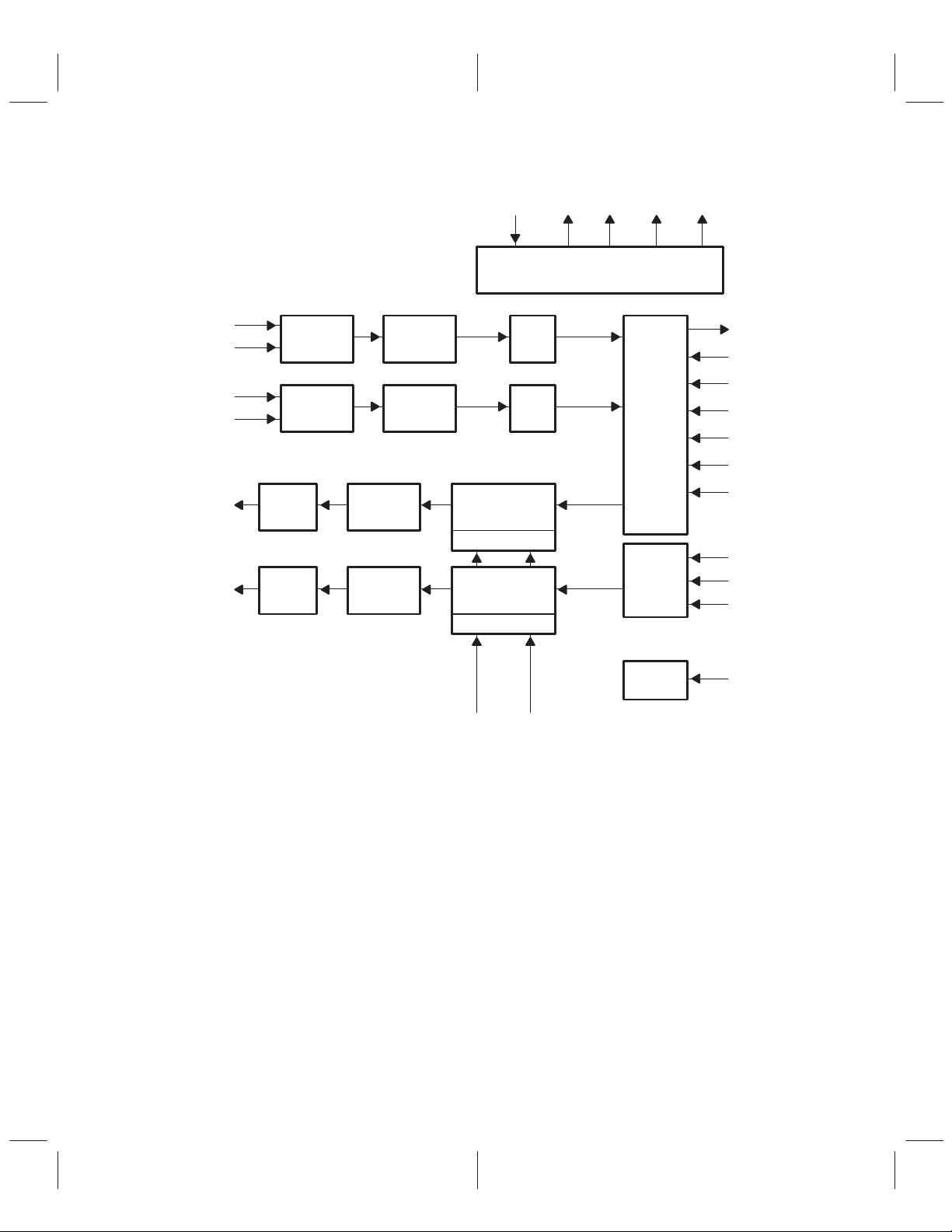
1.2 Functional Block Diagram
AV
SS(REF)
VCOM VREFM VREFP VRFILT
ADC/DAC
Voltage Reference
AINRP
AINRM
AINLP
AINLM
AOUTR
AOUTL
Modulator
Modulator
Analog
LPF
Analog
LPF
ADC
ADC
Decimation
Decimation
Digital
Modulator
Digital
Modulator
ADC
Filter
ADC
Filter
DAC
Interpolation
Filter
De-Emphasis
DAC
Interpolation
Filter
De-Emphasis
DEM0
ADC
HPF
ADC
HPF
DEM1
Serial
Port
I/O
Interface
Control
Clock
Generator
SDOUT
SDIN
SCLK
LRCLK
MOD0
MOD1
MOD2
PDN_RSTB
SPDMODE
TEST
MCLK
1–2
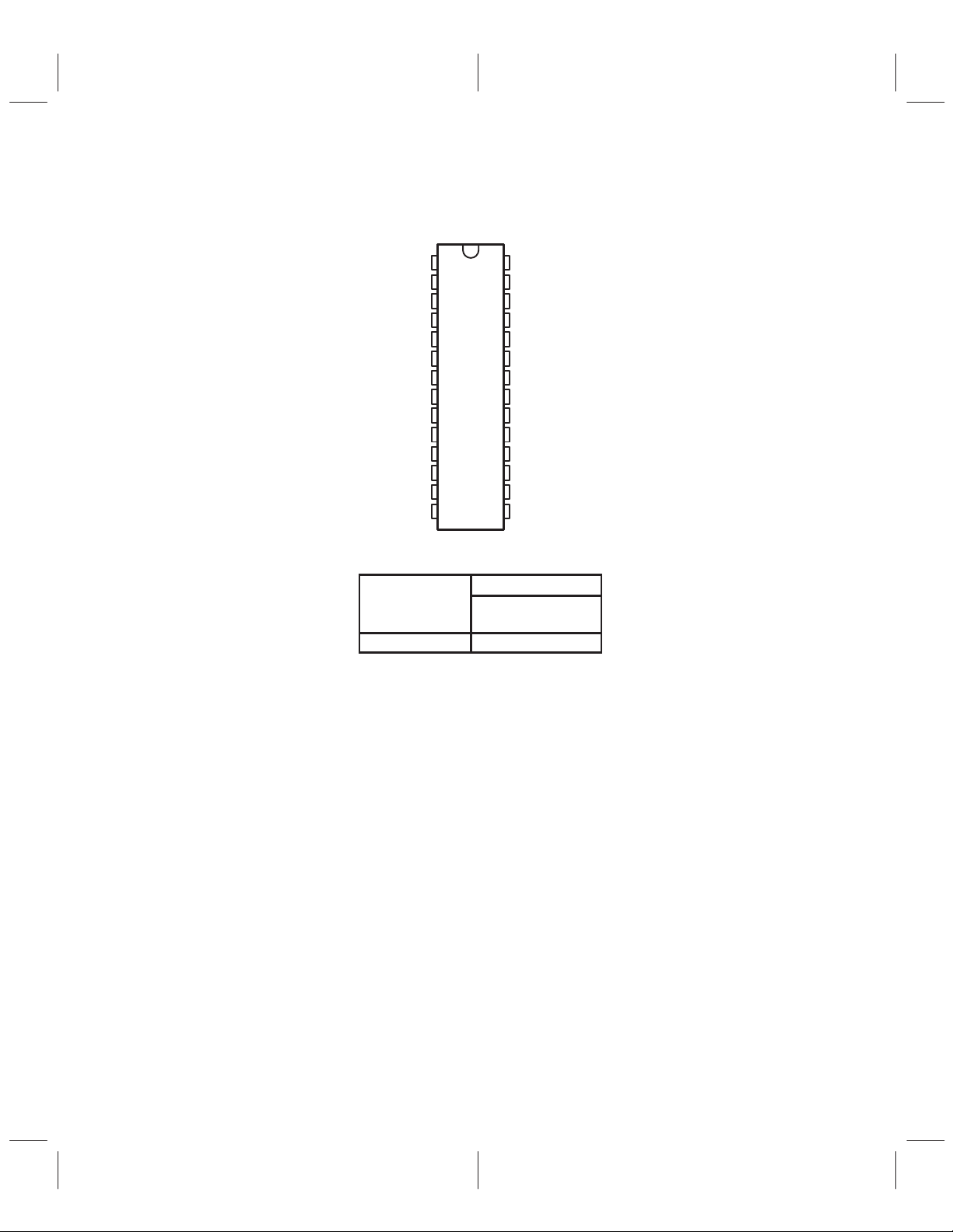
1.3 Terminal Assignments
DB PACKAGE
(TOP VIEW)
1.4 Ordering Information
AINLM
AINLP
VREFP
VREFM
VRFILT
AV
SS(REF)
AV
MOD2
MOD1
MOD0
DV
SDIN
SDOUT
SCLK
0°C to 70°C TLC320AD77C
T
SS
SS
A
1
2
3
4
5
6
7
8
9
10
11
12
13
14
AINRM
28
AINRP
27
AOUTR
26
VCOM
25
AOUTL
24
AV
23
TEST
22
SPDMODE
21
PDN_RSTB
20
DEM1
19
DEM0
18
DV
17
16
LRCLK
15
MCLK
PACKAGE
SMALL OUTLINE
DD
DD
(DB)
1–3
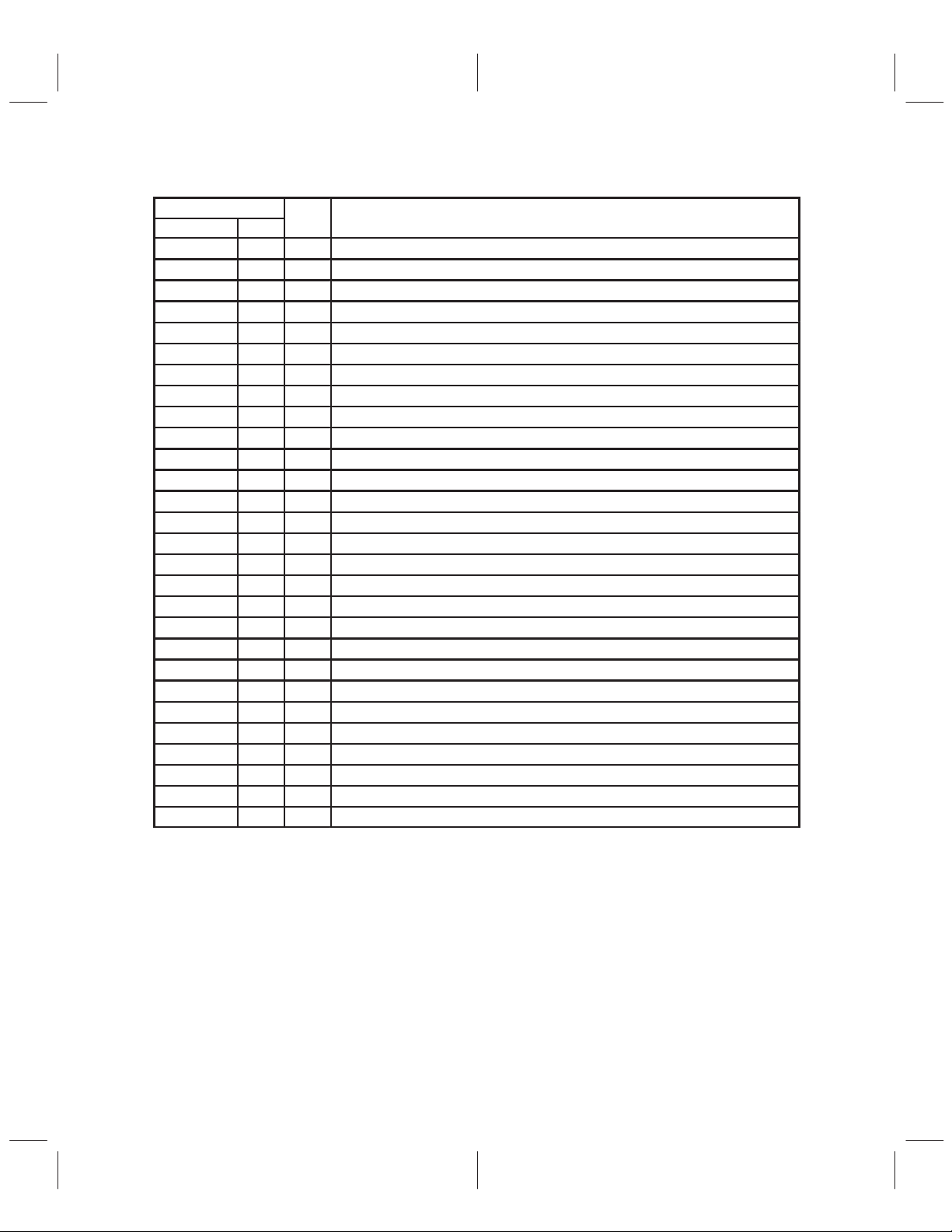
1.5 Terminal Functions
I/O
DESCRIPTION
TERMINAL
NAME NO.
AINLM 1 I ADC analog differential negative input, left channel
AINLP 2 I ADC analog differential positive input, left channel
AINRM 28 I ADC analog differential negative input, right channel
AINRP 27 I ADC analog dif ferential positive input, right channel
AOUTL 24 O DAC analog output, left channel
AOUTR 26 O DAC analog output, right channel
AV
DD
AV
SS
AV
SS(REF)
DEM0 18 I De-emphasis selection
DEM1 19 I De-emphasis selection
DV
DD
DV
SS
LRCLK 16 I Left/right clock
MCLK 15 I Master clock
MOD0 10 I Serial interface selection
MOD1 9 I Serial interface selection
MOD2 8 I Serial interface selection
PDN_RSTB 20 I Power down/reset
SCLK 14 I Shift or bit clock
SDIN 12 I Serial data DAC input
SDOUT 13 O Serial data ADC output
SPDMODE 21 I Sampling frequency selection
TEST 22 Reserved, manufacturing test pin. Test should be connected to DVSS.
VCOM 25 O Common mode reference, provides a 1.5-V reference voltage (DAC only)
VREFM 4 O ADC/DAC negative reference voltage
VREFP 3 O ADC/DAC positive reference voltage
VRFILT 5 O Voltage reference low pass noise filter
23 Analog voltage supply
7 Analog voltage ground
6 I Analog ground voltage reference
17 Digital voltage supply
11 Digital ground
1–4

2 Functional Description
2.1 ADC Channel
To produce excellent common-mode rejection of unwanted signals, the analog signal is processed
differentially until it is converted to digital data. A single-ended input signal must be converted into a
differential input and filtered with a single-pole antialiasing filter before entering the ADC input. (See
Section 2.7,
2s-complement format, corresponding to the analog signal input. There is a high-pass filter to get rid of any
offset that the ADC modulator may have caused. These digital words, representing sampled values of the
analog input signal, are then clocked out the serial port, SDOUT, according to one of the eight allowable
serial port protocols.
ADC Analog Input
2.2 DAC Channel
SDIN receives a serial data word whose length is specified by one of the eight allowable serial port protocols,
selected by the serial mode pins. The serial port latches the data on an edge of SCLK. The data goes through
the sigma-delta DAC comprised of digital interpolation filters and a seventh order, 1-bit digital modulator.
This oversampled signal is then passed through a switched capacitor FIR filter and RC low-pass filter which
smoothes the output waveform, and performs the differential to single-ended conversion. The DAC outputs
a stereo single-ended, inverted signal. This signal should be passed through an inverting,
pseudo-differential, external low-pass filter , where the VCOM reference is subtracted out. (See Section 2.8,
DAC Analog Output
).
2.3 Serial Interface
The digital serial interface consists of a serial port, shift clock (SCLK), left/right frame synchronization clock
(LRCLK), ADC-channel data output (SDOUT), and DAC-channel data input (SDIN). One of 8 different serial
port modes may be selected including IIS, right/left justified, left/left justified, and a DSP mode for word
lengths ranging from 16 to 24 bits. See Section 2.14,
interface formats.
). The ADC converts the signal into discrete output digital words in
Serial Interface Formats
for a description of serial
2.4 Sampling Frequency
The sampling or conversion frequency is designated by the MCLK rate by the following equation.
= MCLK frequency/ (256 or 384).
f
s
See Section 2.14,
of 256 f
or 384 fs.
s
Serial Interface Formats
for more information on the option of selecting an MCLK rate
2.5 Speed Mode Options
In normal-speed mode (SPDMOD = 0), sampling frequencies ranging from 16 kHz up to 48 kHz should be
used to achieve optimum performance.
In high-speed mode (SPDMOD = 1) the sampling frequencies are greater than 48 kHz and up to 96 kHz.
2.6 Voltage Reference
In order to achieve excellent noise rejection, a pseudo-differential reference is used with external capacitors
connected to a differential low-pass filter. The application schematic shows the necessary capacitors
needed to complete the filters found on the device. See Section 5,
schematic for the voltage reference.
Application Information
for the application
2–1

2.7 ADC Analog Input
The ADC accepts a differential input with a maximum value that does not exceed approximately 4 Vpp. See
Section 5.1,
recommended external analog front end.
Single-Ended to Differential External Analog Front-End Circuit
for a description of the
2.8 DAC Analog Output
The DAC outputs a single-ended signal with a max value of 0.7 Vrms. See Section 5.2,
Back-End Circuit
for a description of the recommended back-end circuit.
External Analog
2.9 Sigma-Delta ADC
The sigma-delta ADC is a third order modulator with 128 times oversampling in normal speed operation.
The ADC provides high resolution and low noise performance using over-sampling techniques.
2.10 Decimation Filter
The decimation filter reduces the digital data rate to the sampling rate. This is accomplished by decimating
with a ratio of 1:128. The output of this filter is a 2s complement 16-, 20-, 24-bit word clocking at the sample
rate selected.
2.11 Sigma-Delta DAC
The sigma-delta DAC is a seventh order modulator with 128 times oversampling. The DAC provides
high-resolution, low noise, from a 1-bit converter using over-sampling techniques.
2.12 Interpolation Filter
The interpolation filter resamples the digital data at a rate 128 times the incoming sample rate. The
high-speed data output is then used in the sigma-delta DAC.
2.13 De-emphasis
De-emphasis is supported for three sampling rates: 32 kHz, 44.1 kHz, and 48 kHz and selected with the
DEM0 and DEM1 pins.
2.14 Serial Interface Formats
The TLC320AD77C operates only in slave mode. It requires externally supplied MCLK (master clock), and
LRCLK (left/right clock), and SCLK (shift clock) inputs. There are two options for selecting the clock rates.
If a 384 f
selected, then a LRCLK of 64 SCLKs must be supplied.
The TLC320AD77C is compatible with eight different serial interfaces. Available interface options are IIS,
right justified, left justified, and DSP frame. The following table indicates how the eight options are selected
using the MOD0, MOD1, and MOD2 pins. All serial interface options at either 16-, 20-, or 24-bits can operate
with SCLK at 48*f
MCLK rate is selected, then a LRCLK frame of 48 SCLKs must be supplied. If a 256 fs MCLK is
s
• A detection circuit automatically senses at which rate the MCLK is operating.
• The MCLK and SCLK must be synchronous and their edges must be at least 3 ns apart.
• If the LRCLK phase changes more than 10 MCLKs then the device automatically resets.
or 64*fs except for the 16-bit DSP mode which should use SCLK = 64 fs.
s
2–2

MODE MOD2 PIN MOD1 PIN MOD0 PIN SERIAL INTERFACE SDIN (DAC)/SDOUT (ADC)
0 0 0 0 16-bit, MSB first, right justified/left justified
1 0 0 1 20-bit, MSB first, right justified/left justified
2 0 1 0 24-bit, MSB first, right justified/left justified
3 0 1 1 16-bit IIS
4 1 0 0 20-bit IIS
5 1 0 1 24-bit IIS
6 1 1 0 16-bit MSB first, left justified/left justified
7 1 1 1 16-bit DSP frame (see Note 1)
NOTE 1: For the 16-bit DSP frame use SCLK = 64 fs.
2.14.1 MSB First Right/Left Justified Format
SCLK
LRCLK = f
SDIN
SDOUT
s
LSB
MSB
MSBX LSB MSBX
LSB MSB LSB
Left Channel Right Channel
Figure 2–1. MSB First Right/Left Justified (for 16-, 20-, and 24-bits)
Note the following characteristics of this protocol.
• Left channel data is valid when LRCLK is high.
• The SDIN (recorded data) data is justified to the trailing edge of LRCLK
• The SDOUT MSB (playback data) is transmitted at the same time as the LRCLK edge, and
captured at the very next rising edge of SCLK.
• If LRCLK phase changes by more than 10 MCLKs, then the device is automatically reset.
2–3

2.14.2 IIS-Compatible Serial Format
SCLK
LRCLK = f
SDIN
SDOUT
s
MSBX
MSBX
Left Channel Right Channel
LSB
LSB
MSBX
MSBX
LSB
LSB
Figure 2–2. IIS-Compatible Serial Format (for 16-, 20-, and 24-bits)
Note the following characteristics of this protocol.
• Left channel data is valid when LRCLK is low.
• SDIN is sampled with the rising edge of SCLK.
• SDOUT is transmitted on the falling edge of SCLK.
• If LRCLK phase changes by more than 10 MCLKs, then the device is automatically reset.
2.14.3 MSB Left Justified Serial Interface Format
SCLK
LRCLK = f
SDIN
SDOUT
s
MSB
MSB
LSB
LSB
Left Channel Right Channel
MSB
MSB
LSB
LSB
Figure 2–3. MSB Left Justified Serial Interface Format (for 16-bits)
Note the following characteristics of this protocol.
• Left channel data is valid when LRCLK is high.
• The SDIN data is justified to the leading edge of LRCLK.
• The MSBs are valid at the same time as the LRCLK edge for SDOUT, and captured at the very
next rising edge of SCLK for SDIN.
2–4

2.14.4 DSP Compatible Serial Interface Format
SPDMODE
SCLK
LRCLK = f
SDIN
SDOUT
s
15 14 13 15 14 130 0
15 14 13 15 14 130 0
Left Channel
(MSB = 15)
Right Channel
(MSB = 15)
Figure 2–4. DSP Compatible Serial Interface Format (for 16-bits)
Note the following characteristics of this protocol.
• MCLK = 256 F
only
s
• SCLK = 64 times the sampling frequency.
• Serial data is sampled with the falling edge of SCLK.
• Serial data is transmitted on the rising edge of SCLK.
2.15 Sampling Frequency Ranges
The TLC320AD77C supports two sampling frequency ranges.
• When in the normal option ranging from 16 kHz up to 48 kHz, SPDMOD = low is used.
• When in the fast option ranging from greater than 48 kHz up to 96 kHz, SPDMOD = high is used.
NOTE:
The high speed clocks should never be applied while SPDMOD is low in order to
avoid glitches in the DAC and ADC outputs.
T able 2–1. Example Master Clock Frequency Rates
SAMPLING RATE FREQUENCY
(kHz)
32 8.192 MHz 12.2880 MHz 0
44.1 11.2896 MHz 16.9340 MHz 0
48 12.2880 MHz 18.432 MHz 0
64 16.384 MHz 24.576 MHz 1
88.2 22.579 MHz 33.868 MHz 1
96 24.576 MHz 36.864 MHz 1
MCLK FREQUENCY
256 f
s
384 f
s
2.16 Power Sequences
2.16.1 Initial Power Up
For initial power up, the ADC and DAC outputs are valid after the 150 ms settling time required for the analog
stages. Holding the power down pin low while ramping up the power supplies is recommended to avoid
glitches in the DAC output.
2–5

2.16.2 Power Down/Reset
The TLC320AD77C is capable of entering a stand-by mode at reduced power when no activity is required.
To initiate the reset sequence, PDN_RSTB is held low for a minimum of 10 ns. As long as the pin is held
low, the device is in the power-down state.
In order for the dynamic logic to be properly powered down, the clocks should not be stopped before the
PDN_RSTB pin goes low. Otherwise, the device may drain additional supply current.
2.16.3 Reinitialization Sequence
When PDN_RSTB is returned to high, the device begins a reinitialization sequence after all clocks are
active. The output data becomes valid after a minimum of 128 LRCLK cycles after the pin is pulled high.
During the initialization sequence the outputs of the DAC and ADC are invalid.
Any change in the control lines (MOD0, MOD1, MOD2, DEM0, DEM1, SPDMOD, PDN_RST) or phase shift
in LRCLK triggers the reinitialization sequence.
In order for the dynamic logic to be properly powered down, the clocks should not be stopped before the
PDN_RSTB pin goes low. Otherwise, the device may drain additional supply current.
2.17 DAC De-Emphasis Filter
De-emphasis is only supported for three sampling rates (fs): 32 kHz, 44.1 kHz, and 48 kHz in normal speed
operation. The DEM0 and DEM1 pins select the filter coefficients and enable or disable the filter . Figure 2–5
illustrates the de-emphasis filtering characteristics.
0
–10
Response – dB
3.18
(50 µs)
f – Frequency – kHz
De-emphasis
10.6
(15 µs)
Figure 2–5. De-Emphasis Characteristics
2.17.1 De-Emphasis Selection
De-emphasis control is achieved using the DEM1 and DEM0 pins. The pin control is defined in the following
table.
DEM 1 DEM 0 DE-EMPHASIS
0 0 32 kHz
0 1 44.1 kHz
1 0 48 kHz
1 1 Off
2–6

3 Specifications
3.1 Absolute Maximum Ratings Over Operating Free-Air Temperature Range
(Unless Otherwise Noted)
Analog supply voltage range, AVDD –0.3 V to 4.2 V. . . . . . . . . . . . . . . . . . . . . . . . . . . . . . .
Digital supply voltage range, DVDD –0.3 V to 4.2 V. . . . . . . . . . . . . . . . . . . . . . . . . . . . . . . .
Analog input voltage range –0.3 V to AVDD + 0.3 V. . . . . . . . . . . . . . . . . . . . . . . . . . . . . . .
Digital input voltage range –0.3 V to DV
Operating free-air temperature range, TA 0°C to 70°C. . . . . . . . . . . . . . . . . . . . . . . . . . . .
Storage temperature range, T
†
Stresses beyond those listed under “absolute maximum ratings” may cause permanent damage to the device. These
are stress ratings only and functional operation of the device at these or any other conditions beyond those indicated
under “recommended operating conditions” is not implied. Exposure to absolute-maximum-rated conditions for
extended periods may affect device reliability.
3.2 Recommended Operating Conditions, TA = 25°C,
= DVDD = 3.3 V ± 10%, fs = 44.1 kHz
AV
DD
Analog supply voltage, A VDD (see Note 1) 3 3.3 3.6 V
Digital supply voltage, DVDD (see Note 1) 3 3.3 3.6 V
Operating free-air temperature range, T
NOTE 1: Voltages at analog inputs and outputs and AVDD are with respect to ground.
3.3 Electrical Characteristics, TA = 25°C, AVDD = DVDD = 3.3 V ± 10%,
f
= 44.1 kHz
s
PARAMETER MIN TYP MAX UNIT
Analog supply current
Digital supply current
Power dissipation
NOTE 2: If clocks are turned off.
†
–65°C to 150°C. . . . . . . . . . . . . . . . . . . . . . . . . . . . . . . . .
stg
A
Operating 30 mA
Power down (see Note 2) 150 µA
Operating 20 mA
Power down (see Note 2) 1 µA
Operating 160 mW
Power down 360 µW
+ 0.3 V. . . . . . . . . . . . . . . . . . . . . . . . . . . . . . .
DD
MIN NOM MAX UNIT
0 70 °C
3.3.1 Static Digital Specifications, TA = 25°C, AVDD = DVDD = 3.3 V ± 10%
PARAMETER MIN MAX UNIT
V
High-level input voltage 2 3.6 V
IH
V
Low-level input voltage –0.3 0.8 V
IL
V
High-level output voltage (IO = –1 mA) 2.4 V
OH
V
Low-level output voltage (IO = 4 mA) 0.4 V
OL
I
Input leakage current –10 10 µA
lkg
C
Load capacitance, SDOUT 50 pF
L
3–1

3.3.2 ADC Digital Filter, TA = 25°C, AVDD = DVDD = 3.3 V ± 10%, fs = 44.1 kHz
(see Notes 3 and 4)
PARAMETER TEST CONDITIONS MIN TYP MAX UNIT
ADC Decimation Filter (LPF)
Pass band 20 kHz
Pass band ripple ±0.01 dB
Stop band 24.1 kHz
Stop band attenuation 80 dB
Group delay 720 µs
ADC High-Pass Filter (HPF)
Pass band (–3 dB) 0.87 Hz
Deviation from linear phase 20 Hz to 20 kHz 1.23 degree
NOTES: 3. All the terms characterized by frequency, scale with the chosen sampling frequency, fs.
4. See Figure 4–6 through Figure 4–9 for performance curves on the ADC digital filter.
3.3.3 Analog-to-Digital Converter, TA = 25°C, AVDD = DVDD = 3.3 V, fs = 44.1 kHz
(see Note 3)
PARAMETER TEST CONDITIONS MIN TYP MAX UNIT
SNR Signal-to-noise ratio (EIAJ) A-weighted 100 dB
Dynamic range A-weighted, –60 dB, 1 kHz 100 dB
Signal-to-noise + distortion ratio 20 Hz to 20 kHz 86 dB
Power supply rejection ratio 1 kHz, See Note 5 50 dB
Idle channel tone rejection 120 dB
Intermodulation distortion –80 dB
ADC crosstalk 100 dB
Overall ADC frequency response 20 Hz to 20 kHz –0.1 0.1 dB
Gain error 5%
Gain matching ±0.02 dB
Full-scale differential input voltage 3.6 V
CMRR Common mode rejection ratio 100 dB
pp
NOTES: 3. All the terms characterized by frequency, scale with the chosen sampling frequency, fs.
5. Measured with a 50 mV peak sine wave.
3.3.4 DAC Interpolation Filter, TA = 25°C, AVDD = DVDD = 3.3 V + 10%, fs = 44.1 kHz
(see Notes 3 and 6)
PARAMETER TEST CONDITIONS MIN TYP MAX UNIT
Pass band 0 20 kHz
Pass band ripple ±0.005 dB
Stop band 24.1 kHz
Stop band attenuation 28.8 kHz to 3 MHz 75 dB
Group delay 700 µs
NOTES: 3. All the terms characterized by frequency, scale with the chosen sampling frequency, fs.
3–2
6. See Figure 4–4 and Figure 4–5 for performance curves of the DAC digital filter.

3.3.5 Digital-to-Analog Converter, TA = 25°C, AVDD = 3.3 V, fs = 44.1 kHz,
Input = 1 V
SNR Signal-to-noise ratio (EIAJ) A-weighted 100 dB
Dynamic range
Signal-to-noise + distortion ratio 0 dB, 1 kHz 80 dB
Power supply rejection ratio 1 kHz 50 dB
Idle tone rejection 120 dB
Intermodulation distortion –75 dB
Frequency response –0.5 0.5 dB
Deviation from linear phase ±1.4 degree
DAC crosstalk 100 dB
Full-scale single-ended output voltage AVDD = 3.3 V 1.75 V
NOTE 3: All the terms characterized by frequency, scale with the chosen sampling frequency, fs.
Sine Wave at 1 kHz (see Note 3)
rms
PARAMETER TEST CONDITIONS MIN TYP MAX UNIT
A-weighted, –60 dB,
f = 1 kHz
100 dB
3.3.6 Output Performance Data, TA = 25°C, AVDD = DVDD = 3.3 V ± 10%
PARAMETER TEST CONDITIONS MIN TYP MAX UNIT
Output Driver Loading
R
L
C
L
R
L(COM)
C
L(COM)
NOTES: 7. The output load resistance is coupled through an ac coupled capacitor.
Output load resistance, (see Note 7) 10 kΩ
Output load capacitance 25 pF
Output load resistance, COM (see Note 8) 1 kΩ
Output load capacitance, COM
(see Note 8)
RFILT internal resistance, RFILT
(see Note 9)
8. COM may vary during power down.
9. RFILT should never be used as a voltage reference.
50 pF
1 kΩ
PP
3–3

3.4 Serial Interface Switching Characteristics, T
AVDD = DVDD = 3.3 V ± 10%
PARAMETER MIN TYP MAX UNIT
f
(SCLK)
t
d(LRCLK)
t
d(SDOUT)
t
su(SDIN)
t
h(SDIN)
f
(LRCLK)
NOTE 10: Maximum of 50-pF external load on SDOUT
SCLK frequency 6.144 MHz
Delay time, LRCLK edge to SCLK rising 20 1/(128×fs) ns
Delay time, SDOUT valid from SCLK falling
(see Note 10)
SDIN setup time before SCLK rising edge 20 ns
SDIN hold time from SCLK rising edge 10 ns
LRCLK frequency 16 44.1 96 kHz
MCLK duty cycle 50%
SCLK duty cycle 50%
LRCLK duty cycle 50%
= 25°C,
A
(1/(256×fs))+10 ns
3.5 DSP Serial Interface Switching Characteristics, T
AVDD = DVDD = 3.3 V ± 10% (see Note 11)
PARAMETER MIN TYP MAX UNIT
f
(SCLK)
t
d(FS)
t
w(FSHIGH)
t
d(SDOUT)
t
su(SDIN)
t
h(SDIN)
NOTES: 11. Burst mode is not supported.
SCLK frequency 6.144 MHz
Delay time, SCLK rising to Fs 25 ns
Pulse duration, sync 1/(64×fs) ns
Delay time, SDOUT valid from SCLK rising
(see Note 12)
SDIN and LRCLK setup time before SCLK falling
edge
SDIN and LRCLK hold time from SCLK falling edge 10 ns
SCLK duty cycle 50%
12. Timing parameters for DSP format which samples on the falling edge
20 ns
= 25°C,
A
(1/(256×fs))+10 ns
3–4

4 Parameter Measurement Information
MCLK
t
wH(MCLK)
t
wL(MCLK)
Figure 4–1. Master Clock Timing
SCLK
t
d(LRCLK)
LRCK
t
d(SDOUT)
SDOUT
SDIN
t
su(SDIN)
t
h(SDIN)
Figure 4–2. Right/Left Justified, IIS, Left/Left Justified Serial Protocol Timing
SCLK
LRCLK
SDOUT
SDIN
t
d(FS)
t
w(FSHIGH)
t
d(SDOUT)
t
su(SDIN)
Figure 4–3. DSP Serial Port Timing
t
h(SDIN)
4–1

0
R
–20
–40
–60
Amplitude – dB
–80
–100
0f
0.1
0.05
0
Amplitude – dB
–0.05
s/2
1 f
s
2 f
s
f – Frequency – Hz
3 f
s
4 f
s
Figure 4–4. DAC Filter Overall Frequency Characteristics
5 f
s
–0.1
0
Figure 4–5. DAC Digital Filter Passband Ripple Characteristics
50
0
–50
–100
Amplitude – dB
–150
–200
02 fs4 f
0.1 f
s
0.2 f
s
f – Frequency – Hz
s
f – Frequency – Hz
6 f
0.3 f
s
s
8 f
s
Figure 4–6. ADC Digital Filter Characteristics
0.4 f
10 f
s
s
0.5 f
12 f
s
s
4–2

0
–20
–40
–60
Amplitude – dB
–80
–100
0
0.008
0.006
0.004
0.002
Amplitude – dB
0
0.2 f
s
0.4 f
s
f – Frequency – Hz
0.6 f
s
0.8 f
Figure 4–7. ADC Digital Filter Stopband Characteristics
s
1 f
s
–0.002
0
0.2
0
–0.2
–0.4
–0.6
Amplitude – dB
–0.8
–1
0
0.1 f
s
0.2 f
s
f – Frequency – Hz
0.3 f
s
0.4 f
s
Figure 4–8. ADC Digital Filter Passband Characteristics
1 f
s
2 f
f – Frequency – Hz
s
3 f
s
Figure 4–9. ADC High Pass Filter Characteristics
0.5 f
4 f
s
s
4–3

4–4

5 Application Information
5.1 Single-Ended to Differential External Analog Front-End Circuit
(f
= 44.1 kHz)
s
A single-ended to differential external analog front-end example circuit is shown in Figure 5–1. It biases the
input signal around A VDD/2 and applies the maximum input signal of 0.7 Vrms. The device sees a full-scale
differential input voltage of approximately 4 V
be scaled accordingly to ensure a max ADC input of approximately 4 V
and R6 provide a single-pole low-pass antialiasing filter to attenuate unwanted frequencies. If the user
chooses to supply a single-ended input directly to the device (2 V
degraded.
. For other maximum input signals, the ratio of R2/R1 can
pp
. As required by the ADC, R5, C4,
pp
max), performance will be significantly
pp
Right Channel
Analog Input
0.7 V
rms
C1
211
47 µF
AVDD/2
R1
10 kΩ
C2
2
1
10 pF
R2
2
1
10 kΩ
5 V
2
U3:A
8
2
_
3
+
4
GND
R3
1
1
10 kΩ
C3
2
1
10 pF
R4
2
1
10 kΩ
U3:B
6
2
_
7
5
+
R5
1
499 Ω
Antialiasing
Filter
R6
2
1
499 Ω
2
1
2
C4
1000 pF
Figure 5–1. Analog Front End (right channel) for 0.7 Vrms Input
AINRM
4 V
AINRP
PP
5–1

5.2 External Analog Back-End Circuit (fs = 44.1 kHz)
For specified performance, the output should be taken between VCOM and AOUTR (or AOUTL). At pins
AOUTR and AOUTL the output is an inverted analog representation of the digital input signal. It is advisable
to add a low-pass filter to the output of the TLC320AD77C to eliminate high frequency noise >80 kHz. See
Figure 5–2 for the recommended analog back-end circuit. The output of this circuit provides the user with
a noninverted signal.
R10
21
0.7 V
rms
AOUTR
VCOM
10 kΩ
R9
21
R7
10 kΩ
C5
33 pF
3.3 VA_Ground
(AD77 AVSS @ U2–7)
10 kΩ
21
2
1
2
R8
10 kΩ
1
Figure 5–2. Analog Back End (right channel) for 0.7 Vrms Output
2
3
33 pF
5 V
_
+
GND
C6
8
4
21
C20
21
1
47 µF
3.3 VA_Ground
R11
100 kΩ
2
R12
221 Ω
21
Right Channel DAC
Output 0.7 V
rms
5–2

FB1
V
Filter
ref
VREFM
C9
0.1 µF
1
C8
0.1 µF
2
1
C7
1 µF
VREFP
AV
21
SS(REF)
2
1
2
7
23
11
17
14
15
16
18
19
8
9
10
21
20
22
28
27
1
2
12
AV
SS
AV
DD
DV
SS
DV
DD
SCLK
MCLK
LRCLK
DEM0
DEM1
MOD2
MOD1
MOD0
SPDMODE
PDN_RSTB
TEST
AINRM
AINRP
AINLM
AINLP
SDIN
TLC320AD77
U2
AV
VREFM
VREFP
SS(REF)
VRFILT
SDOUT
AOUTR
VCOM
AOUTL
4
3
6
5
13
26
25
24
VRFILT
2
1
C10
15 µF
1
C11
0.1 µF
2
Figure 5–3. Voltage Reference Connections
5–3

5–4

Appendix A
Mechanical Data
DB (R-PDSO-G**) PLASTIC SMALL-OUTLINE PACKAGE
28 PINS SHOWN
0,65
28
0,38
0,22
15
0,15
M
1
2,00 MAX
DIM
A
PINS **
A MAX
A MIN
8
3,30
2,70
14
0,05 MIN
14
6,50
5,60
5,00
Seating Plane
6,50
7,50
5,905,90
6,90
8,20
7,40
2016
0,10
8,50
24
28
10,50
9,907,90
0,15 NOM
Gage Plane
0°–8°
30
10,50
9,90
0,25
1,03
0,63
38
12,90
12,30
4040065 /C 10/95
NOTES: A. All linear dimensions are in millimeters.
B. This drawing is subject to change without notice.
C. Body dimensions do not include mold flash or protrusion not to exceed 0,15.
D. Falls within JEDEC MO-150
A–1

A–2

IMPORTANT NOTICE
T exas Instruments and its subsidiaries (TI) reserve the right to make changes to their products or to discontinue
any product or service without notice, and advise customers to obtain the latest version of relevant information
to verify, before placing orders, that information being relied on is current and complete. All products are sold
subject to the terms and conditions of sale supplied at the time of order acknowledgement, including those
pertaining to warranty, patent infringement, and limitation of liability.
TI warrants performance of its semiconductor products to the specifications applicable at the time of sale in
accordance with TI’s standard warranty. Testing and other quality control techniques are utilized to the extent
TI deems necessary to support this warranty . Specific testing of all parameters of each device is not necessarily
performed, except those mandated by government requirements.
CERTAIN APPLICATIONS USING SEMICONDUCTOR PRODUCTS MAY INVOLVE POTENTIAL RISKS OF
DEATH, PERSONAL INJURY, OR SEVERE PROPERTY OR ENVIRONMENTAL DAMAGE (“CRITICAL
APPLICATIONS”). TI SEMICONDUCTOR PRODUCTS ARE NOT DESIGNED, AUTHORIZED, OR
WARRANTED TO BE SUITABLE FOR USE IN LIFE-SUPPORT DEVICES OR SYSTEMS OR OTHER
CRITICAL APPLICA TIONS. INCLUSION OF TI PRODUCTS IN SUCH APPLICATIONS IS UNDERST OOD TO
BE FULLY AT THE CUSTOMER’S RISK.
In order to minimize risks associated with the customer’s applications, adequate design and operating
safeguards must be provided by the customer to minimize inherent or procedural hazards.
TI assumes no liability for applications assistance or customer product design. TI does not warrant or represent
that any license, either express or implied, is granted under any patent right, copyright, mask work right, or other
intellectual property right of TI covering or relating to any combination, machine, or process in which such
semiconductor products or services might be or are used. TI’s publication of information regarding any third
party’s products or services does not constitute TI’s approval, warranty or endorsement thereof.
Copyright 1999, Texas Instruments Incorporated
 Loading...