Texas Instruments TLC320AD535PM, TLC320AD535IPM Datasheet
TLC320AD535C/I
Dual Channel V oice/Data Codec
2000 Mixed Signal Products
Data Manual
SLAS202B

IMPORTANT NOTICE
T exas Instruments and its subsidiaries (TI) reserve the right to make changes to their products or to discontinue
any product or service without notice, and advise customers to obtain the latest version of relevant information
to verify, before placing orders, that information being relied on is current and complete. All products are sold
subject to the terms and conditions of sale supplied at the time of order acknowledgement, including those
pertaining to warranty, patent infringement, and limitation of liability.
TI warrants performance of its semiconductor products to the specifications applicable at the time of sale in
accordance with TI’s standard warranty. Testing and other quality control techniques are utilized to the extent
TI deems necessary to support this warranty. Specific testing of all parameters of each device is not necessarily
performed, except those mandated by government requirements.
CERT AIN APPLICATIONS USING SEMICONDUCTOR PRODUCTS MAY INVOLVE POTENTIAL RISKS OF
DEATH, PERSONAL INJURY, OR SEVERE PROPERTY OR ENVIRONMENTAL DAMAGE (“CRITICAL
APPLICATIONS”). TI SEMICONDUCTOR PRODUCTS ARE NOT DESIGNED, AUTHORIZED, OR
WARRANTED TO BE SUITABLE FOR USE IN LIFE-SUPPORT DEVICES OR SYSTEMS OR OTHER
CRITICAL APPLICATIONS. INCLUSION OF TI PRODUCTS IN SUCH APPLICA TIONS IS UNDERSTOOD T O
BE FULLY AT THE CUSTOMER’S RISK.
In order to minimize risks associated with the customer’s applications, adequate design and operating
safeguards must be provided by the customer to minimize inherent or procedural hazards.
TI assumes no liability for applications assistance or customer product design. TI does not warrant or represent
that any license, either express or implied, is granted under any patent right, copyright, mask work right, or other
intellectual property right of TI covering or relating to any combination, machine, or process in which such
semiconductor products or services might be or are used. TI’s publication of information regarding any third
party’s products or services does not constitute TI’s approval, warranty or endorsement thereof.
Copyright 2000, Texas Instruments Incorporated

iii
Contents
Section Title Page
1 Introduction 1–1. . . . . . . . . . . . . . . . . . . . . . . . . . . . . . . . . . . . . . . . . . . . . . . . . . . . . .
1.1 Features 1–1. . . . . . . . . . . . . . . . . . . . . . . . . . . . . . . . . . . . . . . . . . . . . . . . . . .
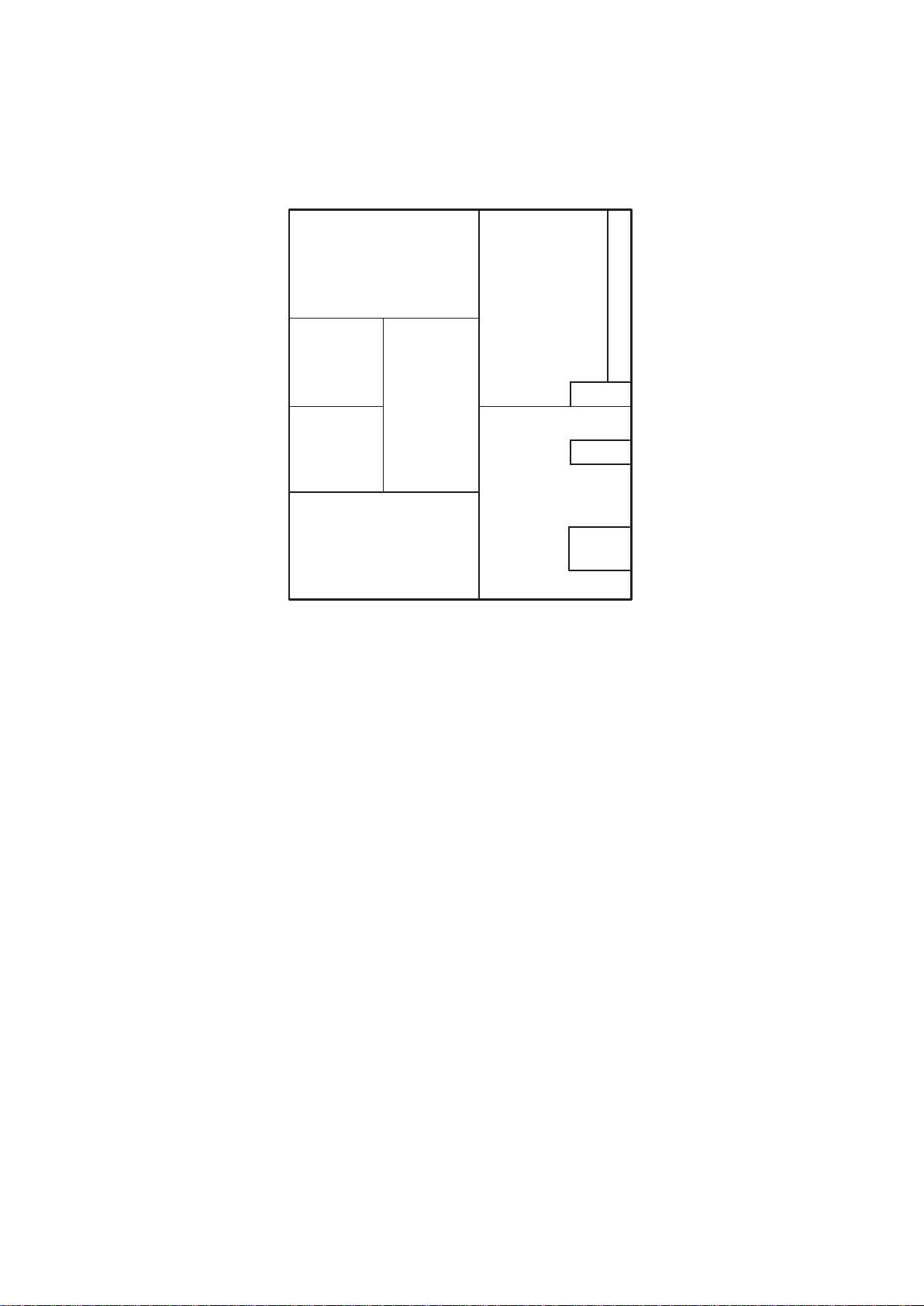
1.2 Functional Block Diagram 1–2. . . . . . . . . . . . . . . . . . . . . . . . . . . . . . . . . . . .
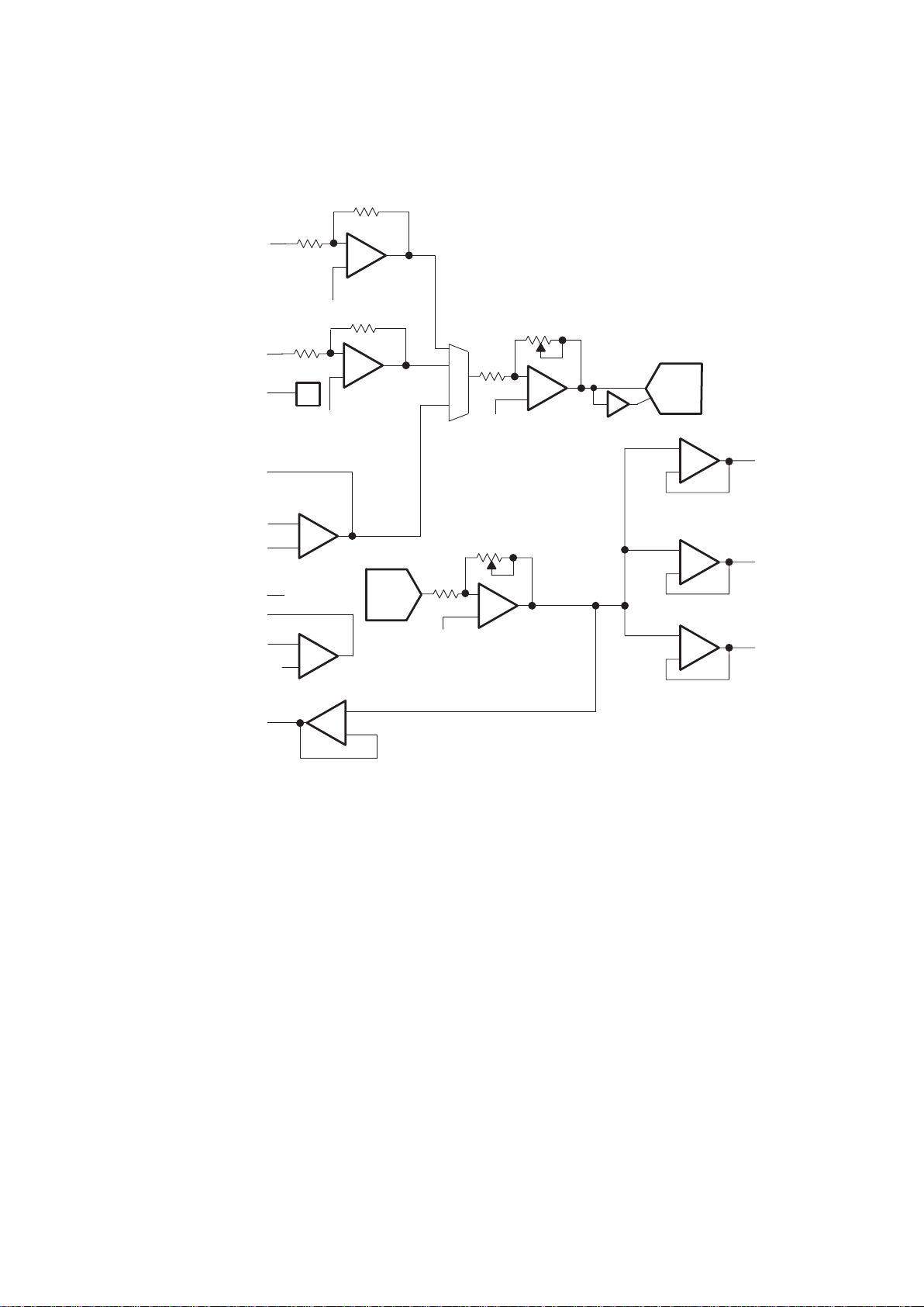
1.3 Voice Channel Codec Logic Diagram 1–3. . . . . . . . . . . . . . . . . . . . . . . . . .
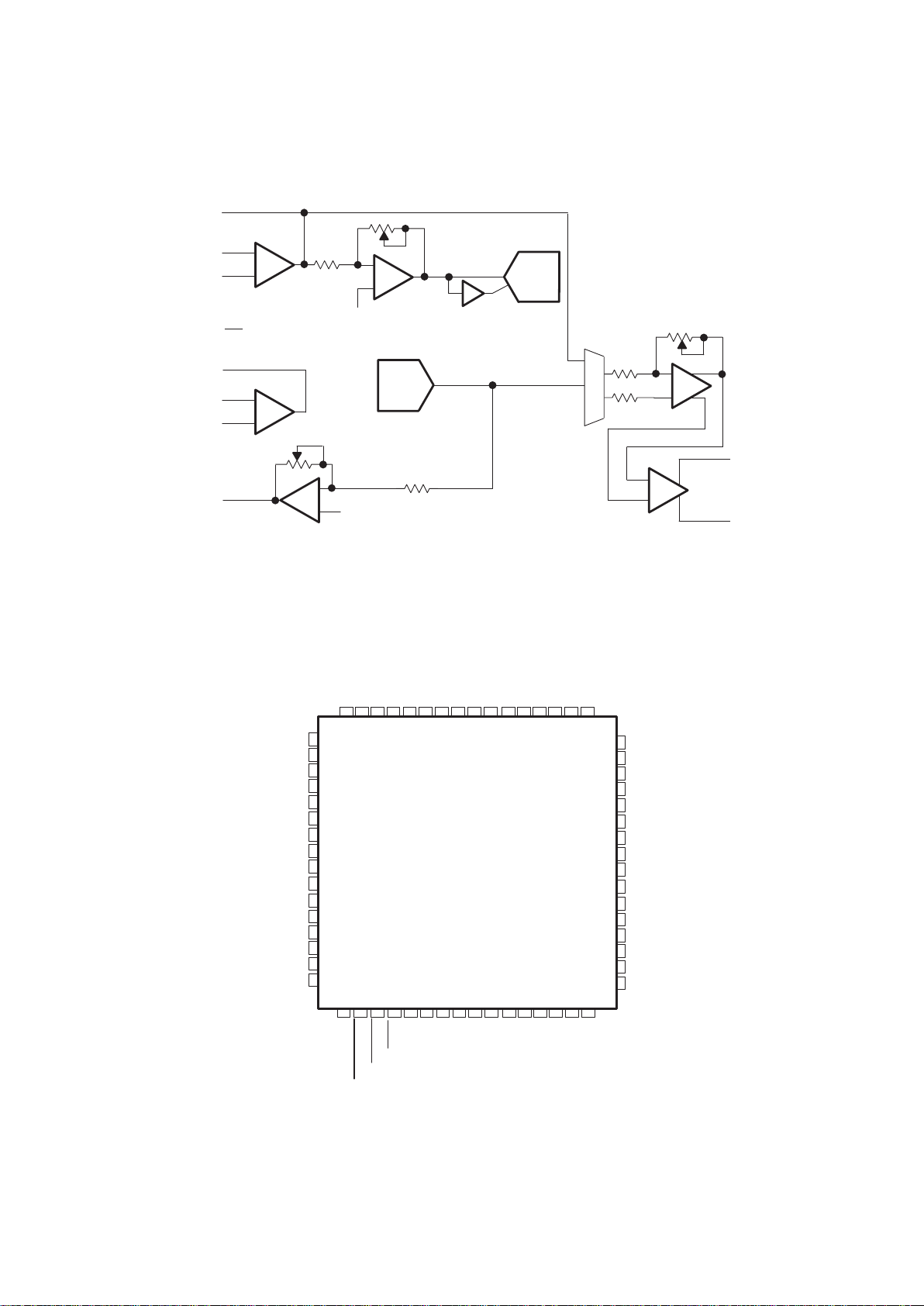
1.4 Data Channel Codec Logic Diagram 1–4. . . . . . . . . . . . . . . . . . . . . . . . . . .
1.5 Terminal Assignments 1–4. . . . . . . . . . . . . . . . . . . . . . . . . . . . . . . . . . . . . . . .
1.6 Ordering Information 1–5. . . . . . . . . . . . . . . . . . . . . . . . . . . . . . . . . . . . . . . . .
1.7 Terminal Functions 1–5. . . . . . . . . . . . . . . . . . . . . . . . . . . . . . . . . . . . . . . . . .
2 Functional Description 2–1. . . . . . . . . . . . . . . . . . . . . . . . . . . . . . . . . . . . . . . . . . . .
2.1 Device Requirements and System Overview 2–1. . . . . . . . . . . . . . . . . . . .
2.2 Codec Functions 2–1. . . . . . . . . . . . . . . . . . . . . . . . . . . . . . . . . . . . . . . . . . . .
2.3 Hybrid Functions 2–1. . . . . . . . . . . . . . . . . . . . . . . . . . . . . . . . . . . . . . . . . . . .
2.4 Voice Channel Analog 2–1. . . . . . . . . . . . . . . . . . . . . . . . . . . . . . . . . . . . . . . .
2.5 Miscellaneous Logic and Other Circuitry 2–1. . . . . . . . . . . . . . . . . . . . . . . .
3 Codec Functional Description 3–1. . . . . . . . . . . . . . . . . . . . . . . . . . . . . . . . . . . . .
3.1 Operating Frequencies 3–1. . . . . . . . . . . . . . . . . . . . . . . . . . . . . . . . . . . . . . .
3.2 ADC Signal Channel 3–1. . . . . . . . . . . . . . . . . . . . . . . . . . . . . . . . . . . . . . . . .
3.3 DAC Signal Channel 3–1. . . . . . . . . . . . . . . . . . . . . . . . . . . . . . . . . . . . . . . . .
3.4 Sigma-Delta ADC 3–1. . . . . . . . . . . . . . . . . . . . . . . . . . . . . . . . . . . . . . . . . . .
3.5 Decimation Filter 3–1. . . . . . . . . . . . . . . . . . . . . . . . . . . . . . . . . . . . . . . . . . . .
3.6 Sigma-Delta DAC 3–2. . . . . . . . . . . . . . . . . . . . . . . . . . . . . . . . . . . . . . . . . . .
3.7 Interpolation Filter 3–2. . . . . . . . . . . . . . . . . . . . . . . . . . . . . . . . . . . . . . . . . . .
3.8 Analog and Digital Loopbacks 3–2. . . . . . . . . . . . . . . . . . . . . . . . . . . . . . . . .
3.9 Software Power Down 3–2. . . . . . . . . . . . . . . . . . . . . . . . . . . . . . . . . . . . . . .
3.10 Reset Circuit 3–2. . . . . . . . . . . . . . . . . . . . . . . . . . . . . . . . . . . . . . . . . . . . . . . .
3.11 Test Module 3–3. . . . . . . . . . . . . . . . . . . . . . . . . . . . . . . . . . . . . . . . . . . . . . . .
4 Serial Communications 4–1. . . . . . . . . . . . . . . . . . . . . . . . . . . . . . . . . . . . . . . . . . .
4.1 Primary Serial Communication 4–1. . . . . . . . . . . . . . . . . . . . . . . . . . . . . . . .
4.1.1 FS High Mode Primary Communication Timing 4–2. . . . . . . . .
4.1.2 FS Low Mode Primary Communication Timing 4–2. . . . . . . . . .
4.2 Secondary Serial Communication 4–3. . . . . . . . . . . . . . . . . . . . . . . . . . . . .
4.2.1 FS High Mode Secondary Communication Timing 4–4. . . . . . .
4.2.2 FS Low Mode Secondary Communication Timing 4–4. . . . . . .
5 Specifications 5–1. . . . . . . . . . . . . . . . . . . . . . . . . . . . . . . . . . . . . . . . . . . . . . . . . . . .
5.1 Absolute Maximum Ratings Over Operating Free-Air
Temperature Range 5–1. . . . . . . . . . . . . . . . . . . . . . . . . . . . . . . . . . . . . . . . . .
5.2 Recommended Operating Conditions 5–1. . . . . . . . . . . . . . . . . . . . . . . . . .

iv
5.3 Electrical Characteristics Over Operating Free-Air Temperature
Range, DV
DD
= 5 V/3.3 V, xAVDD = 5 V/3.3 V,
MV
DD
= 5 V/3.3 V 5–1. . . . . . . . . . . . . . . . . . . . . . . . . . . . . . . . . . . . . . . . . . .
5.3.1 Digital Inputs and Outputs, f
s
= 8 kHz,
Outputs Not Loaded 5–1. . . . . . . . . . . . . . . . . . . . . . . . . . . . . . . . .
5.3.2 ADC Channel, f
s
= 8 kHz 5–2. . . . . . . . . . . . . . . . . . . . . . . . . . . .
5.3.3 ADC Dynamic Performance, f
s
= 8 kHz 5–2. . . . . . . . . . . . . . . .
5.3.3.1 ADC Signal-to-Noise 5–2. . . . . . . . . . . . . . . . . . . . .
5.3.3.2 ADC Signal-to-Distortion 5–2. . . . . . . . . . . . . . . . . .
5.3.3.3 ADC Signal-to-Distortion + Noise 5–2. . . . . . . . . .
5.3.4 ADC Characteristics 5–3. . . . . . . . . . . . . . . . . . . . . . . . . . . . . . . .
5.3.5 DAC Channel, f
s
= 8 kHz 5–3. . . . . . . . . . . . . . . . . . . . . . . . . . . .
5.3.6 DAC Dynamic Performance 5–3. . . . . . . . . . . . . . . . . . . . . . . . . .
5.3.6.1 DAC Signal-to-Noise 5–3. . . . . . . . . . . . . . . . . . . . .
5.3.6.2 DAC Signal-to-Distortion 5–3. . . . . . . . . . . . . . . . . .
5.3.6.3 DAC Signal-to-Distortion + Noise 5–3. . . . . . . . . .
5.3.7 DAC Characteristics 5–4. . . . . . . . . . . . . . . . . . . . . . . . . . . . . . . .
5.3.8 Logic DC Electrical Characteristics 5–4. . . . . . . . . . . . . . . . . . . .
5.3.9 Power Supply Rejection 5–4. . . . . . . . . . . . . . . . . . . . . . . . . . . . .
5.3.10 Power Supply 5–4. . . . . . . . . . . . . . . . . . . . . . . . . . . . . . . . . . . . . .
5.3.11 Reset Circuit 5–5. . . . . . . . . . . . . . . . . . . . . . . . . . . . . . . . . . . . . . .
5.3.12 Flash Write Enable Circuit 5–5. . . . . . . . . . . . . . . . . . . . . . . . . . .
5.3.13 8-Ω Drive 5–5. . . . . . . . . . . . . . . . . . . . . . . . . . . . . . . . . . . . . . . . . .
5.4 Timing Characteristics 5–5. . . . . . . . . . . . . . . . . . . . . . . . . . . . . . . . . . . . . . .
5.4.1 Timing Requirements 5–5. . . . . . . . . . . . . . . . . . . . . . . . . . . . . . . .
5.4.2 Switching Characteristics 5–5. . . . . . . . . . . . . . . . . . . . . . . . . . . .
5.5 Parameter Measurement Information 5–6. . . . . . . . . . . . . . . . . . . . . . . . . .
6 Application Information 6–1. . . . . . . . . . . . . . . . . . . . . . . . . . . . . . . . . . . . . . . . . . .
A Programmable Register Set A–1. . . . . . . . . . . . . . . . . . . . . . . . . . . . . . . . . . . . . . .
B Mechanical Data B–1. . . . . . . . . . . . . . . . . . . . . . . . . . . . . . . . . . . . . . . . . . . . . . . . . .

v
List of Illustrations
Figure Title Page
4–1 Primary Communication DIN and DOUT Data Format 4–1. . . . . . . . . . . . . . . . .
4–2 FS High Mode Primary Serial Communication Timing 4–2. . . . . . . . . . . . . . . . . .
4–3 FS Low Mode Primary Serial Communication Timing 4–2. . . . . . . . . . . . . . . . . .
4–4 Secondary Communication DIN and DOUT Data Format 4–3. . . . . . . . . . . . . . .
4–5 FS Output During Software Secondary Serial Communication Request
(FS High Mode) 4–4. . . . . . . . . . . . . . . . . . . . . . . . . . . . . . . . . . . . . . . . . . . . . . . .
4–6 FS Output During Software Secondary Serial Communication Request
(FS Low Mode) 4–4. . . . . . . . . . . . . . . . . . . . . . . . . . . . . . . . . . . . . . . . . . . . . . . . .
5–1 Serial Communication Timing for FS High Mode 5–6. . . . . . . . . . . . . . . . . . . . . .
5–2 ADC Decimation Filter Response 5–6. . . . . . . . . . . . . . . . . . . . . . . . . . . . . . . . . . .
5–3 ADC Decimation Filter Passband Ripple 5–7. . . . . . . . . . . . . . . . . . . . . . . . . . . . .
5–4 DAC Interpolation Filter Response 5–7. . . . . . . . . . . . . . . . . . . . . . . . . . . . . . . . . .
5–5 DAC Interpolation Filter Passband Ripple 5–8. . . . . . . . . . . . . . . . . . . . . . . . . . . .
6–1 Functional Block of a Typical Application 6–1. . . . . . . . . . . . . . . . . . . . . . . . . . . . .
6–2 Voice Channel Codec Typical Application 6–2. . . . . . . . . . . . . . . . . . . . . . . . . . . .
6–3 Data Channel Codec Typical Application 6–3. . . . . . . . . . . . . . . . . . . . . . . . . . . . .
List of Tables
Table Title Page
4–1 Least-Significant-Bit Control Function 4–3. . . . . . . . . . . . . . . . . . . . . . . . . . . . . . . .

vi

1–1
1 Introduction
The TLC320AD535 dual channel voice/data codec is a mixed-signal broadband connectivity device. The
TLC320AD535 is comprised of a two-channel codec and analog hybrid circuitry with two independent serial ports for
communication with the host processor and external resistors and capacitors for setting gain and filter poles. The
device also contains microphone bias and amplification, audio mixing capabilities in the voice channel,
programmable gain control, and three (SPKR_LEFT, SPKR_RIGHT, and MONOUT) speaker drivers.The device
operates with either a 5-V analog, a 5-V digital, and a 5-V monitor power supply or a 3.3-V analog, a 3.3-V digital,
and a 5-V monitor power supply or 5-V analog, 3.3-V digital, and 5-V monitor power supply . It is available in a single
64-pin PM (QFP) package.
1.1 Features
• Analog, Digital, and Monitor Amp Power Supplies: 5 V or 3.3 V
• Separate Software Power-Down Modes for Data and Voice Channels
• Independent Voice and Data Channel Sample Rates up to 11.025 kHz
• 16-Bit Signal Processing
• Dynamic Range of 80 dB in the Data and Voice Channels
• Total Signal-to-Noise + Distortion of 77 dB for the ADCs
• Total Signal-to-Noise + Distortion of 74 dB for the DACs
• Programmable Gain Amplifiers
• 600-Ω T API Audio and Data Channel Drivers
• 60-Ω Headphone Driver With Programmable Gain Amplifier
• 8-Ω AT41 Differential Speaker Driver With Programmable Gain Amplifier
• Maximum Microphone Bias of 5 mA at 2.5 V/1.5 V
• Maximum Handset Reference of 2.5 mA at 2.5 V/1.5 V
• Maximum Data Channel Reference of 10 mA at 2.5 V/1.5 V
• 5-V MV
DD
Power Reset Circuit
• Flash Write Enable Circuit, for Writing the Flash Memory Device
• Available in a 64-Pin PM (QFP) Package Operating From –40°C to 85°C
1–2
1.2 Functional Block Diagram
Data
Channel
Serial
Port
Data Channel
Codec
H
Y
B
R
I
D
A
M
P
DRVR
DRVR
BIAS/
AMPL
Voice Channel
Codec
Voice
Channel
Serial
Port
Power
Reset
Circuit
Flash
Write
Enable
Control
Logic
1–3
1.3 Voice Channel Codec Logic Diagram
+
–
Mic Preamp
20/0 dB Gain
Phantom Power
2.5 V/1.5 V @ 5 mA
MIC_AUDIO
MIC_BIAS
+
–
HSRXM
HSRXP
HSTX_OUT
+
–
HSTX_IN
Handset TX (Hybrid)
Handset RX (Hybrid)
+
–
HS_BUF
600-Ω Handset Out Buffer
0 dB or Mute
16-Bit
DAC
+
–
Line_Out PGA
12 to –36 dB
1.5 dB Noiseless Steps
31 Steps and Mute
+
–
Line_In PGA
12 to –36 dB
1.5 dB Noiseless Steps
31 Steps and Mute
16-Bit
ADC
+
–
+
–
+
–
60-Ω Pwr Spkr Buffer
0 dB or Mute
( Same Polarity)
SPKR_LEFT
TAPI_OUT
600-Ω
Out Buffer
0 dB or Mute
SPKR_RIGHT
HS_REF
HSRX_FB
M
I
X
E
R
–1
+
–
TAPI Preamp
20/0 dB Gain
TAPI_IN
2.5 V/1.5 V
2.5 V/1.5 V
2.5 V/1.5 V
2.5 V/1.5 V
2.5 V/1.5 V
Internal
2.5 V/1.5 V
1–4
1.4 Data Channel Codec Logic Diagram
+
–
DTRX_FB
DTRXM
DTRXP
+
–
16-Bit
ADC
Data (Hybrid)
2.5 V/1.5 V
Data_In PGA
0/6/12/18 dB Gain
with Mute
+
–
Data (Hybrid)
DTTX_OUT
DTTX_IN
2.5 V/1.5 V
+
–
2.5 V/1.5 V
16-Bit
DAC
DT_BUF
+
–
+
–
0/–6/–12/–18 dB or Mute
600-Ω Data_Out PGA
8 Ω Speaker Buffer
0 dB or Mute
Mon_Out PGA
0-3-6-9-12 dB Gain
with Mute
MONOUTP
MONOUTM
2.5 V/1.5 V
@ 10 mA
M
U
X
–1
DT_REF
1.5 Terminal Assignments
1
2
3
4
5
6
7
8
9
10
39
40
41
42
43
44
45
46
47
48
VREFP_ADC
DAV
DD
DREFP_DAC
VAV
DD
VREFM_ADC
V
SS
DREFM_DAC
HSRXM
HSRXP
DTRXM
VAV
SS
VREFP_DAC
DAV
SS
DREFP_ADC
NC
DREFM_ADC
DTRX_FB
VREFM_DAC
HSRX_FB
NC
11
12
13
14
15
16
33
34
35
36
37
38
HSTX_OUT
DT_REF
DTTX_OUT
HS_REF
HSTX_IN
DTRXP
DTTX_IN
HS_BUF
NC
DT_BUF
NC
SI_SEL
1718 19 20 21 22 23 2425 26 27 282930 31 32
646362 61 60 59 58 5756 55 5453 52 51 50 49
NC–Make no external connection
FLSH_OUT
DT_FS
DT_DOUT
DV
DV
DD
SS
DT_SCLK
DT_DIN
DT_MCLK
VC_DIN
VC_DOUT
VC_MCLK
VC_SCLK
VC_FS
FLSH_IN
RESET
POR
NCNCMONOUTP
MVDDMONOUTM
MVSSNC
FIL T
MIC_BIAS
MIC_AUDIO
TEST1
TEST2
SPKR_RIGHT
SPKR_LEFT
TAPI_IN
TAPI_OUT
TLC320AD535C/I
1–5
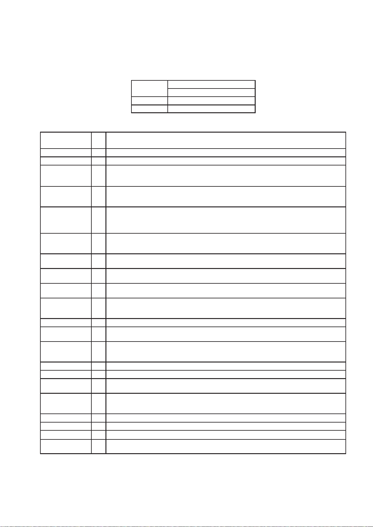
1.6 Ordering Information
PACKAGE
T
A
PLASTIC QUAD FLATPACK (PM)
0°C to 70°C TLC320AD535
–40°C to 85°C TLC320AD535I
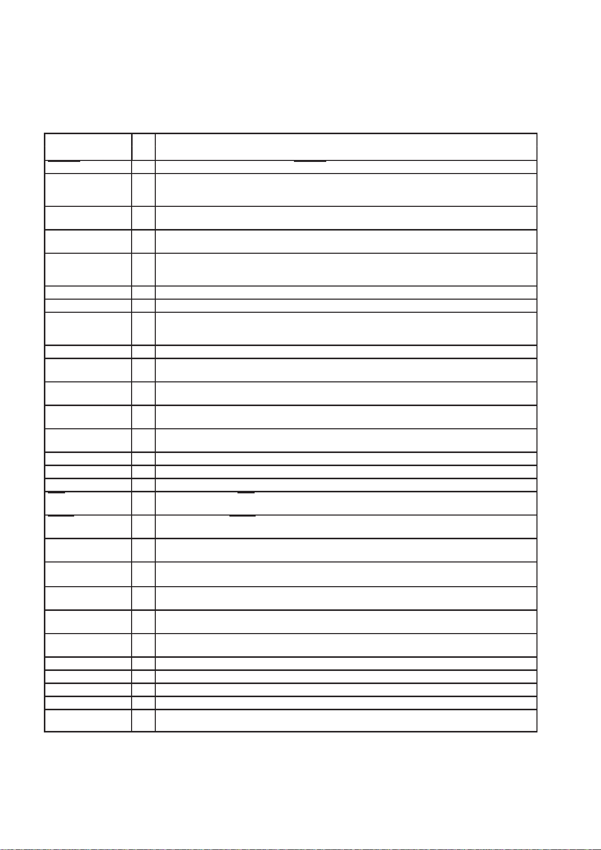
1.7 Terminal Functions
TERMINAL
NAME NO.
I/O
DESCRIPTION
DAV
DD
2 I Data channel analog power supply (5 V/3.3 V)
DAV
SS
5 I Data channel analog ground
DREFM_ADC 7 O Data channel ADC voltage reference filter output. DREFM_ADC provides low-pass filtering for the internal
bandgap reference. The optimal ceramic capacitor value is 0.1 µF, which is connected between DREFM_ADC
and DREFP_ADC. The nominal DC voltage at this terminal is 0 V.
DREFM_DAC 4 O Data channel DAC voltage reference filter output. DREFM_DAC provides low-pass filtering for the internal
bandgap reference. The optimal ceramic capacitor value is 0.1 µF, which is connected between DREFM_DAC
and DREFP_DAC. The nominal dc voltage at this terminal is 0 V.
DREFP_ADC 6 O Data channel ADC voltage reference filter output. DREFP_ADC provides low-pass filtering for the internal
bandgap reference. The optimal ceramic capacitor value is 0.1 µF, which is connected between DREFM_ADC
and DREFP_ADC. The dc voltage at this terminal is 3.375 V at 5-V DAVDD supply and 2.25 V at 3.3-V DAV
DD
supply.
DREFP_DAC 3 O Data channel DAC voltage reference filter output. DREFP_DAC provides low-pass filtering for the internal
bandgap reference. The optimal ceramic capacitor value is 0.1 µF, which is connected between DREFM_DAC
and DREFP_DAC. The dc voltage at this terminal is 3.375 V at 5-DAVDD supply and 2.25 V at 3.3-DAVDD supply.
DT_BUF 15 O Data channel buffer amp analog output. DT_BUF is programmed for 0-dB gain or is muted using the control
registers. This output is normally fed to the DTTX_IN terminal through an input resistor.
DT_DIN 26 I Data channel digital data input. DT_DIN handles DAC input data as well as control register programming
information during the data channel frame sync interval and is synchronized to DT_SCLK.
DT_DOUT 22 O Data channel digital data output. Data channel ADC output bits are transmitted during the data channel frame
sync period that is synchronized to DT_SCLK. DT_DOUT is at high impedance when DT_FS is not activated.
DT_FS 21 O Data channel serial port frame sync signal. DT_FS signals the beginning of transmit for ADC data and receiving
of DAC data in the data channel. This signal can be active high (FS high mode) or active low (FS low mode)
depending on the voltage applied to SI_SEL (See Section 4,
Serial Communications
for more details).
DT_MCLK 27 I Data channel master clock input. All of the internal clocks for the data channel are derived from this clock.
DT_REF 12 O Handset amplifier reference voltage. The voltage at this pin is set at 2.5 V for a 5-V DA VDD supply and 1.5 V for
a 3.3-V DAVDD supply. The maximum source current at this terminal is 2.5 mA.
DTRX_FB 9 O Data channel receive path amplifier feedback node. DTRX_FB connects to the output of the data channel receive
path amplifier and allows a parallel resistor/capacitor to be placed in the amplifier feedback path for setting gain
and filter poles.
DTRXM 10 I Data channel receive path amplifier analog inverting input
DTRXP 11 I Data channel receive path amplifier analog noninverting input.
DT_SCLK 25 O Data channel shift clock signal. This signal clocks serial data into DT_DIN and out of DT_DOUT during the data
channel frame-sync interval. DT_SCLK = DT_MCLK/2
DTTX_IN 14 I Data channel transmit amplifier analog inverting input. This node is normally fed by the DT_BUF output through
an input resistor. The noninverting input of the amplifier is connected internally to 2.5 V for 5 V supply and 1.5
V for 3.3 V supply.
DTTX_OUT 13 O Data channel transmit amplifier analog output
DV
DD
24 I Digital power supply (5 V/3.3 V).
DV
SS
23 I Digital ground
FILT 57 O Bandgap filter node. FILT provides decoupling of the 3.375-V bandgap reference. The optimal capacitor value
is 0.1 µF (ceramic). This node should not be used as a voltage source.
1–6
1.7 Terminal Functions (Continued)
TERMINAL
NAME NO.
I/O
DESCRIPTION
FLSH_IN 18 I External logic input. When brought low FLSH_IN enables the FLSH_OUT output.
FLSH_OUT 17 O Power output to write/erase flash EEPROM device (such as Intel 28F400B or AMD Am29F400). Outputs 5 V
(± 10%) at 45 mA maximum when FLSH_IN is brought low. FLSH_OUT does not go to a logic high state when
off. There is an internal NMOS pull down to maintain the specified voltage. An external pull down is not required.
HS_BUF 35 O Handset buffer amplifier analog output. HS_BUF can be programmed for 0-dB gain or muted using the control
registers. This output is normally fed to the HSTX_IN terminal through an input resistor.
HS_REF 38 O Handset amplifier reference voltage HS_REF is set at 2.5 V for 5-V supply and 1.5 V for 3.3-V supply. The
maximum source current at this terminal is 2.5 mA.
HSRX_FB 41 O Feedback node for handset receive path amplifier . HSRX_FB is connected to the output of the handset receive
path amplifier and allows a parallel resistor/capacitor to be placed in the amplifier feedback path for setting gain
and filter poles.
HSRXM 40 I Handset receive path amplifier analog inverting input
HSRXP 39 I Handset receive path amplifier analog noninverting input
HSTX_IN 36 I Handset transmit amplifier analog inverting input. This node is normally fed by the HSBUF output through an
input resistor. The noninverting input of the amplifier is connected internally to 2.5 V for 5 V supply and 1.5 V
for 3.3 V supply.
HSTX_OUT 37 O Handset transmit amplifier analog output
MIC_AUDIO 55 I Microphone preamplifier analog input. MIC_AUDIO can be programmed to add either 0-dB or 20-dB gain using
the control registers.
MIC_BIAS 56 O Output that provides 2.5 V/1.5 V bias for electret microphone. The maximum source current at this terminal
is 5 mA.
MONOUTM 60 O 8 Ω monitor speaker amplifier analog output. MONOUTM is set for 0-dB gain or is muted using the control
registers.
MONOUTP 62 O 8 Ω monitor speaker amplifier analog output. MONOUTP is set for 0-dB gain or is muted using the control
registers.
MV
DD
61 I Monitor amplifier supply (5 V/3.3 V)
MV
SS
59 I Monitor amplifier ground
NC All terminals marked NC should be left unconnected.
POR 20 O Power on reset signal. POR remains low while the 5-V supply at MVDD is below its threshold voltage and for
40 ms after it rises above the reset threshold.
RESET 19 I Codec device reset. RESET initializes all device internal registers to their default values. This signal is active
low.
SI_SEL 33 I Serial interface mode select. When SI_SEL is tied to DV
DD,
the serial port is in FS high mode. When SI_SEL
is tied to DVSS, the serial port is in FS low mode (See Section 4,
Serial Communications
for more details).
SPKR_LEFT 51 O Analog output from 60-Ω speaker line amplifier. SPKR_LEFT is set for 0-dB gain or is muted using the control
registers.
SPKR_RIGHT 52 O Analog output from 60-Ω speaker line amplifier . SPKR_RIGHT is set for 0-dB gain or is muted using the control
registers.
TAPI_IN 50 I Analog input to the TAPI (or sound card) preamplifier which can be programmed to add either 0 dB or 20 dB
gain via the control registers.
TAPI_OUT 49 O TAPI buffer amplifier analog output. This 600-Ω amplifier is set for 0-dB gain or is muted using the control
registers.
TEST1 54 I/O T est input/output port. TEST1 is for factory testing only and should be left unconnected.
TEST2 53 I/O T est input/output port. TEST2 is for factory testing only and should be left unconnected.
VAV
DD
48 I Voice channel analog power supply (5 V/3.3 V)
VAV
SS
45 I Voice channel analog ground
VC_DIN 28 I Voice channel digital data input. VC_DIN handles DAC input data as well as control register programming
information during the voice channel frame sync interval. VC_DIN is synchronized to VC_SCLK.

1–7
1.7 Terminal Functions (Continued)
TERMINAL
NAME NO.
I/O
DESCRIPTION
VC_DOUT 29 O Voice channel digital data output. Voice channel ADC output bits are transmitted during the voice channel frame
sync period synchronized to VC_SCLK. VC_DOUT is at high impedance when VC_FS is not activated.
VC_FS 32 O V oice channel serial port frame sync signal. VC_FS signals the beginning of transmit for ADC data and receive
of DAC data in the voice channel. This signal can be active high (FS high mode) or active low (FS low mode)
depending on the voltage applied to SI_SEL (see Section 4,
Serial Communication
for more details).
VC_MCLK 30 I Voice channel master clock input. All internal clocks for the voice channel are derived from this clock.
VC_SCLK 31 O Voice channel shift clock signal. VC_SCLK clocks serial data into VC_DIN and out of VC_DOUT during the
voice channel frame-sync interval. VC_SCLK = VC_MCLK/2
VREFM_ADC 46 O Voice channel ADC voltage reference filter output. VREFM_ADC provides low-pass filtering of the internal
bandgap reference. The optimal ceramic capacitor value is 0.1 µF , which is connected between VREFM_ADC
and VREFP_ADC. The nominal dc voltage at this terminal is 0 V.
VREFM_DAC 43 O Voice channel DAC voltage reference filter output. VREFM_DAC provides low-pass filtering of the internal
bandgap reference. The optimal ceramic capacitor value is 0.1 µF , which is connected between VREFM_DAC
and VREFP_DAC. The nominal dc voltage at this terminal is 0 V.
VREFP_ADC 47 O Voice channel ADC voltage reference filter output. VREFP_ADC provides low-pass filtering the internal
bandgap reference. The optimal ceramic capacitor value is 0.1 µF , which is connected between VREFM_ADC
and VREFP_ADC. The dc voltage at this terminal is 3.375 V with a 5-V V A VDD supply and 2.25 V with a 3.3-V
VAVDD supply.
VREFP_DAC 44 O Voice channel DAC voltage reference filter output. VREFP_DAC provides low-pass filtering the internal
bandgap reference. The optimal ceramic capacitor value is 0.1 µF , which is connected between VREFM_DAC
and VREFP_DAC. The dc voltage at this terminal is 3.375 V with a 5-V V A VDD supply and 2.25 V with a 3.3-V
VAVDD supply.
V
SS
1 I Internal substrate connection. VSS should be tied to either DAVSS or VAVSS for normal operation.
 Loading...