

TLC254, TLC254A, TLC254B, TLC254Y, TLC25L4, TLC25L4A, TLC25L4B
TLC25L4Y, TLC25M4, TLC25M4A, TLC25M4B, TLC25M4Y
LinCMOS QUAD OPERATIONAL AMPLIFIERS
SLOS003F – JUNE 1983 – REVISED AUGUST 1994
1
POST OFFICE BOX 655303 • DALLAS, TEXAS 75265
D
A-Suffix Versions Offer 5-mV V
IO
D
B-Suffix Versions Offer 2-mV V
IO
D
Wide Range of Supply Voltages
1.4 V to 16 V
D
True Single-Supply Operation
D
Common-Mode Input Voltage Includes the
Negative Rail
D
Low Noise . . . 25 nV/√Hz Typ at f = 1 kHz
(High-Bias Version)
description
The TLC254, TLC254A, TLC254B, TLC25L4,
TLC254L4A, TLC254L4B, TLC25M4, TLC25M4A
and TL25M4B are low-cost, low-power quad
operational amplifiers designed to operate with
single or dual supplies. These devices utilize the
Texas Instruments silicon gate LinCMOS
process, giving them stable input-offset voltages that are available in selected grades of 2, 5, or 10 mV
maximum, very high input impedances, and extremely low input offset and bias currents. Because the input
common-mode range extends to the negative rail and the power consumption is extremely low, this series is
ideally suited for battery-powered or energy-conserving applications. The series offers operation down to a
1.4-V supply, is stable at unity gain, and has excellent noise characteristics.
These devices have internal electrostatic-discharge (ESD) protection circuits that prevent catastrophic failures
at voltages up to 2000 V as tested under MIL-STD-883C, Method 3015.1. However, care should be exercised
in handling these devices as exposure to ESD may result in degradation of the device parametric performance.
Because of the extremely high input impedance and low input bias and offset currents, applications for these
devices include many areas that have previously been limited to BIFET and NFET product types. Any circuit
using high-impedance elements and requiring small offset errors is a good candidate for cost-effective use of
these devices. Many features associated with bipolar technology are available with LinCMOS operational
amplifiers without the power penalties of traditional bipolar devices.
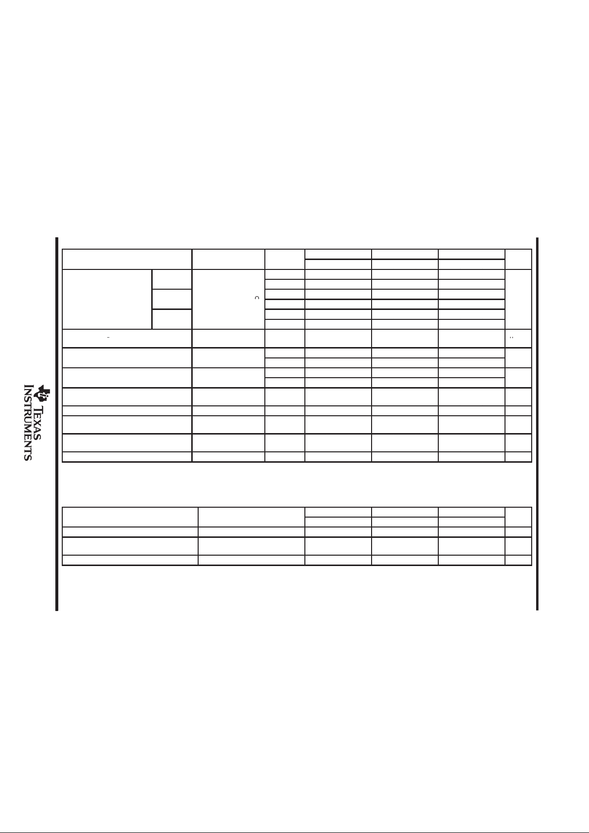
Available options
PACKAGED DEVICES
T
A
VIOmax
AT 25°C
SMALL OUTLINE
(D)
PLASTIC DIP
(N)
TSSOP
(PW)
CHIP FORM
(Y)
10 mV TLC254CD TLC254CN TLC254CPW TLC254Y
5 mV TLC254ACD TLC254ACN — —
2 mV TLC254BCD TLC254BCN — —
10 mV TLC25L4CD TLC25L4CN TLC25L4CPW TLC25L4Y
0°C to 70°C
5 mV TLC25L4ACD TLC25L4ACN — —
2 mV TLC25L2BCD TLC25L4BCN — —
10 mV TLC25M4CD TLC25M4CN TLC25M4CPW TLC25M4Y
5 mV TLC25M4ACD TLC25M4ACN — —
2 mV TLC25M4BCD TLC25M4BCN — —
The D package is available taped and reeled. Add the suffix R to the device type (e.g., TLC254CDR). Chips
are tested at 25°C.
Copyright 1994, Texas Instruments Incorporated
PRODUCTION DATA information is current as of publication date.
Products conform to specifications per the terms of Texas Instruments
standard warranty. Production processing does not necessarily include
testing of all parameters.
LinCMOS is a trademark of Texas Instruments Incorporated.
1
2
3
4
5
6
7
14
13
12
11
10
9
8
1OUT
1IN–
1IN+
V
DD
2IN+
2IN–
2OUT
4OUT
4IN–
4IN+
V
DD–
/GND
3IN+
2IN–
3OUT
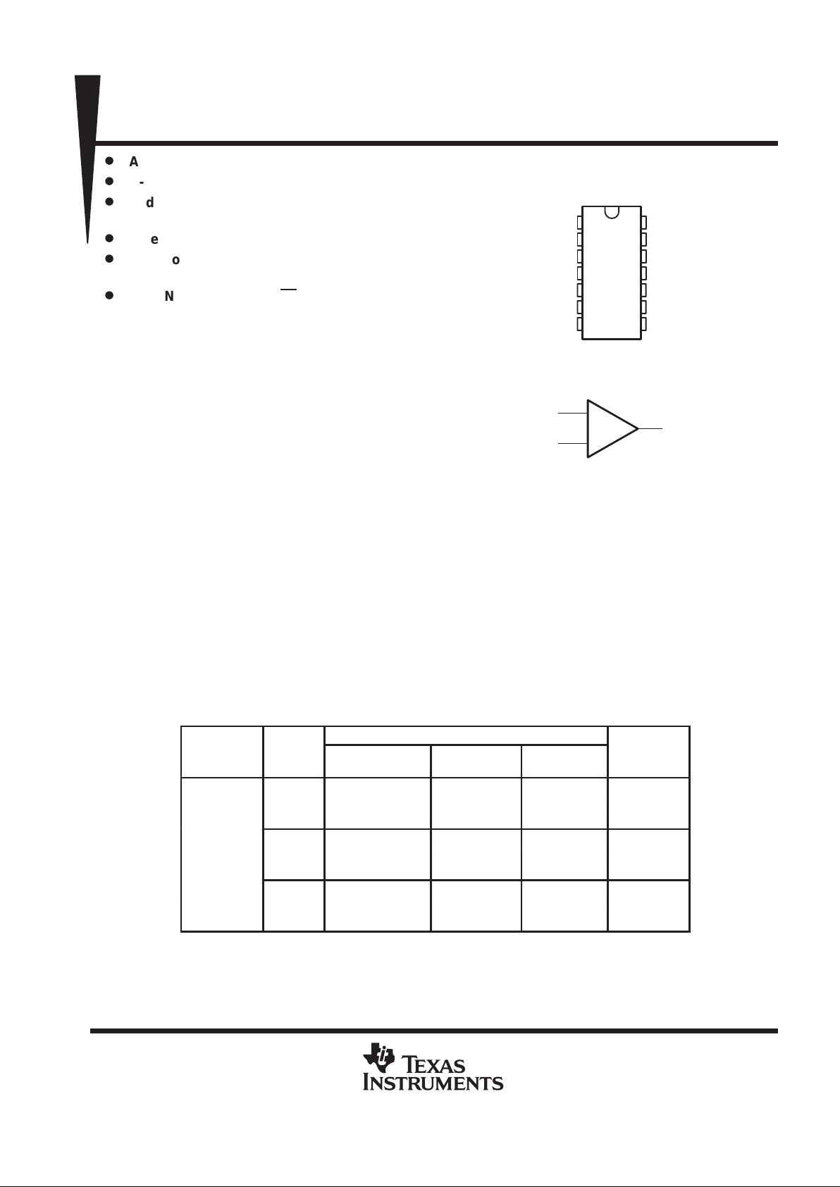
D, N, OR PW PACKAGE
(TOP VIEW)
symbol (each amplifier)
+
–
OUT
IN+
IN–
TLC254, TLC254A, TLC254B, TLC254Y, TLC25L4, TLC25L4A, TLC25L4B
TLC25L4Y, TLC25M4, TLC25M4A, TLC25M4B, TLC25M4Y
LinCMOS QUAD OPERATIONAL AMPLIFIERS
SLOS003F – JUNE 1983 – REVISED AUGUST 1994
2
POST OFFICE BOX 655303 • DALLAS, TEXAS 75265
description (continued)
General applications such as transducer interfacing, analog calculations, amplifier blocks, active filters, and
signal buffering are all easily designed with these devices. Remote and inaccessible equipment applications
are possible using their low-voltage and low-power capabilities. These devices are well suited to solve the
difficult problems associated with single-battery and solar-cell-powered applications. This series includes
devices that are characterized for the commercial temperature range and are available in 14-pin plastic dip and
the small-outline packages. The device is also available in chip form.
These devices are characterized for operation from 0°C to 70°C.
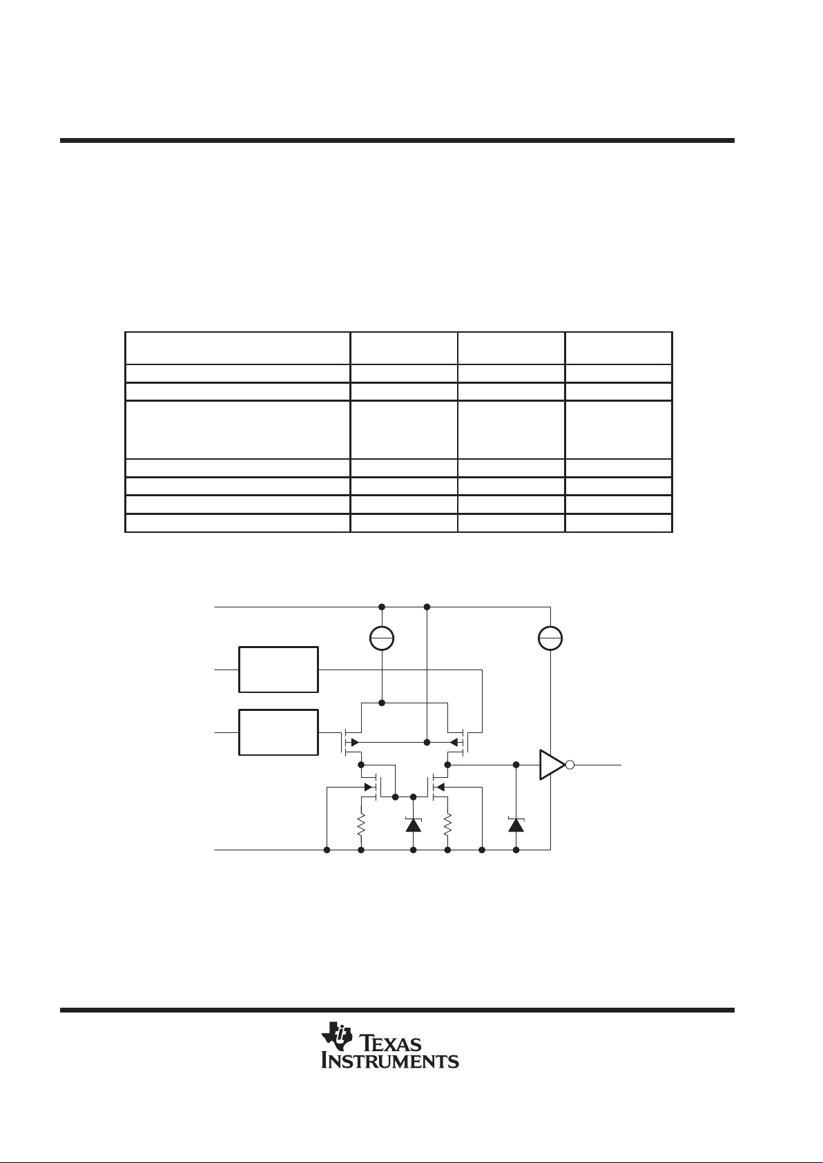
DEVICE FEATURES
PARAMETER
TLC25L4_C
(LOW BIAS)
TLC25M4_C
(MEDIUM BIAS)
TLC254_C
(HIGH BIAS)
Supply current (Typ) 40 µA 600 µA 4000 µA
Slew rate (Typ) 0.04 V/µA 0.6 V/µA 4.5 V/µA
Input offset voltage (Max)
TLC254C, TLC25L4C, TLC25M4C
TLC254AC, TLC25L4AC, TLC25M4AC
TLC254BC, TLC25L4BC, TLC25M4BC
10 mV
5 mV
2 mV
10 mV
5 mV
2 mV
10 mV
5 mV
2 mV
Offset voltage drift (Typ) 0.1 µV/month
†
0.1 µV/month
†
0.1 µV/month
†
Offset voltage temperature coefficient (T yp) 0.7 µV/°C 2 µV/°C 5 µV/°C
Input bias current (Typ) 1 pA 1 pA 1 pA
Input offset current (T yp) 1 pA 1 pA 1 pA
†
The long-term drift value applies after the first month.
equivalent schematic (each amplifier)
V
DD
IN+
IN–
V
DD–
/GND
OUT
ESD-
Protective
Network
ESD-
Protective
Network
TLC254, TLC254A, TLC254B, TLC254Y, TLC25L4, TLC25L4A, TLC25L4B
TLC25L4Y, TLC25M4, TLC25M4A, TLC25M4B, TLC25M4Y
LinCMOS QUAD OPERATIONAL AMPLIFIERS
SLOS003F – JUNE 1983 – REVISED AUGUST 1994
3
POST OFFICE BOX 655303 • DALLAS, TEXAS 75265
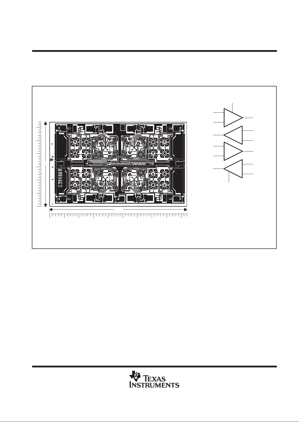
chip information
These chips, when properly assembled, display characteristics similar to the TLC25_4C. Thermal compression
or ultrasonic bonding may be used on the doped-aluminum bonding pads. Chips may be mounted with
conductive epoxy or a gold-silicon preform.
CHIP THICKNESS: 15 TYPICAL
BONDING PADS: 4 × 4 MINIMUM
TJmax = 150°C
TOLERANCES ARE ±10%.
ALL DIMENSIONS ARE IN MILS.
PIN (11) IS INTERNALLY CONNECTED
TO BACKSIDE OF CHIP.
+
–
1OUT
1IN+
1IN–
V
DD
(4)
(6)
(3)
(2)
(5)
(1)
–
+
(7)
2IN+
2IN–
2OUT
(11)
V
DD–
/GND
+
–
3OUT
3IN+
3IN–
(13)
(10)
(9)
(12)
(8)
–
+
(14)
4OUT
4IN+
4IN–
BONDING PAD ASSIGNMENTS
68
108
(14) (13) (12) (11) (10) (9) (8)
(7)
(6)(5)(5)(4)(3)(2)(1)
TLC254, TLC254A, TLC254B, TLC254Y, TLC25L4, TLC25L4A, TLC25L4B
TLC25L4Y, TLC25M4, TLC25M4A, TLC25M4B, TLC25M4Y
LinCMOS QUAD OPERATIONAL AMPLIFIERS
SLOS003F – JUNE 1983 – REVISED AUGUST 1994
4
POST OFFICE BOX 655303 • DALLAS, TEXAS 75265
absolute maximum ratings over operating free-air temperature range (unless otherwise noted)
†
Supply voltage, VDD (see Note 1) 18 V. . . . . . . . . . . . . . . . . . . . . . . . . . . . . . . . . . . . . . . . . . . . . . . . . . . . . . . . . . . .
Differential input voltage (see Note 2) ±18 V. . . . . . . . . . . . . . . . . . . . . . . . . . . . . . . . . . . . . . . . . . . . . . . . . . . . . . . .
Input voltage range (any input) –0.3 V to 18 V. . . . . . . . . . . . . . . . . . . . . . . . . . . . . . . . . . . . . . . . . . . . . . . . . . . . .
Duration of short-circuit at (or below) 25°C free-air temperature (see Note 3) unlimited. . . . . . . . . . . . . . . . . .
Continuous total dissipation See Dissipation Rating Table. . . . . . . . . . . . . . . . . . . . . . . . . . . . . . . . . . . . . . . . . . .
Operating free-air temperature range 0°C to 70°C. . . . . . . . . . . . . . . . . . . . . . . . . . . . . . . . . . . . . . . . . . . . . . . . . .
Storage temperature range –65°C to 150°C. . . . . . . . . . . . . . . . . . . . . . . . . . . . . . . . . . . . . . . . . . . . . . . . . . . . . . . .
Lead temperature 1,6 mm (1/16 inch) from case for 10 seconds 260°C. . . . . . . . . . . . . . . . . . . . . . . . . . . . . . .
†
Stresses beyond those listed under “absolute maximum ratings” may cause permanent damage to the device. These are stress ratings only, and
functional operation of the device at these or any other conditions beyond those indicated under “recommended operating conditions” is not
implied. Exposure to absolute-maximum-rated conditions for extended periods may affect device reliability.
NOTES: 1. All voltage values, except differential voltages, are with respect to V
DD–
/GND.
2. Differential voltages are at IN+, with respect to IN–.
3. The output may be shorted to either supply. Temperature and/or supply voltages must be limited to ensure the maximum dissipation
rating is not exceeded.
DISSIPATION RATING TABLE
T
≤ 25°C DERATING FACTOR T
= 70°C
PACKAGE
A
POWER RATING ABOVE TA = 25°CAPOWER RATING
D 725 mW 5.8 mW/°C 464 mW
N 1050 mW 9.2 mW/°C 736 mW
PW 700 mW 5.6 mW/°C 448 mW
recommended operating conditions
MIN MAX UNIT
Supply voltage, V
DD
1.4 16 V
VDD = 1.4 V 0 0.2
p
VDD = 5 V –0.2 4
Common-mode input voltage, V
IC
VDD = 10 V –0.2 9
V
VDD = 16 V –0.2 14
Operating free-air temperature, T
A
0 70 °C
TLC254, TLC254A, TLC254B, TLC254Y, TLC25L4, TLC25L4A, TLC25L4B
TLC25L4Y, TLC25M4, TLC25M4A, TLC25M4B, TLC25M4Y
LinCMOS QUAD OPERATIONAL AMPLIFIERS
SLOS003F – JUNE 1983 – REVISED AUGUST 1994
TM
POST OFFICE BOX 655303 DALLAS, TEXAS 75265
• 5
electrical characteristics at specified free-air temperature, VDD = 1.4 V (unless otherwise noted)
TLC254_C TLC25L4_C TLC25M4_C
PARAMETER
TEST CONDITIONS
†
T
A
MIN TYP MAX MIN TYP MAX MIN TYP MAX
UNIT
25°C 10 10 10
TLC25_4C
0°C to 70°C 12 12 12
p
25°C 5 5 5
VIOInput offset voltage
TLC25_4AC
V
O
= 0.2 V,
R
S
= 50
Ω
0°C to 70°C 6.5 6.5 6.5
mV
25°C 2 2 2
TLC25_4BC
0°C to 70°C 3 3 3
Average temperature coefficient of 25°C to
°
a
VIO
g
input offset voltage 70°C
111µV/°C
p
25°C 1 1 1
p
IIOInput offset current
V
O
= 0.2
V
0°C to 70°C 300 300 300
pA
p
25°C 1 1 1
p
IIBInput bias current
V
O
= 0.2
V
0°C to 70°C 600 600 600
pA
V
ICR
Common-mode input voltage range 25°C
0 to
0.2
0 to
0.2
0 to
0.2
V
V
OM
Peak output voltage swing
‡
VID = 100 mV 25°C 450 700 450 700 450 700 mV
A
VD
Large-signal differential voltage
amplification
VO = 100 to 300 mV,
RS = 50 Ω
25°C 10 20 20 V/mV
CMRR Common-mode rejection ratio
VO = 0.2 V,
VIC = V
ICR
min
25°C 60 77 60 77 60 77 dB
I
DD
Supply current VO = 0.2 V, No load 25°C 600 750 50 68 400 500 µA
†
All characteristics are measured under open-loop conditions with zero common-mode input voltage unless otherwise specified. Unless otherwise noted, an output load resistor is
connected from the output to ground and has the following value: for low bias, RL = 1 MΩ, for medium bias RL = 100 kΩ, and for high bias RL = 10 kΩ.
‡
The output swings to the potential of V
DD–
/GND.
operating characteristics, VDD = 1.4 V, TA = 25°C
TLC254_C TLC25L4_C TLC25M4_C
PARAMETER
TEST CONDITIONS
MIN TYP MAX MIN TYP MAX MIN TYP MAX
UNIT
SR Slew rate at unity gain See Figure 1 0.1 0.001 0.01 V/µs
B
1
Unity-gain bandwidth
AV = 40 dB,
RS = 50 Ω,
CL = 10 pF ,
See Figure 1
12 12 12 kHz
Overshoot factor See Figure 1 30% 35% 35%
TLC254, TLC254A, TLC254B, TLC254Y, TLC25L4, TLC25L4A, TLC25L4B
TLC25L4Y, TLC25M4, TLC25M4A, TLC25M4B, TLC25M4Y
LinCMOS QUAD OPERATIONAL AMPLIFIERS
SLOS003F – JUNE 1983 – REVISED AUGUST 1994
7
POST OFFICE BOX 655303 • DALLAS, TEXAS 75265
electrical characteristics at specified free-air temperature, VDD = 5 V (unless otherwise noted)
PARAMETER TEST CONDITIONS
T
†
TLC254, TLC254AC,
TLC254BC
UNIT
A
MIN TYP MAX
V
= 1.4 V, V
= 0,
25°C 1.1 10
TLC254C
O
,
RS = 50 Ω,
IC
,
RL = 10 kΩ
Full range
12
p
V
= 1.4 V, V
= 0,
25°C 0.9 5
VIOInput offset voltage
TLC254AC
O
,
RS = 50 Ω,
IC
,
RL = 10 kΩ
Full range
6.5
mV
V
= 1.4 V, V
= 0,
25°C 0.34 2
TLC254BC
O
,
RS = 50 Ω,
IC
,
RL = 10 kΩ
Full range
3
Average temperature coefficient of input 25°C to
°
α
VIO
g
offset voltage 70°C
1.8µV/°C
p
25°C 0.1
p
IIOInput offset current (see Note 4)
V
O
= 2.5 V,
V
IC
= 2.5
V
70°C 7 300
pA
p
25°C 0.6
p
IIBInput bias current (see Note 4)
V
O
=
2.5 V
,
V
IC
=
2.5 V
70°C 40 600
pA
Common-mode input voltage range
25°C
–0.2
to
4
–0.3
to
4.2
V
ICR
gg
(see Note 5)
Full range
–0.2
to
3.5
V
0°C 3 3.8
V
OH
High-level output voltage VID = 100 mV , RL = 10 kΩ
25°C
3.2 3.8
V
70°C 3 3.8
0°C 0 50
V
OL
Low-level output voltage VID = –100 mV, IOL = 0
25°C
0 50
mV
70°C 0 50
0°C 4 27
A
VD
Large-signal differential voltage
p
VO = 0.25 V to 2 V, RL = 10 kΩ
25°C
5 23
V/mV
am lification
70°C 4 20
0°C 60 84
CMRR Common-mode rejection ratio VIC = V
ICR
min
25°C 65 80
dB
70°C 60 85
0°C 60 94
k
SVR
Supply-voltage rejection ratio (∆VDD/∆VIO)VDD = 5 V to 10 V, VO = 1.4 V
25°C
65 95
dB
70°C 60 96
0°C 3.1 7.2
I
DD
Supply current (four amplifiers)
V
O
= 2.5 V,
V
IC
= 2.5 V,
25°C
2.7 6.4
mA
No load
70°C 2.3 5.2
†
Full range is 0°C to 70°C.
NOTES: 4. The typical values of input bias current and input offset current below 5 pA were determined mathematically.
5. This range also applies to each input individually.
TLC254, TLC254A, TLC254B, TLC254Y, TLC25L4, TLC25L4A, TLC25L4B
TLC25L4Y, TLC25M4, TLC25M4A, TLC25M4B, TLC25M4Y
LinCMOS QUAD OPERATIONAL AMPLIFIERS
SLOS003F – JUNE 1983 – REVISED AUGUST 1994
8
POST OFFICE BOX 655303 • DALLAS, TEXAS 75265
electrical characteristics at specified free-air temperature, VDD = 10 V (unless otherwise noted)
PARAMETER TEST CONDITIONS
T
†
TLC254C, TLC254AC,
TLC254BC
UNIT
A
MIN TYP MAX
V
= 1.4 V, V
= 0,
25°C 1.1 10
TLC254C
O
,
RS = 50 Ω,
IC
,
RL = 10 kΩ
Full range
12
p
V
= 1.4 V, V
= 0,
25°C 0.9 5
VIOInput offset voltage
TLC254AC
O
,
RS = 50 Ω,
IC
,
RL = 10 kΩ
Full range
6.5
mV
V
= 1.4 V, V
= 0,
25°C 0.39 2
TLC254BC
O
,
RS = 50 Ω,
IC
,
RL = 10 kΩ
Full range
3
Average temperature coefficient of input 25°C to
°
∝
VIO
g
offset voltage 70°C
2µV/°C
p
25°C 0.1
p
IIOInput offset current (see Note 4)
V
O
= 5 V,
V
IC
= 5
V
70°C 7 300
pA
p
25°C 0.7
p
IIBInput bias current (see Note 4)
V
O
=
5 V
,
V
IC
=
5 V
70°C 50 600
pA
Common-mode input voltage range
25°C
–0.2
to
9
–0.3
to
9.2
V
ICR
gg
(see Note 5)
Full range
–0.2
to
8.5
V
0°C 7.8 8.5
V
OH
High-level output voltage VID = 100 mV , RL = 10 kΩ
25°C
8 8.5
V
70°C 7.8 8.4
0°C 0 50
V
OL
Low-level output voltage VID = –100 mV, IOL = 0
25°C
0 50
mV
70°C 0 50
0°C 7.5 42
A
VD
Large-signal differential voltage
p
VO = 1 V to 6 V, RL = 10 kΩ
25°C
10 36
V/mV
am lification
70°C 7.5 32
0°C 60 88
CMRR Common-mode rejection ratio VIC = V
ICR
min
25°C 65 85
dB
70°C 60 88
0°C 60 94
k
SVR
Supply-voltage rejection ratio
VDD = 5 V to 10 V, VO = 1.4 V
25°C
65 95
dB
(∆VDD/∆VIO)
70°C 60 96
0°C 4.5 8.8
I
DD
Supply current (four amplifiers)
V
O
= 5 V,
V
IC
= 5 V,
25°C
3.8 8
mA
No load
70°C 3.2 6.8
†
Full range is 0°C to 70°C.
NOTES: 4. The typical values of input bias current and input offset current below 5 pA were determined mathematically .
5. This range also applies to each input individually.

TLC254, TLC254A, TLC254B, TLC254Y, TLC25L4, TLC25L4A, TLC25L4B
TLC25L4Y, TLC25M4, TLC25M4A, TLC25M4B, TLC25M4Y
LinCMOS QUAD OPERATIONAL AMPLIFIERS
SLOS003F – JUNE 1983 – REVISED AUGUST 1994
9
POST OFFICE BOX 655303 • DALLAS, TEXAS 75265
operating characteristics, VDD = 5 V
PARAMETER TEST CONDITIONS T
TLC254C, TLC254AC,
TLC254BC
UNIT
A
MIN TYP MAX
0°C 4
V
I(PP)
=
1 V
25°C 3.6
R
= 10 kΩ, C
= 20 pF,
V
I(PP)
= 1 V
70°C 3
SR
Slew rate at unity gain
L
,
See Figure 1
L
,
0°C 3.1
V/µs
V
I(PP)
= 2.5 V
25°C 2.9
()
70°C 2.5
V
n
Equivalent input noise voltage f = 1 kHz, RS = 20 Ω, See Figure 2 25°C 25
nV/√Hz
0°C 340
B
OM
Maximum output-swing bandwidth
VO = VOH,
CL = 20 pF, RL = 10 kΩ,
25°C
320
kHz
See Figure 1
70°C 260
0°C 2
B
1
Unity-gain bandwidth VI = 10 mV, CL = 20 pF, See Figure 1
25°C
1.7
MHz
70°C 1.3
0°C 47°
φ
m
Phase margin
V
I
=
10 mV
,
f
=
B
1
,
C
L
=
20 pF
,
25°C
46°
See Figure 3
70°C 43°
operating characteristics, VDD = 10 V
PARAMETER TEST CONDITIONS T
TLC254C, TLC254AC,
TLC254BC
UNIT
A
MIN TYP MAX
0°C 5.9
V
I(PP)
= 1 V
25°C 5.3
R
= 10 kΩ, C
= 20 pF,
()
70°C 4.3
SR
Slew rate at unity gain
L
,
See Figure 1
L
,
0°C 5.1
V/µs
V
I(PP)
= 5.5 V
25°C 4.6
()
70°C 3.8
V
n
Equivalent input noise voltage f = 1 kHz, RS = 20 Ω, See Figure 2 25°C 25
nV/√Hz
0°C 220
B
OM
Maximum output-swing bandwidth
VO = VOH,
CL = 20 pF, RL = 10 kΩ,
25°C
200
kHz
See Figure 1
70°C 140
0°C 2.5
B
1
Unity-gain bandwidth VI = 10 mV, CL = 20 pF, See Figure 1
25°C
2.2
MHz
70°C 1.8
0°C 50°
φ
m
Phase margin
V
I
= 10 mV,
f
=
B
1
,
C
L
= 20 pF,
25°C
49°
See Figure 3
70°C 46°

TLC254, TLC254A, TLC254B, TLC254Y, TLC25L4, TLC25L4A, TLC25L4B
TLC25L4Y, TLC25M4, TLC25M4A, TLC25M4B, TLC25M4Y
LinCMOS QUAD OPERATIONAL AMPLIFIERS
SLOS003F – JUNE 1983 – REVISED AUGUST 1994
10
POST OFFICE BOX 655303 • DALLAS, TEXAS 75265
electrical characteristics at specified free-air temperature, VDD = 5 V (unless otherwise noted)
PARAMETER TEST CONDITIONS
T
A
†
TLC25L4C
TLC25L4AC
TLC25L4BC
UNIT
MIN TYP MAX
V
= 1.4 V, V
= 0,
25°C 1.1 10
TLC25L4C
O
,
RS = 50 Ω,
IC
,
RL = 1 MΩ
Full range
12
p
V
= 1.4 V, V
= 0,
25°C 0.9 5
VIOInput offset voltage
TLC25L4AC
O
,
RS = 50 Ω,
IC
,
RL = 1 MΩ
Full range
6.5
mV
V
= 1.4 V, V
= 0,
25°C 0.24 2
TLC25L4BC
O
,
RS = 50 Ω,
IC
,
RL = 1 MΩ
Full range
3
Average temperature coefficient of input 25°C to
°
∝
VIO
g
offset voltage 70°C
1.1µV/°C
p
25°C 0.1
p
IIOInput offset current (see Note 4)
V
O
= 2.5 V,
V
IC
= 2.5
V
70°C 7 300
pA
p
25°C 0.6
p
IIBInput bias current (see Note 4)
V
O
= 2.5 V,
V
IC
= 2.5
V
70°C 40 600
pA
Common-mode input voltage range
25°C
–0.2
to
4
–0.3
to
4.2
V
V
ICR
gg
(see Note 5)
Full range
–0.2
to
3.5
V
0°C 3 4.1
V
OH
High-level output voltage VID = 100 mV , RL = 1 MΩ
25°C
3.2 4.1
V
70°C 3 4.2
0°C 0 50
V
OL
Low-level output voltage VID = –100 mV, IOL = 0
25°C
0 50
mV
70°C 0 50
0°C 50 680
A
VD
Large-signal differential voltage
p
VO = 0.25 V to 2 V, RL = 1 MΩ
25°C
50 520
V/mV
am lification
70°C 50 380
0°C 60 95
CMRR Common-mode rejection ratio VIC = V
ICR
min
25°C 65 94
dB
70°C 60 95
0°C 60 97
k
SVR
Supply-voltage rejection ratio
VDD = 5 V to 10 V, VO = 1.4 V
25°C
70 98
dB
(∆VDD/∆VIO)
70°C 60 97
0°C 48 84
I
DD
Supply current (four amplifiers)
V
O
=
2.5 V
,
V
IC
=
2.5 V
,
25°C
40 68
µA
No load
70°C 31 56
†
Full range is 0°C to 70°C.
NOTES: 4. The typical values of input bias current and input offset current below 5 pA were determined mathematically .
5. This range also applies to each input individually.

TLC254, TLC254A, TLC254B, TLC254Y, TLC25L4, TLC25L4A, TLC25L4B
TLC25L4Y, TLC25M4, TLC25M4A, TLC25M4B, TLC25M4Y
LinCMOS QUAD OPERATIONAL AMPLIFIERS
SLOS003F – JUNE 1983 – REVISED AUGUST 1994
11
POST OFFICE BOX 655303 • DALLAS, TEXAS 75265
electrical characteristics at specified free-air temperature, VDD = 10 V (unless otherwise noted)
PARAMETER TEST CONDITIONS
T
A
†
TLC25L4C
TLC25L4AC
TLC25L4BC
UNIT
MIN TYP MAX
V
= 1.4 V, V
= 0,
25°C 1.1 10
TLC25L4C
O
,
RS = 50 Ω,
IC
,
RL = 1 MΩ
Full range
12
p
V
= 1.4 V, V
= 0,
25°C 0.9 5
VIOInput offset voltage
TLC25L4AC
O
,
RS = 50 Ω,
IC
,
RL = 1 MΩ
Full range
6.5
mV
V
= 1.4 V, V
= 0,
25°C 0.26 2
TLC25L4BC
O
,
RS = 50 Ω,
IC
,
RL = 1 MΩ
Full range
3
Average temperature coefficient of 25°C to
°
α
VIO
g
input offset voltage 70°C
1µV/°C
p
25°C 0.1
p
IIOInput offset current (see Note 4)
V
O
= 5 V,
V
IC
= 5
V
70°C 7 300
pA
p
25°C 0.7
p
IIBInput bias current (see Note 4)
V
O
= 5 V,
V
IC
=.5
V
70°C 50 600
pA
Common-mode input voltage range (see
25°C
–0.2
to
9
–0.3
to
9.2
V
V
ICR
gg(
Note 5)
Full range
–0.2
to
8.5
V
0°C 7.8 8.9
V
OH
High-level output voltage VID = 100 mV , RL = 1 MΩ
25°C
8 8.9
V
70°C 7.8 8.9
0°C 0 50
V
OL
Low-level output voltage VID = –100 mV, IOL = 0
25°C
0 50
mV
70°C 0 50
0°C 50 1025
A
VD
Large-signal differential voltage
p
VO = 1 V to 6 V, RL = 1 MΩ
25°C
50 870
V/mV
am lification
70°C 50 660
0°C 60 97
CMRR Common-mode rejection ratio VIC = V
ICR
min
25°C 65 97
dB
70°C 60 97
0°C 60 97
k
SVR
Supply-voltage rejection ratio
VDD = 5 V to 10 V, VO = 1.4 V
25°C
70 97
dB
(∆VDD/∆VIO)
70°C 60 98
0°C 72 132
I
DD
Supply current (four amplifiers)
V
O
= 5 V,
V
IC
= 5 V,
25°C
57 92
µA
No load
70°C 44 80
†
Full range is 0°C to 70°C.
NOTES: 4. The typical values of input bias current and input offset current below 5 pA were determined mathematically .
5. This range also applies to each input individually.

TLC254, TLC254A, TLC254B, TLC254Y, TLC25L4, TLC25L4A, TLC25L4B
TLC25L4Y, TLC25M4, TLC25M4A, TLC25M4B, TLC25M4Y
LinCMOS QUAD OPERATIONAL AMPLIFIERS
SLOS003F – JUNE 1983 – REVISED AUGUST 1994
12
POST OFFICE BOX 655303 • DALLAS, TEXAS 75265
operating characteristics, VDD = 5 V
PARAMETER TEST CONDITIONS T
A
TLC25L4C
TLC25L4AC
TLC25L4BC
UNIT
MIN TYP MAX
0°C 0.04
V
I(PP)
= 1 V
25°C 0.03
R
= 1 MΩ, C
= 20 pF,
()
70°C 0.03
SR
Slew rate at unity gain
L
,
See Figure 1
L
,
0°C 0.03
V/µs
V
I(PP)
= 2.5 V
25°C 0.03
()
70°C 0.02
V
n
Equivalent input noise voltage f = 1 kHz, RS = 20 Ω, See Figure 2 25°C 70
nV/√Hz
0°C 6
B
OM
Maximum output-swing bandwidth
VO = VOH,
CL = 20 pF, RL = 1 MΩ,
25°C
5
kHz
See Figure 1
70°C 4.5
0°C 100
B
1
Unity-gain bandwidth VI = 10 mV, CL = 20 pF, See Figure 1
25°C
85
kHz
70°C 65
0°C 36°
φ
m
Phase margin
V
I
= 10 mV,
f
=
B1,C
L
= 20 pF,
25°C
34°
See Figure 3
70°C 30°
operating characteristics, VDD = 10 V
PARAMETER TEST CONDITIONS T
A
TLC25L4C
TLC25L4AC
TLC25L4BC
UNIT
MIN TYP MAX
0°C 0.05
V
I(PP)
= 1 V
25°C 0.05
R
= 1 MΩ, C
= 20 pF,
()
70°C 0.04
SR
Slew rate at unity gain
L
,
See Figure 1
L
,
0°C 0.05
V/µs
V
I(PP)
= 5.5 V
25°C 0.04
()
70°C 0.04
V
n
Equivalent input noise voltage f = 1 kHz, RS = 20 Ω, See Figure 2 25°C 70
nV/√Hz
0°C 1.3
B
OM
Maximum output-swing bandwidth
VO = VOH,
CL = 20 pF, RL = 1 MΩ,
25°C
1
kHz
See Figure 1
70°C 0.9
0°C 125
B
1
Unity-gain bandwidth VI = 10 mV, CL = 20 pF, See Figure 1
25°C
110
kHz
70°C 90
0°C 40°
φ
m
Phase margin
V
I
=
10 mV
,
f
=
B
1
,
C
L
=
20 pF
,
25°C
38°
See Figure 3
70°C 34°

TLC254, TLC254A, TLC254B, TLC254Y, TLC25L4, TLC25L4A, TLC25L4B
TLC25L4Y, TLC25M4, TLC25M4A, TLC25M4B, TLC25M4Y
LinCMOS QUAD OPERATIONAL AMPLIFIERS
SLOS003F – JUNE 1983 – REVISED AUGUST 1994
13
POST OFFICE BOX 655303 • DALLAS, TEXAS 75265
electrical characteristics at specified free-air temperature, VDD = 5 V (unless otherwise noted)
PARAMETER TEST CONDITIONS
T
A
†
TLC25M4C
TLC25M4AC
TLC25M4BC
UNIT
MIN TYP MAX
V
= 1.4 V, V
= 0,
25°C 1.1 10
TLC25M4C
O
,
RS = 50 Ω,
IC
,
RL = 100 kΩ
Full range
12
p
V
= 1.4 V, V
= 0,
25°C 0.9 5
VIOInput offset voltage
TLC25M4AC
O
,
RS = 50 Ω,
IC
,
RL = 100 kΩ
Full range
6.5
mV
V
= 1.4 V, V
= 0,
25°C 0.25 2
TLC25M4BC
O
,
RS = 50 Ω,
IC
,
RL = 100 kΩ
Full range
3
Average temperature coefficient of 25°C to
°
∝
VIO
g
input offset voltage 70°C
1.7µV/°C
p
25°C 0.1
p
IIOInput offset current (see Note 4)
V
O
= 2.5 V,
V
IC
= 2.5
V
70°C 7 300
pA
p
25°C 0.6
p
IIBInput bias current (see Note 4)
V
O
= 2.5 V,
V
IC
= 2.5
V
70°C 40 600
pA
Common-mode input voltage range
25°C
–0.2
t0
4
–0.3
to
4.2
V
V
ICR
gg
(see Note 5)
Full range
–0.2
to
3.5
V
0°C 3 3.9
V
OH
High-level output voltage VID = 100 mV , RL = 100 kΩ
25°C
3.2 3.9
V
70°C 3 4
0°C 0 50
V
OL
Low-level output voltage VID = –100 mV, IOL = 0
25°C
0 50
mV
70°C 0 50
0°C 15 200
A
VD
Large-signal differential voltage
p
VO = 0.25 V to 2 V, RL = 100 kΩ
25°C
25 170
V/mV
am lification
70°C 15 140
0°C 60 91
CMRR Common-mode rejection ratio VIC = V
ICR
min
25°C 65 91
dB
70°C 60 92
0°C 60 92
k
SVR
Supply-voltage rejection ratio
VDD = 5 V to 10 V, VO = 1.4 V
25°C
70 93
dB
(∆VDD/∆VIO)
70°C 60 94
0°C 500 1280
I
DD
Supply current (four amplifiers)
V
O
= 2.5 V,
V
IC
= 2.5 V,
25°C
420 1120
µA
No load
70°C 340 880
†
Full range is 0°C to 70°C.
NOTES: 4. The typical values of input bias current and input offset current below 5 pA were determined mathematically .
5. This range also applies to each input individually.

TLC254, TLC254A, TLC254B, TLC254Y, TLC25L4, TLC25L4A, TLC25L4B
TLC25L4Y, TLC25M4, TLC25M4A, TLC25M4B, TLC25M4Y
LinCMOS QUAD OPERATIONAL AMPLIFIERS
SLOS003F – JUNE 1983 – REVISED AUGUST 1994
14
POST OFFICE BOX 655303 • DALLAS, TEXAS 75265
electrical characteristics at specified free-air temperature, VDD = 10 V (unless otherwise noted)
PARAMETER TEST CONDITIONS
T
A
†
TLC25M4C
TLC25M4AC
TLC25M4BC
UNIT
MIN TYP MAX
V
= 1.4 V, V
= 0,
25°C 1.1 10
TLC25M4C
O
,
RS = 50 Ω,
IC
,
RL = 100 kΩ
Full range
12
p
V
= 1.4 V, V
= 0,
25°C 0.9 5
VIOInput offset voltage
TLC25M4AC
O
,
RS = 50 Ω,
IC
,
RL = 100 kΩ
Full range
6.5
mV
V
= 1.4 V, V
= 0,
25°C 0.26 2
TLC25M4BC
O
,
RS = 50 Ω,
IC
,
RL = 100 kΩ
Full range
3
Average temperature coefficient of input 25°C to
°
α
VIO
g
offset voltage 70°C
2.1µV/°C
p
25°C 0.1
p
IIOInput offset current (see Note 4)
V
O
= 5 V,
V
IC
= 5
V
70°C 7 300
pA
p
25°C 0.7
p
IIBInput bias current (see Note 4)
V
O
= 5 V,
V
IC
= 5
V
70°C 50 600
pA
Common-mode input voltage range (see
25°C
–0.2
to
9
–0.3
to
9.2
V
V
ICR
gg(
Note 5)
Full range
–0.2
to
8.5
V
0°C 7.8 8.7
V
OH
High-level output voltage VID = 100 mV , RL = 100 kΩ
25°C
8 8.7
V
70°C 7.8 8.7
0°C 0 50
V
OL
Low-level output voltage VID = –100 mV, IOL = 0
25°C
0 50
mV
70°C 0 50
0°C 15 320
A
VD
Large-signal differential voltage
p
VO = 1 V to 6 V, RL = 100 kΩ
25°C
25 275
V/mV
am lification
70°C 15 230
0°C 60 94
CMRR Common-mode rejection ratio VIC = V
ICR
min
25°C 65 94
dB
70°C 60 94
0°C 60 92
k
SVR
Supply-voltage rejection ratio (∆VDD/∆VIO)VDD = 5 V to 10 V, VO = 1.4 V
25°C
70 93
dB
70°C 60 94
0°C 690 1600
I
DD
Supply current (four amplifiers)
V
O
= 5 V,
V
IC
= 5 V,
25°C
570 1200
µA
No load
70°C 440 1120
†
Full range is 0°C to 70°C.
NOTES: 4. The typical values of input bias current and input offset current below 5 pA were determined mathematically .
5. This range also applies to each input individually.

TLC254, TLC254A, TLC254B, TLC254Y, TLC25L4, TLC25L4A, TLC25L4B
TLC25L4Y, TLC25M4, TLC25M4A, TLC25M4B, TLC25M4Y
LinCMOS QUAD OPERATIONAL AMPLIFIERS
SLOS003F – JUNE 1983 – REVISED AUGUST 1994
15
POST OFFICE BOX 655303 • DALLAS, TEXAS 75265
operating characteristics, VDD = 5 V
PARAMETER TEST CONDITIONS T
A
TLC25M4C
TLC25M4AC
TLC25M4BC
UNIT
MIN TYP MAX
0°C 0.46 V/µs
V
I(PP)
= 1 V
25°C 0.43 V/µs
R
= 100 kΩ, C
= 20 pF,
70°C 0.36
SR
Slew rate at unity gain
L
,
See Figure 1
L
,
0°C 0.43
V
I(PP)
= 2.5 V
25°C 0.40
V/µs
()
70°C 0.34
V
n
Equivalent input noise voltage f = 1 kHz, RS = 20 Ω, See Figure 2 25°C 32
nV/√Hz
0°C 60
B
OM
Maximum output-swing bandwidth
VO = VOH,
CL = 20 pF, RL = 100 kΩ,
25°C
55
kHz
See Figure 1
70°C 50
0°C 610
B
1
Unity-gain bandwidth VI = 10 mV, CL = 20 pF, See Figure 1
25°C
525
kHz
70°C 400
0°C 41°
φ
m
Phase margin
V
I
= 10 mV,
f
=
B1,C
L
= 20 pF,
25°C
40°
See Figure 3
70°C 39°
operating characteristics, VDD = 10 V
PARAMETER TEST CONDITIONS T
A
TLC25M4C
TLC25M4AC
TLC25M4BC
UNIT
MIN TYP MAX
0°C 0.67
V
I(PP)
= 1 V
25°C 0.62
R
= 100 kΩ, C
= 20 pF,
()
70°C 0.51
SR
Slew rate at unity gain
L
,
See Figure 1
L
,
0°C 0.61
V/µs
V
I(PP)
= 5.5 V
25°C 0.56
()
70°C 0.46
V
n
Equivalent input noise voltage f = 1 kHz, RS = 20 Ω, See Figure 2 25°C 32
nV/√Hz
0°C 40
B
OM
Maximum output-swing bandwidth
VO = VOH,
CL = 20 pF, RL = 100 kΩ,
25°C
35
kHz
See Figure 1
70°C 30
0°C 710
B
1
Unity-gain bandwidth VI = 10 mV, CL = 20 pF, See Figure 1
25°C
635
kHz
70°C 510
0°C 44°
φ
m
Phase margin
V
I
=
10 mV
,
f
=
B
1
,
C
L
=
20 pF
,
25°C
43°
See Figure 3
70°C 42°

TLC254, TLC254A, TLC254B, TLC254Y, TLC25L4, TLC25L4A, TLC25L4B
TLC25L4Y, TLC25M4, TLC25M4A, TLC25M4B, TLC25M4Y
LinCMOS QUAD OPERATIONAL AMPLIFIERS
SLOS003F – JUNE 1983 – REVISED AUGUST 1994
16
POST OFFICE BOX 655303 • DALLAS, TEXAS 75265
electrical characteristics, VDD = 5 V, TA = 25°C (unless otherwise noted)
TEST
TLC254Y TLC25L4Y TLC25M4Y
PARAMETER
CONDITIONS
MIN TYP MAX MIN TYP MAX MIN TYP MAX
UNIT
V
IO
Input offset voltage
VO = 1.4 V,
VIC = 0 V,
RS = 50 Ω,
See Note 6
1.1 10 1.1 10 1.1 10 mV
α
VIO
Average temperature
coefficient of input
offset voltage
1.8 1.1 1.7 µV/°C
I
IO
Input offset current
(see Note 4)
VO = VDD/2,
VIC = VDD/2
0.1 0.1 0.1 pA
I
IB
Input bias current
(see Note 4)
VO = VDD/2,
VIC = VDD/2
0.6 0.6 0.6 pA
V
ICR
Common-mode input
voltage range
(see Note 5)
–0.2
to
4
–0.3
to
4.2
–0.2
to
4
–0.3
to
4.2
–0.2
to
4
–0.3
to
4.2
V
V
OH
High-level output
voltage
VID = 100 mV ,
RL = 100 kΩ
3.2 3.8 3.2 4.1 3.2 3.9 V
V
OL
Low-level output voltage
VID = –100 mV,
IOL = 0
0 50 0 50 0 50 mV
A
VD
Large-signal differential
voltage amplification
VO = 0.25 V ,
See Note 6
5 23 50 520 25 170 V/mV
CMRR
Common-mode rejection
ratio
VIC = V
ICR
min 65 80 65 94 65 91 dB
k
SVR
Supply-voltage rejection
ratio (∆VDD/∆VIO)
VDD = 5 V to 10 V,
VO = 1.4 V
65 95 70 97 70 93 dB
I
DD
Supply current
VO = VDD/2,
VIC = VDD/2,
No load
2.7 6.4 0.04 0.068 0.42 1.12 mA
NOTES: 4. The typical values of input bias current and input offset current below 5 pA were determined mathematically.
5. This range also applies to each input individually.
6. For low-bias mode, RL = 1 MΩ, for medium-bias mode, RL = 100 kΩ, and for high-bias mode, RL = 10 kΩ.
operating characteristics, VDD = 5 V, TA = 25°C
TLC254Y TLC25L4Y TLC25M4Y
PARAMETER
TEST CONDITIONS
MIN TYP MAX MIN TYP MAX MIN TYP MAX
UNIT
Slew rate at C
= 20 pF,
V
I(PP)
= 1 V 3.6 0.03 0.43
SR
unity gain
L
,
See Note 6
V
I(PP)
= 2.5 V 2.9 0.03 0.40
V/µs
V
n
Equivalent
input noise
voltage
f = 1 kHz, RS = 20 Ω 2.5 70 32
nV/√Hz
B
OM
Maximum
output-swing
bandwidth
VO = VOH,
RL = 10 kΩ
CL = 20 pF,
320 5 55 kHz
B
1
Unity-gain
bandwidth
VI = 10 mV, CL = 20 pF 1.7 0.085 0.525 MHz
φ
m
Phase margin
f = B1,
CL = 20 pF
VI = 10 mV,
46° 34° 40°
NOTE 6: For low-bias mode, RL = 1 MΩ, for medium-bias mode, RL = 100 kΩ, and for high-bias mode, RL = 10 kΩ.

TLC254, TLC254A, TLC254B, TLC254Y, TLC25L4, TLC25L4A, TLC25L4B
TLC25L4Y, TLC25M4, TLC25M4A, TLC25M4B, TLC25M4Y
LinCMOS QUAD OPERATIONAL AMPLIFIERS
SLOS003F – JUNE 1983 – REVISED AUGUST 1994
17
POST OFFICE BOX 655303 • DALLAS, TEXAS 75265
PARAMETER MEASUREMENT INFORMATION
single-supply versus split-supply test circuits
Because the TLC25_4, TLC25_4A, and TLC25_4B are optimized for single-supply operation, circuit
configurations used for the various tests often present some inconvenience since the input signal, in many
cases, must be offset from ground. This inconvenience can be avoided by testing the device with split supplies
and the output load tied to the negative rail. A comparison of single-supply versus split-supply test circuits is
shown below. The use of either circuit gives the same result.
–
+
–
+
V
DD
V
I
C
L
R
L
V
O
V
DD+
V
DD–
V
I
V
O
C
L
R
L
(a) SINGLE-SUPPL Y
(b) SPLIT-SUPPLY
Figure 1. Unity-Gain Amplifier
–
+
–
+
1/2 V
DD
V
DD
20 Ω
20 Ω
2 kΩ
V
DD–
V
O
V
O
20 Ω
20 Ω
(a) SINGLE-SUPPL Y
2 kΩ
V
DD+
(b) SPLIT-SUPPLY
Figure 2. Noise-Test Circuit
–
+
–
+
10 kΩ
1/2 V
DD
100Ω
V
O
V
DD
V
I
V
I
100Ω
(a) SINGLE-SUPPL Y (b) SPLIT-SUPPLY
10 kΩ
V
DD+
V
DD–
C
L
C
L
V
O
Figure 3. Gain-of-100 Inverting Amplifier

TLC254, TLC254A, TLC254B, TLC254Y, TLC25L4, TLC25L4A, TLC25L4B
TLC25L4Y, TLC25M4, TLC25M4A, TLC25M4B, TLC25M4Y
LinCMOS QUAD OPERATIONAL AMPLIFIERS
SLOS003F – JUNE 1983 – REVISED AUGUST 1994
18
POST OFFICE BOX 655303 • DALLAS, TEXAS 75265
TYPICAL CHARACTERISTICS
Table of Graphs
FIGURE
pp
vs Supply voltage 4
IDDSupply current
yg
vs Free-air temperature 5
Low bias vs Frequency 6
A
VD
Large-signal differential voltage amplification
Medium bias
vs Frequency 7
High bias vs Frequency 8
Low bias vs Frequency 6
Phase shift
Medium bias
vs Frequency 7
High bias vs Frequency 8
Figure 4
100
0
024681012
1000
10000
14 16
10
ICC – Supply Current – xA
DD
I
Aµ
18 20
VDD – Supply Voltage – V
SUPPLY CURRENT
vs
SUPPLY VOLTAGE
VO = VIC = 0.2 V
DD
No Load
TA = 25°C
High-Bias Versions
Medium-Bias Versions
Low-Bias Versions
Figure 5
100
0
0 102030405060
1000
10000
70 80
10
ICC – Supply Current – xA
DD
I
Aµ
TA – Free-Air Temperature – °C
SUPPLY CURRENT
vs
FREE-AIR TEMPERATURE
VDD = 10 V
VIC = 0
VO = 2 V
No Load
High-Bias Versions
Medium-Bias Versions
Low-Bias Versions

TLC254, TLC254A, TLC254B, TLC254Y, TLC25L4, TLC25L4A, TLC25L4B
TLC25L4Y, TLC25M4, TLC25M4A, TLC25M4B, TLC25M4Y
LinCMOS QUAD OPERATIONAL AMPLIFIERS
SLOS003F – JUNE 1983 – REVISED AUGUST 1994
19
POST OFFICE BOX 655303 • DALLAS, TEXAS 75265
TYPICAL CHARACTERISTICS
0.1 1 10 100 10 k 100 k
Phase Shift
0°
30°
60°
90°
120°
150°
10
6
10
5
10
4
10
3
10
2
10
1
1
AVD (left scale)
Phase Shift
(right scale)
10
7
0.1
VDD = 10 V
RL = 1 MΩ
TA = 25°C
180°
LOW-BIAS LARGE-SIGNAL DIFFERENTIAL
VOLTAGE AMPLIFICATION AND PHASE SHIFT
vs
FREQUENCY
Frequency – Hz
1 k
AVD – Low-Bias Large-Signal Differential
A
VD
Voltage Amplification
Figure 6
1 10 100 1 k 10 k 100 k 1 M
Frequency – Hz
Phase Shift
0°
30°
60°
90°
120°
150°
10
6
10
5
10
4
10
3
10
2
10
1
1
AVD (left scale)
Phase Shift
(right scale)
10
7
0.1
VDD = 10 V
RL = 100 kΩ
TA = 25°C
180°
MEDIUM-BIAS LARGE-SIGNAL
DIFFERENTIAL VOLTAGE AMPLIFICATION
AND PHASE SHIFT
vs
FREQUENCY
AVD – Medium-Bias Large-Signal Differential
A
VD
Voltage Amplification
Figure 7

TLC254, TLC254A, TLC254B, TLC254Y, TLC25L4, TLC25L4A, TLC25L4B
TLC25L4Y, TLC25M4, TLC25M4A, TLC25M4B, TLC25M4Y
LinCMOS QUAD OPERATIONAL AMPLIFIERS
SLOS003F – JUNE 1983 – REVISED AUGUST 1994
20
POST OFFICE BOX 655303 • DALLAS, TEXAS 75265
TYPICAL CHARACTERISTICS
Phase Shift
0°
30°
60°
90°
120°
150°
10
6
10
5
10
4
10
3
10
2
10
1
1
AVD (left scale)
Phase Shift (right scale)
10
7
0.1
VDD = 10 V
RL = 10 kΩ
TA = 25°C
180°
HIGH-BIAS LARGE-SIGNAL
DIFFERENTIAL VOLTAGE AMPLIFICATION
AND PHASE SHIFT
vs
FREQUENCY
10 100 1 k 10 k 100 k 1 M 10 M
Frequency – Hz
AVD – High-Bias Large-Signal Differential
A
VD
Voltage Amplification
Figure 8

TLC254, TLC254A, TLC254B, TLC254Y, TLC25L4, TLC25L4A, TLC25L4B
TLC25L4Y, TLC25M4, TLC25M4A, TLC25M4B, TLC25M4Y
LinCMOS QUAD OPERATIONAL AMPLIFIERS
SLOS003F – JUNE 1983 – REVISED AUGUST 1994
21
POST OFFICE BOX 655303 • DALLAS, TEXAS 75265
APPLICATION INFORMATION
latch-up avoidance
Junction-isolated CMOS circuits have an inherent parasitic PNPN structure that can function as an SCR. Under
certain conditions, this SCR may be triggered into a low-impedance state, resulting in excessive supply current.
To avoid such conditions, no voltage greater than 0.3 V beyond the supply rails should be applied to any pin.
In general, the operational amplifiers supplies should be established simultaneously with, or before, application
of any input signals.
output stage considerations
The amplifier’s output stage consists of a source-follower-connected pullup transistor and an open-drain
pulldown transistor. The high-level output voltage (VOH) is virtually independent of the IDD selection and
increases with higher values of VDD and reduced output loading. The low-level output voltage (VOL) decreases
with reduced output current and higher input common-mode voltage. With no load, VOL is essentially equal to
the potential of V
DD–
/GND.
supply configurations
Even though the TLC25_4C series is are characterized for single-supply operation, they can be used effectively
in a split-supply configuration if the input common-mode voltage (V
ICR
), output swing (VOL and VOH), and supply
voltage limits are not exceeded.
circuit layout precautions
Whenever extremely high circuit impedances are used, care must be exercised in layout, construction, board
cleanliness, and supply filtering to avoid hum and noise pickup as well as excessive dc leakages.

IMPORTANT NOTICE
T exas Instruments and its subsidiaries (TI) reserve the right to make changes to their products or to discontinue
any product or service without notice, and advise customers to obtain the latest version of relevant information
to verify, before placing orders, that information being relied on is current and complete. All products are sold
subject to the terms and conditions of sale supplied at the time of order acknowledgement, including those
pertaining to warranty, patent infringement, and limitation of liability.
TI warrants performance of its semiconductor products to the specifications applicable at the time of sale in
accordance with TI’s standard warranty. Testing and other quality control techniques are utilized to the extent
TI deems necessary to support this warranty. Specific testing of all parameters of each device is not necessarily
performed, except those mandated by government requirements.
CERT AIN APPLICATIONS USING SEMICONDUCTOR PRODUCTS MAY INVOLVE POTENTIAL RISKS OF
DEATH, PERSONAL INJURY, OR SEVERE PROPERTY OR ENVIRONMENTAL DAMAGE (“CRITICAL
APPLICATIONS”). TI SEMICONDUCTOR PRODUCTS ARE NOT DESIGNED, AUTHORIZED, OR
WARRANTED TO BE SUITABLE FOR USE IN LIFE-SUPPORT DEVICES OR SYSTEMS OR OTHER
CRITICAL APPLICATIONS. INCLUSION OF TI PRODUCTS IN SUCH APPLICA TIONS IS UNDERSTOOD T O
BE FULLY AT THE CUSTOMER’S RISK.
In order to minimize risks associated with the customer’s applications, adequate design and operating
safeguards must be provided by the customer to minimize inherent or procedural hazards.
TI assumes no liability for applications assistance or customer product design. TI does not warrant or represent
that any license, either express or implied, is granted under any patent right, copyright, mask work right, or other
intellectual property right of TI covering or relating to any combination, machine, or process in which such
semiconductor products or services might be or are used. TI’s publication of information regarding any third
party’s products or services does not constitute TI’s approval, warranty or endorsement thereof.
Copyright 2000, Texas Instruments Incorporated
 Loading...