

0°C to 125°C
查询TL750M供应商
D
Very Low Dropout Voltage, Less Than 0.6 V
at 750 mA
D
Low Quiescent Current
D
TTL- and CMOS-Compatible Enable on
TL751M Series
description
The TL750M and TL751M series are low-dropout positive voltage regulators specifically designed for
battery-powered systems. The TL750M and TL751M series incorporate onboard overvoltage and
current-limiting protection circuitry to protect the devices and the regulated system. Both series are fully
protected against 60-V load-dump and reverse-battery conditions. Extremely low quiescent current, even
during full-load conditions, makes the TL750M and TL751M series ideal for standby power systems.
The TL750M and TL751M series offers 5-V, 8-V, 10-V , and 12-V options. The TL751M series has the addition
of an enable (ENABLE) input. The ENABLE input gives the designer complete control over power up, allowing
sequential power up or emergency shutdown. When ENABLE
high-impedance state. The ENABLE input is TTL- and CMOS-compatible.
The TL750MxxC and TL751MxxC are characterized for operation over the virtual junction temperature range
0°C to 125°C.
TL750M, TL751M SERIES
LOW-DROPOUT VOLTAGE REGULATORS
SLVS021H – JANUARY 1988 – REVISED JANUAR Y 2000
D
60-V Load-Dump Protection
D
Overvoltage Protection
D
Internal Thermal Overload Protection
D
Internal Overcurrent-Limiting Circuitry
is high, the regulator output is placed in the
AVAILABLE OPTIONS
PACKAGED DEVICES
V
O
T
J
°
The KTE and KTG packages are available taped and reeled. The KTP is only available taped and reeled. Add the suffix R to device
type (e.g., TL750M05CKTER). Chip forms are tested at 25°C.
TYP
(V)
5 TL750M05CKC TL750M05CKTE TL751M05CKTG TL750M05CKTPR TL750M05Y
°
8 TL750M08CKC TL750M08CKTE TL751M08CKTG TL750M08CKTPR TL750M08Y
10 TL750M10CKC TL750M10CKTE TL751M10CKTG TL750M10CKTPR TL750M10Y
12 TL750M12CKC TL750M12CKTE TL751M12CKTG TL750M12CKTPR TL750M12Y
HEAT-SINK
MOUNTED
(3-PIN)
(KC)
PLASTIC
FLANGE MOUNT
(KTE)
PLASTIC
FLANGE MOUNT
(KTG)
PLASTIC
FLANGE MOUNT
(KTP)
CHIP
FORM
(Y)
Please be aware that an important notice concerning availability, standard warranty, and use in critical applications of
Texas Instruments semiconductor products and disclaimers thereto appears at the end of this data sheet.
PRODUCTION DATA information is current as of publication date.
Products conform to specifications per the terms of Texas Instruments
standard warranty. Production processing does not necessarily include
testing of all parameters.
POST OFFICE BOX 655303 • DALLAS, TEXAS 75265
Copyright 2000, Texas Instruments Incorporated
1
TL750M, TL751M SERIES
LOW-DROPOUT VOLTAGE REGULATORS
SLVS021H – JANUARY 1988 – REVISED JANUAR Y 2000
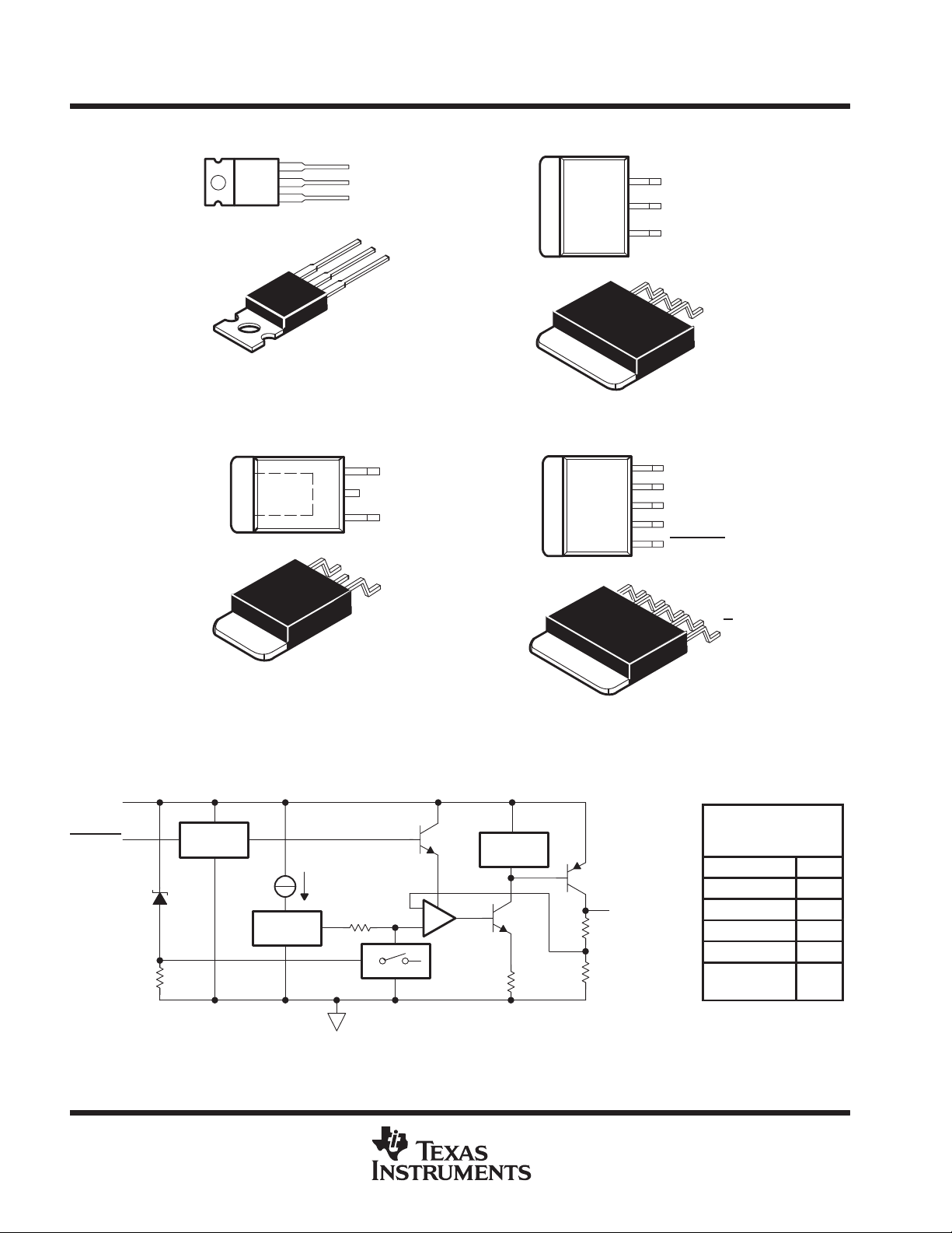
TL750M ...KC PACKAGE
(TOP VIEW)
TO-220AB
†
OUTPUT
COMMON
INPUT
O
C
I
TL750M . . . KTE PACKAGE
(TOP VIEW)
OUTPUT
COMMON
INPUT
O
C
†
I
TL750M . . . KTP PACKAGE
(TOP VIEW)
†
OUTPUT
COMMON
COMMON
INPUT
O
C
I
†
The common terminal is in electrical contact with the mounting base.
NC – No internal connection
TL751Mxx functional block diagram
INPUT
ENABLE
28 V
Enable
Bandgap
_
+
Overvoltage/
Thermal
Shutdown
Current
Limiting
TL751M . . . KTG PACKAGE
(TOP VIEW)
NC
OUTPUT
COMMON
INPUT
ENABLE
N
O
C
OUTPUT
†
I
E
DEVICE
COMPONENT
COUNT
Transistors 46
Diodes 14
Resistors 44
Capacitors 4
JFETs 1
Tunnels
(emitter R)
2
COMMON
2
POST OFFICE BOX 655303 • DALLAS, TEXAS 75265
TL750M, TL751M SERIES
Input voltage range, V
V
PARAMETER
UNIT
LOW-DROPOUT VOLTAGE REGULATORS
SLVS021H – JANUARY 1988 – REVISED JANUAR Y 2000
absolute maximum ratings over virtual junction temperature range (unless otherwise noted)
†
Continuous input voltage 26 V. . . . . . . . . . . . . . . . . . . . . . . . . . . . . . . . . . . . . . . . . . . . . . . . . . . . . . . . . . . . . . . . . . . .
Transient input voltage (see Figure 3) 60 V. . . . . . . . . . . . . . . . . . . . . . . . . . . . . . . . . . . . . . . . . . . . . . . . . . . . . . . .
Continuous reverse input voltage –15 V. . . . . . . . . . . . . . . . . . . . . . . . . . . . . . . . . . . . . . . . . . . . . . . . . . . . . . . . . . .
Transient reverse input voltage: t = 100 ms –50 V. . . . . . . . . . . . . . . . . . . . . . . . . . . . . . . . . . . . . . . . . . . . . . . . . . .
Package thermal impedance, θ
(see Notes 1 and 2): KC package 22°C/W. . . . . . . . . . . . . . . . . . . . . . . . . . .
JA
KTE package 23°C/W. . . . . . . . . . . . . . . . . . . . . . . . .
KTG package 23°C/W. . . . . . . . . . . . . . . . . . . . . . . . .
KTP package 28°C/W. . . . . . . . . . . . . . . . . . . . . . . . .
Virtual junction temperature range, T
0°C to 150°C. . . . . . . . . . . . . . . . . . . . . . . . . . . . . . . . . . . . . . . . . . . . . . . .
J
Lead temperature 1,6 mm (1/16 inch) from case for 10 seconds 260°C. . . . . . . . . . . . . . . . . . . . . . . . . . . . . . .
Storage temperature range, T
†
Stresses beyond those listed under “absolute maximum ratings” may cause permanent damage to the device. These are stress ratings only, and
functional operation of the device at these or any other conditions beyond those indicated under “recommended operating conditions” is not
implied. Exposure to absolute-maximum-rated conditions for extended periods may affect device reliability.
NOTES: 1. Maximum power dissipation is a function of TJ(max),
ambient temperature is PD = (TJ(max) – TA)/
variation in individual device electrical characteristics and thermal resistance, the built-in thermal overload protection may be
activated at power levels slightly above or below the rated dissipation.
2. The package thermal impedance is calculated in accordance with JESD 51.
–65°C to 150°C. . . . . . . . . . . . . . . . . . . . . . . . . . . . . . . . . . . . . . . . . . . . . . . . . . .
stg
θ
, and TA. The maximum allowable power dissipation at any allowable
θ
JA
JA
. Operating at the absolute maximum TJ of 150°C can impact reliability. Due to
recommended operating conditions
MIN MAX UNIT
TL75xM05 6 26
p
High-level ENABLE input voltage, V
Low-level ENABLE input voltage, V
Output current range, I
Operating virtual junction temperature range, T
I
IH
IL
O
J
TL75xM08 9 26
TL75xM10 11 26
TL75xM12 13 26
TL751Mxx 2 15 V
TL751Mxx 0 0.8 V
TL75xMxxC 750 mA
TL75xMxxC 0 125 °C
electrical characteristics, V
Response time, ENABLE to output
= 14 V, I
I
= 300 mA, TJ = 25°C
O
POST OFFICE BOX 655303 • DALLAS, TEXAS 75265
TL751MXXX
MIN TYP MAX
50 µs
3
TL750M, TL751M SERIES
Output voltage
V
Input voltage regulation
mV
Dropout voltage
V
Bias current
mA
Output voltage
V
Input voltage regulation
mV
Dropout voltage
V
Bias current
mA
LOW-DROPOUT VOLTAGE REGULATORS
SLVS021H – JANUARY 1988 – REVISED JANUAR Y 2000
electrical characteristics, V
= 14 V, IO = 300 mA, ENABLE at 0 V for TL751M05, TJ = 25°C (unless
I
otherwise noted) (see Note 3)
TL750M05C
PARAMETER TEST CONDITIONS
p
p
Ripple rejection VI = 8 V to 18 V, f = 120 Hz 50 55 dB
Output voltage regulation IO = 5 mA to 750 mA 20 50 mV
p
Output noise voltage f = 10 Hz to 100 kHz 500 µV
Bias current (TL751M05C and TL751M05Q only) ENABLE VIH ≥ 2 V 200 µA
NOTE 3: Pulse-testing techniques maintain the junction temperature as close to the ambient temperature as possible. Thermal effects must be
taken into account separately . All characteristics are measured with a 0.1-µF capacitor across the input and a 10-µF tantalum capacitor
on the output, with equivalent series resistance within the guidelines shown in Figure 3.
TJ = 0°C to 125°C 4.9 5.1
VI = 9 V to 16 V, IO = 250 mA 10 25
VI = 6 V to 26 V, IO = 250 mA 12 50
IO = 500 mA 0.5
IO = 750 mA 0.6
IO = 750 mA 60 75
IO = 10 mA 5
TL751M05C
MIN TYP MAX
4.95 5 5.05
UNIT
electrical characteristics, VI = 14 V, IO = 300 mA, ENABLE at 0 V for TL751M08, TJ = 25°C (unless
otherwise noted) (see Note 3)
TL750M08C
PARAMETER TEST CONDITIONS
p
p
Ripple rejection VI = 11 V to 21 V, f = 120 Hz 50 55 dB
Output voltage regulation IO = 5 mA to 750 mA 24 80 mV
p
Output noise voltage f = 10 Hz to 100 kHz 500 µV
Bias current (TL751Mxx only)
NOTE 3: Pulse-testing techniques maintain the junction temperature as close to the ambient temperature as possible. Thermal effects must be
taken into account separately . All characteristics are measured with a 0.1-µF capacitor across the input and a 10-µF tantalum capacitor
on the output, with equivalent series resistance within the guidelines shown in Figure 3.
TJ = 0°C to 125°C 7.84 8.16
VI = 10 V to 17 V, IO = 250 mA 12 40
VI = 9 V to 26 V, IO = 250 mA 15 68
IO = 500 mA 0.5
IO = 750 mA 0.6
IO = 750 mA 60 75
IO = 10 mA 5
ENABLE VIH ≥ 2 V
TL751M08C
MIN TYP MAX
7.92 8 8.08
200 µA
UNIT
4
POST OFFICE BOX 655303 • DALLAS, TEXAS 75265

TL750M, TL751M SERIES
Output voltage
V
Input voltage regulation
mV
Dropout voltage
V
Bias current
mA
Output voltage
V
Input voltage regulation
mV
Dropout voltage
V
Bias current
mA
LOW-DROPOUT VOLTAGE REGULATORS
SLVS021H – JANUARY 1988 – REVISED JANUAR Y 2000
electrical characteristics, VI = 14 V, IO = 300 mA, ENABLE at 0 V for TL751M10, TJ = 25°C (unless
otherwise noted) (see Note 3)
TL750M10C
PARAMETER TEST CONDITIONS
p
p
Ripple rejection VI = 13 V to 23 V, f = 120 Hz 50 55 dB
Output voltage regulation IO = 5 mA to 750 mA 30 100 mV
p
Output noise voltage f = 10 Hz to 100 kHz 1000 µV
Bias current (TL751Mxx only)
NOTE 3: Pulse-testing techniques maintain the junction temperature as close to the ambient temperature as possible. Thermal effects must be
taken into account separately . All characteristics are measured with a 0.1-µF capacitor across the input and a 10-µF tantalum capacitor
on the output, with equivalent series resistance within the guidelines shown in Figure 3.
TJ = 0°C to 125°C 9.8 10.2
VI = 12 V to 18 V, IO = 250 mA 15 43
VI = 11 V to 26 V, IO = 250 mA 20 75
IO = 500 mA 0.5
IO = 750 mA 0.6
IO = 750 mA 60 75
IO = 10 mA 5
ENABLE VIH ≥ 2 V
TL751M10C
MIN TYP MAX
9.9 10 10.1
200 µA
UNIT
electrical characteristics, VI = 14 V, IO = 300 mA, ENABLE at 0 V for TL751M12, TJ = 25°C (unless
otherwise noted) (see Note 3)
TL750M12C
PARAMETER TEST CONDITIONS
p
p
Ripple rejection VI = 13 V to 23 V, f = 120 Hz 50 55 dB
Output voltage regulation IO = 5 mA to 750 mA 30 120 mV
p
Output noise voltage f = 10 Hz to 100 kHz 1000 µV
Bias current (TL751Mxx only)
NOTE 3: Pulse-testing techniques maintain the junction temperature as close to the ambient temperature as possible. Thermal effects must be
taken into account separately . All characteristics are measured with a 0.1-µF capacitor across the input and a 10-µF tantalum capacitor
on the output, with equivalent series resistance within the guidelines shown in Figure 3.
TJ = 0°C to 125°C 11.76 12.24
VI = 14 V to 19 V, IO = 250 mA 15 43
VI = 13 V to 26 V, IO = 250 mA 20 78
IO = 500 mA 0.5
IO = 750 mA 0.6
IO = 750 mA 60 75
IO = 10 mA 5
ENABLE VIH ≥ 2 V
TL751M12C
MIN TYP MAX
11.88 12 12.12
200 µA
UNIT
POST OFFICE BOX 655303 • DALLAS, TEXAS 75265
5

TL750M, TL751M SERIES
PARAMETER
TEST CONDITIONS
UNIT
Input voltage regulation
mV
PARAMETER
TEST CONDITIONS
UNIT
Input voltage regulation
mV
PARAMETER
TEST CONDITIONS
UNIT
Input voltage regulation
mV
LOW-DROPOUT VOLTAGE REGULATORS
SLVS021H – JANUARY 1988 – REVISED JANUAR Y 2000
electrical characteristics, V
= 14 V , IO = 300 mA, ENABLE at 0 V , TJ = 25°C (unless otherwise noted)
I
(see Note 3)
TL750M05Y
MIN TYP MAX
Output voltage 5 V
p
Ripple rejection VI = 8 V to 18 V, f = 120 Hz 55 dB
Output voltage regulation IO = 5 mA to 750 mA 20 mV
Output noise voltage f = 10 Hz to 100 kHz 500 µV
Bias current IO = 750 mA 60 mA
NOTE 3: Pulse-testing techniques maintain the junction temperature as close to the ambient temperature as possible. Thermal effects must be
taken into account separately . All characteristics are measured with a 0.1-µF capacitor across the input and a 10-µF tantalum capacitor
on the output, with equivalent series resistance within the guidelines shown in Figure 3.
VI = 9 V to 16 V, IO = 250 mA 10
VI = 6 V to 26 V, IO = 250 mA 12
electrical characteristics, VI = 14 V , IO = 300 mA, ENABLE at 0 V , TJ = 25°C (unless otherwise noted)
(see Note 3)
TL750M08Y
MIN TYP MAX
Output voltage 8 V
p
Ripple rejection VI = 11 V to 21 V, f = 120 Hz 55 dB
Output voltage regulation IO = 5 mA to 750 mA 24 mV
Output noise voltage f = 10 Hz to 100 kHz 500 µV
Bias current IO = 750 mA 60 mA
NOTE 3: Pulse-testing techniques maintain the junction temperature as close to the ambient temperature as possible. Thermal effects must be
taken into account separately . All characteristics are measured with a 0.1-µF capacitor across the input and a 10-µF tantalum capacitor
on the output, with equivalent series resistance within the guidelines shown in Figure 3.
VI = 10 V to 17 V, IO = 250 mA 12
VI = 9 V to 26 V, IO = 250 mA 15
electrical characteristics, VI = 14 V , IO = 300 mA, ENABLE at 0 V , TJ = 25°C (unless otherwise noted)
(see Note 3)
TL750M10Y
MIN TYP MAX
Output voltage 10 V
p
Ripple rejection VI = 13 V to 23 V, f = 120 Hz 55 dB
Output voltage regulation IO = 5 mA to 750 mA 30 mV
Output noise voltage f = 10 Hz to 100 kHz 1000 µV
Bias current IO = 750 mA 60 mA
NOTE 3: Pulse-testing techniques maintain the junction temperature as close to the ambient temperature as possible. Thermal effects must be
taken into account separately . All characteristics are measured with a 0.1-µF capacitor across the input and a 10-µF tantalum capacitor
on the output, with equivalent series resistance within the guidelines shown in Figure 3.
VI = 12 V to 18 V, IO = 250 mA 15
VI = 11 V to 26 V, IO = 250 mA 20
6
POST OFFICE BOX 655303 • DALLAS, TEXAS 75265

TL750M, TL751M SERIES
PARAMETER
TEST CONDITIONS
UNIT
Input voltage regulation
mV
LOW-DROPOUT VOLTAGE REGULATORS
SLVS021H – JANUARY 1988 – REVISED JANUAR Y 2000
TL751M12Y electrical characteristics, VI = 14 V, IO = 300 mA, ENABLE at 0 V, TJ = 25°C (unless
otherwise noted) (see Note 3)
TL750M12Y
MIN TYP MAX
Output voltage 12 V
p
Ripple rejection VI = 13 V to 23 V, f = 120 Hz 55 dB
Output voltage regulation IO = 5 mA to 750 mA 30 mV
Output noise voltage f = 10 Hz to 100 kHz 1000 µV
Bias current IO = 750 mA 60 mA
NOTE 3: Pulse-testing techniques maintain the junction temperature as close to the ambient temperature as possible. Thermal effects must be
taken into account separately . All characteristics are measured with a 0.1-µF capacitor across the input and a 10-µF tantalum capacitor
on the output, with equivalent series resistance within the guidelines shown in Figure 3.
PARAMETER MEASUREMENT INFORMATION
VI = 14 V to 19 V, IO = 250 mA 15
VI = 13 V to 26 V, IO = 250 mA 20
The TL751Mxx is a low-dropout regulator. This means that the capacitance loading is important to the performance
of the regulator because it is a vital part of the control loop. The capacitor value and the equivalent series resistance
(ESR) both affect the control loop and must be defined for the load range and the temperature range. Figures 1 and 2
can establish the capacitance value and ESR range for the best regulator performance.
Figure 1 shows the recommended range of ESR for a given load with a 10-µF capacitor on the output. This figure
also shows a maximum ESR limit of 2 Ω and a load-dependent minimum ESR limit.
For applications with varying loads, the lightest load condition should be chosen because it is the worst case. Figure 2
shows the relationship of the reciprocal of ESR to the square root of the capacitance with a minimum capacitance
limit of 10 µF and a maximum ESR limit of 2 Ω. This figure establishes the amount that the minimum ESR limit shown
in Figure 1 can be adjusted for different capacitor values. For example, where the minimum load needed is 200 mA,
Figure 2 suggests an ESR range of 0.8 Ω to 2 Ω for 10 µF. Figure 2 shows that changing the capacitor from 10 µF
to 400 µF can change the ESR minimum by greater than 3/0.5 (or 6). Therefore, the new minimum ESR value is 0.8/6
(or 0.13 Ω ). This allows an ESR range of 0.13 Ω to 2 Ω , achieving an expanded ESR range by using a larger capacitor
at the output. For better stability in low-current applications, a small resistance placed in series with the capacitor (see
Table 1) is recommended, so that ESRs better approximate those shown in Figures 1 and 2.
POST OFFICE BOX 655303 • DALLAS, TEXAS 75265
7

TL750M, TL751M SERIES
LOW-DROPOUT VOLTAGE REGULATORS
SLVS021H – JANUARY 1988 – REVISED JANUAR Y 2000
PARAMETER MEASUREMENT INFORMATION
Table 1. Compensation for Increased Stability at Low Currents
∆V
ESR
TYP
∆I
L
L
PART NUMBER
∆VL = ∆IL × ESR
MANUFACTURER CAPACITANCE
AVX 15 µF 0.9 Ω TAJB156M010S 1 Ω
KEMET 33 µF 0.6 Ω T491D336M010AS 0.5 Ω
Applied Load
Current
Load
Voltage
ADDITIONAL
RESISTANCE
OUTPUT CAPACITOR
EQUIVALENT SERIES RESISTANCE (ESR)
vs
LOAD CURRENT RANGE
3
CL = 10 µF
2.8
CI = 0.1 µF
2.6
f = 120 Hz
2.4
2.2
2
1.8
1.6
1.4
1.2
1
0.8
0.6
Equivalent Series Resistance (ESR) – Ω
0.4
0.2
Potential Instability Region
0
0.10 0.2 0.3 0.4 0.5
IL – Load Current Range – A
This Region Not
Recommended for
Operation
Max ESR Boundary
Region of Best Stability
Min ESR
Boundary
0.035
L
C
0.025
Stability –
0.015
EQUIVALENT SERIES RESISTANCE (ESR)
0.04
0.03
0.02
0.01
0.005
0
0123454.53.52.51.50.5
Region of
Best Stability
100 µF
22 µF
10 µF
STABILITY
vs
Not Recommended
Recommended Min ESR
Potential Instability
1000 µF
400 µF
200 µF
1/ESR
Figure 1 Figure 2
8
POST OFFICE BOX 655303 • DALLAS, TEXAS 75265

LOW-DROPOUT VOLTAGE REGULATORS
Input current vs Input voltage
SLVS021H – JANUARY 1988 – REVISED JANUAR Y 2000
TYPICAL CHARACTERISTICS
Table of Graphs
FIGURE
Transient input voltage vs T ime 3
Output voltage vs Input voltage 4
p
Dropout voltage vs Output current 7
Quiescent current vs Output current 8
Load transient response 9
Line transient response 10
p
IO = 10 mA 5
IO = 100 mA 6
TL750M, TL751M SERIES
60
50
40
30
20
I
V – Transient Input Voltage – V
10
0
0 100 200
TRANSIENT INPUT VOLTAGE
vs
TIME
TJ = 25°C
VI = 14 V + 46e
for t ≥ 5 ms
tr = 1 ms
300 400 500
t – Time – ms
(–t/0.230)
Figure 3
OUTPUT VOLTAGE
vs
INPUT VOLTAGE
14
IO = 10 mA
600
TJ = 25°C
12
10
8
6
– Output Voltage – V
O
4
V
2
0
024 6 810
VI – Input Voltage – V
TL75xM12
TL75xM10
TL75xM08
TL75xM05
12 14
Figure 4
POST OFFICE BOX 655303 • DALLAS, TEXAS 75265
9

TL750M, TL751M SERIES
LOW-DROPOUT VOLTAGE REGULATORS
SLVS021H – JANUARY 1988 – REVISED JANUAR Y 2000
TYPICAL CHARACTERISTICS
INPUT CURRENT
vs
INPUT VOLTAGE
200
IO = 10 mA
180
TJ = 25°C
160
140
120
100
80
– Input Current – mAI
I
60
40
20
0
024 6 810
TL75_M05
VI – Input Voltage – V
Figure 5
TL75_M08
TL75_M10
TL75_M12
12 14
INPUT CURRENT
vs
INPUT VOLTAGE
350
IO = 100 mA
TJ = 25°C
300
250
200
150
– Input Current – mAI
I
100
50
0
024 6 810
VI – Input Voltage – V
TL75_M05
Figure 6
TL75_M08
TL75_M10
12 14
TL75_M12
DROPOUT VOLTAGE
vs
OUTPUT CURRENT
250
TJ = 25°C
225
200
175
150
125
Dropout Voltage – mV
100
75
50
0 50 100 150 200 250
IO – Output Current – mA
Figure 7
300
QUIESCENT CURRENT
vs
OUTPUT CURRENT
12
TJ = 25°C
VI = 14 V
10
8
6
4
– Quiescent Current – mA
Q
I
2
0
0 20 40 60 80 100 150
IO – Output Current – mA
Figure 8
250 350
10
POST OFFICE BOX 655303 • DALLAS, TEXAS 75265

LOW-DROPOUT VOLTAGE REGULATORS
SLVS021H – JANUARY 1988 – REVISED JANUAR Y 2000
TYPICAL CHARACTERISTICS
TL750M, TL751M SERIES
LOAD TRANSIENT RESPONSE
200
100
0
– 100
50
V
I(NOM)
ESR = 2
CL = 10 µF
TJ = 25°C
0
0 50 100 150 200 250
– Output Voltage – mVV
O
– 200
150
100
– Output Current – mA
O
I
= VO + 1 V
t – Time – µs
Figure 9
300 350
LINE TRANSIENT RESPONSE
V
ESR = 2
IL = 20 mA
CL = 10 µF
TJ = 25°C
20 mV/DIV1 V/DIV
– Output Voltage – mVV
O
– Input Voltage – VV
IN
0 20 40 60 80 100 150
t – Time – µs
Figure 10
I(NOM)
= VO + 1 V
250 350
POST OFFICE BOX 655303 • DALLAS, TEXAS 75265
11

IMPORTANT NOTICE
T exas Instruments and its subsidiaries (TI) reserve the right to make changes to their products or to discontinue
any product or service without notice, and advise customers to obtain the latest version of relevant information
to verify, before placing orders, that information being relied on is current and complete. All products are sold
subject to the terms and conditions of sale supplied at the time of order acknowledgement, including those
pertaining to warranty, patent infringement, and limitation of liability.
TI warrants performance of its semiconductor products to the specifications applicable at the time of sale in
accordance with TI’s standard warranty. Testing and other quality control techniques are utilized to the extent
TI deems necessary to support this warranty . Specific testing of all parameters of each device is not necessarily
performed, except those mandated by government requirements.
CERTAIN APPLICATIONS USING SEMICONDUCT OR PRODUCTS MAY INVOLVE POTENTIAL RISKS OF
DEATH, PERSONAL INJURY, OR SEVERE PROPERTY OR ENVIRONMENTAL DAMAGE (“CRITICAL
APPLICATIONS”). TI SEMICONDUCTOR PRODUCTS ARE NOT DESIGNED, AUTHORIZED, OR
WARRANTED TO BE SUITABLE FOR USE IN LIFE-SUPPORT DEVICES OR SYSTEMS OR OTHER
CRITICAL APPLICA TIONS. INCLUSION OF TI PRODUCTS IN SUCH APPLICATIONS IS UNDERST OOD TO
BE FULLY AT THE CUSTOMER’S RISK.
In order to minimize risks associated with the customer’s applications, adequate design and operating
safeguards must be provided by the customer to minimize inherent or procedural hazards.
TI assumes no liability for applications assistance or customer product design. TI does not warrant or represent
that any license, either express or implied, is granted under any patent right, copyright, mask work right, or other
intellectual property right of TI covering or relating to any combination, machine, or process in which such
semiconductor products or services might be or are used. TI’s publication of information regarding any third
party’s products or services does not constitute TI’s approval, warranty or endorsement thereof.
Copyright 2000, Texas Instruments Incorporated

Copyright © Each Manufacturing Company.
All Datasheets cannot be modified without permission.
This datasheet has been download from :
www.AllDataSheet.com
100% Free DataSheet Search Site.
Free Download.
No Register.
Fast Search System.
www.AllDataSheet.com
 Loading...