

www.ti.com
8
7
6
5
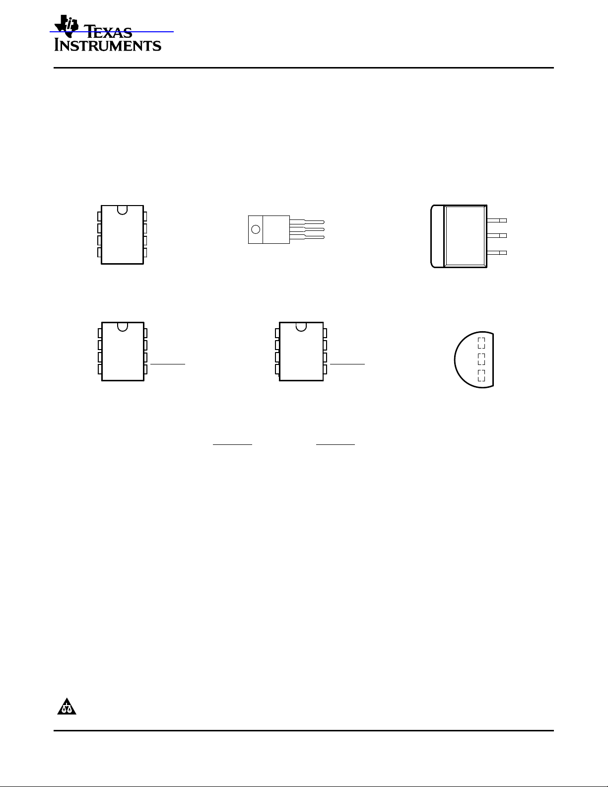
OUTPUT
COMMON
COMMON
NC
INPUT
COMMON
COMMON
NC
TL750L. . . D PACKAGE
(TOP VIEW)
TL750L. . . KC PACKAGE
(TOP VIEW)
TL750L. . . LP PACKAGE
(TO-92, TO-226AA)
(TOP VIEW)
OUTPUT
COMMON
COMMON
NC
INPUT
COMMON
COMMON
ENABLE
OUTPUT
NC
NC
NC
INPUT
NC
COMMON
ENABLE
TL751L. . . D PACKAGE
(TOP VIEW)
TL751L. . . P PACKAGE
(TOP VIEW)
1
2
3
4
8
7
6
5
1
2
3
4
8
7
6
5
1
2
3
4
INPUT
COMMON
OUTPUT
NC − No internal connection
TL750L. . . KTE PACKAGE
(TOP VIEW)
OUTPUT
COMMON
INPUT
COMMON
COMMON
OUTPUT
INPUT
COMMON
NC − No internal connection
NC − No internal connection
查询TL750L08CD供应商
TL750L, TL751L SERIES
LOW-DROPOUT VOLTAGE REGULATORS
SLVS017S – SEPTEMBER 1987 – REVISED AUGUST 2005
FEATURES
• Very Low Dropout Voltage, Less Than 0.6 V at • Reverse Transient Protection Down to –50 V
150 mA
• Very Low Quiescent Current
• TTL- and CMOS-Compatible Enable on
TL751L Series
• 60-V Load-Dump Protection
• Internal Thermal-Overload Protection
• Overvoltage Protection
• Internal Overcurrent-Limiting Circuitry
• Less Than 500- µ A Disable (TL751L Series)
DESCRIPTION/ORDERING INFORMATION
The TL750L and TL751L series of fixed-output voltage regulators offer 5-V, 8-V, 10-V, and 12-V options. The
TL751L series also has an enable ( ENABLE) input. When ENABLE is high, the regulator output is placed in the
high-impedance state. This gives the designer complete control over power up, power down, or emergency
shutdown.
The TL750L and TL751L series are low-dropout positive-voltage regulators specifically designed for
battery-powered systems. These devices incorporate overvoltage and current-limiting protection circuitry, along
with internal reverse-battery protection circuitry to protect the devices and the regulated system. The series is
fully protected against 60-V load-dump and reverse-battery conditions. Extremely low quiescent current during
full-load conditions makes these devices ideal for standby power systems.
PowerFLEX is a trademark of Texas Instruments.
PRODUCTION DATA information is current as of publication date.
Products conform to specifications per the terms of the Texas
Instruments standard warranty. Production processing does not
necessarily include testing of all parameters.
Please be aware that an important notice concerning availability, standard warranty, and use in critical applications of Texas
Instruments semiconductor products and disclaimers thereto appears at the end of this data sheet.
Copyright © 1987–2005, Texas Instruments Incorporated
www.ti.com
TL750L, TL751L SERIES
LOW-DROPOUT VOLTAGE REGULATORS
SLVS017S – SEPTEMBER 1987 – REVISED AUGUST 2005
ORDERING INFORMATION
T
J
0 ° C to 125 ° C PDIP – P Tube of 50 TL751L10CP TL751L10C
(1) Package drawings, standard packing quantities, thermal data, symbolization, and PCB design guidelines are available at
www.ti.com/sc/package.
(2) For the most current ordering information, see the Package Option Addendum at the end of this data sheet.
VOTYP
AT 25 ° C
PowerFLEX™ – KTE Reel of 2000 TL750L05CKTER TL750L05C
SOIC – D
5 V 51L05C
TO-226/TO-92 – LP 750L05C
TO-220 – KC Tube of 50 TL750L05CKC TL750L05C
8 V Reel of 2500 TL750L08CDR
10 V Tube of 75 TL751L10CD
12 V Tube of 75 TL751L12CD
SOIC – D 50L08C
TO-226/TO-92 – LP Bulk of 1000 TL750L08CLP 750L08C
SOIC – D
TO-226/TO-92 – LP 750L10C
SOIC – D
TO-226/TO-92 – LP Bulk of 1000 TL750L12CLP 750L12C
PACKAGE
(1)
Tube of 75 TL750L05CD
Reel of 2500 TL750L05CDR
Tube of 75 TL751L05CD
Reel of 2500 TL751L05CDR
Bulk of 1000 TL750L05CLP
Reel of 2000 TL750L05CLPR
Tube of 75 TL750L08CD
Tube of 75 TL750L10CD
Reel of 2500 TL750L10CDR
Reel of 2500 TL751L10CDR
Bulk of 1000 TL750L10CLP
Reel of 2000 TL750L10CLPR
Tube of 75 TL750L12CD
Reel of 2500 TL750L12CDR
Reel of 2500 TL751L12CDR
DEVICE COMPONENT COUNT
Transistors 20
JFETs 2
Diodes 5
Resistors 16
ORDERABLE PART NUMBER
(2)
TOP-SIDE MARKING
50L05C
50L10C
51L10C
50L12C
51L12C
2
www.ti.com
TL750L, TL751L SERIES
LOW-DROPOUT VOLTAGE REGULATORS
SLVS017S – SEPTEMBER 1987 – REVISED AUGUST 2005
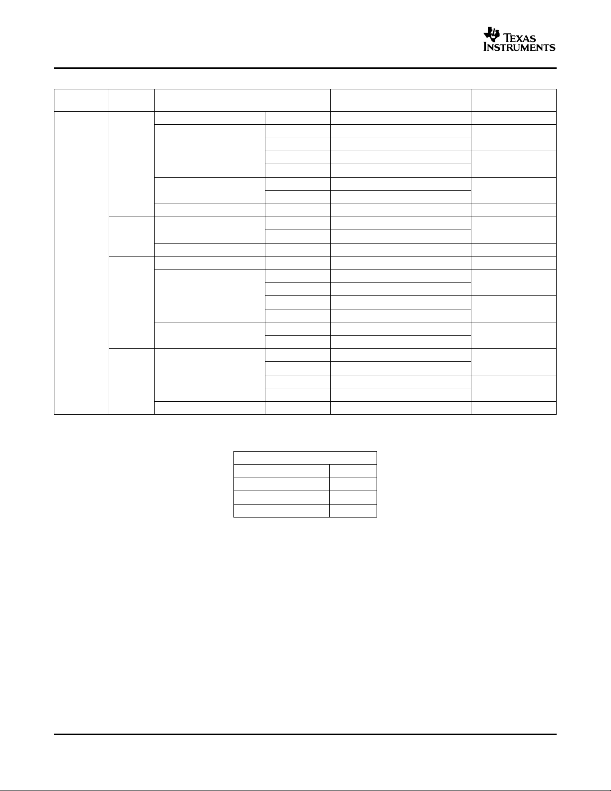
Absolute Maximum Ratings
over operating junction temperature range (unless otherwise noted)
Continuous input voltage 26 V
Transient input voltage
Continuous reverse input voltage –15 V
Transient reverse input voltage t ≤ 100 ms –50 V
T
J
T
stg
(1) Stresses beyond those listed under "absolute maximum ratings" may cause permanent damage to the device. These are stress ratings
(2) The transient input voltage rating applies to the waveform shown in Figure 1.
Operating virtual junction temperature 150 ° C
Lead temperature 1,6 mm (1/16 in) for 10 s 260 ° C
Storage temperature range –65 150 ° C
only, and functional operation of the device at these or any other conditions beyond those indicated under "recommended operating
conditions" is not implied. Exposure to absolute-maximum-rated conditions for extended periods may affect device reliability.
(1)
MIN MAX UNIT
(2)
TA= 25 ° C 60 V
Package Thermal Data
PACKAGE BOARD θ
(1)
JC
θ
JA
PDIP (P) High K, JESD 51-7 57 ° C/W 85 ° C/W
PowerFLEX™ (KTE) High K, JESD 51-5 3 ° C/W 23 ° C/W
SOIC (D) High K, JESD 51-7 39 ° C/W 97 ° C/W
TO-226/TO-92 (LP) High K, JESD 51-7 55 ° C/W 140 ° C/W
TO-220 (KC) High K, JESD 51-5 3 ° C/W 19 ° C/W
(1) Maximum power dissipation is a function of TJ(max), θJA, and TA. The maximum allowable power dissipation at any allowable ambient
temperature is PD= (TJ(max) – TA)/ θJA. Operating at the absolute maximum TJof 150 ° C can affect reliability.
Recommended Operating Conditions
over recommended operating junction temperature range (unless otherwise noted)
MIN MAX UNIT
TL75xL05 6 26
V
I
V
IH
V
IL
I
O
T
J
Input voltage V
High-level ENABLE input voltage TL75xLxx 2 15 V
(1)
Low-level ENABLE input voltage V
TJ= 25 ° C TL75xLxx –0.3 0.8
TJ= 0 ° C to 125 ° C TL75xLxx –0.15 0.8
Output current TL75xLxx 0 150 mA
Operating virtual junction temperature TL75xLxxC 0 125 ° C
(1) The algebraic convention, in which the least positive (most negative) value is designated minimum, is used in this data sheet for
ENABLE voltage levels and temperature only.
TL75xL08 9 26
TL75xL10 11 26
TL75xL12 13 26
3
www.ti.com
TL750L, TL751L SERIES
LOW-DROPOUT VOLTAGE REGULATORS
SLVS017S – SEPTEMBER 1987 – REVISED AUGUST 2005
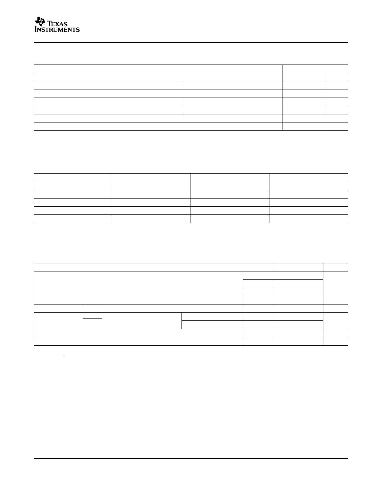
TL75xL05 Electrical Characteristics
VI= 14 V, IO= 10 mA, TJ= 25 ° C (unless otherwise noted)
PARAMETER TEST CONDITIONS UNIT
Output voltage VI= 6 V to 26 V, IO= 0 to 150 mA V
Input regulation voltage mV
Ripple rejection VI= 8 V to 18 V, f = 120 Hz 60 65 dB
Output regulation voltage IO= 5 mA to 150 mA 20 50 mV
Dropout voltage V
Output noise voltage f = 10 Hz to 100 kHz 500 µ V
Input bias current VI= 6 V to 26 V, IO= 10 mA, TJ= 0 ° C to 125 ° C 1 2 mA
(1) Pulse-testing techniques are used to maintain the junction temperature as close to the ambient temperature as possible. Thermal effects
must be taken into account separately. All characteristics are measured with a 0.1- µ F capacitor across the input and a 10- µ F capacitor,
with equivalent series resistance of less than 0.4 Ω , across the output.
VI= 9 V to 16 V 5 10
VI= 6 V to 26 V 6 30
IO= 10 mA 0.2
IO= 150 mA 0.6
IO= 150 mA 10 12
ENABLE ≥ 2 V 0.5
(1)
TL750L05
TL751L05
MIN TYP MAX
TJ= 25 ° C 4.8 5 5.2
TJ= 0 ° C to 125 ° C 4.75 5.25
TL75xL08 Electrical Characteristics
(1)
VI= 14 V, IO= 10 mA, TJ= 25 ° C (unless otherwise noted)
TL750L08
PARAMETER TEST CONDITIONS UNIT
Output voltage VI= 9 V to 26 V, IO= 0 to 150 mA V
Input regulation voltage mV
Ripple rejection VI= 11 V to 21 V, f = 120 Hz 60 65 dB
Output regulation voltage IO= 5 mA to 150 mA 40 80 mV
Dropout voltage V
Output noise voltage f = 10 Hz to 100 kHz 500 µ V
Input bias current VI= 9 V to 26 V, IO= 10 mA, TJ= 0 ° C to 125 ° C 1 2 mA
(1) Pulse-testing techniques are used to maintain the junction temperature as close to the ambient temperature as possible. Thermal effects
must be taken into account separately. All characteristics are measured with a 0.1- µ F capacitor across the input and a 10- µ F capacitor,
with equivalent series resistance of less than 0.4 Ω , across the output.
VI= 10 V to 17 V 10 20
VI= 9 V to 26 V 25 50
IO= 10 mA 0.2
IO= 150 mA 0.6
IO= 150 mA 10 12
ENABLE ≥ 2 V 0.5
TJ= 25 ° C 7.68 8 8.32
TJ= 0 ° C to 125 ° C 7.6 8.4
TL751L08
MIN TYP MAX
4
www.ti.com
TL750L, TL751L SERIES
LOW-DROPOUT VOLTAGE REGULATORS
SLVS017S – SEPTEMBER 1987 – REVISED AUGUST 2005
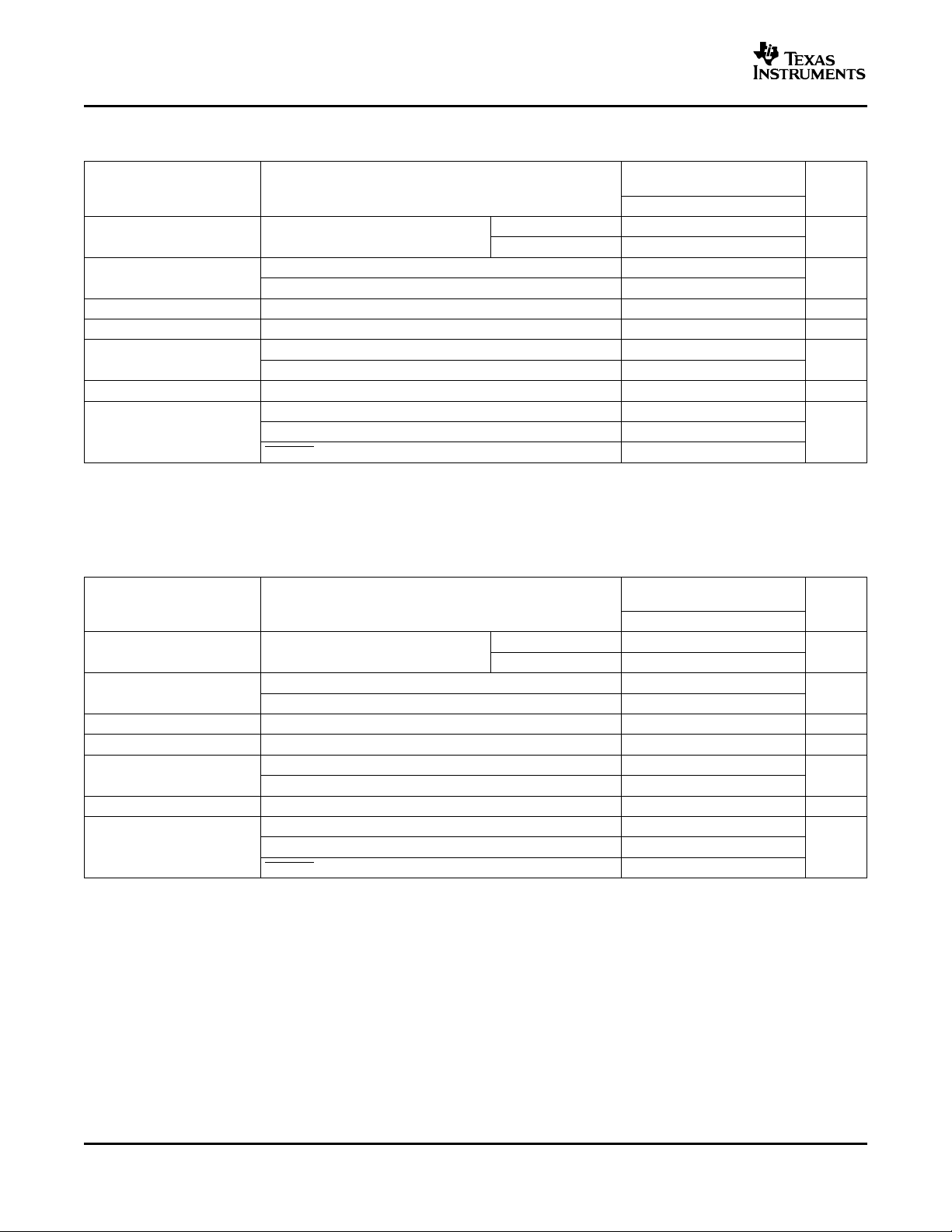
TL75xL10 Electrical Characteristics
VI= 14 V, IO= 10 mA, TJ= 25 ° C (unless otherwise noted)
PARAMETER TEST CONDITIONS UNIT
Output voltage VI= 11 V to 26 V, IO= 0 to 150 mA V
Input regulation voltage mV
Ripple rejection VI= 12 V to 22 V, f = 120 Hz 60 65 dB
Output regulation voltage IO= 5 mA to 150 mA 50 100 mV
Dropout voltage V
Output noise voltage f = 10 Hz to 100 kHz 700 µ V
Input bias current VI= 11 V to 26 V, IO= 10 mA, TJ= 0 ° C to 125 ° C 1 2 mA
(1) Pulse-testing techniques are used to maintain the junction temperature as close to the ambient temperature as possible. Thermal effects
must be taken into account separately. All characteristics are measured with a 0.1- µ F capacitor across the input and a 10- µ F capacitor,
with equivalent series resistance of less than 0.4 Ω , across the output.
VI= 12 V to 19 V 10 25
VI= 11 V to 26 V 30 60
IO= 10 mA 0.2
IO= 150 mA 0.6
IO= 150 mA 10 12
ENABLE ≥ 2 V 0.5
(1)
TL750L10
TL751L10
MIN TYP MAX
TJ= 25 ° C 9.6 10 10.4
TJ= 0 ° C to 125 ° C 9.5 10.5
TL75xL12 Electrical Characteristics
(1)
VI= 14 V, IO= 10 mA, TJ= 25 ° C (unless otherwise noted)
TL750L12
PARAMETER TEST CONDITIONS UNIT
Output voltage VI= 13 V to 26 V, IO= 0 to 150 mA V
Input regulation voltage mV
Ripple rejection VI= 13 V to 23 V, f = 120 Hz 50 55 dB
Output regulation voltage IO= 5 mA to 150 mA 50 120 mV
Dropout voltage V
Output noise voltage f = 10 Hz to 100 kHz 700 µ V
Input bias current VI= 13 V to 26 V, IO= 10 mA, TJ= 0 ° C to 125 ° C 1 2 mA
(1) Pulse-testing techniques are used to maintain the junction temperature as close to the ambient temperature as possible. Thermal effects
must be taken into account separately. All characteristics are measured with a 0.1- µ F capacitor across the input and a 10- µ F capacitor,
with equivalent series resistance of less than 0.4 Ω , across the output.
VI= 14 V to 19 V 15 30
VI= 13 V to 26 V 20 40
IO= 10 mA 0.2
IO= 150 mA 0.6
IO= 150 mA 10 12
ENABLE ≥ 2 V 0.5
TJ= 25 ° C 11.52 12 12.48
TJ= 0 ° C to 125 ° C 11.4 12.6
TL751L12
MIN TYP MAX
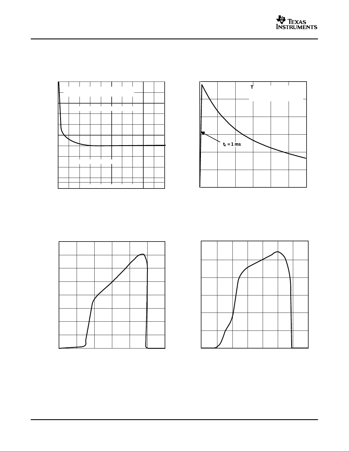
PARAMETER MEASUREMENT INFORMATION
The TL750L, TL751L series are low-dropout regulators. This means that capacitance loading is important to the
performance of the regulator because it is a vital part of the control loop. The capacitor value and its equivalent
series resistance (ESR) both affect the control loop and must be defined for the load range and temperature
range. Figure 1 shows the recommended range of ESR for a given load with a 10- µ F capacitor on the output.
5
www.ti.com
30
20
0 100 200
40
60
300 400 500
600
i
V − Transient Input Voltage − V
0
10
50
tr = 1 ms
TA = 25°C
VI = 14 V + 46e
(−t/0.230)
for t ≥ 5 ms
t − Time − ms
IL − Load Current − mA
0.2
0.1
0
0 10
ESR − Equivalent Series Resistance −
0.3
0.4
0.5
0.024
0.6
0.7
0.8
0.9
1.0
Region of Best Stability
80 120 150
Potential Instability Region
CL = 10-µF Tantalum Capacitor
TA = −40°C to 125°C
Potential Instability Region
Ω
30
20
10
0
0 2 4
40
50
60
6 8 12 1410
VI − Input Voltage − V
− Input Current − mAI
I
20
15
5
0
0 1 2 3
− Input Current − mA
25
35
40
4 5 6
30
10
I
I
VI − Input Voltage − V
TL750L, TL751L SERIES
LOW-DROPOUT VOLTAGE REGULATORS
SLVS017S – SEPTEMBER 1987 – REVISED AUGUST 2005
TYPICAL CHARACTERISTICS
EQUIVALENT SERIES RESISTANCE vs
TL750L05 TRANSIENT INPUT VOLTAGE
vs TIME
LOAD CURRENT
Figure 1. Figure 2.
TL750L05 TL750L12
INPUT CURRENT INPUT CURRENT
vs vs
INPUT VOLTAGE INPUT VOLTAGE
6
Figure 3. Figure 4.

PACKAGE OPTION ADDENDUM
www.ti.com
PACKAGING INFORMATION
Orderable Device Status
5962-9166901Q2A OBSOLETE LCCC FK 20 TBD Call TI Call TI
5962-9166901QPA OBSOLETE CDIP JG 8 TBD Call TI Call TI
TL750L05CD ACTIVE SOIC D 8 75 Green (RoHS &
TL750L05CDE4 ACTIVE SOIC D 8 75 Green (RoHS &
TL750L05CDR ACTIVE SOIC D 8 2500 Green (RoHS &
TL750L05CDRE4 ACTIVE SOIC D 8 2500 Green (RoHS &
TL750L05CKC ACTIVE TO-220 KC 3 50 TBD CU SNPB Level-NC-NC-NC
TL750L05CKTER ACTIVE PFM KTE 3 2000 TBD CU SNPB Level-1-220C-UNLIM
TL750L05CLP ACTIVE TO-92 LP 3 1000 TBD CU SNPB Level-NC-NC-NC
TL750L05CLPM OBSOLETE TO-92 LP 3 TBD Call TI Call TI
TL750L05CLPR ACTIVE TO-92 LP 3 2000 TBD CU SNPB Level-NC-NC-NC
TL750L05CP OBSOLETE PDIP P 8 TBD Call TI Call TI
TL750L05QD OBSOLETE SOIC D 8 TBD Call TI Call TI
TL750L05QDR OBSOLETE SOIC D 8 TBD Call TI Call TI
TL750L05QKC OBSOLETE TO-220 KC 3 TBD Call TI Call TI
TL750L05QLP OBSOLETE TO-92 LP 3 TBD Call TI Call TI
TL750L05QP OBSOLETE PDIP P 8 TBD Call TI Call TI
TL750L08CD ACTIVE SOIC D 8 75 Green (RoHS &
TL750L08CDE4 ACTIVE SOIC D 8 75 Green (RoHS &
TL750L08CDR ACTIVE SOIC D 8 2500 Green (RoHS &
TL750L08CDRE4 ACTIVE SOIC D 8 2500 Green (RoHS &
TL750L08CKC OBSOLETE TO-220 KC 3 TBD Call TI Call TI
TL750L08CLP ACTIVE TO-92 LP 3 1000 TBD CU SNPB Level-NC-NC-NC
TL750L08CP OBSOLETE PDIP P 8 TBD Call TI Call TI
TL750L08QD OBSOLETE SOIC D 8 TBD Call TI Call TI
TL750L08QDR OBSOLETE SOIC D 8 TBD Call TI Call TI
TL750L08QKC OBSOLETE TO-220 KC 3 TBD Call TI Call TI
TL750L08QLP OBSOLETE TO-92 LP 3 TBD Call TI Call TI
TL750L10CD ACTIVE SOIC D 8 75 Green (RoHS &
TL750L10CDE4 ACTIVE SOIC D 8 75 Green (RoHS &
TL750L10CDR ACTIVE SOIC D 8 2500 Green (RoHS &
TL750L10CDRE4 ACTIVE SOIC D 8 2500 Green (RoHS &
TL750L10CKC OBSOLETE TO-220 KC 3 TBD Call TI Call TI
TL750L10CLP ACTIVE TO-92 LP 3 1000 TBD CU SNPB Level-NC-NC-NC
(1)
Package
Type
Package
Drawing
Pins Package
Qty
Eco Plan
no Sb/Br)
no Sb/Br)
no Sb/Br)
no Sb/Br)
no Sb/Br)
no Sb/Br)
no Sb/Br)
no Sb/Br)
no Sb/Br)
no Sb/Br)
no Sb/Br)
no Sb/Br)
(2)
Lead/Ball Finish MSL Peak Temp
CU NIPDAU Level-2-260C-1YEAR
CU NIPDAU Level-2-260C-1YEAR
CU NIPDAU Level-2-260C-1YEAR
CU NIPDAU Level-2-260C-1YEAR
CU NIPDAU Level-2-260C-1YEAR
CU NIPDAU Level-2-260C-1YEAR
CU NIPDAU Level-2-260C-1YEAR
CU NIPDAU Level-2-260C-1YEAR
CU NIPDAU Level-2-260C-1YEAR
CU NIPDAU Level-2-260C-1YEAR
CU NIPDAU Level-2-260C-1YEAR
CU NIPDAU Level-2-260C-1YEAR
1-Aug-2005
(3)
Addendum-Page 1

PACKAGE OPTION ADDENDUM
www.ti.com
Orderable Device Status
(1)
Package
Type
Package
Drawing
Pins Package
Qty
Eco Plan
(2)
Lead/Ball Finish MSL Peak Temp
1-Aug-2005
TL750L10CLPR ACTIVE TO-92 LP 3 2000 TBD CU SNPB Level-NC-NC-NC
TL750L10CP OBSOLETE PDIP P 8 TBD Call TI Call TI
TL750L10QD OBSOLETE SOIC D 8 TBD Call TI Call TI
TL750L10QDR OBSOLETE SOIC D 8 TBD Call TI Call TI
TL750L10QKC OBSOLETE TO-220 KC 3 TBD Call TI Call TI
TL750L10QLP OBSOLETE TO-92 LP 3 TBD Call TI Call TI
TL750L10QP OBSOLETE PDIP P 8 TBD Call TI Call TI
TL750L12CD ACTIVE SOIC D 8 75 Green (RoHS &
CU NIPDAU Level-2-260C-1YEAR
no Sb/Br)
TL750L12CDE4 ACTIVE SOIC D 8 75 Green (RoHS &
CU NIPDAU Level-2-260C-1YEAR
no Sb/Br)
TL750L12CDR ACTIVE SOIC D 8 2500 Green (RoHS &
CU NIPDAU Level-2-260C-1YEAR
no Sb/Br)
TL750L12CDRE4 ACTIVE SOIC D 8 2500 Green (RoHS &
CU NIPDAU Level-2-260C-1YEAR
no Sb/Br)
TL750L12CKC OBSOLETE TO-220 KC 3 TBD Call TI Call TI
TL750L12CLP ACTIVE TO-92 LP 3 1000 TBD CU SNPB Level-NC-NC-NC
TL750L12CP OBSOLETE PDIP P 8 TBD Call TI Call TI
TL750L12QD OBSOLETE SOIC D 8 TBD Call TI Call TI
TL750L12QDR OBSOLETE SOIC D 8 TBD Call TI Call TI
TL750L12QKC OBSOLETE TO-220 KC 3 TBD Call TI Call TI
TL750L12QLP OBSOLETE TO-92 LP 3 TBD Call TI Call TI
TL750L12QP OBSOLETE SOIC D 8 TBD Call TI Call TI
TL751L05CD ACTIVE SOIC D 8 75 Green (RoHS &
CU NIPDAU Level-1-260C-UNLIM
no Sb/Br)
TL751L05CDE4 ACTIVE SOIC D 8 75 Green (RoHS &
CU NIPDAU Level-1-260C-UNLIM
no Sb/Br)
TL751L05CDR ACTIVE SOIC D 8 2500 Green (RoHS &
CU NIPDAU Level-1-260C-UNLIM
no Sb/Br)
TL751L05CDRE4 ACTIVE SOIC D 8 2500 Green (RoHS &
CU NIPDAU Level-1-260C-UNLIM
no Sb/Br)
TL751L05CP OBSOLETE PDIP P 8 TBD Call TI Call TI
TL751L05MFKB OBSOLETE LCCC FK 20 TBD Call TI Call TI
TL751L05MJGB OBSOLETE CDIP JG 8 TBD Call TI Call TI
TL751L05QD OBSOLETE SOIC D 8 TBD Call TI Call TI
TL751L05QDR OBSOLETE SOIC D 8 TBD Call TI Call TI
TL751L05QP OBSOLETE PDIP P 8 TBD Call TI Call TI
TL751L08CD OBSOLETE SOIC D 8 TBD Call TI Call TI
TL751L08CP OBSOLETE PDIP P 8 TBD Call TI Call TI
TL751L08QD OBSOLETE SOIC D 8 TBD Call TI Call TI
TL751L08QDR OBSOLETE SOIC D 8 TBD Call TI Call TI
TL751L10CD ACTIVE SOIC D 8 75 Green (RoHS &
CU NIPDAU Level-2-260C-1YEAR
no Sb/Br)
TL751L10CDE4 ACTIVE SOIC D 8 75 Green (RoHS &
CU NIPDAU Level-2-260C-1YEAR
no Sb/Br)
TL751L10CDR ACTIVE SOIC D 8 2500 Green (RoHS &
CU NIPDAU Level-2-260C-1YEAR
no Sb/Br)
(3)
Addendum-Page 2

PACKAGE OPTION ADDENDUM
www.ti.com
Orderable Device Status
(1)
Package
Type
Package
Drawing
Pins Package
Qty
Eco Plan
(2)
TL751L10CDRE4 ACTIVE SOIC D 8 2500 Green (RoHS &
Lead/Ball Finish MSL Peak Temp
CU NIPDAU Level-2-260C-1YEAR
1-Aug-2005
(3)
no Sb/Br)
TL751L10CP ACTIVE PDIP P 8 50 Pb-Free
CU NIPDAU Level-NC-NC-NC
(RoHS)
TL751L10CPE4 ACTIVE PDIP P 8 50 Pb-Free
CU NIPDAU Level-NC-NC-NC
(RoHS)
TL751L10QD OBSOLETE SOIC D 8 TBD Call TI Call TI
TL751L10QP OBSOLETE PDIP P 8 TBD Call TI Call TI
TL751L12CD ACTIVE SOIC D 8 75 Green (RoHS &
CU NIPDAU Level-2-260C-1YEAR
no Sb/Br)
TL751L12CDE4 ACTIVE SOIC D 8 75 Green (RoHS &
CU NIPDAU Level-2-260C-1YEAR
no Sb/Br)
TL751L12CDR ACTIVE SOIC D 8 2500 Green (RoHS &
CU NIPDAU Level-2-260C-1YEAR
no Sb/Br)
TL751L12CDRE4 ACTIVE SOIC D 8 2500 Green (RoHS &
CU NIPDAU Level-2-260C-1YEAR
no Sb/Br)
TL751L12CP OBSOLETE PDIP P 8 TBD Call TI Call TI
TL751L12MFKB OBSOLETE LCCC FK 20 TBD Call TI Call TI
TL751L12MJGB OBSOLETE CDIP JG 8 TBD Call TI Call TI
TL751L12QD OBSOLETE SOIC D 8 TBD Call TI Call TI
TL751L12QDR OBSOLETE SOIC D 8 TBD Call TI Call TI
TL751L12QP OBSOLETE PDIP P 8 TBD Call TI Call TI
(1)
The marketing status values are defined as follows:
ACTIVE: Product device recommended for new designs.
LIFEBUY: TI has announced that the device will be discontinued, and a lifetime-buy period is in effect.
NRND: Not recommended for new designs. Device is in production to support existing customers, but TI does not recommend using this part in
a new design.
PREVIEW: Device has been announced but is not in production. Samples may or may not be available.
OBSOLETE: TI has discontinued the production of the device.
(2)
Eco Plan - The planned eco-friendly classification: Pb-Free (RoHS) or Green (RoHS & no Sb/Br) - please check
http://www.ti.com/productcontent for the latest availability information and additional product content details.
TBD: The Pb-Free/Green conversion plan has not been defined.
Pb-Free (RoHS): TI's terms "Lead-Free" or "Pb-Free" mean semiconductor products that are compatible with the current RoHS requirements
for all 6 substances, including the requirement that lead not exceed 0.1% by weight in homogeneous materials. Where designed to be soldered
at high temperatures, TI Pb-Free products are suitable for use in specified lead-free processes.
Green (RoHS & no Sb/Br): TI defines "Green" to mean Pb-Free (RoHS compatible), and free of Bromine (Br) and Antimony (Sb) based flame
retardants (Br or Sb do not exceed 0.1% by weight in homogeneous material)
(3)
MSL, Peak Temp. -- The Moisture Sensitivity Level rating according to the JEDEC industry standard classifications, and peak solder
temperature.
Important Information and Disclaimer:The information provided on this page represents TI's knowledge and belief as of the date that it is
provided. TI bases its knowledge and belief on information provided by third parties, and makes no representation or warranty as to the
accuracy of such information. Efforts are underway to better integrate information from third parties. TI has taken and continues to take
reasonable steps to provide representative and accurate information but may not have conducted destructive testing or chemical analysis on
incoming materials and chemicals. TI and TI suppliers consider certain information to be proprietary, and thus CAS numbers and other limited
information may not be available for release.
In no event shall TI's liability arising out of such information exceed the total purchase price of the TI part(s) at issue in this document sold by TI
to Customer on an annual basis.
Addendum-Page 3

MECHANICAL DAT A
MCER001A – JANUARY 1995 – REVISED JANUARY 1997
JG (R-GDIP-T8) CERAMIC DUAL-IN-LINE
0.400 (10,16)
0.355 (9,00)
0.063 (1,60)
0.015 (0,38)
0.100 (2,54)
8
1
5
4
0.065 (1,65)
0.045 (1,14)
0.020 (0,51) MIN
0.023 (0,58)
0.015 (0,38)
0.280 (7,11)
0.245 (6,22)
0.310 (7,87)
0.290 (7,37)
0.200 (5,08) MAX
Seating Plane
0.130 (3,30) MIN
0°–15°
0.014 (0,36)
0.008 (0,20)
NOTES: A. All linear dimensions are in inches (millimeters).
B. This drawing is subject to change without notice.
C. This package can be hermetically sealed with a ceramic lid using glass frit.
D. Index point is provided on cap for terminal identification.
E. Falls within MIL STD 1835 GDIP1-T8
4040107/C 08/96
POST OFFICE BOX 655303 • DALLAS, TEXAS 75265

MECHANICAL DATA
MLCC006B – OCTOBER 1996
FK (S-CQCC-N**) LEADLESS CERAMIC CHIP CARRIER
28 TERMINAL SHOWN
A SQ
B SQ
19
20
21
22
23
24
25
12826 27
12
1314151618 17
0.020 (0,51)
0.010 (0,25)
MIN
0.342
(8,69)
0.442
0.640
0.739
0.938
1.141
A
0.358
(9,09)
0.458
(11,63)
0.660
(16,76)
0.761
(19,32)(18,78)
0.962
(24,43)
1.165
(29,59)
NO. OF
TERMINALS
**
11
10
9
8
7
6
5
432
20
28
44
52
68
84
0.020 (0,51)
0.010 (0,25)
(11,23)
(16,26)
(23,83)
(28,99)
MINMAX
0.307
(7,80)
0.406
(10,31)
0.495
(12,58)
0.495
(12,58)
0.850
(21,6)
1.047
(26,6)
0.080 (2,03)
0.064 (1,63)
B
MAX
0.358
(9,09)
0.458
(11,63)
0.560
(14,22)
0.560
(14,22)
0.858
(21,8)
1.063
(27,0)
0.055 (1,40)
0.045 (1,14)
0.028 (0,71)
0.022 (0,54)
0.050 (1,27)
NOTES: A. All linear dimensions are in inches (millimeters).
B. This drawing is subject to change without notice.
C. This package can be hermetically sealed with a metal lid.
D. The terminals are gold plated.
E. Falls within JEDEC MS-004
POST OFFICE BOX 655303 • DALLAS, TEXAS 75265
0.045 (1,14)
0.035 (0,89)
0.045 (1,14)
0.035 (0,89)
4040140/D 10/96

MECHANICAL DAT A
MPDI001A – JANUARY 1995 – REVISED JUNE 1999
P (R-PDIP-T8) PLASTIC DUAL-IN-LINE
0.400 (10,60)
0.355 (9,02)
8
5
0.260 (6,60)
0.240 (6,10)
1
0.021 (0,53)
0.015 (0,38)
NOTES: A. All linear dimensions are in inches (millimeters).
B. This drawing is subject to change without notice.
C. Falls within JEDEC MS-001
4
0.070 (1,78) MAX
0.020 (0,51) MIN
0.200 (5,08) MAX
0.125 (3,18) MIN
0.100 (2,54)
0.010 (0,25)
Seating Plane
M
0.325 (8,26)
0.300 (7,62)
0.015 (0,38)
Gage Plane
0.010 (0,25) NOM
0.430 (10,92)
MAX
4040082/D 05/98
For the latest package information, go to http://www.ti.com/sc/docs/package/pkg_info.htm
POST OFFICE BOX 655303 • DALLAS, TEXAS 75265

MECHANICAL DATA
MPFM001E – OCTOBER 1994 – REVISED JANUARY 2001
KTE (R-PSFM-G3) PowerFLEX PLASTIC FLANGE-MOUNT
0.420 (10,67)
0.410 (10,41)
0.295 (7,49)
NOM
0.100 (2,54)
0.200 (5,08)
1
0.375 (9,52)
0.365 (9,27)
0.360 (9,14)
0.350 (8,89)
0.220 (5,59)
NOM
3
0.025 (0,63)
0.031 (0,79)
0.320 (8,13)
0.310 (7,87)
0.010 (0,25)
0.360 (9,14)
0.350 (8,89)
M
0.080 (2,03)
0.070 (1,78)
0.050 (1,27)
0.040 (1,02)
0.010 (0,25) NOM
Thermal Tab
(See Note C)
Seating Plane
0.004 (0,10)
0.005 (0,13)
0.001 (0,03)
NOTES: A. All linear dimensions are in inches (millimeters).
B. This drawing is subject to change without notice.
C. The center lead is in electrical contact with the thermal tab.
D. Dimensions do not include mold protrusions, not to exceed 0.006 (0,15).
E. Falls within JEDEC MO-169
PowerFLEX is a trademark of Texas Instruments.
0.010 (0,25)
NOM
0.041 (1,04)
0.031 (0,79)
Gage Plane
3°–6°
0.010 (0,25)
4073375/F 12/00
POST OFFICE BOX 655303 • DALLAS, TEXAS 75265
1


MECHANICAL DATA
MSOT002A – OCTOBER 1994 – REVISED NOVEMBER 2001
LP (O-PBCY-W3) PLASTIC CYLINDRICAL P ACKAGE
0.205 (5,21) 0.165 (4,19)
0.175 (4,44)
0.157 (4,00) MAX
DIA
0.210 (5,34)
0.170 (4,32)
0.500 (12,70) MIN
0.125 (3,17)
Seating
Plane
0.050 (1,27)
C
0.104 (2,65)
FORMED LEAD OPTION
0.135 (3,43) MIN
0.055 (1,40)
0.045 (1,14)
0.105 (2,67)
0.080 (2,03)
NOTES: A. All linear dimensions are in inches (millimeters).
B. This drawing is subject to change without notice.
C. Lead dimensions are not controlled within this area
D. FAlls within JEDEC T O -226 Variation AA (TO-226 replaces TO-92)
E. Shipping Method:
Straight lead option available in bulk pack only.
Formed lead option available in tape & reel or ammo pack.
STRAIGHT LEAD OPTION
1
D
23
0.022 (0,56)
0.016 (0,41)
0.105 (2,67)
0.095 (2,41)
0.105 (2,67)
0.080 (2,03)
0.016 (0,41)
0.014 (0,35)
4040001-2/C 10/01
POST OFFICE BOX 655303 • DALLAS, TEXAS 75265
1

MECHANICAL DATA
MSOT002A – OCTOBER 1994 – REVISED NOVEMBER 2001
LP (O-PBCY-W3) PLASTIC CYLINDRICAL P ACKAGE
0.539 (13,70)
0.460 (11,70)
1.260 (32,00)
0.905 (23,00)
0.650 (16,50)
0.610 (15,50)
0.433 (11,00)
0.335 (8,50)
0.098 (2,50)
TAPE & REEL
0.020 (0,50) MIN
0.384 (9,75)
0.335 (8,50)
0.748 (19,00)
0.217 (5,50)
0.114 (2,90)
0.094 (2,40)
0.114 (2,90)
0.094 (2,40) 0.146 (3,70)
0.266 (6,75)
0.234 (5,95)
0.512 (13,00)
0.488 (12,40)
0.169 (4,30)
0.748 (19,00)
0.689 (17,50)
DIA
4040001-3/C 10/01
NOTES: A. All linear dimensions are in inches (millimeters).
2
B. This drawing is subject to change without notice.
C. Tape and Reel information for the Format Lead Option package.
POST OFFICE BOX 655303 • DALLAS, TEXAS 75265


IMPORTANT NOTICE
Texas Instruments Incorporated and its subsidiaries (TI) reserve the right to make corrections, modifications,
enhancements, improvements, and other changes to its products and services at any time and to discontinue
any product or service without notice. Customers should obtain the latest relevant information before placing
orders and should verify that such information is current and complete. All products are sold subject to TI’s terms
and conditions of sale supplied at the time of order acknowledgment.
TI warrants performance of its hardware products to the specifications applicable at the time of sale in
accordance with TI’s standard warranty. Testing and other quality control techniques are used to the extent TI
deems necessary to support this warranty . Except where mandated by government requirements, testing of all
parameters of each product is not necessarily performed.
TI assumes no liability for applications assistance or customer product design. Customers are responsible for
their products and applications using TI components. To minimize the risks associated with customer products
and applications, customers should provide adequate design and operating safeguards.
TI does not warrant or represent that any license, either express or implied, is granted under any TI patent right,
copyright, mask work right, or other TI intellectual property right relating to any combination, machine, or process
in which TI products or services are used. Information published by TI regarding third-party products or services
does not constitute a license from TI to use such products or services or a warranty or endorsement thereof.
Use of such information may require a license from a third party under the patents or other intellectual property
of the third party, or a license from TI under the patents or other intellectual property of TI.
Reproduction of information in TI data books or data sheets is permissible only if reproduction is without
alteration and is accompanied by all associated warranties, conditions, limitations, and notices. Reproduction
of this information with alteration is an unfair and deceptive business practice. TI is not responsible or liable for
such altered documentation.
Resale of TI products or services with statements different from or beyond the parameters stated by TI for that
product or service voids all express and any implied warranties for the associated TI product or service and
is an unfair and deceptive business practice. TI is not responsible or liable for any such statements.
Following are URLs where you can obtain information on other Texas Instruments products and application
solutions:
Products Applications
Amplifiers amplifier.ti.com Audio www.ti.com/audio
Data Converters dataconverter.ti.com Automotive www.ti.com/automotive
DSP dsp.ti.com Broadband www.ti.com/broadband
Interface interface.ti.com Digital Control www.ti.com/digitalcontrol
Logic logic.ti.com Military www.ti.com/military
Power Mgmt power.ti.com Optical Networking www.ti.com/opticalnetwork
Microcontrollers microcontroller.ti.com Security www.ti.com/security
Telephony www.ti.com/telephony
Video & Imaging www.ti.com/video
Wireless www.ti.com/wireless
Mailing Address: Texas Instruments
Post Office Box 655303 Dallas, Texas 75265
Copyright 2005, Texas Instruments Incorporated

Copyright © Each Manufacturing Company.
All Datasheets cannot be modified without permission.
This datasheet has been download from :
www.AllDataSheet.com
100% Free DataSheet Search Site.
Free Download.
No Register.
Fast Search System.
www.AllDataSheet.com
 Loading...