

TL499A
WIDE-RANGE POWER-SUPPLY CONTROLLERS
SLVS029F – JANUARY 1984 – REVISED MAY 2000
D
Internal Series-Pass and Step-Up Switching
Regulator
D
Output Adjustable From 2.9 V to 30 V
D
1-V to 10-V Input for Switching Regulator
D
4.5-V to 32-V Input for Series Regulator
D
Externally Controlled Switching Current
D
No External Rectifier Required
SERIES IN1
SW REG IN2
SW CURRENT CTRL
P OR PS PACKAGE
(TOP VIEW)
1
REF
2
3
4
OUTPUT
8
GND (PWR)
7
SW IN
6
GND
5
description
The TL499A is an integrated circuit designed to provide a wide range of adjustable regulated supply voltages.
The regulated output voltage can be varied from 2.9 V to 30 V by adjusting two external resistors. When the
TL499A is ac-coupled to line power through a step-down transformer, it operates as a series dc voltage regulator
to maintain the regulated output voltage. With the addition of a battery from 1.1 V to 10 V, an inductor, a filter
capacitor, and two resistors, the TL499A operates as a step-up switching regulator during an ac-line failure.
The adjustable regulated output voltage makes the TL499A useful for a wide range of applications. Providing
backup power during an ac-line failure makes the TL499A extremely useful in microprocessor memory
applications.
The TL499AC is characterized for operation from –20°C to 85°C.
AVAILABLE OPTIONS
T
A
–20°C to 85°C TL499ACP TL499ACPS TL499AY
The PS package is available taped and reeled. Add the suffix R to device
type (e.g., TL499ACPSR). Chip forms are tested at 25°C.
PLASTIC DIP
(P)
PLASTIC
SMALL-OUTLINE
(PS)
CHIP FORM
(Y)
Please be aware that an important notice concerning availability, standard warranty, and use in critical applications of
Texas Instruments semiconductor products and disclaimers thereto appears at the end of this data sheet.
PRODUCTION DATA information is current as of publication date.
Products conform to specifications per the terms of Texas Instruments
standard warranty. Production processing does not necessarily include
testing of all parameters.
POST OFFICE BOX 655303 • DALLAS, TEXAS 75265
Copyright 2000, Texas Instruments Incorporated
1
TL499A
WIDE-RANGE POWER-SUPPLY CONTROLLERS
SLVS029F – JANUARY 1984 – REVISED MAY 2000
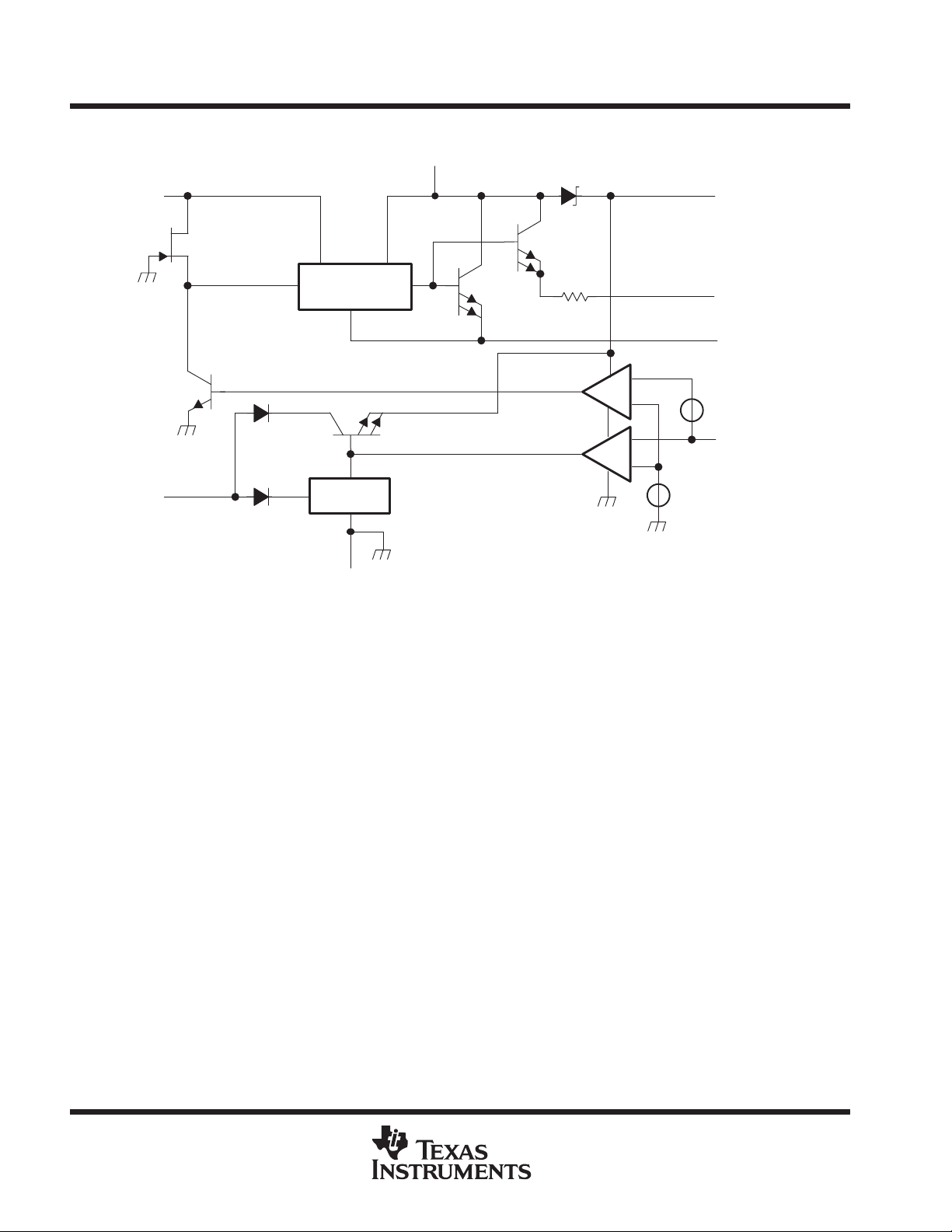
functional block diagram
SW IN
SW REG IN2
3
Startup
6
Voltage
Sense
Blocking Diode
8
OUTPUT
SERIES IN1
SW REG
Control
Current Sense
–
+
–
+
1
Startup
5
GND
7
GND (PWR)
4
SW CURRENT CTRL
+
2
REF
+
2
POST OFFICE BOX 655303 • DALLAS, TEXAS 75265
TL499A
WIDE-RANGE POWER-SUPPLY CONTROLLERS
SLVS029F – JANUARY 1984 – REVISED MAY 2000
absolute maximum ratings over operating free-air temperature range (unless otherwise noted)
†
Output voltage, VO (see Note 1) 35 V. . . . . . . . . . . . . . . . . . . . . . . . . . . . . . . . . . . . . . . . . . . . . . . . . . . . . . . . . . . . .
Input voltage, series regulator, VI1 35 V. . . . . . . . . . . . . . . . . . . . . . . . . . . . . . . . . . . . . . . . . . . . . . . . . . . . . . . . . . .
Input voltage, switching regulator, V
2 10 V. . . . . . . . . . . . . . . . . . . . . . . . . . . . . . . . . . . . . . . . . . . . . . . . . . . . . . . .
I
Blocking-diode reverse voltage 35 V. . . . . . . . . . . . . . . . . . . . . . . . . . . . . . . . . . . . . . . . . . . . . . . . . . . . . . . . . . . . . .
Blocking-diode forward current 1 A. . . . . . . . . . . . . . . . . . . . . . . . . . . . . . . . . . . . . . . . . . . . . . . . . . . . . . . . . . . . . . .
Power switch current (SW IN) 1 A. . . . . . . . . . . . . . . . . . . . . . . . . . . . . . . . . . . . . . . . . . . . . . . . . . . . . . . . . . . . . . . .
Package thermal impedance, θJA (see Notes 2 and 3): P package 85°C/W. . . . . . . . . . . . . . . . . . . . . . . . . . . .
PS package 95°C/W. . . . . . . . . . . . . . . . . . . . . . . . . . .
Lead temperature 1,6 mm (1/16 inch) from case for 10 seconds 260°C. . . . . . . . . . . . . . . . . . . . . . . . . . . . . . .
Storage temperature range, T
†
Stresses beyond those listed under “absolute maximum ratings” may cause permanent damage to the device. These are stress ratings only, and
functional operation of the device at these or any other conditions beyond those indicated under “recommended operating conditions” is not
implied. Exposure to absolute-maximum-rated conditions for extended periods may affect device reliability.
NOTES: 1. All voltage values are with respect to network ground terminal.
2. Maximum power dissipation is a function of TJ(max), θJA, and TA. The maximum allowable power dissipation at any allowable
ambient temperature is PD = (TJ(max) – TA)/θJA. Operating at the absolute maximum TJ of 150°C can affect reliability.
3. The package thermal impedance is calculated in accordance with JESD 51.
–65°C to 150°C. . . . . . . . . . . . . . . . . . . . . . . . . . . . . . . . . . . . . . . . . . . . . . . . . . .
stg
recommended operating conditions
MIN NOM MAX UNIT
Output voltage, V
Input voltage, VI1 (SERIES IN1) 4.5 32 V
Input voltage, VI2 (SW REG IN2) 1.1 10 V
Output-to-input differential voltage, switching regulator , VO – VI2 (see Note 4) 1.2 28.9 V
Continuous output current, I
Power switch current (at SW IN) 500 mA
Current-limiting resistor, R
Filter capacitor 100 470 µF
Pass capacitor 0.1 µF
Inductor, L (dcr ≤ 0.1 Ω) 50 150 µH
Operating free-air temperature, T
NOTE 4: When operating temperature range is TA ≤ 70°C, minimum VO – VI2 is ≥ 1.2 V. When operating temperature range is TA ≤85°C, minimum
VO – VI2 is ≥ 1.9 V.
O
O
CL
A
2.9 30 V
100 mA
150 1000 Ω
–20 85 °C
POST OFFICE BOX 655303 • DALLAS, TEXAS 75265
3

TL499A
PARAMETER
TEST CONDITIONS
UNIT
Switching regulator
mA
Standby current
PARAMETER
TEST CONDITIONS
UNIT
Switching regulator
mA
Standby current
WIDE-RANGE POWER-SUPPLY CONTROLLERS
SLVS029F – JANUARY 1984 – REVISED MAY 2000
electrical characteristics over recommended operating conditions (unless otherwise noted)
TL499AC
MIN TYP MAX
Voltage deviation (see Note 5) 20 30 mV/V
TA = –20°C to 70°C 1.2
Dropout voltage
Series regulator VI1 = 15 V, IO = 50 mA 1.8
Reference voltage (internal) VI2 = 5 V, VO = 3 V, IO = 1 mA 1.2 1.26 1.32 V
Reference-voltage change with temperature 5 10 mV/V
Output regulation (of reference voltage) IO = 1 mA to 50 mA 10 30 mV/V
VI2 = 1.1 V, VO = 12 V, RCL = 150 Ω, TA = 25°C 10
Output current
(see Figure 1)
NOTE 5: Voltage deviation is the output voltage difference that occurs in a change from series regulation to switching regulation:
Voltage deviation+V
Switching regulator
Series regulator 100
Switching regulator VI2 = 3 V, VO = 9 V, TA = 25°C 15 80 µA
Series regulator VI1 = 15 V, VO = 9 V, RE2 = 4.7 kΩ 0.8 1.2 mA
O
VI2 = 1.5 V, VO = 15 V, RCL = 150 Ω, TA = 25°C 15
VI2 = 6 V, VO = 30 V, RCL = 150 Ω, TA = 25°C 65
ǒ
series regulationǓ*
ǒ
V
switching regulation
O
Ǔ
1.9
V
electrical characteristics over recommended operating conditions, TA = 25°C (unless otherwise
noted)
TL499AY
MIN TYP MAX
Voltage deviation (see Note 5) 20 30 mV/V
TA = –20°C to 70°C 1.2
Dropout voltage
Series regulator VI1 = 15 V, IO = 50 mA 1.8
Reference voltage (internal) VI2 = 5 V, VO = 3 V, IO = 1 mA 1.2 1.26 1.32 V
Reference-voltage change with temperature TA = –20°C to 85°C 5 10 mV/V
Output regulation (of reference voltage) IO = 1 mA to 50 mA 10 30 mV/V
Output current
(see Figure 1)
NOTE 5: Voltage deviation is the output voltage difference that occurs in a change from series regulation to switching regulation:
Voltage deviation+V
Switching regulator
Series regulator 100
Switching regulator VI2 = 3 V, VO = 9 V 15 80 µA
Series regulator VI1 = 15 V, VO = 9 V, RE2 = 4.7 kΩ 0.8 1.2 mA
O
TA = –20°C to 85°C 1.9
VI2 = 1.1 V, VO = 12 V, RCL = 150 Ω 10
VI2 = 1.5 V, VO = 15 V, RCL = 150 Ω 15
VI2 = 6 V, VO = 30 V, RCL = 150 Ω 65
ǒ
series regulationǓ*
ǒ
V
switching regulation
O
Ǔ
V
4
POST OFFICE BOX 655303 • DALLAS, TEXAS 75265

OUTPUT
TL499A
WIDE-RANGE POWER-SUPPLY CONTROLLERS
SLVS029F – JANUARY 1984 – REVISED MAY 2000
APPLICATION INFORMATION
L = 50 µH
SERIES IN1
SW REG IN2
RCL = 500 Ω
1
3
1
SERIES IN1
2
REF
3
SW REG IN2
4
SW CURRENT
CTRL
TL499A
GND (PWR)
OUTPUT
SW IN
GND
8
7
6
5
CP = 0.01 µF
RE2 = 4.7 kΩ
+
RE1
Figure 1. TL499A Basic Configuration
Table 1. Maximum Output Current vs Input and Output Voltages
for Step-Up Switching Regulator With RCL = 150 Ω
SWITCHING REGULATOR INPUT VOLTAGE (SW REG IN2)
VOLTAGE
(V)
30 65 90
25 50 80 100
20 20 25 30 80 100 100
15 15 20 30 45 55 100 100 100
12 10 15 20 25 30 40 55 70 100 100 100
10 15 20 25 30 35 45 65 80 100 100
9 20 25 25 35 40 50 70 90 100 100
6 30 35 40 45 55 75 95 100
5 35 40 45 55 70 85 100 100 Circuit of Figure 1, except:
4.5 35 45 50 60 75 95 100 100
3 55 65
2.9 60
†
The difference between the output and input voltage for these combinations is greater than the minimum
output-to-input differential-voltage specification at 70°C (1.2 V), but less than the minimum at 85°C (1.9 V).
1.1 1.2 1.3 1.5 1.7 2 2.5 3 5 6 9
OUTPUT CURRENT
†
†
75
†
70
†
75†100†100
95†100
(V)
(mA)
†
†
†
RCL = 150 Ω
CF = 330 µF
CP = 0.1 µF
8
OUTPUT
CF = 470 µF
POST OFFICE BOX 655303 • DALLAS, TEXAS 75265
5

TL499A
OUTPUT
OUTPUT
WIDE-RANGE POWER-SUPPLY CONTROLLERS
SLVS029F – JANUARY 1984 – REVISED MAY 2000
APPLICATION INFORMATION
Table 2. Maximum Output Current vs Input and Output Voltages
for Step-Up Switching Regulator With RCL = 200 Ω
SWITCHING REGULATOR INPUT VOLTAGE (SW REG IN2)
VOLTAGE
(V)
30 50 100
25 50 70 100
20 15 25 30 70 90 100
15 10 15 25 35 45 90 100 100
12 10 10 15 20 25 35 45 60 100 100 100
10 15 20 20 25 30 40 55 70 100 100
9 20 20 25 30 35 45 60 80 100
6 25 30 35 45 50 65 90 100
5 30 35 40 55 60 75 100 100 Circuit of Figure 1, except:
4.5 35 40 45 55 65 85 100 100
3 50 55
2.9 50
†
The difference between the output and input voltage for these combinations is greater than the minimum
output-to-input differential-voltage specification at 70°C (1.2 V), but less than the minimum at 85°C (1.9 V).
1.1 1.2 1.3 1.5 1.7 2 2.5 3 5 6 9
OUTPUT CURRENT
†
†
†
†
80
90
85†100
65
†
†
60
65
(V)
(mA)
†
†
†
RCL = 200 Ω
CF = 330 µF
CP = 0.1 µF
Table 3. Maximum Output Current vs Input and Output Voltages
for Step-Up Switching Regulator With RCL = 300 Ω
SWITCHING REGULATOR INPUT VOLTAGE (SW REG IN2)
VOLTAGE
(V)
30 40 70
25 40 55 100
20 10 15 20 55 70 100
15 10 10 20 30 35 75 95 100
12 10 10 10 15 20 25 35 45 95 100 100
10 15 15 15 20 25 30 45 55 100 100
9 15 15 20 25 30 35 50 60 100 100
6 25 25 30 35 45 55 70 90
5 30 30 35 45 50 65 85 100 Circuit of Figure 1, except:
4.5 30 35 40 45 55 70 95 100
3 45 50
2.9 45
†
The difference between the output and input voltage for these combinations is greater than the minimum
output-to-input differential-voltage specification at 70°C (1.2 V), but less than the minimum at 85°C (1.9 V).
1.1 1.2 1.3 1.5 1.7 2 2.5 3 5 6 9
OUTPUT CURRENT
†
†
55
†
†
50
60
†
70
90
†
†
75
95
(V)
(mA)
†
†
†
RCL = 300 Ω
CF = 330 µF
CP = 0.1 µF
6
POST OFFICE BOX 655303 • DALLAS, TEXAS 75265
OUTPUT
OUTPUT
TL499A
WIDE-RANGE POWER-SUPPLY CONTROLLERS
SLVS029F – JANUARY 1984 – REVISED MAY 2000
APPLICATION INFORMATION
Table 4. Maximum Output Current vs Input and Output Voltages
for Step-Up Switching Regulator With RCL = 510 Ω
SWITCHING REGULATOR INPUT VOLTAGE (SW REG IN2)
VOLTAGE
(V)
30 30 50
25 25 40 75
20 40 55 90
15 15 20 55 70 100
12 10 15 25 35 65 80 100
10 10 20 25 30 40 70 85
9 10 10 10 15 20 25 35 45 75 100
6 15 20 20 25 30 35 50 60
5 20 20 25 30 35 45 55 70 Circuit of Figure 1, except:
4.5 20 25 30 35 40 50 65 90
3 35 35
2.9 35
†
The difference between the output and input voltage for these combinations is greater than the minimum
output-to-input differential-voltage specification at 70°C (1.2 V), but less than the minimum at 85°C (1.9 V).
1.1 1.2 1.3 1.5 1.7 2 2.5 3 5 6 9
OUTPUT CURRENT
†
†
40
†
35
†
†
40
50
55
†
75
†
80
(V)
(mA)
†
†
†
RCL = 510 Ω
CF = 330 µF
CP = 0.1 µF
Table 5. Maximum Output Current vs Input and Output Voltages
for Step-Up Switching Regulator With RCL = 1 kΩ
SWITCHING REGULATOR INPUT VOLTAGE (SW REG IN2)
VOLTAGE
(V)
30 35
25 35 50
20 35 60
15 10 30 45 65
12 20 40 45 85
10 15 25 40 55
9 10 10 15 25 30 45 60
6 10 10 10 15 20 20 30 35
5 10 10 15 20 20 25 35 40 Circuit of Figure 1, except:
4.5 15 15 15 20 25 30 40 45
3 20 25
2.9 20
†
The difference between the output and input voltage for these combinations is greater than the minimum
output-to-input differential-voltage specification at 70°C (1.2 V), but less than the minimum at 85°C (1.9 V).
1.1 1.2 1.3 1.5 1.7 2 2.5 3 5 6 9
OUTPUT CURRENT
†
†
25
†
25
†
†
25
30
30
†
35
†
45
(V)
(mA)
†
†
†
RCL = 1 kΩ
CF = 330 µF
CP = 0.1 µF
POST OFFICE BOX 655303 • DALLAS, TEXAS 75265
7

IMPORTANT NOTICE
T exas Instruments and its subsidiaries (TI) reserve the right to make changes to their products or to discontinue
any product or service without notice, and advise customers to obtain the latest version of relevant information
to verify, before placing orders, that information being relied on is current and complete. All products are sold
subject to the terms and conditions of sale supplied at the time of order acknowledgment, including those
pertaining to warranty, patent infringement, and limitation of liability.
TI warrants performance of its semiconductor products to the specifications applicable at the time of sale in
accordance with TI’s standard warranty. Testing and other quality control techniques are utilized to the extent
TI deems necessary to support this warranty . Specific testing of all parameters of each device is not necessarily
performed, except those mandated by government requirements.
Customers are responsible for their applications using TI components.
In order to minimize risks associated with the customer’s applications, adequate design and operating
safeguards must be provided by the customer to minimize inherent or procedural hazards.
TI assumes no liability for applications assistance or customer product design. TI does not warrant or represent
that any license, either express or implied, is granted under any patent right, copyright, mask work right, or other
intellectual property right of TI covering or relating to any combination, machine, or process in which such
semiconductor products or services might be or are used. TI’s publication of information regarding any third
party’s products or services does not constitute TI’s approval, warranty or endorsement thereof.
Copyright 2000, Texas Instruments Incorporated
 Loading...