D
Pin Compatible With ST16C2550 With
Additional Enhancements
D
Up to 1.5 Mbps Baud Rate When Using
Crystal (24 MHz Input Clock)
D
Up to 2.25 Mbps Baud Rate When Using
Oscillator or Clock Source (36 MHz Input
Clock)
D
64-Byte Transmit FIFO
D
64-Byte Receive FIFO With Error Flags
D
Programmable and Selectable Transmit and
Receive FIFO Trigger Levels for DMA and
Interrupt Generation
D
Programmable Receive FIFO Trigger Levels
for Software/Hardware Flow Control
D
Software/Hardware Flow Control
– Programmable Xon/Xoff Characters
– Programmable Auto-RTS and Auto-CTS
D
Optional Data Flow Resume by Xon Any
Character
D
DMA Signalling Capability for Both
Received and Transmitted Data
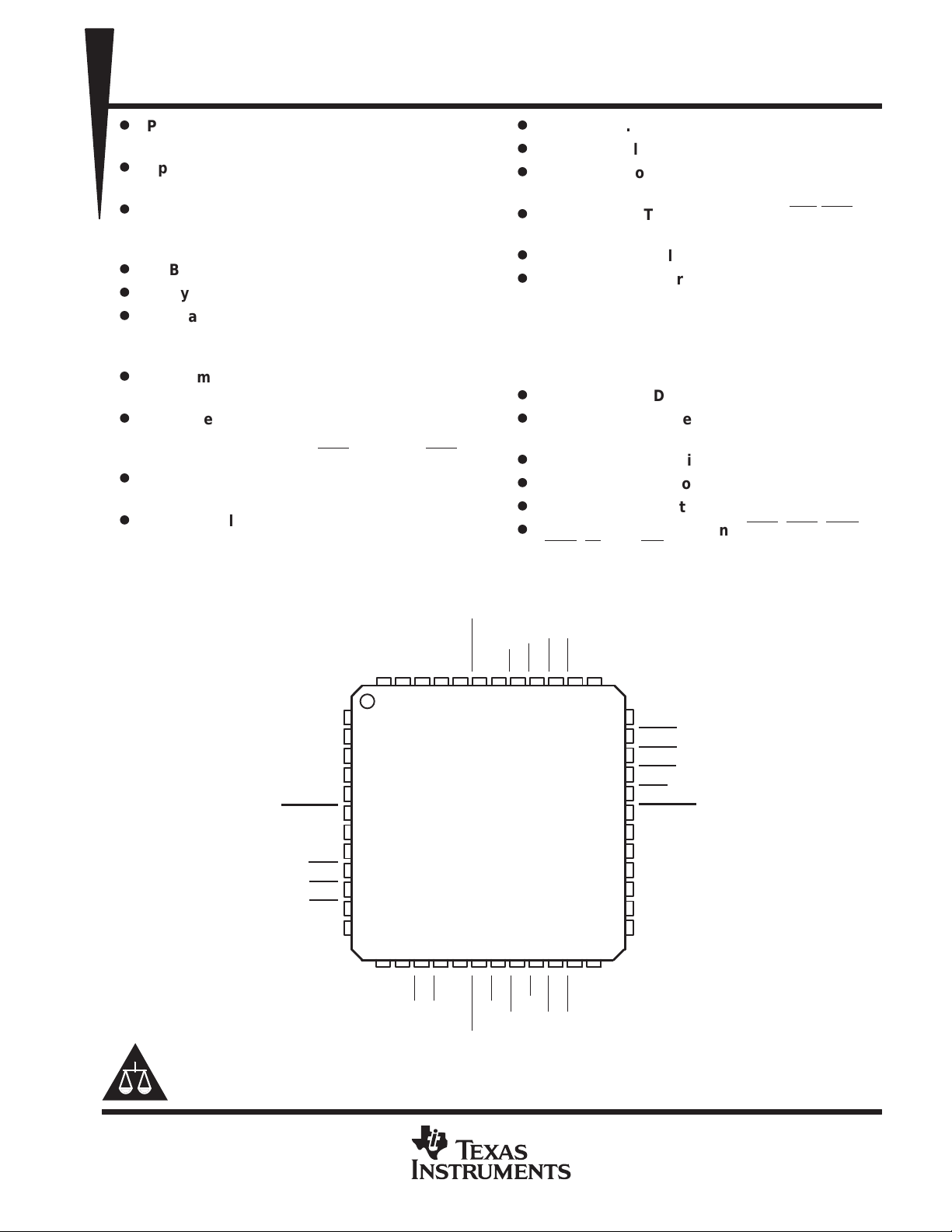
PACKAGE
(TOP VIEW)
TL16C752B
3.3-V DUAL UART WITH 64-BYTE FIFO
SLLS405 – DECEMBER 1999
D
Supports 3.3-V Operation
D
Software Selectable Baud Rate Generator
D
Prescaler Provides Additional Divide By 4
Function
D
Fast Access Time 2 Clock Cycle IOR/IOW
Pulse Width
D
Programmable Sleep Mode
D
Programmable Serial Interface
Characteristics
– 5, 6, 7, or 8 Bit Characters
– Even, Odd, or No Parity Bit Generation
and Detection
– 1, 1.5, or 2 Stop Bit Generation
D
False Start Bit Detection
D
Complete Status Reporting Capabilities in
Both Normal and Sleep Mode
D
Line Break Generation and Detection
D
Internal Test and Loopback Capabilities
D
Fully Prioritized Interrupt System Controls
D
Modem Control Functions (CTS, RTS, DSR,
DTR, RI, and CD)
CC
RIA
CDA
DSRA
RIB
RTSB
CTSA
NC
37
36
35
34
33
32
31
30
29
28
27
26
25
NC
CTSB
RESET
DTRB
DTRA
RTSA
OPA
RXRDYA
INTA
INTB
A0
A1
A2
NC
D4D3D2D1D0
47 46 45 44 4348 42
D5
1
D6
2
D7
3
RXB
4
RXA
5
TXRDYB
NC – No internal connection
Please be aware that an important notice concerning availability, standard warranty, and use in critical applications of
Texas Instruments semiconductor products and disclaimers thereto appears at the end of this data sheet.
TXA
TXB
OPB
CSA
CSB
NC
6
7
8
9
10
11
12
13
14 15
XTAL1
16
IOW
XTAL2
TXRDYA
17 18 19 20
CDB
GND
RXRDYB
V
40 39 3841
21 22 23 24
IOR
DSRB
PRODUCTION DATA information is current as of publication date.
Products conform to specifications per the terms of Texas Instruments
standard warranty. Production processing does not necessarily include
testing of all parameters.
POST OFFICE BOX 655303 • DALLAS, TEXAS 75265
Copyright 1999, Texas Instruments Incorporated
1
TL16C752B
I/O
DESCRIPTION
3.3-V DUAL UART WITH 64-BYTE FIFO
SLLS405 – DECEMBER 1999
description
The TL16C752B is a dual universal asynchronous receiver/transmitter (UART) with 64-byte FIFOs, automatic
hardware/software flow control, and data rates up to 3.125 Mbps. The TL16C752B offers enhanced features.
It has a transmission control register (TCR) that stores received FIFO threshold level to start/stop transmission
during hardware and sofware flow control. With the FIFO RDY register, the software gets the status of
TXRDY/RXRDY for all four ports in one access. On-chip status registers provide the user with error indications,
operational status and modem interface control. System interrupts may be tailored to meet user requirements.
An internal loopback capability allows onboard diagnostics.
The UART transmits data sent to it from the peripheral 8-bit bus on the TX signal and receives characters on
the RX signal. Characters can be programmed to be 5, 6, 7, or 8 bits. The UART has a 64-byte receive FIFO
and transmit FIFO and can be programmed to interrupt at different trigger levels. The UART generates its own
desired baud rate based upon a programmable divisor and its input clock. It can transmit even, odd, or no parity
and 1, 1.5, or 2 stop bits. The receiver can detect break, idle, or framing errors, FIFO overflow, and parity errors.
The transmitter can detect FIFO underflow. The UART also contains a software interface for modem control
operations, and has software flow control and hardware flow control capabilities.
The TL16C752B is available in a 48-pin PT (LQFP) package. The 48-pin version offers three state interrupt
control and provides constant active interrupt outputs.
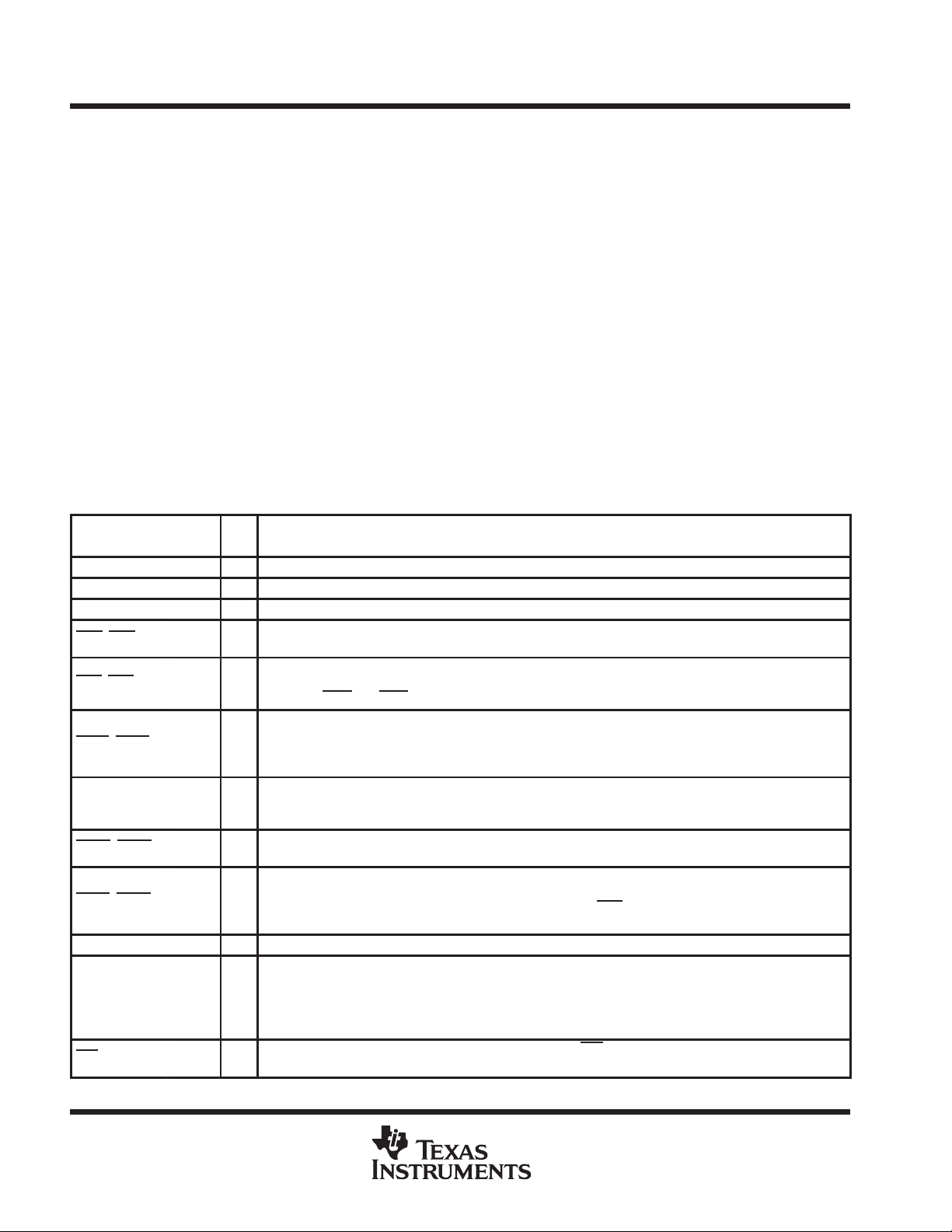
Terminal Functions
TERMINAL
NAME NO.
A0 28 I Address 0 select bit. Internal registers address selection
A1 27 I Address 1 select bit. Internal registers address selection
A2 26 I Address 2 select bit. Internal registers address selection
CDA, CDB 40, 16 I
CSA, CSB 10, 11 I
CTSA, CTSB 38, 23 I
D0–D4
D5–D7
DSRA, DSRB 39, 20 I
DTRA, DTRB 34, 35 O
GND 17 Pwr Signal and power ground
INTA, INTB 30, 29 O
IOR 19 I
44–48,
1–3
Carrier detect (active low). These inputs are associated with individual UART channels A and B. A low on
these pins indicates that a carrier has been detected by the modem for that channel.
Chip select A and B (active low). These pins enable data transfers between the user CPU and the TL16C752B
for the channel(s) addressed. Individual UART sections (A, B) are addressed by providing a low on the
respective CS A
Clear to send (active low). These inputs are associated with individual UART channels A and B. A logic low
on the CTS pins indicates the modem or data set is ready to accept transmit data from the 752B. Status can
be tested by reading MSR bit 4. These pins only affect the transmit and receive operations when auto CTS
function is enabled through the enhanced feature register (EFR) bit 7, for hardware flow control operation.
Data bus (bidirectional). These pins are the eight bit, 3-state data bus for transferring information to or from
the controlling CPU. D0 is the least significant bit and the first data bit in a transmit or receive serial data
I/O
stream.
Data set ready (active low). These inputs are associated with individual UART channels A and B. A logic low
on these pins indicates the modem or data set is powered on and is ready for data exchange with the UART .
Data terminal ready (active low). These outputs are associated with individual UART channels A and B. A
logic low on these pins indicates that the 752B is powered on and ready. These pins can be controlled through
the modem control register. Writing a 1 to MCR bit 0 sets the DTR
output of these pins is high after writing a 0 to MCR bit 0, or after a reset.
Interrupt A and B (active high). These pins provide individual channel interrupts, INT A and B. INT A and B
are enabled when MCR bit 3 is set to a logic 1, interrupts are enabled in the interrupt enable register (IER),
and when an interrupt condition exists. Interrupt conditions include: receiver errors, available receiver buffer
data, transmit buffer empty , or when a modem status flag is detected. INTA–B are in the high-impedance state
after reset.
Read input (active low strobe). A high to low transition on IOR will load the contents of an internal register
defined by address bits A0–A2 onto the TL16C752B data bus (D0–D7) for access by an external CPU.
and CS B pins.
output to low, enabling the modem. The
2
POST OFFICE BOX 655303 • DALLAS, TEXAS 75265
I/O
DESCRIPTION
TERMINAL
NAME NO.
IOW 15 I
OPA, OPB 32, 9 0
RESET 36 I
RIA, RIB 41, 21 I
RTSA, RTSB 33, 22 O
RXA, RXB 5, 4 I
RXRDYA,
RXRDYB
TXA, TXB 7, 8 O
TXRDYA,
TXRDYB
V
CC
XTAL1 13 I
XTAL2 14 O
31, 18 O
43, 6 O
42 I Power supply inputs.
TL16C752B
3.3-V DUAL UART WITH 64-BYTE FIFO
SLLS405 – DECEMBER 1999
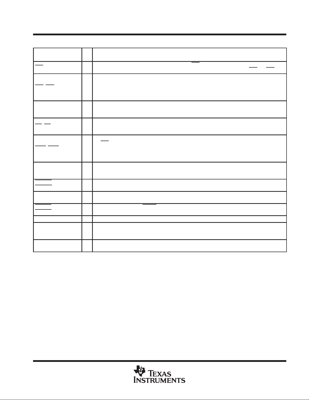
Terminal Functions (Continued)
Write input (active low strobe). A high to low transition on IOW will transfer the contents of the data bus (D0–D7)
from the external CPU to an internal register that is defined by address bits A0–A2 and CSA
User defined outputs. This function is associated with individual channels A and B. The state at these pins is
defined by the user and through the software settings of the MCR register, bit 3. INT A–B are set to active mode
and OP to a logic 0 when the MCR–3 is set to a logic 1. INTA–B are set to the 3-state mode and OP to a logic
1 when MCR-3 is set to a logic 0. See bit 3, Modem Control Register (MCR bit 3). The output of these two pins
is high after reset.
Reset. RESET will reset the internal registers and all the outputs. The UART transmitter output and the
receiver input will be disabled during reset time. See TL16C752B external reset conditions for initialization
details. RESET is an active -high input.
Ring indicator (active low). These inputs are associated with individual UART channels A and B. A logic low
on these pins indicates the modem has received a ringing signal from the telephone line. A low to high transition
on these input pins generates a modem status interrupt, if enabled.
Request to send (active low). These outputs are associated with individual UART channels A and B. A low on
the RTS
pins indicates the transmitter has data ready and waiting to send. Writing a 1 in the modem control
register (MCR bit 1) sets these pins to low, indicating data is available. After a reset, these pins are set to high.
These pins only affects the transmit and receive operation when auto RTS function is enabled through the
enhanced feature register (EFR) bit 6, for hardware flow control operation.
Receive data input. These inputs are associated with individual serial channel data to the 752B. During the
local loopback mode, these RX input pins are disabled and TX data is internally connected to the UART RX
input internally .
Receive ready (active low). RXRDY A and B goes low when the trigger level has been reached or a timeout
interrupt occurs. They go high when the RX FIFO is empty or there is an error in RX FIFO.
Transmit data. These outputs are associated with individual serial transmit channel data from the 752B. During
the local loopback mode, the TX input pin is disabled and TX data is internally connected to the UART RX input.
Transmit ready (active low). TXRDY A and B go low when there trigger level numbers of spares available. They
go high when the TX buffer is full.
Crystal or external clock input. XTAL1 functions as a crystal input or as an external clock input. A crystal can
be connected between XTAL1 and XTAL2 to form an internal oscillator circuit (see Figures 10 and 11).
Alternatively , an external clock can be connected to XTAL1 to provide custom data rates.
Output of the crystal oscillator or buffered clock. See also XT AL1. XT AL2 is used as a crystal oscillator output
or buffered a clock output.
and CSB
POST OFFICE BOX 655303 • DALLAS, TEXAS 75265
3
TL16C752B
3.3-V DUAL UART WITH 64-BYTE FIFO
SLLS405 – DECEMBER 1999
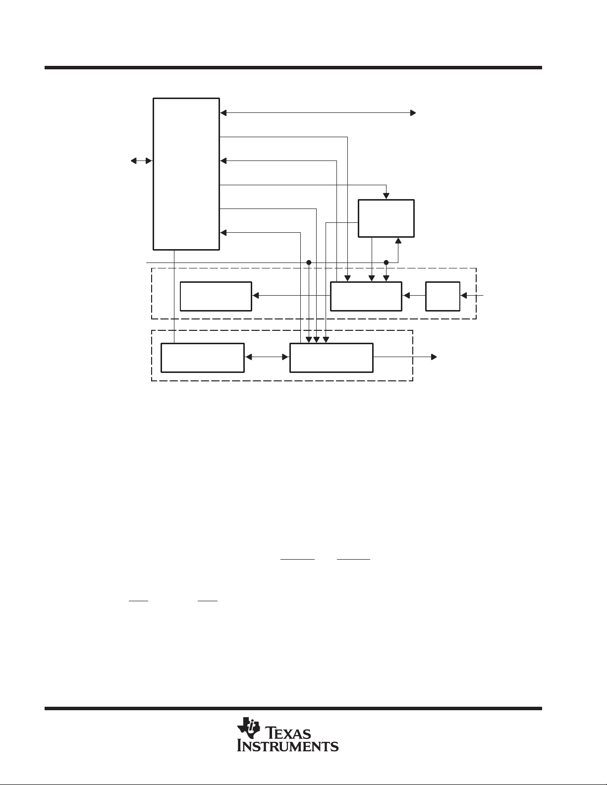
functional block diagram
Modem Control Signals
Control Signals
64-Byte
Status Signals
Divisor
Control Signals
Status Signals
Receiver Block
Logic
Transmitter Block
Logic
Baud-Rate
Generator
TX
Vote
Logic
TX
RX
RX
Bus
Interface
UART_CLK
NOTE: The vote logic determines whether the RX data is a logic 1 or 0. It takes three samples of the RX line, and uses a majority vote to determine
the logic level received. The vote logic operates on all bits received.
Control
and
Status Block
Receiver FIFO
Transmitter FIFO
64-Byte
functional description
The TL16C752B UART is pin compatible with the ST16C2550 UART. It provides more enhanced features. All
additional features are provided through a special enhanced feature register.
The UART will perform serial-to-parallel conversion on data characters received from peripheral devices or
modems and parallel-to-parallel conversion on data characters transmitted by the processor. The complete
status of each channel of the TL16C752B UART can be read at any time during functional operation by the
processor.
The TL16C752B can be placed in an alternate mode (FIFO mode) relieving the processor of excessive software
overhead by buffering received/transmitted characters. Both the receiver and transmitter FIFOs can store up
to 64 bytes (including three additional bits of error status per byte for the receiver FIFO) and have selectable
or programmable trigger levels. Primary outputs RXRDY
and TXRDY allow signalling of DMA transfers.
The TL16C752B has selectable hardware flow control and software flow control. Hardware flow control
significantly reduces software overhead and increases system efficiency by automatically controlling serial data
flow using the RTS output and CTS input signals. Software flow control automatically controls data flow by using
programmable Xon/Xoff characters.
The UART includes a programmable baud rate generator that can divide the timing reference clock input by a
divisor between 1 and (216–1).
4
POST OFFICE BOX 655303 • DALLAS, TEXAS 75265
TL16C752B
3.3-V DUAL UART WITH 64-BYTE FIFO
SLLS405 – DECEMBER 1999
functional description (continued)
trigger levels
The TL16C752B provides independent selectable and programmable trigger levels for both receiver and
transmitter DMA and interrupt generation. After reset, both transmitter and receiver FIFOs are disabled and so,
in effect, the trigger level is the default value of one byte. The selectable trigger levels are available via the FCR.
The programmable trigger levels are available via the TLR.
hardware flow control
Hardware flow control is composed on auto-CTS and auto-RTS. Auto-CTS and auto-RTS can be enabled/
disabled independently by programming EFR[7:6].
With auto-CTS, CTS must be active before the UART can transmit data.
Auto-RTS
the RTS
only activates the RTS output when there is enough room in the FIFO to receive data and deactivates
output when the RX FIFO is sufficiently full. The HALT and RESTORE trigger levels in the TCR
determine the levels at which RTS is activated/deactivated.
If both auto-CTS
and auto-RTS are enabled, when RTS is connected to CTS, data transmission does not occur
unless the receiver FIFO has empty space. Thus, overrun errors are eliminated during hardware flow control.
If not enabled, overrun errors occur if the transmit data rate exceeds the receive FIFO servicing latency.
auto-RTS
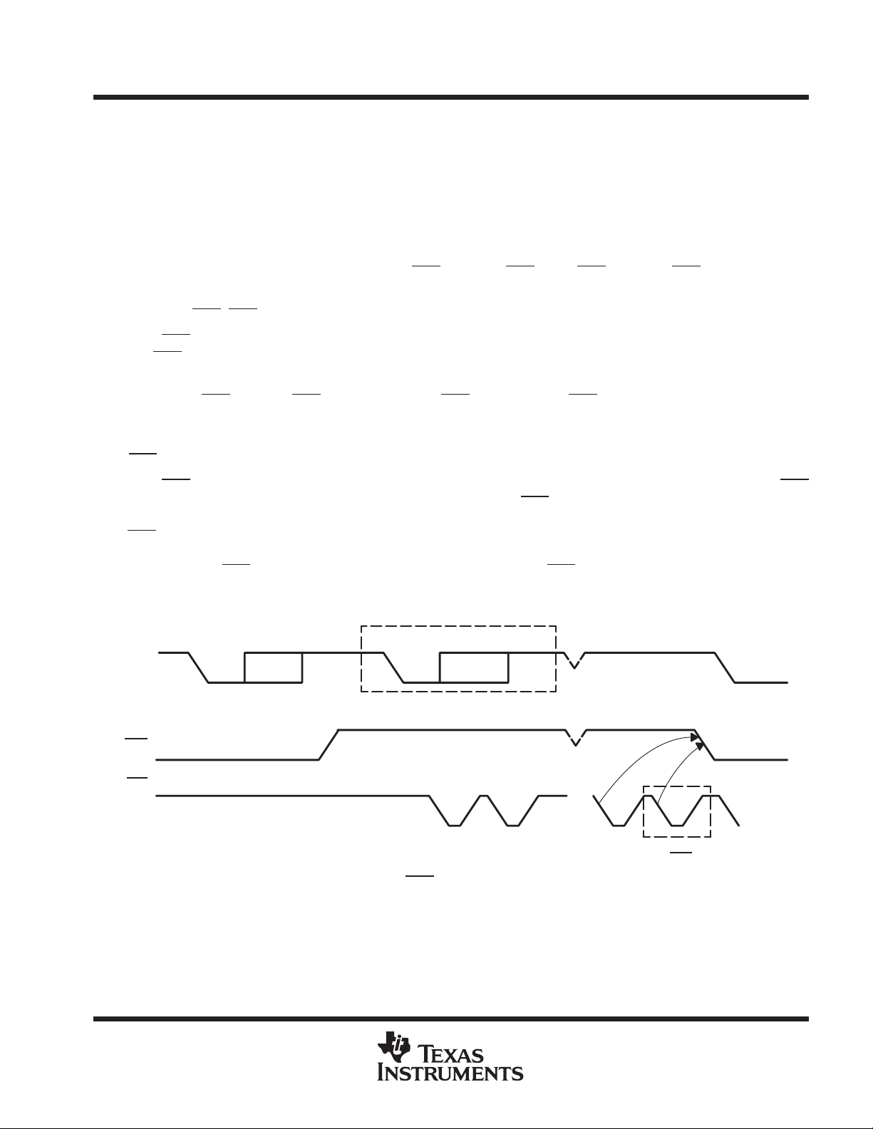
Auto-RTS data flow control originates in the receiver block (see functional block diagram). Figure 1 shows RTS
functional timing. The receiver FIFO trigger levels used in Auto-RTS are stored in the TCR. RTS is active if the
RX FIFO level is below the HAL T trigger level in TCR[3:0]. When the receiver FIFO HALT trigger level is reached,
RTS
is deasserted. The sending device (e.g., another UART) may send an additional byte after the trigger level
is reached (assuming the sending UART has another byte to send) because it may not recognize the
deassertion of RTS until it has begun sending the additional byte. RTS is automatically reasserted once the
receiver FIFO reaches the RESUME trigger level programmed via TCR[7:4]. This reassertion allows the
sending device to resume transmission.
RX
RTS
Start Byte N Stop Start Byte N+1 Stop Start
IOR
NOTES: 1. N = receiver FIFO trigger level
2. The two blocks in dashed lines cover the case where an additional byte is sent as described in Auto-RTS
1 2 N N+1
Figure 1. RTS Functional Timing
POST OFFICE BOX 655303 • DALLAS, TEXAS 75265
.
5
TL16C752B
3.3-V DUAL UART WITH 64-BYTE FIFO
SLLS405 – DECEMBER 1999
functional description (continued)
auto-CTS
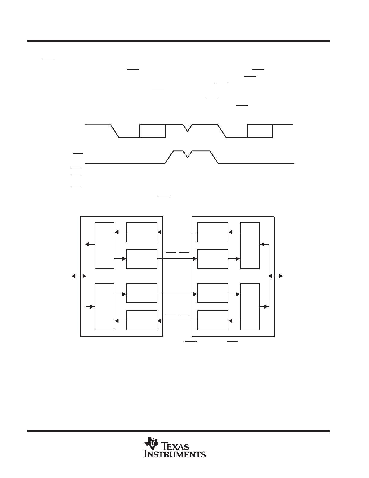
The transmitter circuitry checks CTS before sending the next data byte. When CTS is active, the transmitter
sends the next byte. To stop the transmitter from sending the following byte. CTS must be deasserted before
the middle of the last stop bit that is currently being sent. The auto-CTS function reduces interrupts to the host
system. When flow control is enabled, the CTS
device automatically controls its own transmitter. Without auto-CTS, the transmitter sends any data present in
the transmit FIFO and a receiver overrun error can result. Figure 2 shows CTS functional timing, and Figure 3
shows an example of autoflow control.
state changes and need not trigger host interrupts because the
TX
CTS
NOTES: A. When CTS is low, the transmitter keeps sending serial data out
B. When CTS
it does not send the next byte.
C. When CTS
goes high before the middle of the last stop bit of the current byte, the transmitter finishes sending the current byte but
goes from high to low, the transmitter begins sending data again.
Byte 0–7 StopStart Byte 0–7 StopStart
Figure 2. CTS Functional Timing
UART 1 UART 2
Serial to
Parallel
RX
FIFO
Flow
Control
D7–D0 D7–D0
Parallel to
Serial
TX
FIFO
Flow
Control
RX
RTS
TX
CTS
TX
CTS
RX
RTS
Parallel to
Serial
TX
FIFO
Flow
Control
Serial to
Parallel
RX
FIFO
Flow
Control
Figure 3. Autoflow Control (Auto-RTS and Auto-CTS) Example
6
POST OFFICE BOX 655303 • DALLAS, TEXAS 75265
TL16C752B
3.3-V DUAL UART WITH 64-BYTE FIFO
SLLS405 – DECEMBER 1999
functional description (continued)
software flow control
Software flow control is enabled through the enhanced feature register and the modem control register. Different
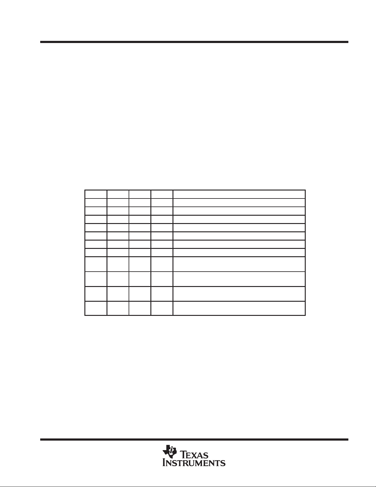
combinations of software flow control can be enabled by setting different combinations of EFR[3–0]. Table 1
shows software flow control options.
There are two other enhanced features relating to S/W flow control:
– Xon Any Function [MCR(5)]: Operation will resume after receiving any character after recognizing the
Xoff character.
NOTE:
It is possible that an Xon1 character is recognized as an Xon Any character which could cause an
Xon2 character to be written to the RX FIFO.
– Special Character [EFR(5)]: Incoming data is compared to Xoff2. Detection of the special character
sets the Xoff interrupt {IIR(4)] but does not halt transmission. The Xoff interrupt is cleared by a read of the
IIR. The special character is transferred to the R FIFO.
Table 1. Software Flow Control Options EFR[0:3]
BIT 3 BIT 2 BIT 1 BIT 0 Tx, Rx SOFTWARE FLOW CONTROLS
0 0 X X No transmit flow control
1 0 X X Transmit Xon1, Xoff1
0 1 X X Transmit Xon2, Xoff2
1 1 X X Transmit Xon1, Xon2: Xoff1, Xoff2
X X 0 0 No receive flow control
X X 1 0 Receiver compares Xon1, Xoff1
X X 0 1 Receiver compares Xon2, Xoff2
1 0 1 1 Transmit Xon1, Xoff1
0 1 1 1 Transmit Xon2, Xoff2
1 1 1 1 Transmit Xon1, Xon2: Xoff1, Xoff2
0 0 1 1 No transmit flow control
Receiver compares Xon1 and Xon2, Xoff1 and Xoff2
Receiver compares Xon1 and Xon2, Xoff1 and Xoff2
Receiver compares Xon1 and Xon2: Xoff1 and Xoff2
Receiver compares Xon1 and Xon2: Xoff1 and Xoff2
RX
When software flow control operation is enabled, the TL16C752B will compare incoming data with Xoff1/2
programmed characters (in certain cases Xoff1 and Xoff2 must be received sequentially1). When the correct
Xoff characters are received, transmission is halted after completing transmission of the current character . Xoff
detection also sets IIR[4] (if enabled via IER[5]) and causes INT to go high.
To resume transmission an Xon1/2 character must be received (in certain cases Xon1 and Xon2 must be
received sequentially). When the correct Xon characters are received IIR[4] is cleared and the Xoff interrupt
disappears.
NOTE:
If a parity, framing or break error occurs while receiving a software flow control character, this
character will be treated as normal data and will be written to the RCV FIFO.
1. When pairs of Xon/Xoff characters are programmed to occur sequentially, received Xon1/Xoff1 characters must be written to the Rx FIFO
if the subsequent character is not Xon2/Xoff2.
POST OFFICE BOX 655303 • DALLAS, TEXAS 75265
7
TL16C752B
3.3-V DUAL UART WITH 64-BYTE FIFO
SLLS405 – DECEMBER 1999
functional description (continued)
TX
Xoff1/2 characters are transmitted when the RX FIFO has passed the programmed trigger level TCR[3:0].
Xon1/2 characters are transmitted when the RX FIFO reaches the trigger level programmed via TCR[7:4].
An important note here is that if, after an xoff character has been sent and software flow control is disabled, the
UART will transmit Xon characters automatically to enable normal transmission to proceed. A feature of the
TL16C752B UART design is that if the software flow combination (EFR[3:0]) changes after an Xoff has been
sent, the originally programmed Xon is automatically sent. If the RX FIFO is still above the trigger level, the newly
programmed Xoff1/2 will be transmitted.
The transmission of Xoff/Xon(s) follows the exact same protocol as transmission of an ordinary byte from the
FIFO. This means that even if the word length is set to be 5, 6, or 7 characters then the 5, 6, or 7 least significant
bits of Xoff1,2/Xon1,2 will be transmitted. (Note that the transmission of 5, 6, or 7 bits of a character is seldom
done, but this functionality is included to maintain compatibility with earlier designs.)
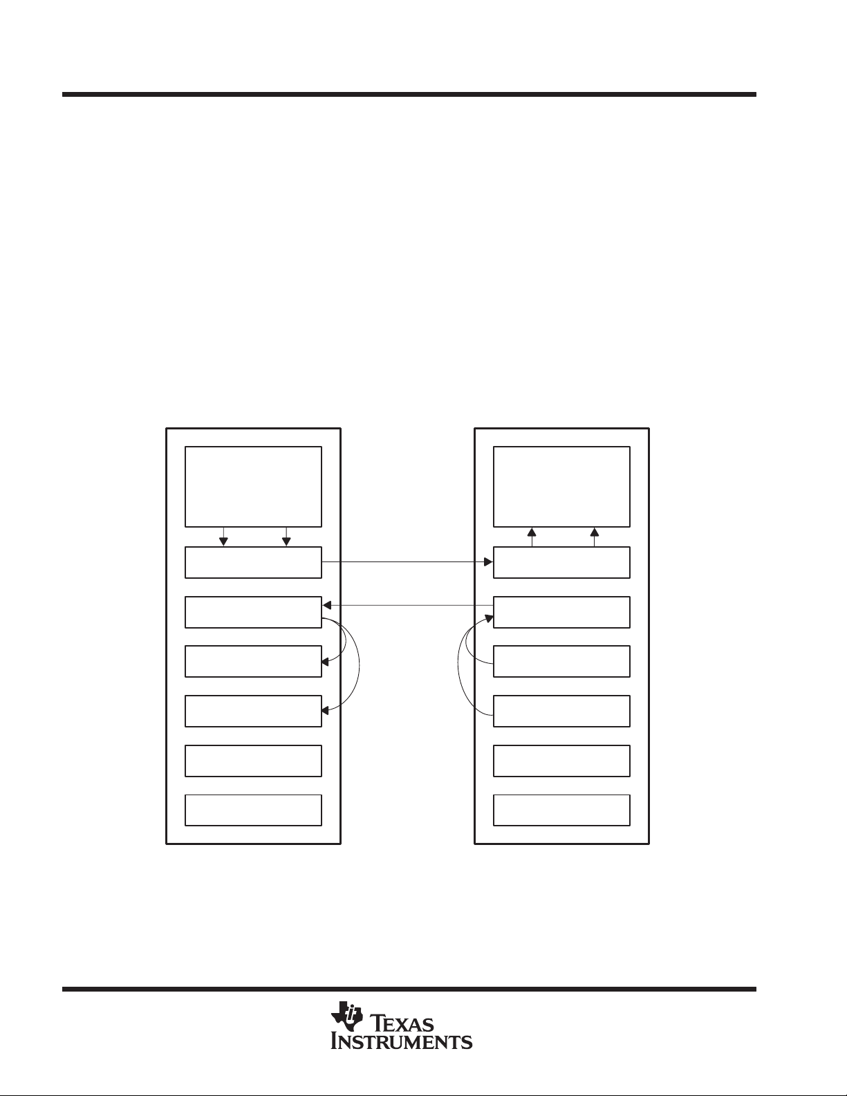
It is assumed that software flow control and hardware flow control will never be enabled simultaneously . Figure 4
shows an example of software flow control.
UART 1
UART 2
Transmit
FIFO
Parallel to Serial
Serial to Parallel
Xon-1 Word
Xon-2 Word
Xoff-1 Word
Xoff-1 Word
Figure 4. Software Flow Control Example
Data
Xoff – Xon – Xoff
Compare
Programmed
Xon–Xoff
Characters
Receive
FIFO
Serial to Parallel
Parallel to Serial
Xon-1 Word
Xon-2 Word
Xoff-1 Word
Xoff-2 Word
8
POST OFFICE BOX 655303 • DALLAS, TEXAS 75265
TL16C752B
3.3-V DUAL UART WITH 64-BYTE FIFO
SLLS405 – DECEMBER 1999
functional description (continued)
software flow control example
Assumptions: UART1 is transmitting a large text file to UART2. Both UART s are using software flow control with
single character Xoff (0F) and Xon (0D) tokens. Both have Xoff threshold (TCR [3:0]=F) set to 60 and Xon
threshold (TCR[7:4]=8) set to 32. Both have the interupt receive threshold (TLR[7:4]=D) set to 52.
UART1 begins transmission and sends 52 characters, at which point UART2 will generate an interrupt to its
processor to service the RCV FIFO, but assume the interrupt latency is fairly long. UART1 will continue sending
characters until a total of 69 characters have been sent. At this time UART2 will transmit a 0F to UART1,
informing UART1 to halt transmission. UART1 will likely send the 61
Xoff character . Now UART2 is serviced and the processor reads enough data out of the RCV FIFO that the level
drops to 32. UART2 will now send a 0D to UART1, informing UART1 to resume transmission.
reset
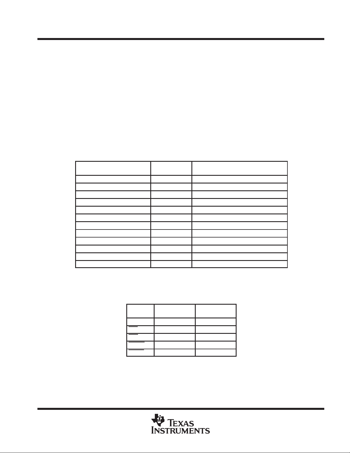
Table 2 summarizes the state of registers after reset.
Table 2. Register Reset Functions
st
character while UART2 is sending the
REGISTER
Interrupt enable register RESET All bits cleared
Interrupt identification register RESET Bit 0 is set. All other bits cleared.
FIFO control register RESET All bits cleared
Line control register RESET Reset to 00011101 (1D hex).
Modem control register RESET All bits cleared
Line status register RESET Bits 5 and 6 set. All other bits cleared.
Modem status register RESET Bits 0–3 cleared. Bits 4–7 input signals.
Enhanced feature register RESET All bits cleared
Receiver holding register RESET Pointer logic cleared
Transmitter holding register RESET Pointer logic cleared
Transmission control register RESET All bits cleared
Trigger level register RESET All bits cleared
NOTE: Registers DLL, DLH, SPR, Xon1, Xon2, Xoff1, Xoff2 are not reset by the top-level reset signal
RESEST, i.e., they hold their initialization values during reset.
RESET
CONTROL
Table 3 summarizes the state of registers after reset.
Table 3. Signal Reset Functions
SIGNAL
TX RESET High
RTS RESET High
DTR RESET High
RXRDY RESET High
TXRDY RESET Low
RESET
CONTROL
RESET STATE
RESET STATE
interrupts
The TL16C752B has interrupt generation and prioritization (6 prioritized levels of interrupts) capability. The
iInterrupt enable register (IER) enables each of the 6 types of interrupts and the INT signal in response to an
interrupt generation. The IER can also disable the interrupt system by clearing bits 0–3, 5–7. When an interrupt
is generated, the IIR indicates that an interrupt is pending and provides the type of interrupt through IIR[5–0].
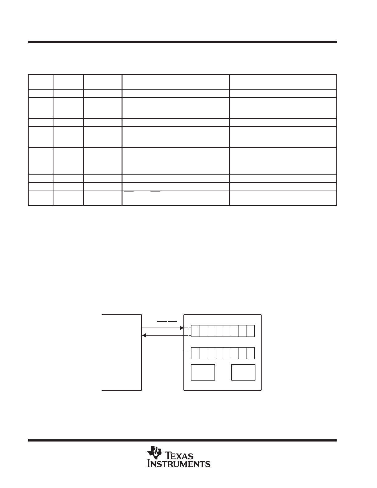
Table 4 summarizes the interrupt control functions.
POST OFFICE BOX 655303 • DALLAS, TEXAS 75265
9
TL16C752B
3.3-V DUAL UART WITH 64-BYTE FIFO
SLLS405 – DECEMBER 1999
functional description (continued)
Table 4. Interrupt Control Functions
IIR[5–0]
000001 None None None None
0001 10 1 Receiver line
001100 2 RX timeout Stale data in RX FIFO Read RHR
000100 2 RHR interrupt DRDY (data ready)
000010 3 THR interrupt TFE (THR empty)
000000 4 Modem status MSR[3:0] = 0 Read MSR
010000 5 Xoff interrupt Receive Xoff character(s)/special character Receive Xon character(s)/Read of IIR
100000 6 CTS, RTS RTS pin or CTS pin change state from active
PRIORITY
LEVEL
INTERRUPT
TYPE
status
INTERRUPT SOURCE INTERRUPT RESET METHOD
OE, FE, PE, or BI errors occur in characters in
the RX FIFO
(FIFO disable)
RX FIFO above trigger level (FIFO enable)
(FIFO disable)
TX FIFO passes above trigger level (FIFO
enable)
(low) to inactive (high)
FE< PE< BI: All erroneous characters are read
from the RX FIFO.
OE: Read LSR
Read RHR
Read IIR OR a write to the THR
Read IIR
It is important to note that for the framing error, plarity error , and break conditions, LSR[7] generates the interrupt.
LSR[7] is set when there is an error anywhere in the RX FIFO and is cleared only when there are no more errors
remaining in the FIFO. LSR[4–2] always represent the error status for the received character at the top of the
RX FIFO. Reading the RX FIFO updates LSR[4–2] to the appropriate status for the new character at the top
of the FIFO. If the Rx FIFO is empty, then LSR[4–2] is all zeros.
For the Xoff interrupt, if an Xoff flow character detection caused the interrupt, the interrupt is cleared by an Xon
flow character detection. If a special character detection caused the interrupt, the interrupt is cleared by a read
of the LSR.
interrupt mode operation
In interrupt mode (if any bit of IER[3:0] is 1) the processor is informed of the status of the receiver and transmitter
by an interrupt signal, INT . Therefore, it is not necessary to continuously poll the line stats register (LSR) to see
if any interrupt needs to be serviced. Figure 5 shows interrupt mode operation.
IOW/IOR
INTProcessor
THR RHR
IER
1111
IIR
Figure 5. Interrupt Mode Operation
10
POST OFFICE BOX 655303 • DALLAS, TEXAS 75265
TL16C752B
3.3-V DUAL UART WITH 64-BYTE FIFO
SLLS405 – DECEMBER 1999
functional description (continued)
polled mode operation
In polled mode (IER[3:0]=0000) the status of the receiver and transmitter can then be checked by polling the
line status register (LSR). This mode is an alternative to the FIFO interrupt mode of operation where the status
of the receiver and transmitter is automatically known by means of interrupts sent to the CPU. Figure 6 shows
FIFO polled mode operation.
IOW/IOR
Processor
THR RHR
LSR
IER
0000
Figure 6. FIFO Polled Mode Operation
DMA signalling
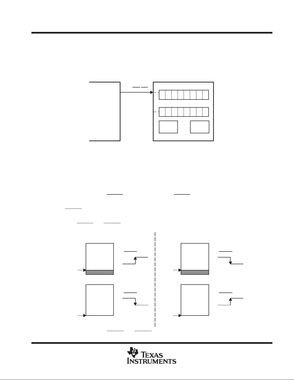
There are two modes of DMA operation: DMA mode 0 or 1, selected by FCR[3].
In DMA mode 0 or FIFO disable (FCR[0]=0) DMA occurs in single character transfers. In DMA mode 1 multi-
character (or block) DMA transfers are managed to relieve the processor for longer periods of time.
single DMA transfers (DMA mode0/FIFO disable)
Transmitter: When empty, the TXRDY signal becomes active. TXRDY will go inactive after one character has
been loaded into it.
Receiver: RXRDY is active when there is at least one character in the FIFO. It becomes inactive when the
receiver is empty.
Figure 7 shows TXRDY and RXRDY in DMA mode0/FIFO disable.
TX
TXRDY
wrptr
wrptr
At Least One
Location Filled
TXRDY
FIFO Empty
rdptr
rdptr
Figure 7. TXRDY and RXRDY in DMA Mode 0/FIFO Disable
RX
RXRDY
At Least One
Location Filled
RXRDY
FIFO Empty
POST OFFICE BOX 655303 • DALLAS, TEXAS 75265
11
 Loading...