

查询TL16C552A供应商
D
IBM PC/A T Compatible
D
Two TL16C550 ACEs
D
Enhanced Bidirectional Printer Port
D
16-Byte FIFOs Reduce CPU Interrupts
D
Up to 16-MHz Clock Rate for up to 1-Mbaud
Operation
D
Transmit, Receive, Line Status, and Data
Set Interrupts on Each Channel
Independently Controlled
D
Individual Modem Control Signals for Each
Channel
RXRDY0
DCD1
GND
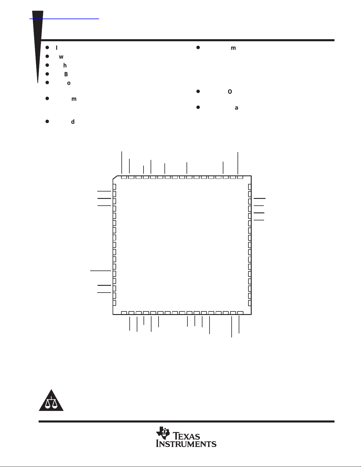
TL16C552A, TL16C552AM
DUAL ASYNCHRONOUS COMMUNICATIONS ELEMENT
WITH FIFO
SLLS189D – NOVEMBER 1994 – REVISED JANUARY 1999
D
Programmable Serial Interface
Characteristics for Each Channel:
– 5-, 6-, 7-, or 8-Bit Characters
– Even, Odd, or No Parity Bit Generation
and Detection
– 1-, 1-1/2-, or 2-Stop Bit Generation
D
3-State Outputs Provide TTL Drive for the
Data and Control Bus on Each Channel
D
Hardware and Software Compatible With
TL16C452
HV or FN PACKAGE
(TOP VIEW)
DD
ERR
SIN1
RI1
DSR1
CLK
CS1
TRI
ACK
PEMD
PE
BUSY
SLCT
V
RXRDY1
SOUT1
DTR1
RTS1
CTS1
DB0
DB1
DB2
DB3
DB4
DB5
DB6
DB7
TXRDY0
V
DD
RTS0
DTR0
SOUT0
87 65493
10
11
12
13
14
15
16
17
18
19
20
21
22
23
24
25
26
27
28 29
GND
CTS0
DCD0
31 32 33 34
30
RI0
DSR0
A2A1A0
CS0
168672
35 36 37 38 39
IOW
66 65
IOR
CS2
64 63 62 61
40 41 42 43
DD
V
SIN0
RESET
60
59
58
57
56
55
54
53
52
51
50
49
48
47
46
45
44
ENIRQ
TXRDY1
INT1
INT2
SLIN
INIT
AFD
STB
GND
PD0
PD1
PD2
PD3
PD4
PD5
PD6
PD7
INT0
BDO
Please be aware that an important notice concerning availability, standard warranty, and use in critical applications of
Texas Instruments semiconductor products and disclaimers thereto appears at the end of this data sheet.
IBM PC/AT is a trademark of International Business Machines Corporation.
PRODUCTION DATA information is current as of publication date.
Products conform to specifications per the terms of Texas Instruments
standard warranty. Production processing does not necessarily include
testing of all parameters.
POST OFFICE BOX 655303 • DALLAS, TEXAS 75265
Copyright 1999, Texas Instruments Incorporated
1
TL16C552A, TL16C552AM
DUAL ASYNCHRONOUS COMMUNICATIONS ELEMENT
WITH FIFO
SLLS189D – NOVEMBER 1994 – REVISED JANUARY 1999
PN PACKAGE
(TOP VIEW)
NC
NC
RXRDY1
SIN1
ERR
V
DD
SLCT
BUSY
PE
ACK
PEMD
TRI
CS1
CLK
DSR1
RI1
GND
DCD1
RXRDY0
NC
NC
INT1
79 78 77 76 7580 74
1
2
3
4
5
6
7
8
9
10
11
12
13
14
15
16
17
18
19
20
22 23
21
INT2
SLIN
25 26 27 28
24
INIT
AFD
STB
GND
PD0
72 71 7073
30 31 32 33
29
PD1
PD2
69 68
PD3
PD4
67 66 65 64
34 35 36 37
PD5
PD6
PD7
INT0
BDO
63 62 61
38 39 40
NC
NC
60
59
58
57
56
55
54
53
52
51
50
49
48
47
46
45
44
43
42
41
NC
ENIRQ
TXRDY1
SIN0
V
DD
RESET
CS2
IOR
IOW
A0
A1
A2
CS0
DSR0
RI0
DCD0
CTS0
GND
NC
NC
NC
NC
DTR1
SOUT1
RTS1
DB0
CTS1
DB1
DB2
DB3
DB4
DB5
DB6
DB7
TXRDY0
V
DD
RTS0
DTR0
SOUT0
NC
description
The TL16C552A is an enhanced dual-channel version of the popular TL16C550B asynchronous
communications element (ACE). The device serves two serial input/output interfaces simultaneously in
microcomputer or microprocessor-based systems. Each channel performs serial-to-parallel conversion on data
characters received from peripheral devices or modems and parallel-to-serial conversion on data characters
transmitted by the CPU. The complete status of each channel of the dual ACE can be read at any time during
functional operation by the CPU. The information obtained includes the type and condition of the transfer
operations being performed and the error conditions encountered.
In addition to its dual communications interface capabilities, the TL16C552A provides the user with a
bidirectional parallel data port that fully supports the parallel Centronics-type printer interface. The parallel port
and the two serial ports provide IBM PC/A T-compatible computers with a single device to serve the three system
ports. A programmable baud rate generator that can divide the timing reference clock input by a divisor between
1 and (2
The TL16C552A is available in a 68-pin plastic-leaded chip-carrier (FN) package, a 48-pin TQFP (PN) package,
and the 80-pin TQFP (PN) package. The TL16C552AM is available in a 68-pin ceramic quad flat (HV) package.
16
– 1) is included.
2
POST OFFICE BOX 655303 • DALLAS, TEXAS 75265
functional block diagram
TL16C552A, TL16C552AM
DUAL ASYNCHRONOUS COMMUNICATIONS ELEMENT
WITH FIFO
SLLS189D – NOVEMBER 1994 – REVISED JANUARY 1999
A0–A2
IOW
IOR
RESET
CLK
35–33
36
37
39
4
CTS0
DSR0
DCD0
RI0
SIN0
CS0
DB0–DB7
CTS1
DSR1
DCD1
RI1
SIN1
CS1
3
ERR
SLCT
BUSY
PE
ACK
PEMD
CS2
ENIRQ
28
31
29
30
41
32
14–21
13
5
8
6
62
3
Select
and
Control
Logic
63
65
66
67
68
1
38
43
24
RTS0
25
DTR0
26
ACE
#1
8
8
ACE
#2
8
8
53–46
Parallel
Port
45
9
22
12
11
10
60
61
42
44
57
56
55
58
59
SOUT0
INT0
RXRDY0
TXRDY0
RTS1
DTR1
SOUT1
INT1
RXRDY1
TXRDY1
BDO
PD0–PD7
INIT
AFD
STB
SLIN
INT2
POST OFFICE BOX 655303 • DALLAS, TEXAS 75265
3
TL16C552A, TL16C552AM
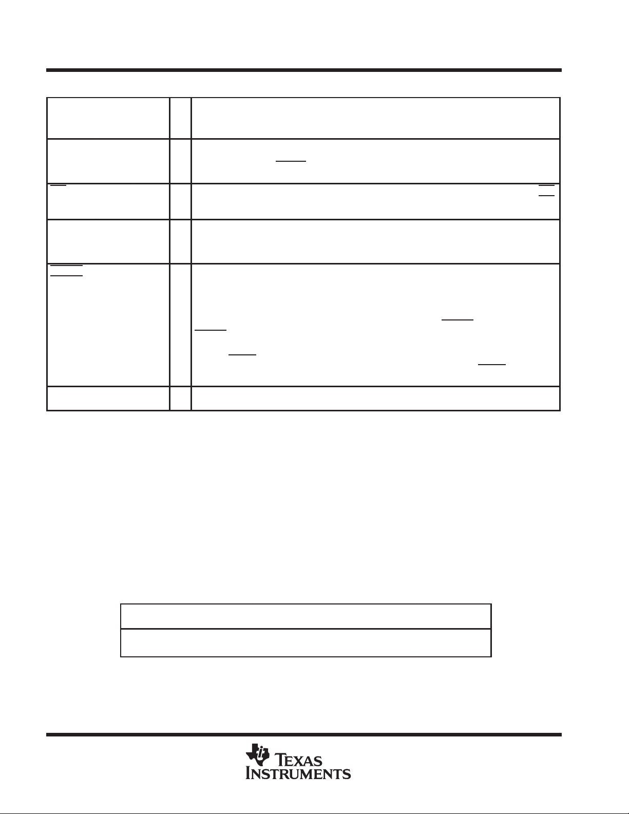
NAME
DUAL ASYNCHRONOUS COMMUNICATIONS ELEMENT
WITH FIFO
SLLS189D – NOVEMBER 1994 – REVISED JANUARY 1999
Terminal Functions
TERMINAL
DESCRIPTION
has an internal pullup resistor to VDD of
terminal has changed states
. When ENIRQ is tied high, the PS-2 mode of interrupt
bit in the line printer status register.
. INT2 is held until the status register is read, which then
has an internal pullup resistor to VDD of
73
I/O
generates a printer port interrupt during its positive transition.
Line printer autofeed. AFD is an open-drain line that provides the printer with an active-low signal when
continuous form paper is to be autofed to the printer. AFD
approximately 10 kΩ.
2 for the decode of the serial channels and Table 13 for the decode of the parallel printer port.
port is read. BDO controls the system bus driver (74LS245 or 54LS245).
to accept data.
Chip select. Each CSx input acts as an enable for the write and read signals for serial channels 1 (CS0)
and 2 (CS1
register (CTS is bit 4 of the modem status register, written as MSR4) of each ACE. A change of state
in either CTS
(MSR0) of each modem status register.
control, and status information between the TL16C552A and the CPU. These lines are normally in the
high-impedance state except during read operations. DB0 is the least significant bit (LSB) and is the
first serial data bit to be received or transmitted.
(DCD) of the modem status registers. MSR3 (∆DCD) of the modem status register indicates whether
DCD
Data set ready. The logical state of the DSRx terminals is reflected in MSR5 of its associated modem
status register. ∆DSR (MSR1) indicates whether the associated DSRx
since the previous reading of the MSR.
Data terminal ready. Each DTRx can be set low by setting MCR0, modem control register bit 0 of its
associated ACE. DTRx
When active (low), DTRx
In AT mode, INT2 is internally connected to ACK
is enabled and INT2 is internally tied to the inverse of the PRINT
INT2 is latched high on the rising edge of ACK
clears the PRINT
during the error condition.
Ground (0 V). All terminals must be tied to GND for proper operation.
allows the printer initialization routine to be started. INIT
approximately 10 kΩ.
MCR) goes active (high) when one of the following interrupts has an active (high) condition and is
enabled by the interrupt enable register of its associated channel: receiver error flag, received data
available, transmitter holding register empty , and modem status. The interrupt is cleared on appropriate
service. Upon reset, the interrupt output is in the high-impedance state.
). CS2 enables the signals to the printer port.
terminal since the previous reading of the associated MSR causes the setting of ∆CTS
has changed states since the previous reading of the MSR. DCD has no effect on the receiver.
is cleared (high) by clearing the DTR bit (MCR0) or whenever a reset occurs.
indicates that its ACE is ready to receive data.
status bit and INT2.
NO.
FN PN
ACK 68 10 I Line printer acknowledge. ACK goes low to indicate a successful data transfer has taken place. ACK
AFD 56 75 I/O
A0, A1, A2 35, 34,3351, 50,49I Address. The address lines A0–A2 select the internal registers during CPU bus operations. See T able
BDO 44 63 O Bus buffer. BDO is the active-high output and is asserted when either the serial channel or the parallel
BUSY 66 8 I Line printer busy. BUSY is an input line from the printer that goes high when the printer is not ready
CLK 4 14 I Clock. CLK is the external clock input to the baud rate divisor of each ACE.
CS0, CS1,
CS2
CTS0,
CTS1
DB0 –
DB7
DCD0,
DCD1
DSR0,
DSR1
DTR0,
DTR1
ENIRQ 43 59 I Parallel port interrupt source mode selection. When ENIRQ is low, the A T mode of interrupts is enabled.
ERR 63 5 I Line printer error. ERR is an input line from the printer. The printer reports an error by holding ERR low
GND 7, 27,5417, 43,
INIT 57 76 I/O Line printer initialize. INIT is an open-drain line that provides the printer with an active-low signal that
INT0, INT1 45, 60 64, 79 O External serial channel interrupt. Each serial channel interrupt 3-state output (enabled by bit 3 of the
32, 3,3848, 13,54I
28, 13 44, 26 I Clear to send. The logical state of each CTSx terminal is reflected in the CTS bit of the modem status
14 – 21 27 – 34 I/O Data bits DB0–DB7. The data bus provides eight I/O lines with 3-state outputs for the transfer of data,
29, 8 45, 18 I Data carrier detect. DCD is a modem input. Its condition can be tested by the CPU by reading MSR7
31, 5 47, 15 I
25, 11 38, 24 O
4
POST OFFICE BOX 655303 • DALLAS, TEXAS 75265

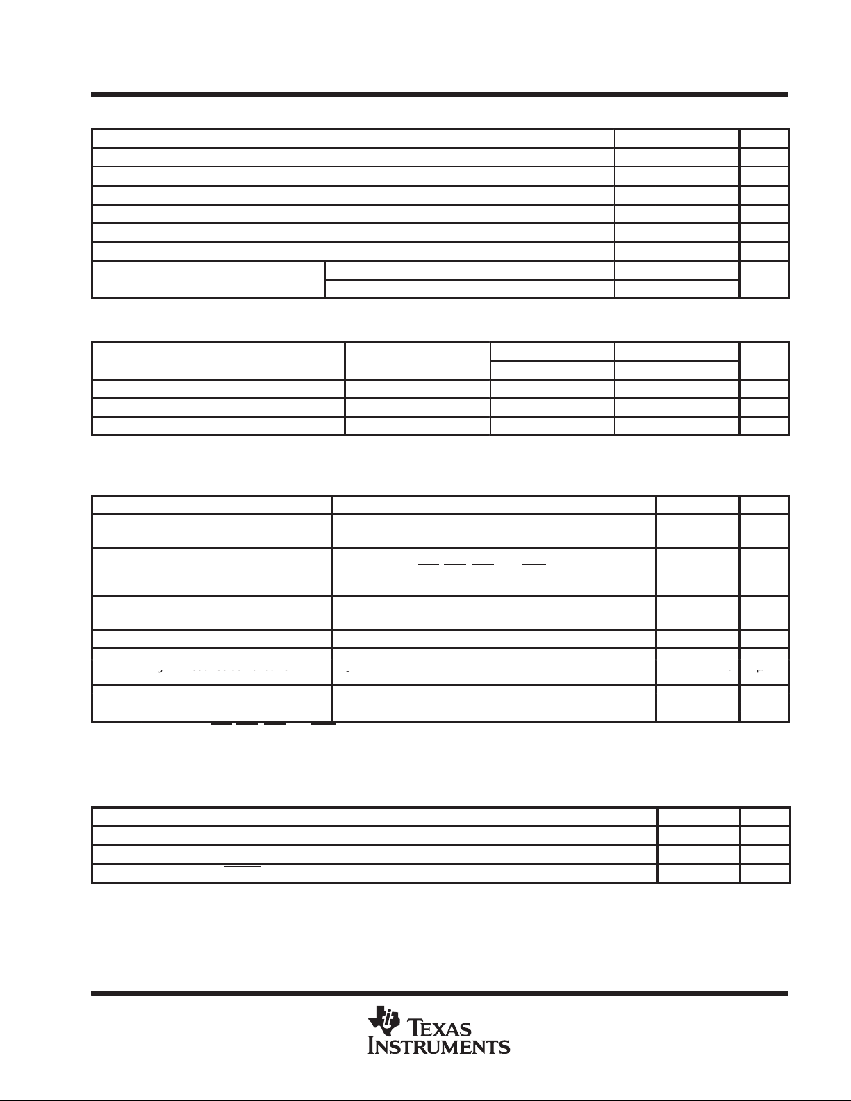
TL16C552A, TL16C552AM
NAME
DUAL ASYNCHRONOUS COMMUNICATIONS ELEMENT
WITH FIFO
SLLS189D – NOVEMBER 1994 – REVISED JANUARY 1999
Terminal Functions (Continued)
TERMINAL
NO.
FN PN
INT2 59 78 O Printer port interrupt. INT2 is an active-high, 3-state output generated by the positive transition of
IOR 37 53 I Input/output read strobe. IOR is an active-low input that enables the selected channel to output data
IOW 36 52 I Input/output write strobe. IOW is an active-low input causing data from the data bus to be input to either
PD0–PD7 53–46 72–65 I/O Parallel data bits (0–7). PD0–PD7 provide a byte wide input or output port to the system.
PE 67 9 I Line printer paper empty. PE is an input line from the printer that goes high when the printer runs out
PEMD 1 11 I Printer enhancement mode. When low, PEMD enables the write data register to the PD0–PD7 lines.
RESET 39 55 I Reset. When low, RESET forces the TL16C552A into an idle mode in which all serial data activities
RTS0,
RTS1
RXRDY0,
RXRDY1
RI0, RI1 30, 6 46, 16 I Ring indicator. The RI signal is a modem control input. Its condition is tested by reading MSR6 (RI) of
SIN0,
SIN1
SLCT 65 7 I Line printer select. SLCT is an input line from the printer that goes high when the printer is selected.
SLIN 58 77 I/O Line printer select. SLIN is an open-drain I/O that selects the printer when active (low). SLIN has an
24, 12 37, 25 O Request to send. The RTS outputs are set low by setting MCR1 of its UARTs modem control register .
9, 61 19, 3 O
41, 62 57, 4 I Serial data. SIN0 and SIN1 move information from the communication line or modem to the
I/O
ACK
. INT2 is enabled by bit 4 of the write control register. Upon reset, INT2 is in the high-impedance
state. Its mode is also controlled by ENIRQ
to the data bus (DB0–DB7). The data output depends on the register selected by the address inputs
A0, A1, A2, and chip select. Chip select 0 (CS0
and chip select 2 (CS2
ACE or to the parallel port. The destination depends on the register selected by the address inputs A0,
A1, A2, and chip selects CS0
of paper.
A high on PEMD allows direction control of the PD0–PD7 port by the DIR bit in the control register.
PEMD is usually tied low for the printer operation.
are suspended. The modem control register and its associated outputs are cleared. The line status
register is cleared except for the transmitter holding register empty (THRE) and TEMT bits, which are
set. All functions of the device remain in an idle state until programmed to resume serial data activities.
RESET
has a hysteresis level of typically 400 mV.
Both RTS
transmit. In half-duplex operations, RTS
Receiver ready. Receiver direct memory access (DMA) signaling is also available through this output.
One of two types of DMA signaling can be selected using FCR3 when in FIFO mode. Only DMA mode
0 is allowed when in TL16C450 mode. For signal transfer DMA (a transfer is made between CPU bus
cycles), mode 0 is used. Multiple transfers that are made continuously until the receiver FIFO has been
emptied are supported by mode 1.
Mode 0. RXRDY is active (low) in FIFO mode (FCR0 = 1, FCR3 = 0) or in TL16C450 mode (FCR0 =
0) and the receiver FIFO or receiver holding register contains at least one character. When there are
no more characters in the FIFO or holding register, RXRDY
Mode 1. RXRDY goes active (low) in the FIFO mode (FCR0 = 1) when FCR3 = 1 and the time-out or
trigger levels have been reached. RXRDY
empty.
each ACE. The modem status register output TERI (MSR2) indicates whether RI
high to low since the previous reading of the modem status register.
TL16C552A receiver circuits. Mark is a high state and space is a low state. Data on serial data inputs
is disabled in loop mode.
internal pullup resistor to VDD of approximately 10 kΩ.
terminals are reset high by RESET. A low on RTS indicates that its ACE has data ready to
) selects the printer port.
, CS1, and CS2.
DESCRIPTION
.
) selects ACE #1, chip select 1 (CS1) selects ACE #2,
controls the direction of the line.
goes inactive (high).
goes inactive (high) when the FIFO or holding register is
has changed from
POST OFFICE BOX 655303 • DALLAS, TEXAS 75265
5
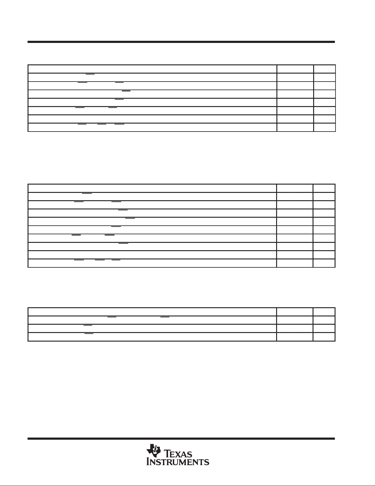
TL16C552A, TL16C552AM
NAME
DUAL ASYNCHRONOUS COMMUNICATIONS ELEMENT
WITH FIFO
SLLS189D – NOVEMBER 1994 – REVISED JANUARY 1999
Terminal Functions (Continued)
TERMINAL
DESCRIPTION
is active (low). Once
goes inactive
56
I/O
A mark is a high state and a space is a low state. Each SOUT is held in the mark condition when the
transmitter is disabled (RESET
mode.
is active (low), it provides the printer with a signal to latch the data currently on the parallel port. STB
has an internal pullup resistor to VDD of approximately 10 kΩ.
is asserted, all I/Os and outputs are in the high-impedance state, allowing board level testers to drive
the outputs without overdriving internal buffers. TRI is level sensitive and is pulled down with an internal
resistor that is approximately 5 kΩ.
operating in FIFO mode. Only DMA mode 0 is allowed when in TL16C450 mode. Single-transfer DMA
(a transfer is made between CPU bus cycles) is supported by mode 0. Multiple transfers that are made
continuously until the transmitter FIFO has been filled are supported by mode 1.
Mode 0. In FIFO mode (FCR0 = 1, FCR3 = 0) or in TL16C450 mode (FCR0 = 0) when there are no
characters in the transmitter holding register or transmitter FIFO, TXRDYx
TXRDYx
of the transmitter FIFO.
Mode 1. TXRDY goes active (low) in FIFO mode (FCR0 = 1) when FCR3 = 1 and there are no
characters in the transmitter FIFO. When the transmitter FIFO is completely full, TXRDY
(high).
Power supply. The VDD requirement is 5 V ±5%.
is activated (low), it goes inactive after the first character is loaded into the holding register
is asserted low), the transmitter register is empty, or when in the loop
NO.
FN PN
SOUT0,
SOUT1
STB 55 74 I/O Line printer strobe. STB provides communication between the TL16C552A and the printer. When STB
TRI 2 12 I 3-state output control input. TRI controls the 3-state control of all I/O and output terminals. When TRI
TXRDY0
TXRDY1
V
DD
26, 10 39, 23 O Serial data outputs. SOUT0 and SOUT1 are the serial data outputs from the ACE transmitter circuitry .
22, 42 35, 58 O Transmitter ready . T wo types of DMA signaling are available. Either can be selected using FCR3 when
23, 40,646, 36,
absolute maximum ratings over operating free-air temperature range (unless otherwise noted)
Supply voltage range, V
Input voltage range, V
Output voltage range, V
Continuous total power dissipation See Dissipation Rating Table. . . . . . . . . . . . . . . . . . . . . . . . . . . . . . . . . . . . .
Operating free-air temperature range, T
Storage temperature range, T
†
Stresses beyond those listed under “absolute maximum ratings” may cause permanent damage to the device. These are stress ratings only, and
functional operation of the device at these or any other conditions beyond those indicated under “recommended operating conditions” is not
implied. Exposure to absolute-maximum-rated conditions for extended periods may affect device reliability.
NOTE 1: All voltage levels are with respect to GND.
PACKAGE
FN 1730 mW 19.2 mW/°C 865 mW –
HV 1689 mW 13.5 mW/°C 1081 mW 337 mW
‡
Power ratings assume a maximum junction temperature (TJ) of 115°C for ’I’ and 150°C for ’M’ suffix devices.
§
Derating factor is the inverse of the junction-to-ambient thermal resistance, R
(see Note 1) –0.5 V to VDD + 0.3 V. . . . . . . . . . . . . . . . . . . . . . . . . . . . . . . . . . . . . .
DD
–0.5 V to 7 V. . . . . . . . . . . . . . . . . . . . . . . . . . . . . . . . . . . . . . . . . . . . . . . . . . . . . . . . . . . . . .
I
–0.5 V to VDD + 0.3 V. . . . . . . . . . . . . . . . . . . . . . . . . . . . . . . . . . . . . . . . . . . . . . . . . . .
O
: I suffix –40°C to 85°C. . . . . . . . . . . . . . . . . . . . . . . . . . . . . . . . . . . . .
A:
M suffix –55°C to 125°C. . . . . . . . . . . . . . . . . . . . . . . . . . . . . . . . . . . .
–65°C to 150°C. . . . . . . . . . . . . . . . . . . . . . . . . . . . . . . . . . . . . . . . . . . . . . . . . . .
stg
DISSIPATION RATING TABLE‡
TA ≤ 25°C
POWER RATING
DERATING FACTOR
ABOVE TA = 25°C
§
TA = 70°C
POWER RATING
TA = 125°C
POWER RATING
.
θJA
†
6
POST OFFICE BOX 655303 • DALLAS, TEXAS 75265
recommended operating conditions
Operating free-air temperature, T
°C
PARAMETER
TEST CONDITIONS
UNIT
V
DD
V
O
with chi deselected or
µ
IOZHigh im edance out ut current
V
5.25 V with chi
2)
±20
µA
V
No load
IDDSupply current
DD
50
mA
In uts at 0.8 V or 2 V
f
clock
MHz
Supply voltage, V
Clock high-level input voltage, V
Clock low-level input voltage, V
High-level input voltage, V
Low-level input voltage, V
Clock frequency, f
p
DD
clock
IH(CLK)
IL(CLK)
IH
IL
p
A
I suffix –40 85
M suffix –55 125
package thermal characteristics
R
Junction-to-ambient thermal impedance Board mounted, no air flow 52 74 °C/W
θJA
R
Junction-to-case thermal impedance 14 3 °C/W
θJC
T
Junction temperature 115 150 °C/W
J
TL16C552A, TL16C552AM
DUAL ASYNCHRONOUS COMMUNICATIONS ELEMENT
WITH FIFO
SLLS189D – NOVEMBER 1994 – REVISED JANUARY 1999
MIN NOM MAX UNIT
4.75 5 5.25 V
2 V
0 0.8 V
2 V
0 0.8 V
FN Package HV Package
MIN TYP MAX MIN TYP MAX
DD
DD
V
V
16 MHz
°
electrical characteristics over recommended ranges of operating free-air temperature and supply
voltage (unless otherwise noted)
PARAMETER TEST CONDITIONS MIN MAX UNIT
V
OH
V
OL
I
I
I
I(CLK)
I
NOTES: 2. Excluding INIT, AFD, STB, and SLIN. They are open-drain terminals with an internal pullup resistor to VDD of approximately 10 KΩ.
High-level output voltage
Low-level output voltage
Input current
Clock input current VI = 0 to 5.25 V ±10 µA
High-impedance output current
pp
3. Excluding the TRI input terminal. It contains an internal pulldown resistor of approximately 5 kΩ.
IOH = –12 mA for PD0–PD7,
IOH = –4 mA for all other outputs (see Note 2),
IOL = 12 mA for PD0–PD7,
IOL = 12 mA for INIT
IOL = 4 mA for all other outputs
VDD = 5.25 V (see Note 3),
All other terminals are floating
= 5.25 V,
=
O
= 5.25 V,
DD
p
, AFD, STB, and SLIN,
= 0
p and write mode selected (see Note
,
= 8
p
s on outputs,
2.4 V
0.4 V
±10 µA
±20
A
clock timing requirements over recommended ranges of operating free-air temperature and supply
voltage
MIN MAX UNIT
t
t
t
w1
w2
w3
Pulse duration, CLK ↑ (external clock) (see Figure 1) 31 ns
Pulse duration, CLK ↓ (external clock) (see Figure 1) 31 ns
Pulse duration, RESET 1000 ns
POST OFFICE BOX 655303 • DALLAS, TEXAS 75265
7
TL16C552A, TL16C552AM
DUAL ASYNCHRONOUS COMMUNICATIONS ELEMENT
WITH FIFO
SLLS189D – NOVEMBER 1994 – REVISED JANUARY 1999
read cycle timing requirements over recommended ranges of operating free-air temperature and
supply voltage (see Note 4 and Figure 4)
MIN MAX UNIT
t
w4
t
su1
t
su2
t
h1
t
h2
t
d1
t
d2
NOTES: 4. These parameters are not production tested.
write cycle timing requirements over recommended ranges of operating free-air temperature and
supply voltage (see Note 7 and Figure 5)
t
w5
t
su4
t
su5
t
su6
t
h3
t
h4
t
h5
t
d3
t
d4
NOTES: 7. These parameters are not production tested.
Pulse duration, IOR ↓ 80 ns
Setup time, CSx valid before IOR ↓ (see Note 5) 15 ns
Setup time, A2–A0 valid before IOR ↓ (see Note 5) 15 ns
Hold time, A2–A0 valid after IOR ↑ (see Note 5) 20 ns
Hold time, CSx valid after IOR ↑ (see Note 5) 20 ns
Delay time, t
Delay time, IOR ↑ to IOR or IOW ↓ 80 ns
5. The internal address strobe is always active.
6. In FIFO mode, td1 = 425 ns (min) between reads of the receiver FIFO and the status registers (interrupt identification register and
line status register).
Pulse duration, IOW ↓ 80 ns
Setup time, CSx valid before IOW ↓ (see Note 8) 15 ns
Setup time, A2–A0 valid before IOW ↓ (see Note 8) 15 ns
Setup time, DB0–DB7 valid before IOW ↑ 15 ns
Hold time, A2–A0 valid after IOW ↑ (see Note 8) 20 ns
Hold time, CSx valid after IOW ↑ (see Note 8) 20 ns
Hold time, DB0–DB7 valid after IOW ↑ 15 ns
Delay time, t
Delay time, IOW ↑ to IOW or IOR ↓ 80 ns
8. The internal address strobe is always active.
+ tw4 + td2 (see Note 6) 175 ns
su2
MIN MAX UNIT
su5
+ tw5 + t
d4
175 ns
read cycle switching characteristics over recommended ranges of operating free-air temperature
and supply voltage, C
t
Propagation delay time from IOR ↓ to BDO ↑ or from IOR ↑ to BDO ↓ 60 ns
pd1
t
Enable time from IOR ↓ to DB0–DB7 valid (see Note 10) 60 ns
en
t
Disable time from IOR ↑ to DB0–DB7 released (see Note 10) 60 ns
dis
NOTES: 9. These parameters are not production tested.
8
10. VOL and VOH (and the external loading) determine the charge and discharge time.
= 100 pF (see Note 9 and Figure 4)
L
PARAMETER MIN MAX UNIT
POST OFFICE BOX 655303 • DALLAS, TEXAS 75265
TL16C552A, TL16C552AM
DUAL ASYNCHRONOUS COMMUNICATIONS ELEMENT
WITH FIFO
SLLS189D – NOVEMBER 1994 – REVISED JANUARY 1999
transmitter switching characteristics over recommended ranges of operating free-air temperature
and supply voltage (see Note 11 and Figures 6, 7, and 8)
PARAMETER TEST CONDITIONS MIN MAX UNIT
t
Delay time, interrupt THRE ↓ to SOUT ↓ at start See Figure 6 8 24
d5
t
Delay time, SOUT ↓ at start to interrupt THRE ↑ See Note 12 and Figure 6 8 9
d6
t
Delay time, IOW (WR THR) ↑ to interrupt THRE ↑ See Note 12 and Figure 6 16 32
d7
t
Delay time, SOUT ↓ at start to TXRDY ↓
d8
t
Propagation delay time from IOW (WR THR) ↓ to interrupt THRE ↓
pd2
t
Propagation delay time from IOR (RD IIR) ↑ to interrupt THRE ↓
pd4
t
Propagation delay time from IOW (WR THR) ↑ to TXRDY ↑
pd5
NOTES: 11. These parameters are not production tested.
12. When the transmitter interrupt delay is active, this delay is lengthened by one character time minus the last stop bit time.
CL = 100 pF,
See Figures 7 and 8
CL = 100 pF,
See Figure 6
CL = 100 pF,
See Figure 6
CL = 100 pF,
See Figures 7 and 8
RCLK
cycles
RCLK
cycles
RCLK
cycles
RCLK
8
cycles
140 ns
140 ns
195 ns
receiver switching characteristics over recommended ranges of operating free-air temperature
and supply voltage (see Note 13 and Figures 9 through 13)
PARAMETER TEST CONDITIONS MIN MAX UNIT
t
Delay time from stop to INT ↑ See Note 14 1
d9
t
Propagation delay time from RCLK ↑ to sample CLK ↑ 100 ns
pd6
t
Propagation delay time from IOR (RD RBR/RD LSR) ↓ to reset interrupt ↓ CL = 100 pF 150 ns
pd7
t
Propagation delay time from IOR (RD RBR) ↓ to RXRDY ↑ 150 ns
pd8
NOTES: 13. These parameters are not production tested.
14. The receiver data available indicator, the overrun error indicator, the trigger level interrupts, and the active RXRDY
delayed three RCLK cycles in FIFO mode (FCR0 = 1). After the first byte has been received, status indicators (PE, FE, BI) are
delayed three RCLK cycles. These indicators are updated immediately for any further bytes received after RDRBR goes active.
There are eight RCLK cycle delays for trigger change level interrupts.
RCLK
cycle
indicator are
modem control switching characteristics over recommended ranges of operating free-air
temperature and supply voltage, C
t
Propagation delay time from IOW (WR MCR) ↑ to RTS (DTR) ↓↑ 100 ns
pd9
t
Propagation delay time from modem input (CTS, DSR) ↓↑ to interrupt ↑ 170 ns
pd10
t
Propagation delay time from IOR (RD MSR) ↑ to interrupt ↓ 140 ns
pd11
t
Propagation delay time from RI ↑ to interrupt ↑ 170 ns
pd12
NOTE 15: These parameters are not production tested.
= 100 pF (see Note 15 and Figure 14)
L
PARAMETER MIN MAX UNIT
POST OFFICE BOX 655303 • DALLAS, TEXAS 75265
9
TL16C552A, TL16C552AM
DUAL ASYNCHRONOUS COMMUNICATIONS ELEMENT
WITH FIFO
SLLS189D – NOVEMBER 1994 – REVISED JANUARY 1999
parallel port timing requirements over recommended ranges of supply voltage and operating
free-air temperature (see Note 16 and Figures 15, 16, and 17)
MIN MAX UNIT
t
su7
t
h6
t
w6
t
d10
t
d11
t
w7
t
w8
t
d12
t
d13
t
d14
t
d15
t
d16
NOTES: 16. These parameters are not production tested.
Setup time, data valid before STB ↓ 1 µs
Hold time, data valid after STB ↑ 1 µs
Pulse duration, STB ↓ 1 µs
Delay time, BUSY ↑ to ACK ↓ Defined by printer
Delay time, BUSY ↓ to ACK ↓ Defined by printer
Pulse duration, BUSY ↑ Defined by printer
Pulse duration, ACK ↓ Defined by printer
Delay time, BUSY ↑ after STB ↑ Defined by printer
Delay time, INT2 ↓ after ACK ↓ (see Note 17) 22 ns
Delay time, INT2 ↑ after ACK ↑ (see Note 17) 20 ns
Delay time, INT2 ↑ after ACK ↑ (see Note 17) 24 ns
Delay time, INT2 ↓ after IOR ↑ (see Note 17) 25 ns
17. t
d13–td16
are all measured with a 15-pF load.
PARAMETER MEASUREMENT INFORMATION
t
w1
CLK (XTAL1)
f
clock
2 V
0.8 V
t
w2
= 16 MHz MAX
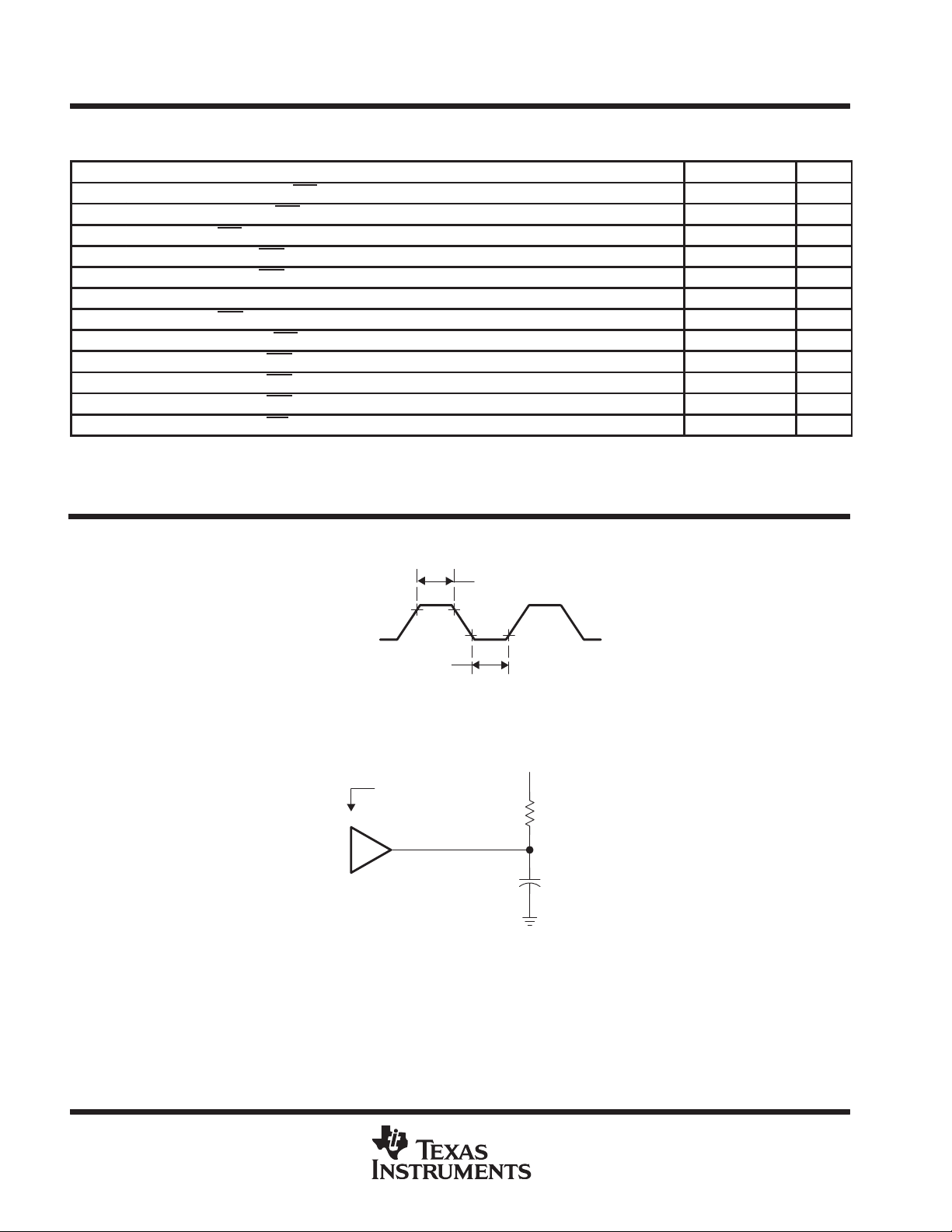
Figure 1. CLK Voltage Waveform
2.54 V
Device Under T est
TL16C552A
NOTE A: This includes scope and jig capacitance.
Figure 2. Output Load Circuit
2 V
0.8 V
680 Ω
82 pF
(see Note A)
10
POST OFFICE BOX 655303 • DALLAS, TEXAS 75265
TL16C552A, TL16C552AM
DUAL ASYNCHRONOUS COMMUNICATIONS ELEMENT
SLLS189D – NOVEMBER 1994 – REVISED JANUARY 1999
PARAMETER MEASUREMENT INFORMATION
TL16C552A
WITH FIFO
A2, A1, A0
, CS1, CS2
CS0
Data Bus
Address Bus
Control Bus
Serial
Channel 1
Buffers
Dual
ACE and
Printer
Port
Option
Jumpers
Serial
Channel 2
Buffers
Parallel
Port
R/C
Network
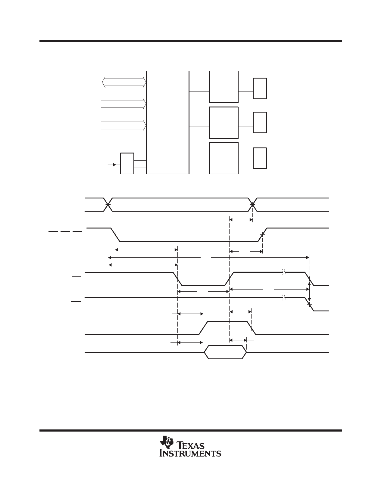
Figure 3. Basic Test Configuration
50% 50%
50% 50%
t
su1
t
su2
Valid
Valid
t
h1
t
t
d1
h2
9-Pin D Connector
9-Pin D Connector
25-Pin D Connector
IOR
IOW
BDO
DB0–DB7
Active
50% 50%
t
w4
t
pd1
50% 50%
t
en
Valid Data
Figure 4. Read Cycle Timing Waveforms
t
dis
t
pd1
50%
t
d2
50%
Active
or
Active
POST OFFICE BOX 655303 • DALLAS, TEXAS 75265
11
TL16C552A, TL16C552AM
DUAL ASYNCHRONOUS COMMUNICATIONS ELEMENT
WITH FIFO
SLLS189D – NOVEMBER 1994 – REVISED JANUARY 1999
PARAMETER MEASUREMENT INFORMATION
A2, A1, A0
CS0, CS1, CS2
DB0–DB7
Serial Out
(SOUT)
Interrupt
(THRE)
IOW
(WR THR)
t
pd2
IOW
IOR
50% 50%
50% 50%
t
su4
t
su5
Valid
Valid
t
d3
Active
50% 50%
t
w5
t
su6
Valid Data
t
h3
t
h4
50%
t
d4
50%
t
h5
Active
or
Active
Figure 5. Write Cycle Timing Waveforms
50%
t
d5
50%50%
Start
50% 50% 50%
t
d7
50%
Data Bits 5–8
t
50%
Stop (1–2)
Parity
pd2
Start
50%
t
d6
50%
t
pd4
12
IOR
(RD IIR)
IOW
(WR THR)
SOUT
TXRDY
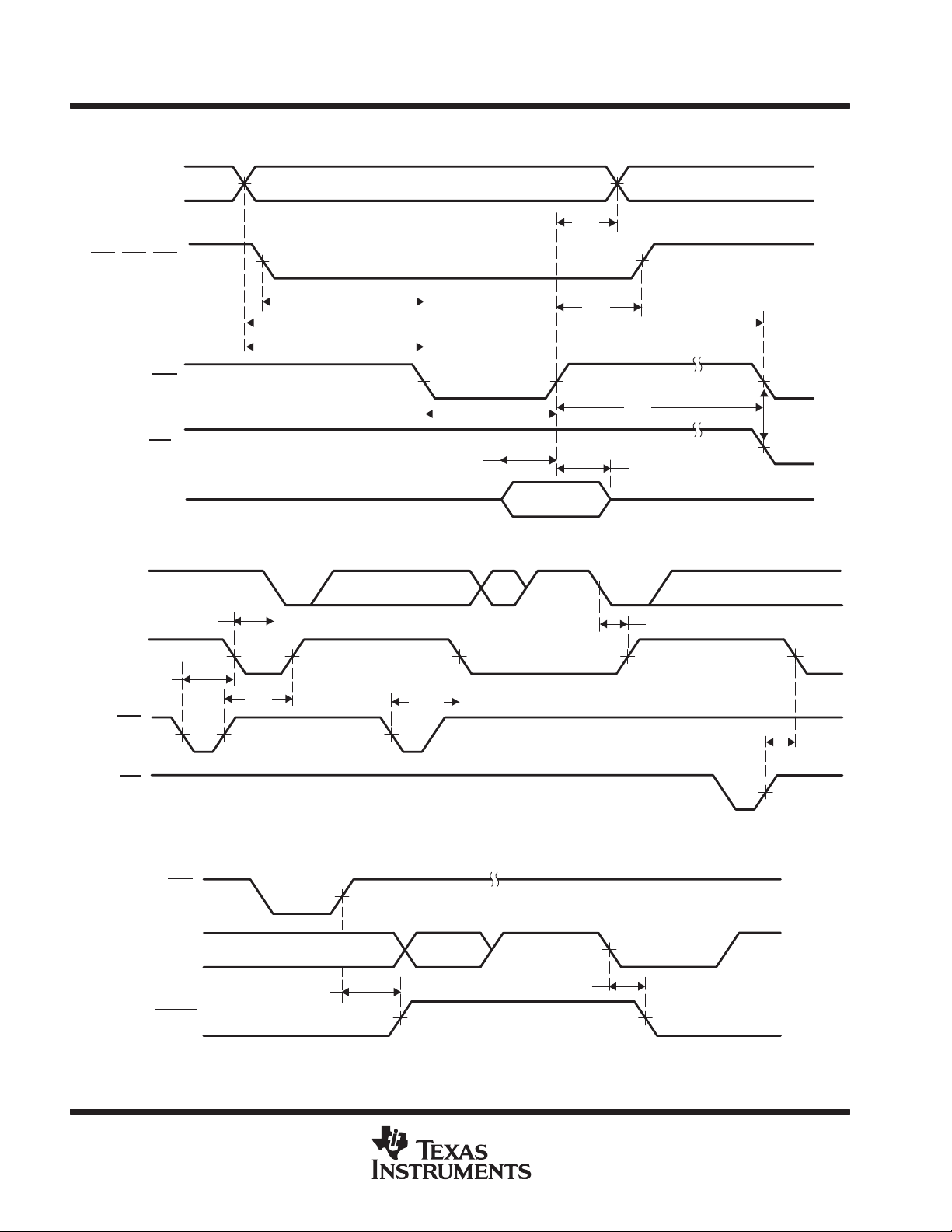
Figure 6. Transmitter Timing Waveforms
Byte #1
50%
t
ParityData Stop
pd5
50%
50%
t
d8
50%
Figure 7. Transmitter Ready Mode 0 Timing Waveforms
POST OFFICE BOX 655303 • DALLAS, TEXAS 75265
50%
Start

TL16C552A, TL16C552AM
DUAL ASYNCHRONOUS COMMUNICATIONS ELEMENT
SLLS189D – NOVEMBER 1994 – REVISED JANUARY 1999
PARAMETER MEASUREMENT INFORMATION
WITH FIFO
IOW
(WR THR)
SOUT
TXRDY
RCLK
CLK
TL16C450 Mode
SIN
(receiver input
data)
Sample
CLK
Interrupt
(data ready or
RCVR ERR)
Byte #16
t
pd5
50%
ParityData Stop
50% 50%
Start
FIFO Full
Figure 8. Transmitter Ready Mode 1 Timing Waveforms
Start
8 CLK Cycles
ParityData Bits 5–8
t
d9
Stop
t
pd6
50%
t
pd7
Start of
Byte #16
t
d8
50%
IOR
50%
Figure 9. Receiver Timing Waveforms
Active
POST OFFICE BOX 655303 • DALLAS, TEXAS 75265
13

TL16C552A, TL16C552AM
DUAL ASYNCHRONOUS COMMUNICATIONS ELEMENT
WITH FIFO
SLLS189D – NOVEMBER 1994 – REVISED JANUARY 1999
PARAMETER MEASUREMENT INFORMATION
SIN
Sample
CLK
Trigger
Interrupt
(FCR6, 7=0, 0)
IOR
(RD RBR)
LSI
Interrupt
IOR
(RD LSR)
SIN
Sample
CLK
Start
ParityData Bits 5–8
Stop
50%
t
d9
50%
50%
t
Active
50%
pd7
Figure 10. Receiver FIFO First Byte (Sets RDR) Waveforms
Stop
t
pd7
50%
50%
(FIFO at or above
trigger level)
(FIFO below
trigger level)
Active
t
Time Out or
Trigger Level
Interrupt
LSI
Interrupt
IOR
(RD LSR)
IOR
(RD RBR)
NOTE A: This is the reading of the last byte in the FIFO.
(see Note A)
Previous Byte
Read From FIFO
d9
50%
t
d9
50% 50%
Figure 11. Receiver FIFO After First Byte (After RDR Set) Waveforms
50%
Top Byte of FIFO
t
pd7
Active
50%
50%
50%
(FIFO at or above
trigger level)
(FIFO below
t
pd7
ActiveActive
trigger level)
14
POST OFFICE BOX 655303 • DALLAS, TEXAS 75265

TL16C552A, TL16C552AM
DUAL ASYNCHRONOUS COMMUNICATIONS ELEMENT
SLLS189D – NOVEMBER 1994 – REVISED JANUARY 1999
PARAMETER MEASUREMENT INFORMATION
WITH FIFO
IOR
(RD RBR)
SIN
(first byte)
Sample
CLK
RXRDY
NOTES: A. This is the reading of the last byte in the FIFO.
B. If FCR0 = 1, td9 = 3 RCLK cycles. For a time-out interrupt, td9 = 8 RCLK cycles.
(see Note B )
Stop
t
d9
50%
Figure 12. Receiver Ready Mode 0 Waveforms
IOR
(RD RBR)
(first byte that reaches
the trigger level)
SIN
Stop
Sample
CLK
t
pd8
50%
Active
(see Note A)
50%
(see Note A)
50%
Active
t
(see Note B)
RXRDY
NOTES: A. This is the reading of the last byte in the FIFO.
B. If FCR0–1, td9 = 3 RCLK cycles. For a trigger change level interrupt, td9 = 8 RCLK.
d9
Figure 13. Receiver Ready Mode 1 Waveforms
50%
t
50%
pd8
POST OFFICE BOX 655303 • DALLAS, TEXAS 75265
15

TL16C552A, TL16C552AM
DUAL ASYNCHRONOUS COMMUNICATIONS ELEMENT
WITH FIFO
SLLS189D – NOVEMBER 1994 – REVISED JANUARY 1999
PARAMETER MEASUREMENT INFORMATION
IOW
(WR MCR)
, DTR
RTS
CTS, DSR, DCD
INT0, INT1,
1 INT, 2 INT
IOR
(RD MSR)
RI
DATA
50% 50%
t
pd9
50%50%
t
pd10
50% 50% 50% 50%
t
pd11
50%
t
pd10
Figure 14. Modem Control Timing Waveforms
t
su7
50%
Valid
50%
t
h6
50%50%
t
pd12
50%
t
pd9
STB
ACK
BUSY
50% 50%
t
w6
t
d10
50% 50% 50%
t
d12
t
w7
Figure 15. Parallel Port Timing Waveforms
t
d11
50%50%
t
w8
16
POST OFFICE BOX 655303 • DALLAS, TEXAS 75265

DUAL ASYNCHRONOUS COMMUNICATIONS ELEMENT
SLLS189D – NOVEMBER 1994 – REVISED JANUARY 1999
PARAMETER MEASUREMENT INFORMATION
ENIRQ
TL16C552A, TL16C552AM
WITH FIFO
ACK
INT2
Line Printer
Status Register,
Bit 2 (PRINT
(RD_LPS)
NOTE A: A timing value is not provided for t
)
IOR
Figure 16. Parallel Port AT Mode Timing (ENIRQ = Low) Waveforms
ENIRQ
ACK
INT2
50%
50%
t
d14
50%50%
50%
50%
t
d13
in the tables because the line printer status register, bit 2 (PRINT
d(int)
50%
t
d15
t
50%
d16
t
d(int
(see Note A)
50%
) is an internal signal.
PRINT
IOR
(RD_LPS)
50%
Figure 17. Parallel Port PS/2 Mode Timing (ENIRQ = High) Waveforms
RESET
50%50%
t
w3
Figure 18. RESET Voltage Waveform
POST OFFICE BOX 655303 • DALLAS, TEXAS 75265
17

TL16C552A, TL16C552AM
DUAL ASYNCHRONOUS COMMUNICATIONS ELEMENT
WITH FIFO
SLLS189D – NOVEMBER 1994 – REVISED JANUARY 1999
PRINCIPLES OF OPERATION
Three types of information are stored in the internal registers used in the ACE: control, status, and data. Mnemonic
abbreviations for the internal registers are shown in Table 1.
Table 1. Internal Register Mnemonic Abbreviations
CONTROL MNEMONIC STATUS MNEMONIC DATA MNEMONIC
Line control register LCR Line status register LSR Receiver buffer register RBR
FIFO control register FCR Modem status register MSR Transmitter holding register THR
Modem control register MCR
Divisor latch LSB DLL
Divisor latch MSB DLM
Interrupt enable register IER
The address, read, and write inputs are used with the divisor latch access bit (DLAB) in the line control register (bit 7)
to select the register to be written to or read from (see Table 2). Individual bits within the registers are referred to by
the register mnemonic and the bit number in parenthesis. As an example, LCR7 refers to line control register bit 7.
The transmitter holding register and receiver buffer register are data registers that hold from five to eight bits of data.
If fewer than eight data bits are transmitted, data is right justified to the LSB. Bit 0 of a data word is always the first
serial data bit received and transmitted. The ACE data registers are double buffered (TL16C450 mode) or FIFO
buffered (FIFO mode) so that read and write operations can be performed when the ACE is performing the
parallel-to-serial or serial-to-parallel conversion.
Table 2. Register Selection
DLAB A2 A1 A0 MNEMONIC REGISTER
L L L L RBR Receiver buffer register (read only)
L L L L THR Transmitter holding register (write only)
L L L H IER Interrupt enable register
X L H L IIR Interrupt identification register (read only)
X L H L FCR FIFO control register (write only)
X L H H LCR Line control register
X H L L MCR Modem control register
X H L H LSR Line status register
X H H L MSR Modem status register
X H H H SCR Scratch pad register
H L L L DLL LSB divisor latch
H L L H DLM MSB divisor latch
†
The serial channel is accessed when either CS0
X = irrelevant, L = low level, H = high level
or CS1 is low.
†
18
POST OFFICE BOX 655303 • DALLAS, TEXAS 75265

TL16C552A, TL16C552AM
ADDRESS
(
)
(
)
(
)
1
IER0000
(EDSSI) Enable
(ERLSI)
(ETBEI)
(ERBFI)
modem status
Enable
Enable
Enable
g
g
2
FCR
Receiver
Receiver
Reserved
Reserved
DMA
Transmitter
Receiver
FIFO
(writ
)
tri
(MSB)
tri
(LSB)
t
FIFO
t
FIFO
t
()
()
()
()
()
()
()
()
(INT
INT1)
l)
()
()
()
()
()
()
()
‡
empty
6
MSR
(DCD)
(RI)
(DSR)
(CTS)
(∆DCD)
(TERI)
(∆DSR)
(∆CTS)
Data carrier
Ring
Data set
Clear
Delta data
Trailing edge
Delta data
Delta clear
detect
indicator
ready
to send
carrier detect
ring indicator
set ready
clear to send
DUAL ASYNCHRONOUS COMMUNICATIONS ELEMENT
WITH FIFO
SLLS189D – NOVEMBER 1994 – REVISED JANUARY 1999
PRINCIPLES OF OPERATION
accessible registers
Using the CPU, the system programmer has access to and control over any of the ACE registers that are
summarized in Table 1. These registers control ACE operations, receive data, and transmit data. Descriptions
of these registers follow Table 3.
Table 3. Summary of Accessible Registers
REGISTER
MNEMONIC
0 RBR
0 THR Data Data Data Data Data Data Data Data
†
0
†
1
1 IER 0 0 0 0
(read only)
(write only) Bit 7 Bit 6 Bit 5 Bit 4 Bit 3 Bit 2 Bit 1 Bit 0
DLL Bit 7 Bit 6 Bit 5 Bit 4 Bit 3 Bit 2 Bit 1 Bit 0
DLM Bit 15 Bit 14 Bit 13 Bit 12 Bit 11 Bit 10 Bit 9 Bit 8
BIT 7 BIT 6 BIT 5 BIT 4 BIT 3 BIT 2 BIT 1 BIT 0
Data Bit 7
(MSB)
Data Bit 6 Data Bit 5 Data Bit 4 Data Bit 3 Data Bit 2 Data Bit 1 Data Bit 0
REGISTER BIT NUMBER
EDSSI) Enable (ERLSI
modem status
interrupt
Enable
receiver line
status holding data
interrupt
ETBEI
Enable
transmitter
register available
empty interrupt
interrupt
(LSB)
ERBFI
Enable
received
e only
2 IIR FIFOs
3 LCR (DLAB) Set Stick (EPS) (PEN) (STB) (WLSB1) (WLSB0)
4 MCR 0 0 0 Loop OUT2 Enable OUT1 (RTS) (DTR)
5 LSR Error in (TEMT) (THRE) (BI) (FE) (PE) (OE) (DR)
7 SCR Bit 7 Bit 6 Bit 5 Bit 4 Bit 3 Bit 2 Bit 1 Bit 0
†
DLAB = 1
‡
These bits are always 0 when FIFOs are disabled.
(read only) enabled
gger
Divisor latch break parity
access bit select stop bits select bit 1 select bit 0
receiver
FIFO
‡
gger
FIFOs
‡
enabled
Transmitter
empty holding
Transmitter
mode selec
0 0 Interrupt ID
Even parity
Break
interrupt error error error ready
register
p
Parity enable
external (an unused
interrupt
Framing
bit 3
0 or
rese
‡
Interrupt ID Interrupt ID 0 if
bit 2 bit 1 interrupt
Number of
internal
signa
Parity
rese
Word length
Request
to send terminal
Overrun
enable
pending
Word length
Data
ready
Data
POST OFFICE BOX 655303 • DALLAS, TEXAS 75265
19

TL16C552A, TL16C552AM
DUAL ASYNCHRONOUS COMMUNICATIONS ELEMENT
WITH FIFO
SLLS189D – NOVEMBER 1994 – REVISED JANUARY 1999
PRINCIPLES OF OPERATION
FIFO control register (FCR)
This write-only register is at the same location as the interrupt identification register. It enables and clears the
FIFOs, sets the trigger level of the receiver FIFO, and selects the type of DMA signaling.
D
Bit 0: FCR0 enables both the transmitter and receiver FIFOs. All bytes in both FIFOs can be cleared by
clearing FCR0. Data is cleared automatically from the FIFOs when changing from the FIFO mode to the
TL16C450 mode and vice versa. Programming of other FCR bits is enabled by setting FCR0.
D
Bit 1: When set, FCR1 clears all bytes in the receiver FIFO and resets the counter . This does not clear the
shift register.
D
Bit 2: When set, FCR2 clears all bytes in the transmitter FIFO and resets the counter . This does not clear
the shift register.
D
Bit 3: When set, FCR3 changes the RXRDY and TXRDY terminals from mode 0 to mode 1 when FCR0
is set.
D
Bits 4 and 5: FCR4 and FCR5 are reserved for future use.
D
Bits 6 and 7: FCR6 and FCR7 set the trigger level for the receiver FIFO interrupt (see Table 4).
Table 4. Receiver FIFO Trigger Level
BIT
7 6
0 0 01
0 1 04
1 0 08
1 1 14
RECEIVER FIFO
TRIGGER LEVEL (BYTES)
FIFO interrupt mode operation
The following receiver status occurs when the receiver FIFO and receiver interrupts are enabled:
1. LSR0 is set when a character is transferred from the shift register to the receiver FIFO. When the FIFO is
empty, it is reset.
2. IIR = 06 receiver line status interrupt has higher priority than the received data available interrupt
IIR = 04.
3. Receive data available interrupt is issued to the CPU when the programmed trigger level is reached by
the FIFO. When the FIFO drops below its programmed trigger level, it is cleared.
4. IIR = 04 (receive data available indicator) also occurs when the FIFO reaches its trigger level. It is
cleared when the FIFO drops below the programmed trigger level.
The following receiver FIFO character time-out status occurs when receiver FIFO and receiver interrupts are
enabled.
20
POST OFFICE BOX 655303 • DALLAS, TEXAS 75265

TL16C552A, TL16C552AM
DUAL ASYNCHRONOUS COMMUNICATIONS ELEMENT
WITH FIFO
SLLS189D – NOVEMBER 1994 – REVISED JANUARY 1999
PRINCIPLES OF OPERATION
FIFO interrupt mode operation (continued)
1. When the following conditions exist, a FIFO character time-out interrupt occurs:
a. Minimum of one character in FIFO
b. The last received serial character is longer than four previous continuous-character times (if two stop
bits are programmed, the second one is included in the time delay).
c. The last CPU read of the FIFO is more than four previous continuous-character times. At 300 baud and
12-bit characters, the FIFO time-out interrupt causes a latency of 160 ms maximum from received
character to interrupt issued.1
2. By using the RCLK input for a clock signal, the character times can be calculated. The delay is proportional
to the baud rate.
3. The time-out timer is reset after the CPU reads the receiver FIFO or after a new character is received when
there has been no time-out interrupt.
4. A time-out interrupt is cleared and the timer is reset when the CPU reads a character from the receiver FIFO.
Transmitter interrupts occur as follows when the transmitter and transmitter FIFO interrupts are enabled
(FCR0 = 1, IER = 1).
1. When the transmitter FIFO is empty, the transmitter holding register interrupt (IIR = 02) occurs. The interrupt
is cleared when the transmitter holding register is written to or the IIR is read. One to sixteen characters can
be written to the transmit FIFO when servicing this interrupt.
2. The transmitter FIFO empty indicators are delayed one character time minus the last stop bit time when the
following occurs:
THRE = 1 and there is not a minimum of two bytes at the same time in transmitter FIFO since the last
THRE = 1. The first transmitter interrupt after changing FCR0 is immediate, assuming it is enabled.
Receiver FIFO trigger level and character time-out interrupts have the same priority as the received data
available interrupt. The transmitter holding register empty interrupt has the same priority as the transmitter FIFO
empty interrupt.
FIFO polled mode operation
Clearing IER0, IER1, IER2, IER3, or all with FCR0 = 1 puts the ACE into the FIFO polled mode. The receiver
and transmitter are controlled separately. Either one or both can be in the polled mode.
In the FIFO polled mode, there is no time-out condition indicated or trigger level reached. However, the receiver
and transmitter FIFOs still have the capability of holding characters. The LSR must be read to determine the
ACE status.
interrupt enable register (IER)
The IER independently enables the four serial channel interrupt sources that activate the interrupt (INT0 or
INT1) output. All interrupts are disabled by clearing IER0 – IER3. Interrupts are enabled by setting the
appropriate bits of the IER. Disabling the interrupt system inhibits the interrupt identification register and the
active (high) interrupt output. All other system functions operate in their normal manner, including the setting
of the LSRs and MSRs. The contents of the IER shown in Table 3 are described in the following bulleted list.
D
Bit 0: When IER0 is set, IER0 enables the received data available interrupt and the time-out interrupts in
the FIFO mode.
POST OFFICE BOX 655303 • DALLAS, TEXAS 75265
21

TL16C552A, TL16C552AM
DUAL ASYNCHRONOUS COMMUNICATIONS ELEMENT
WITH FIFO
SLLS189D – NOVEMBER 1994 – REVISED JANUARY 1999
PRINCIPLES OF OPERATION
interrupt enable register (IER) (continued)
D
Bit 1: When IER1 is set, the transmitter holding register empty interrupt is enabled.
D
Bit 2: When IER2 is set, the receiver line status interrupt is enabled.
D
Bit 3: When IER3 is set, the modem status interrupt is enabled.
D
Bits 4 – 7: IER4 through IER7 are cleared.
In order to minimize software overhead during data character transfers, the serial channel prioritizes interrupts
into four levels. The four levels of interrupt conditions are as follows:
D
Priority 1–Receiver line status (highest priority)
D
Priority 2–Receiver data ready or receiver character time out
D
Priority 3–Transmitter holding register empty
D
Priority 4–Modem status (lowest priority)
Information indicating that a prioritized interrupt is pending and the type of interrupt is stored in the IIR. The IIR
indicates the highest priority interrupt pending. The contents of the IIR are indicated in Table 5.
Table 5. Interrupt Control Functions
INTERRUPT
IDENTIFICATION
REGISTER
BIT 3 BIT 2 BIT 1 BIT 0
0 0 0 1 None None None None
0 1 1 0 First Receiver line status OE, PE, FE, or BI LSR read
0 1 0 0 Second Received data available Receiver data available or trigger level
1 1 0 0 Second Character time-out
0 0 1 0 Third THRE THRE IIR read if THRE is
0 0 0 0 Fourth Modem status CTS, DSR, RI, or DCD MSR read
D
Bit 0: IIR0 indicates whether an interrupt is pending. When IIR0 is cleared, an interrupt is pending.
D
Bits 1 and 2: IIR1 and IIR2 identify the highest priority interrupt pending, as indicated in Table 5.
D
Bit 3: IIR3 is always cleared in TL16C450 mode. This bit is set along with bit 2 in FIFO mode and when a
PRIORITY
LEVEL
INTERRUPT TYPE INTERRUPT SOURCE
indicator
INTERRUPT SET AND RESET FUNCTIONS
reached
No characters have been removed from or
input to the receiver FIFO during the last
four character times and there is at least
one character in it during this time.
INTERRUPT RESET
CONTROL
RBR read until FIFO
drops below the
trigger level
RBR read
the interrupt source
or THR write
trigger change level interrupt is pending.
22
D
Bits 4 and 5: IIR4 and IIR5 are always cleared.
D
Bits 6 and 7: IIR6 and IIR7 are set when FCR0 = 1.
POST OFFICE BOX 655303 • DALLAS, TEXAS 75265

TL16C552A, TL16C552AM
DUAL ASYNCHRONOUS COMMUNICATIONS ELEMENT
WITH FIFO
SLLS189D – NOVEMBER 1994 – REVISED JANUARY 1999
PRINCIPLES OF OPERATION
line control register (LCR)
The format of the data character is controlled by the LCR. The LCR can be read. Its contents are described in
the following bulleted list and shown in Figure 19.
D
Bits 0 and 1: LCR0 and LCR1 are the word length select bits. The number of bits in each serial character
is programmed as shown.
D
Bit 2: LCR2 is the stop bit select bit. LCR2 specifies the number of stop bits in each transmitted character .
The receiver always checks for one stop bit.
D
Bit 3: LCR3 is the parity enable bit. When LCR3 is set, a parity bit between the last data word bit and stop
bit is generated and checked.
D
Bit 4: LCR4 is the even parity select bit. When LCR4 is set, even parity is enabled.
D
Bit 5: LCR5 is the stick parity bit. When parity is enabled (LCR3 = 1), LCR5 = 1 causes the transmission
and reception of a parity bit to be in the opposite state from the value of LCR4. This forces parity to a known
state and allows the receiver to check the parity bit in a known state.
D
Bit 6: LCR6 is the break control bit. When LCR6 is set, the serial output (SOUT1/SOUT0) is forced to the
spacing state (low). The break control bit acts only on the serial output and does not affect the transmitter
logic. When the following sequence is used, no invalid characters are transmitted because of the break:
Step 1: Load a zero byte in response to the transmitter holding register empty (THRE) status indicator.
Step 2: Set the break in response to the next THRE status indicator.
Step 3: Wait for the transmitter to be idle when transmitter empty status signal is set high (TEMT = 1); then
clear the break when the normal transmission has to be restored.
D
Bit 7: LCR7 is the divisor latch access bit (DLAB) bit. LCR7 must be set to access the divisor latches DLL
and DLM of the baud rate generator during a read or write operation. LCR7 must be cleared to access the
receiver buffer register, the transmitter holding register, or the interrupt enable register.
POST OFFICE BOX 655303 • DALLAS, TEXAS 75265
23

TL16C552A, TL16C552AM
DUAL ASYNCHRONOUS COMMUNICATIONS ELEMENT
WITH FIFO
SLLS189D – NOVEMBER 1994 – REVISED JANUARY 1999
PRINCIPLES OF OPERATION
line control register (LCR) (continued)
Line Control Register
LCR7LCR6LCR5LCR4LCR3LCR2LCR1LCR
0
Word Length
Select
Stop Bit
Select
0 0 = 5 Data Bits
0 1 = 6 Data Bits
1 0 = 7 Data Bits
1 1 = 8 Data Bits
0 = 1 Stop Bits
1 = 1.5 Stop Bits if 5 Data Bits Selected
2 Stop Bits if 6, 7, 8 Data Bits Selected
Parity Enable
Even Parity
Select
Stick Parity
Break Control
Divisor Latch
Access Bit
0 = Parity Disabled
1 = Parity Enabled
0 = Odd Parity
1 = Even Parity
0 = Stick Parity Disabled
1 = Stick Parity Enabled
0 = Break Disabled
1 = Break Enabled
0 = Access Receiver Buffer
1 = Access Divisor Latches
Figure 19. Line Control Register Contents
line printer port
The line printer port contains the functionality of the port included in the TL16C452 but offers a hardware
programmable extended mode controlled by the printer enhancement mode (PE) terminal. This enhancement
is the addition of a direction control bit and an interrupt status bit.
register 0 line printer data register
The line printer (LPT) port is either output only or bidirectional depending on the state of the extended mode
terminal and data direction control bits.
Compatibility mode (PEMD = L)
Reads to the LPT data register and returns the last data that was written to the port. Write operations
immediately output data to PD0–PD7.
Extended mode (PEMD = H)
Read operations return either the data last written to the LPT data register when the direction bit is cleared or
return the data that is present on PD0 – PD7 when the direction is set to read. Write operations to the LPT
data register latch data into the output register; however, they only drive the LPT port when the direction bit is
cleared.
24
POST OFFICE BOX 655303 • DALLAS, TEXAS 75265

TL16C552A, TL16C552AM
DUAL ASYNCHRONOUS COMMUNICATIONS ELEMENT
WITH FIFO
SLLS189D – NOVEMBER 1994 – REVISED JANUARY 1999
PRINCIPLES OF OPERATION
line printer port (continued)
Table 6 summarizes the configuration of the PD port based on the combinations of the logic level on the
PEMD terminal and the value of the direction control bit (DIR).
Table 6. Extended Mode and Direction Control Bit Combinations
PEMD DIR PD0–PD7 FUNCTION
L X PC/AT mode – output
H 0 PS/2 mode – output
H 1 PS/2 mode – input
register 1 read line printer status register
The line printer status (LPS) register is a read-only register that contains interrupt and printer status of the LPT
connector terminals. Table 7 (in the default column) shows the values of each bit after reset in the case of the
printer being disconnected from the port.
Table 7. LPS Register Bit Description
BIT DESCRIPTION DEF AULT
0 Reserved 1
1 Reserved 1
2 PRINT 1
3 ERR †
4 SLCT †
5 PE †
6 ACK †
7 BSY †
†
Outputs are dependent upon device inputs.
D
Bits 0 and 1: LPS0 and LPS1 are reserved and always set.
D
Bit 2: LPS2 is the printer interrupt (PRINT, active low) status bit. When cleared, LPS2 indicates that the
printer has acknowledged the previous transfer with an ACK handshake (if bit 4 of the control register is set).
The bit is cleared on the active-to-inactive transition of the ACK
signal. This bit is set after a read of the status
port.
D
Bit 3: ERR is the error status bit and corresponds to ERR input.
D
Bit 4: SLCT is the select status bit and corresponds to SLCT input.
D
Bit 5: PE is the paper empty status bit and corresponds to PE input.
D
Bit 6: ACK is the acknowledge status bit corresponds to ACK input.
D
Bit 7: BSY is the busy status bit and corresponds to BUSY input (active high).
POST OFFICE BOX 655303 • DALLAS, TEXAS 75265
25

TL16C552A, TL16C552AM
DUAL ASYNCHRONOUS COMMUNICATIONS ELEMENT
WITH FIFO
SLLS189D – NOVEMBER 1994 – REVISED JANUARY 1999
PRINCIPLES OF OPERATION
register 2 line printer control register
The line printer control (LPC) register is a read/write port that controls the PD0–PD7 direction and drives the
printer control lines. Write operations set or clear these bits, whereas read operations return the state of the last
write operation to this register. The bits in this register are defined in Table 8 and the following bulleted list.
Table 8. LPC Register Bit Description
BIT DESCRIPTION
0 STB
1 AFD
2 INIT
3 SLIN
4 INT2 EN
5 DIR
6 Reserved 0
7 Reserved 0
D
Bit 0: STB is the printer strobe control bit. When STB is set, the STB signal is asserted on the LPT interface.
When STB is cleared, the STB
D
Bit 1: AFD is the autofeed control bit. When AFD is set, the AFD signal is asserted on the LPT interface.
When AFD is cleared, the signal is negated.
D
Bit 2: INIT is the initialize printer control bit. When INIT is set, the INIT signal is negated. When INIT is
cleared, the INIT
D
Bit 3: SLIN is the select input control bit. When SLIN is set, the SLIN signal is asserted on the LPT interface.
When SLIN is cleared, the signal is negated.
D
Bit 4: INT2 EN is the interrupt request enable control bit. When set, INT2 EN enables interrupts from the
LPT port. When cleared, INT2 EN disables interrupts and places INT2 signal in the high-impedance state.
D
Bit 5: DIR is the direction control bit which is only used when PEMD is high. When DIR is set, the output
buffers in the LPD port are disableded to allow data driven from external sources to be read from the LPD
port. When DIR is cleared, the LPD port is in the output mode.
D
Bits 6 and 7: These bits are reserved and are always cleared.
signal is asserted on the LPT interface.
signal is negated.
26
POST OFFICE BOX 655303 • DALLAS, TEXAS 75265

TL16C552A, TL16C552AM
DUAL ASYNCHRONOUS COMMUNICATIONS ELEMENT
WITH FIFO
SLLS189D – NOVEMBER 1994 – REVISED JANUARY 1999
PRINCIPLES OF OPERATION
line status register (LSR)
The LSR is a single register that provides status indicators. The LSR bits shown in T able 9 are described in the
following bulleted list.
D
Bit 0: DR is the data ready bit. When set, an incoming character is received and transferred into the receiver
buffer register or in the FIFO. LSR0 is cleared by a CPU read of the data in the receiver buffer register or
in the FIFO.
D
Bit 1: OE is the overrun error bit. An OE indicates that data in the receiver buffer register is not read by the
CPU before the next character is transferred into the receiver buffer register overwriting the previous
character. The OE indicator is cleared whenever the CPU reads the contents of the LSR. An overrun error
occurs in FIFO mode after the FIFO is full and the next character is completely received. The overrun error
is detected by the CPU on the first LSR read after it happens. The character in the shift register is not
transferred to the FIFO, but it is overwritten.
D
Bit 2: PE is the parity error bit. A PE indicates that the received data character does not have the correct
parity as selected by LCR3 and LCR4. The PE bit is set upon detection of a parity error and is cleared when
the CPU reads the contents of the LSR. In FIFO mode, the parity error is associated with a particular
character in the FIFO. LSR2 reflects the error when the character is at the top of the FIFO.
D
Bit 3: FE is the framing error bit. An FE indicates that the received character does not have a valid stop bit.
LSR3 is set when the stop bit following the last data bit or parity bit is detected as a zero bit (spacing level).
The FE indicator is cleared when the CPU reads the contents of the LSR. In FIFO mode, the framing error
is associated with a particular character in the FIFO. LSR3 reflects the error when the character is at the
top of the FIFO.
D
Bit 4: BI is the break interrupt bit. BI is set when the received data input is held in the spacing (low) state
for longer than a full word transmission time (start bit + data bits + parity + stop bits). The BI indicator is
cleared when the CPU reads the contents of the LSR. In FIFO mode, this is associated with a particular
character in the FIFO. LSR4 reflects BI when the break character is at the top of the FIFO. The error is
detected by the CPU when its associated character is at the top of the FIFO during the first LSR read. Only
one zero character is loaded into the FIFO when BI occurs.
LSR1 – LSR4 are the error conditions that produce a receiver line status interrupt (priority 1 interrupt in the
interrupt identification register) when any of the conditions are detected. This interrupt is enabled by setting IER2
in the interrupt enable register.
D
Bit 5: THRE is the transmitter holding register empty bit. THRE indicates that the ACE is ready to accept
a new character for transmission. The THRE bit is set when a character is transferred from the transmitter
holding register into the transmitter shift register. LSR5 is cleared by the loading of the transmitter holding
register by the CPU. LSR5 is not cleared by a CPU read of the LSR. In FIFO mode when the transmitter
FIFO is empty , this bit is set. It is cleared when one byte is written to the transmitter FIFO. When the THRE
interrupt is enabled by IER1, THRE causes a priority 3 interrupt in the IIR. If THRE is the interrupt source
indicated in IIR, INTRPT is cleared by a read of the IIR.
D
Bit 6: TEMT is the transmitter empty bit. TEMT is set when the transmitter holding register (THR) and the
transmitter shift register are both empty. LSR6 is cleared when a character is loaded into the THR and
remains cleared until the character is transferred out of SOUT. TEMT is not cleared by a CPU read of the
LSR. In FIFO mode, when both the transmitter FIFO and shift register are empty, TEMT is set.
D
Bit 7: LSR7 is the receiver FIFO error bit. The LSR7 bit is always cleared in TL16C450 mode. In FIFO mode,
it is set when at least one of the following data errors occurs in the FIFO: parity error , framing error, or break
interrupt indicator. It is cleared when the CPU reads the LSR if there are no subsequent errors in the FIFO.
POST OFFICE BOX 655303 • DALLAS, TEXAS 75265
27

TL16C552A, TL16C552AM
DUAL ASYNCHRONOUS COMMUNICATIONS ELEMENT
WITH FIFO
SLLS189D – NOVEMBER 1994 – REVISED JANUARY 1999
PRINCIPLES OF OPERATION
line status register (LSR) (continued)
NOTE:
The LSR may be written to. However, this function is intended only for factory test. It should be
considered as read only by applications software.
Table 9. Line Status Register Bits
LSR BITS 1 0
LSR0 data ready (DR) Ready Not ready
LSR1 overrun error (OE) Error No error
LSR2 parity error (PE) Error No error
LSR3 framing error (FE) Error No error
LSR4 break interrupt (BI) Break No break
LSR5 transmitter holding register empty (THRE) Empty Not empty
LSR6 transmitter empty (TEMT) Empty Not empty
LSR7 receiver FIFO error Error in FIFO No error in FIFO
master reset
After power up, the ACE RESET input should be held low for one microsecond to reset the ACE circuits to an
idle mode until initialization. A low on RESET
D
It initializes the transmitter and receiver clock counters.
D
It clears the LSR except for transmitter shift register empty (TEMT) and transmit holding register empty
(THRE), which are set. The MCR is also cleared. All of the discrete lines, memory elements, and
miscellaneous logic associated with these register bits are also cleared or turned off. The LCR, divisor
latches, receiver buffer register, and transmitter holding buffer register are not affected.
Following the removal of the reset condition (RESET
A hardware reset of the ACE sets the THRE and TEMT status bit in the LSR. When interrupts are subsequently
enabled, an interrupt occurs due to THRE. A summary of the effect of a reset on the ACE is given in Table 10.
causes the following:
high), the ACE remains in idle mode until programmed.
28
POST OFFICE BOX 655303 • DALLAS, TEXAS 75265

TL16C552A, TL16C552AM
Interrupt identification register
Reset
, ,,,, , y
DUAL ASYNCHRONOUS COMMUNICATIONS ELEMENT
SLLS189D – NOVEMBER 1994 – REVISED JANUARY 1999
PRINCIPLES OF OPERATION
master reset (continued)
Table 10. RESET Effects on Registers and Signals
REGISTER/SIGNAL RESET CONTROL RESET
Interrupt enable register Reset All bits cleared (0–3 forced and 4–7 permanent)
p
Line control register Reset All bits are cleared.
Modem control register Reset All bits are cleared (5–7 permanently).
FIFO control register Reset All bits are cleared.
Line status register Reset All bits are cleared, except bits 5 and 6 are set.
Modem status register Reset Bits 0–3 are cleared, bits 4–7 input signal.
SOUT Reset High
Interrupt (RCVR errors) Read LSR/Reset Low
Interrupt (receiver data ready) Read RBR/Reset Low
Interrupt (THRE) Read IIR/W rite THR/Reset Low
Interrupt (modem status changes) Read MSR/Reset Low
OUT2 Reset High
RTS Reset High
DTR Reset High
OUT1 Reset High
Bit 0 is set, bits 1, 2, 3, 6, and 7 are cleared, and bits 4–5 are permanently
cleared.
WITH FIFO
modem control register (MCR)
The MCR controls the interface with the modem or data set as described in Figure 20. MCR can be written to
and read from. The RTS
asserts a low signal (active) at the output terminals. The MCR bits are defined in the following bulleted list.
D
Bit 0: When MCR0 is set, the DTR output is forced low . When MCR0 is cleared, the DTR output is forced
high. The DTR
proper polarity input at the modem or data set.
D
Bit 1: When MCR1 is set, the RTS output is forced low. When MCR1 is cleared, the RTS output is forced
high. The RTS
polarity input at the modem or data set.
D
Bit 2: MCR2 has no effect on operation.
D
Bit 3: When MCR3 is set, the external serial channel interrupt is enabled.
D
Bit 4: MCR4 provides a local loopback feature for diagnostic testing of the channel. When MCR4 is set,
SOUT is set to the marking (high) state and the SIN is disconnected. The output of the transmitter shift
register is looped back into the receiver shift register input. The four modem control inputs (CTS
and RI
) are disconnected. The modem control outputs (DTR, RTS, OUT1, and OUT2) are internally
connected to the four modem control inputs. The modem control output terminals are forced to their inactive
(high) state on the TL16C552A. In the diagnostic mode, data transmitted is immediately received. This
allows the processor to verify the transmit and receive data paths of the selected serial channel. Interrupt
control is fully operational; however, interrupts are generated by controlling the lower four MCR bits
internally . Interrupts are not generated by activity on the external terminals represented by those four bits.
and DTR outputs are directly controlled by their control bits in this register. A high input
output of the serial channel can be input into an inverting line driver in order to obtain the
output of the serial channel can be input into an inverting line driver to obtain the proper
, DSR, DCD,
POST OFFICE BOX 655303 • DALLAS, TEXAS 75265
29

TL16C552A, TL16C552AM
DUAL ASYNCHRONOUS COMMUNICATIONS ELEMENT
WITH FIFO
SLLS189D – NOVEMBER 1994 – REVISED JANUARY 1999
PRINCIPLES OF OPERATION
modem control register (MCR) (continued)
D
Bits 5 – 7: MCR5 – MCR7 are permanently cleared.
Modem Control Register
MCR7MCR6MCR5MCR4MCR3MCR2MCR1MCR
0
Data Terminal
Ready
Request
to Send
Out 1
(internal)
Out 2
(internal)
Loop
Bits Are Cleared
0 = DTR Output High (inactive)
Output Low (active)
1 = DTR
0 = RTS
Output High (inactive)
Output Low (active)
1 = RTS
No Effect on External Operation
0 = External Interrupt Disabled
1 = External Interrupt Enabled
0 = Loop Disabled
1 = Loop Enabled
Figure 20. Modem Control Register Contents
modem status register (MSR)
The MSR provides the CPU with status of the modem input lines from the modem or peripheral devices. The
MSR allows the CPU to read the serial channel modem signal inputs. This is done by accessing the data bus
interface of the ACE in addition to the current status of four bits of the MSR. These four bits indicate whether
the modem inputs have changed since the last reading of the MSR. The delta status bits are set when a control
input from the modem changes state and are cleared when the CPU reads the MSR.
The modem input lines are CTS
, DSR, RI, and DCD. MSR4 – MSR7 are status indicators of these lines. A set
status bit indicates that the input is low. A cleared status bit indicates that the input is high. When the modem
status interrupt in the interrupt enable register is enabled (IER3), an interrupt is generated whenever MSR0 –
MSR3 is set. The MSR is a priority-4 interrupt. The contents of the MSR are described in Table 11.
D
Bit 0: MSR0 is the delta clear-to-send (∆CTS) bit. ∆CTS displays that the CTS input to the serial channel
has changed states since it was last read by the CPU.
D
Bit 1: MSR1 is the delta data set ready (∆DSR) bit. ∆DSR indicates that the DSR input to the serial channel
has changed states since the last time it was read by the CPU.
D
Bit 2: MSR2 is the trailing edge of the ring indicator (TERI) bit. TERI indicates that the RI input to the serial
channel has changed states from low to high since the last time it was read by the CPU. High-to-low
transitions on RI do not activate TERI.
30
POST OFFICE BOX 655303 • DALLAS, TEXAS 75265

DUAL ASYNCHRONOUS COMMUNICATIONS ELEMENT
PRINCIPLES OF OPERATION
modem status register (MSR) (continued)
D
Bit 3: MSR3 is the delta data carrier detect (∆ DCD) bit. ∆DCD indicates that the DCD input to the serial
channel has changed states since the last time it was read by the CPU.
D
Bit 4: MSR4 is the clear-to-send (CTS) bit. CTS is the complement of the CTS input from the modem that
indicates to the serial channel that the modem is ready to receive data from SOUT . When the serial channel
is in the loop mode (MCR4 is set), MSR4 reflects the value of RTS in the MCR.
D
Bit 5: MSR5 is the data set ready (DSR) bit. DSR is the complement of the DSR input from the modem to
the serial channel that indicates that the modem is ready to provide received data to the serial channel
receiver circuitry . When the channel is in loop mode (MCR4 is set), MSR5 reflects the value of DTR in the
MCR.
D
Bit 6: MSR6 is the ring indicator (RI) bit. RI is the complement of the RI input. When the channel is in loop
mode (MCR4 is set), MSR6 reflects the value of OUT1
D
Bit 7: MSR7 is the data carrier detect (DCD) bit. Data carrier detect indicates the status of the data carrier
detect (DCD
the MCR.
) input. When the channel is in loop mode (MCR4 is set), MSR7 reflects the value of OUT2 in
TL16C552A, TL16C552AM
WITH FIFO
SLLS189D – NOVEMBER 1994 – REVISED JANUARY 1999
in the MCR.
Reading the MSR register clears the delta modem status indicators but has no effect on the other status bits.
For LSR and MSR, the setting of status bits is inhibited during status register read operations. If a status
condition is generated during a read IOR
operation, the status bit is not set until the trailing edge of the read.
When a status bit is set during a read operation and the same status condition occurs, that status bit is
cleared at the trailing edge of the read instead of being set again. In loop back mode, when modem status
interrupts are enabled, the CTS
, DSR, RI and DCD input terminals are ignored; however, a modem status
interrupt can still be generated by writing to MCR3–MCR0. Applications software should not write to the
MSR.
Table 11. Modem Status Register Bits
MSR BIT MNEMONIC DESCRIPTION
MSR0 ∆CTS Delta clear to send
MSR1 ∆DSR Delta data set ready
MSR2 TERI Trailing edge of ring indicator
MSR3 ∆DCD Delta data carrier detect
MSR4 CTS Clear to send
MSR5 DSR Data set ready
MSR6 RI Ring indicator
MSR7 DCD Data carrier detect
POST OFFICE BOX 655303 • DALLAS, TEXAS 75265
31

TL16C552A, TL16C552AM
REGISTER
REGISTER SELECTED
DUAL ASYNCHRONOUS COMMUNICATIONS ELEMENT
WITH FIFO
SLLS189D – NOVEMBER 1994 – REVISED JANUARY 1999
PRINCIPLES OF OPERATION
parallel port registers
The TL16C552A parallel port can connect the device to a Centronic-style printer interface. When chip select 2
) is low, the parallel port is selected. Table 12 shows the registers associated with this parallel port. The
(CS2
read or write function of the register is controlled by the state of the read (IOR
shown. The read data register allows the microprocessor to read the information on the parallel bus.
The read status register allows the microprocessor to read the status of the printer in the six most significant
bits. The status bits are printer busy BSY
selected (SLCT
), error (ERR), and printer interrupt (PRINT). The read control register allows the state of the
, acknowledge (ACK) (a handshake function), paper empty (PE), printer
control lines to be read. The write control register sets the state of the control lines. They are direction (DIR),
interrupt enable (INT2 EN), select in (SLIN), initialize the printer (INIT), autofeed the paper (AFD), and strobe
(STB
), which informs the printer of the presence of a valid byte on the parallel bus. The write data register allows
the microprocessor to write a byte to the parallel bus. The parallel port is completely compatible with the parallel
port implementation used in the IBM serial parallel adapter.
Table 12. Parallel Port Registers
REGISTER BITS
BIT 7 BIT 6 BIT 5 BIT 4 BIT 3 BIT 2 BIT 1 BIT 0
Read data PD7 PD6 PD5 PD4 PD3 PD2 PD1 PD0
Read status BSY ACK PE SLCT ERR PRINT 1 1
Read control 0 0 PEMD • DIR INT2 EN SLIN INIT AFD STB
Write data PD7 PD6 PD5 PD4 PD3 PD2 PD1 PD0
Write control 0 0 DIR INT2 EN SLIN INIT AFD STB
) and write (IOW) terminals as
Table 13. Parallel Port Register Select
CONTROL PINS
IOR IOW CS2 A1 A0
L H L L L Read data
L H L L H Read status
L H L H L Read control
L H L H H Invalid
H L L L L Write data
H L L L H Invalid
H L L H L Write control
H L L H H Invalid
programmable baud rate generator
The ACE serial channel contains a programmable baud rate generator (BRG) that divides the clock (dc to
8 MHz) by any divisor from 1 to (2
# = clock ÷ (baud rate x 16)], referred to in this document as RCLK. Two 8-bit divisor latch registers store the
divisor in a 16-bit binary format. These divisor latch registers must be loaded during initialization. Upon loading
either of the divisor latches, a 16-bit baud counter is immediately loaded. This prevents long counts on initial
load. The BRG can use any of three different popular frequencies to provide standard baud rates. These
frequencies are 1.8432 MHz, 3.072 MHz, and 8 MHz. With these frequencies, standard bit rates from 50 to
512 kbps are available. Tables 14, 15, 16, and 17 illustrate the divisors needed to obtain standard rates using
these three frequencies.
16
–1). The output frequency of the baud generator is 16x the data rate [divisor
32
POST OFFICE BOX 655303 • DALLAS, TEXAS 75265

DUAL ASYNCHRONOUS COMMUNICATIONS ELEMENT
PRINCIPLES OF OPERATION
programmable baud rate generator (continued)
Table 14. Baud Rates Using a 1.8432-MHz Crystal
TL16C552A, TL16C552AM
WITH FIFO
SLLS189D – NOVEMBER 1994 – REVISED JANUARY 1999
BAUD RATE
DESIRED
50
75
110
134.5
150
300
600
1200
1800
2000
2400
3600
4800
7200
9600
19200
38400
56000
BAUD RATE
DESIRED
50
75
110
134.5
150
300
600
1200
1800
2000
2400
3600
4800
7200
9600
19200
38400
DIVISOR (N) USED TO
GENERATE 16x CLOCK
2304
1536
1047
857
768
384
192
96
64
58
48
32
24
16
12
6
3
2
PERCENT ERROR DIFFERENCE
BETWEEN DESIRED AND ACTUAL
0.026
0.058
0.690
2.860
Table 15. Baud Rates Using a 3.072-MHz Crystal
DIVISOR (N) USED TO
GENERATE 16x CLOCK
3840
2560
1745
1428
1280
640
320
160
107
96
80
53
40
27
20
10
5
PERCENT ERROR DIFFERENCE
BETWEEN DESIRED AND ACTUAL
0.026
0.034
0.312
0.628
1.230
–
–
–
–
–
–
–
–
–
–
–
–
–
–
–
–
–
–
–
–
–
–
–
–
–
–
POST OFFICE BOX 655303 • DALLAS, TEXAS 75265
33

TL16C552A, TL16C552AM
DUAL ASYNCHRONOUS COMMUNICATIONS ELEMENT
WITH FIFO
SLLS189D – NOVEMBER 1994 – REVISED JANUARY 1999
PRINCIPLES OF OPERATION
programmable baud rate generator (continued)
Table 16. Baud Rates Using an 8-MHz Clock
BAUD RATE
DESIRED
50
75
110
134.5
150
300
600
1200
1800
2000
2400
3600
4800
7200
9600
19200
38400
56000
128000
256000
512000
BAUD RATE
DESIRED
50
75
110
134.5
150
300
600
1200
1800
2000
2400
3600
4800
7200
9600
19200
38400
56000
128000
256000
512000
1000000
DIVISOR (N) USED TO
GENERATE 16x CLOCK
10000
6667
4545
3717
3333
1667
833
417
277
250
208
139
104
69
52
26
13
9
4
2
1
PERCENT ERROR DIFFERENCE
BETWEEN DESIRED AND ACTUAL
Table 17. Baud Rates Using a 16-MHz Clock
DIVISOR (N) USED TO
GENERATE 16x CLOCK
20000
13334
9090
7434
6666
3334
1666
834
554
500
416
278
208
138
104
52
26
18
8
4
2
1
PERCENT ERROR DIFFERENCE
BETWEEN DESIRED AND ACTUAL
0.00
0.00
0.01
0.01
0.01
–0.02
0.04
–0.08
0.28
0.00
0.16
–0.08
0.16
0.64
0.16
0.16
0.16
–0.79
–2.34
–2.34
–2.34
0.00
–
0.005
0.010
0.013
0.010
0.020
0.040
0.080
0.080
–
0.160
0.080
0.160
0.644
0.160
0.160
0.160
0.790
2.344
2.344
2.400
34
POST OFFICE BOX 655303 • DALLAS, TEXAS 75265

TL16C552A, TL16C552AM
DUAL ASYNCHRONOUS COMMUNICATIONS ELEMENT
WITH FIFO
SLLS189D – NOVEMBER 1994 – REVISED JANUARY 1999
PRINCIPLES OF OPERATION
programming
The serial channel of the ACE is programmed by the control registers: LCR, IER, DLL, DLM, MCR, and FCR.
These control words define the character length, number of stop bits, parity , baud rate, and modem interface.
While the control registers can be written to in any order, the IER should be written to last because it controls
the interrupt enables. Once the serial channel is programmed and operational, these registers can be updated
any time the ACE serial channel is not transmitting or receiving data.
receiver
Serial asynchronous data is input into SIN. The ACE continually searches for a high-to-low transition
from the idle state. When the transition is detected, a counter is reset and counts the 16× clock to 7 1/2, which
is the center of the start bit. The start bit is valid if SIN is still low. Verifying the start bits prevents the receiver
from assembling a false data character due to a low-going noise spike on the SIN input.
The LCR determines the number of data bits in a character (LCR0 and LCR1). When parity is used, LCR3 and
the polarity of parity LCR4 is needed. Status for the receiver is provided in the LSR. When a full character is
received, including parity and stop bits, the data received indicator in LSR0 is set. The CPU reads the receiver
buffer register, which clears LSR0. If the character is not read prior to a new character transfer from the RSR
to the RBR, the overrun error status indicator is set in LSR1. If there is a parity error, the parity error is set in
LSR2. If a stop bit is not detected, a framing error indicator is set in LSR3.
If the data into SIN is a symmetrical square wave, the center of the data cells occurs within ±3.125% of the
actual center, providing an error margin of 46.875%. The start bit can begin as much as one 16× clock cycle
prior to being detected.
scratchpad register
The scratch register is an 8-bit read/write register that has no effect on either channel in the ACE. It is intended
to be used by the programmer to hold data temporarily.
POST OFFICE BOX 655303 • DALLAS, TEXAS 75265
35

TL16C552A, TL16C552AM
DUAL ASYNCHRONOUS COMMUNICATIONS ELEMENT
WITH FIFO
SLLS189D – NOVEMBER 1994 – REVISED JANUARY 1999
MECHANICAL DATA
HV (S-GQFP-F68) CERAMIC QUAD FLATPACK
61
1.500 (38,10)
1.300 (33,02)
60 44
1
9
SQ
43
27
0.025 (0,635)
0.013 (0,330)
0.008 (0,203)
0.400 (10,16) TYP
0.500 (12,70)
0.485 (12,32)
0.154 (3,912)
0.134 (3,404)
NOTES: A. All linear dimensions are in inches (millimeters).
B. This drawing is subject to change without notice.
C. This package can be hermetically sealed with a ceramic lid using glass frit.
2610
SQ
0.007 (0,178)
0.005 (0,127)
4040072/C 04/96
36
POST OFFICE BOX 655303 • DALLAS, TEXAS 75265

TL16C552A, TL16C552AM
DUAL ASYNCHRONOUS COMMUNICATIONS ELEMENT
WITH FIFO
SLLS189D – NOVEMBER 1994 – REVISED JANUARY 1999
MECHANICAL DATA
FK (S-CQCC-N**) LEADLESS CERAMIC CHIP CARRIER
28 TERMINAL SHOWN
A SQ
B SQ
19
20
22
23
24
25
21
12826 27
0.020 (0,51)
0.010 (0,25)
MIN
0.342
(8,69)
0.442
0.640
0.739
0.938
1.141
A
0.358
(9,09)
0.458
(11,63)
0.660
(16,76)
0.761
(19,32)(18,78)
0.962
(24,43)
1.165
(29,59)
121314151618 17
11
10
9
8
7
6
5
432
NO. OF
TERMINALS
**
20
28
44
52
68
84
0.020 (0,51)
0.010 (0,25)
(11,23)
(16,26)
(23,83)
(28,99)
MINMAX
0.307
(7,80)
0.406
(10,31)
0.495
(12,58)
0.495
(12,58)
0.850
(21,6)
1.047
(26,6)
0.080 (2,03)
0.064 (1,63)
B
MAX
0.358
(9,09)
0.458
(11,63)
0.560
(14,22)
0.560
(14,22)
0.858
(21,8)
1.063
(27,0)
0.055 (1,40)
0.045 (1,14)
0.028 (0,71)
0.022 (0,54)
0.050 (1,27)
NOTES: A. All linear dimensions are in inches (millimeters).
B. This drawing is subject to change without notice.
C. This package can be hermetically sealed with a metal lid.
D. The terminals are gold plated.
E. Falls within JEDEC MS-004
POST OFFICE BOX 655303 • DALLAS, TEXAS 75265
0.045 (1,14)
0.035 (0,89)
0.045 (1,14)
0.035 (0,89)
4040140/D 10/96
37

TL16C552A, TL16C552AM
DUAL ASYNCHRONOUS COMMUNICATIONS ELEMENT
WITH FIFO
SLLS189D – NOVEMBER 1994 – REVISED JANUARY 1999
MECHANICAL DATA
PN (S-PQFP-G80) PLASTIC QUAD FLATPACK
80
61
1,45
1,35
0,50
60
1
9,50 TYP
12,20
SQ
11,80
14,20
SQ
13,80
0,27
0,17
20
41
0,08
M
40
21
0,05 MIN
0,13 NOM
Gage Plane
0,25
0°–7°
0,75
0,45
1,60 MAX
NOTES: A. All linear dimensions are in millimeters.
38
B. This drawing is subject to change without notice.
C. Falls within JEDEC MS-026
POST OFFICE BOX 655303 • DALLAS, TEXAS 75265
Seating Plane
0,08
4040135 /B 1 1/96

IMPORTANT NOTICE
T exas Instruments and its subsidiaries (TI) reserve the right to make changes to their products or to discontinue
any product or service without notice, and advise customers to obtain the latest version of relevant information
to verify, before placing orders, that information being relied on is current and complete. All products are sold
subject to the terms and conditions of sale supplied at the time of order acknowledgement, including those
pertaining to warranty, patent infringement, and limitation of liability.
TI warrants performance of its semiconductor products to the specifications applicable at the time of sale in
accordance with TI’s standard warranty. Testing and other quality control techniques are utilized to the extent
TI deems necessary to support this warranty . Specific testing of all parameters of each device is not necessarily
performed, except those mandated by government requirements.
CERT AIN APPLICATIONS USING SEMICONDUCTOR PRODUCTS MAY INVOLVE POTENTIAL RISKS OF
DEATH, PERSONAL INJURY, OR SEVERE PROPERTY OR ENVIRONMENTAL DAMAGE (“CRITICAL
APPLICATIONS”). TI SEMICONDUCTOR PRODUCTS ARE NOT DESIGNED, AUTHORIZED, OR
WARRANTED TO BE SUITABLE FOR USE IN LIFE-SUPPORT DEVICES OR SYSTEMS OR OTHER
CRITICAL APPLICA TIONS. INCLUSION OF TI PRODUCTS IN SUCH APPLICATIONS IS UNDERST OOD TO
BE FULLY AT THE CUSTOMER’S RISK.
In order to minimize risks associated with the customer’s applications, adequate design and operating
safeguards must be provided by the customer to minimize inherent or procedural hazards.
TI assumes no liability for applications assistance or customer product design. TI does not warrant or represent
that any license, either express or implied, is granted under any patent right, copyright, mask work right, or other
intellectual property right of TI covering or relating to any combination, machine, or process in which such
semiconductor products or services might be or are used. TI’s publication of information regarding any third
party’s products or services does not constitute TI’s approval, warranty or endorsement thereof.
Copyright 1999, Texas Instruments Incorporated
 Loading...