

www.ti.com
1
2
3
4
8
7
6
5
NC
ININ+
V
S-
NC
VS+
V
OUT
NC
THS4211
_
+
392 Ω
+5 V
49.9 Ω
V
I
-5 V
50 Ω Source
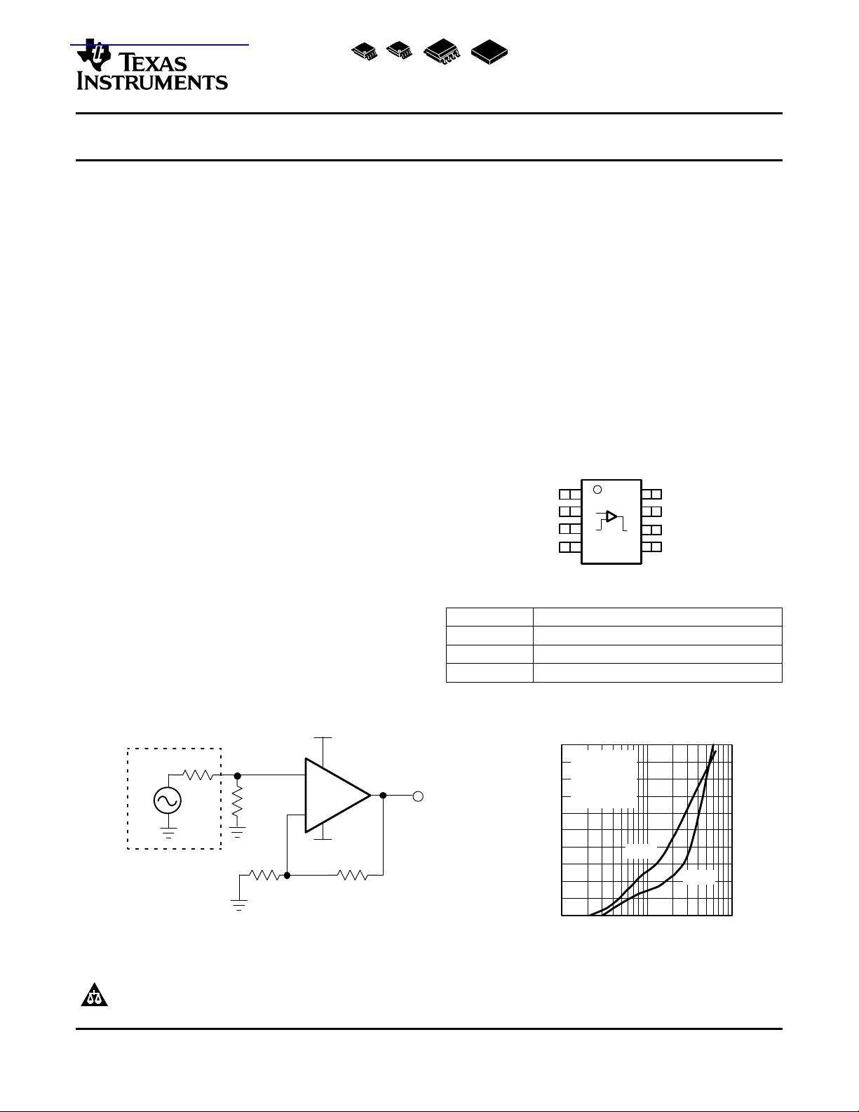
Low-Distortion, Wideband Application Circuit
NOTE: Power supply decoupling capacitors not shown
V
O
392 Ω
50 Ω
THS4211
-100
-95
-90
-85
-80
-75
-70
-65
-60
-55
-50
1 10 100
Harmonic Distortion - dBc
HARMONIC DISTORTION
vs
FREQUENCY
f - Frequency - MHz
Gain = 2
Rf = 392 Ω
RL = 150 Ω
VO = 2 V
PP
VS = ±5 V
HD2
HD3
查询THS4211DG4供应商
SLOS400D – SEPTEMBER 2002 – REVISED NOVEMBER 2004
LOW-DISTORTION, HIGH-SPEED, VOLTAGE FEEDBACK AMPLIFIER
FEATURES DESCRIPTION
• Unity Gain Stability
• Wide Bandwidth: 1 GHz
• High Slew Rate: 970 V/µs
• Low Distortion
– –90 dBc THD at 30 MHz capability. The combination of high slew rate, wide
– 130 MHz Bandwidth (0.1 dB, G = 2)
– 0.007% Differential Gain
– 0.003 ° Differential Phase
• High Output Drive, IO= 200 mA
• Excellent Video Performance without the stability concerns of decompensated
– 130 MHz Bandwidth (0.1 dB, G = 2)
– 0.007% Differential Gain
– 0.003 ° Differential Phase
• Supply Voltages
– +5 V, ± 5 V, +12 V, +15 V
• Power Down Functionality (THS4215)
• Evaluation Module Available
The THS4211 and THS4215 are high slew rate, unity
gain stable voltage feedback amplifiers designed to
run from supply voltages as low as 5 V and as high
as 15 V. The THS4215 offers the same performance
as the THS4211 with the addition of power-down
bandwidth, low distortion, and unity gain stability
make the THS4211 and THS4215 high performance
devices across multiple ac specifications.
Designers using the THS4211 are rewarded with
higher dynamic range over a wider frequency band
amplifiers. The devices are available in SOIC, MSOP
with PowerPAD™, and leadless MSOP with
PowerPAD packages.
THS4211
THS4215
APPLICATIONS
• High Linearity ADC Preamplifier
• Differential to Single-Ended Conversion
• DAC Output Buffer
• Active Filtering
• Video Applications
PowerPAD is a trademark of Texas Instruments.
PRODUCTION DATA information is current as of publication date.
Products conform to specifications per the terms of the Texas
Instruments standard warranty. Production processing does not
necessarily include testing of all parameters.
Please be aware that an important notice concerning availability, standard warranty, and use in critical applications of Texas
Instruments semiconductor products and disclaimers thereto appears at the end of this data sheet.
RELATED DEVICES
DEVICE DESCRIPTION
THS4271 1.4 GHz voltage feedback amplifier
THS4503 Wideband fully differential amplifier
THS3202 Dual, wideband current feedback amplifier
Copyright © 2002–2004, Texas Instruments Incorporated
www.ti.com
THS4211
THS4215
SLOS400D – SEPTEMBER 2002 – REVISED NOVEMBER 2004
This integrated circuit can be damaged by ESD. Texas Instruments recommends that all integrated
circuits be handled with appropriate precautions. Failure to observe proper handling and installation
procedures can cause damage.
ESD damage can range from subtle performance degradation to complete device failure. Precision
integrated circuits may be more susceptible to damage because very small parametric changes could
cause the device not to meet its published specifications.
ABSOLUTE MAXIMUM RATINGS
over operating free-air temperature range (unless otherwise noted)
Supply voltage, V
Input voltage, V
Output current, I
Continuous power dissipation See Dissipation Rating Table
Maximum junction temperature, T
Maximum junction temperature, continuous operation, long term reliability T
Storage temperature range, T
Lead temperature 1,6 mm (1/16 inch) from case for 10 seconds 300 ° C
ESD ratings CDM 1500 V
(1) Stresses above these ratings may cause permanent damage. Exposure to absolute maximum conditions for extended periods may
degrade device reliability. These are stress ratings only, and functional operation of the device at these or any other conditions beyond
those specified is not implied.
(2) The absolute maximum ratings under any condition is limited by the constraints of the silicon process. Stresses above these ratings may
cause permanent damage. Exposure to absolute maximum conditions for extended periods may degrade device reliability. These are
stress ratings only, and functional operation of the device at these or any other conditions beyond those specified is not implied.
(3) The maximum junction temperature for continuous operation is limited by package constraints. Operation above this temperature may
result in reduced reliability and/or lifetime of the device.
S
I
O
(2)
J
stg
HBM 4000 V
MM 200 V
(1)
UNIT
16.5 V
± V
S
100 mA
150 ° C
(3)
J
125 ° C
–65 ° C to 150 ° C
PACKAGE DISSIPATION RATINGS
PACKAGE
(1)
θ
JC
( ° C/W) ( ° C/W)
(2)
θ
JA
POWER RATING
(3)
TA≤ 25 ° C TA= 85 ° C
D (8 pin) 38.3 97.5 1.02 W 410 mW
DGN (8 pin)
(1)
4.7 58.4 1.71 W 685 mW
DGK (8 pin) 54.2 260 385 mW 154 mW
DRB (8 pin) 5 45.8 2.18 W 873 mW
(1) The THS4211/5 may incorporate a PowerPAD™ on the underside of the chip. This acts as a heat sink and must be connected to a
thermally dissipative plane for proper power dissipation. Failure to do so may result in exceeding the maximum junction temperature
which could permanently damage the device. See TI technical briefs SLMA002 and SLMA004 for more information about utilizing the
PowerPAD thermally enhanced package.
(2) This data was taken using the JEDEC standard High-K test PCB.
(3) Power rating is determined with a junction temperature of 125 ° C. This is the point where distortion starts to substantially increase.
Thermal management of the final PCB should strive to keep the junction temperature at or below 125 ° C for best performance and long
term reliability.
RECOMMENDED OPERATING CONDITIONS
MIN MAX UNIT
Supply voltage, (V
and VS–) V
S+
Input common-mode voltage range VS–+ 1.2 V
2
Dual supply ± 2.5 ± 7.5
Single supply 5 15
– 1.2 V
S+
www.ti.com
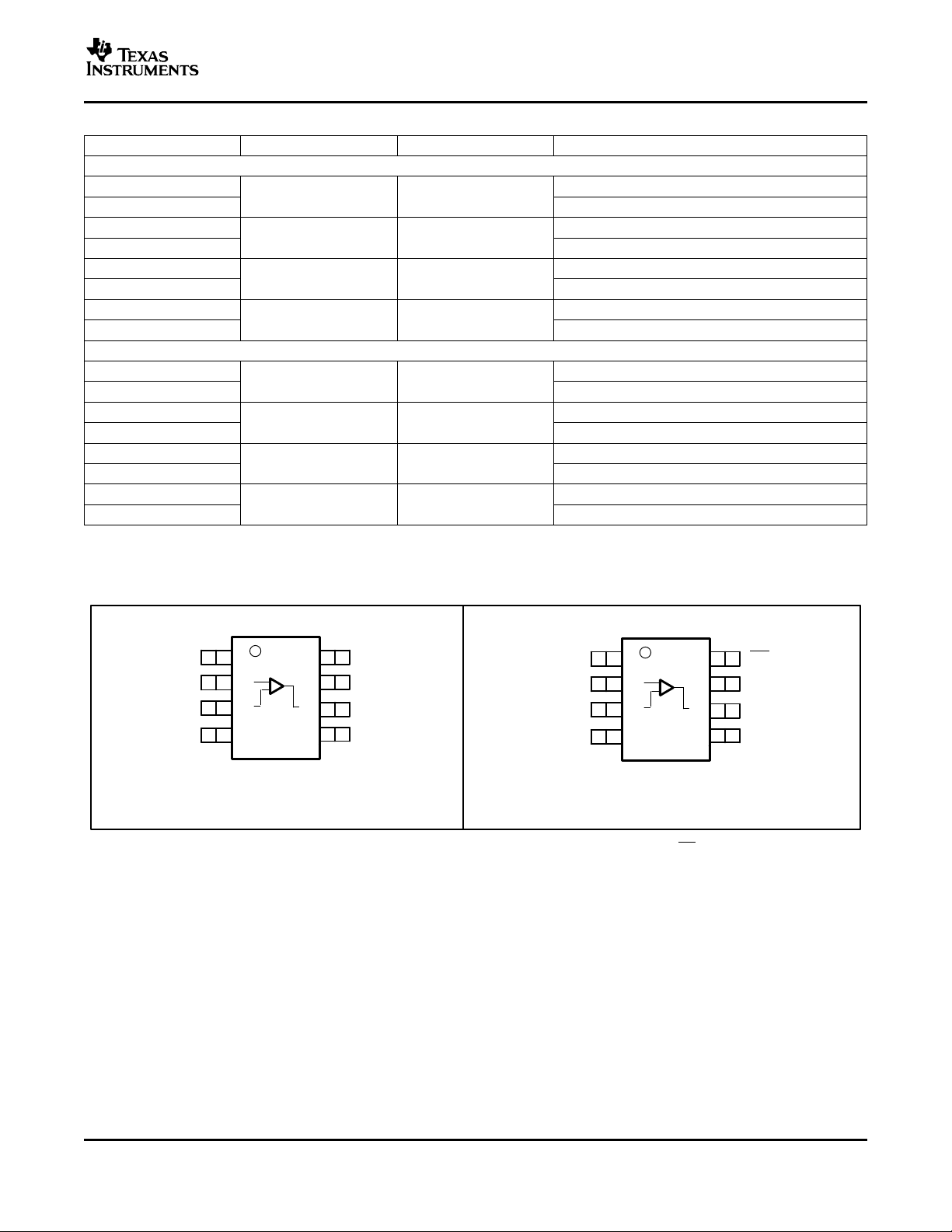
(TOP VIEW)
D, DRB, DGK, DGN
(TOP VIEW)
D, DRB, DGK, DGN
1
NC NC
THS4211
2
3
4
8
7
6
5
IN-
IN+
V
S-
VS+
V
OUT
NC
1
REF PD
THS4215
2
3
4
8
7
6
5
IN-
IN+
V
S-
VS+
V
OUT
NC
NC = No Connetion
NC = No Connection
See Note A.
SLOS400D – SEPTEMBER 2002 – REVISED NOVEMBER 2004
PACKAGING/ORDERING INFORMATION
PACKAGED DEVICES PACKAGE TYPE PACKAGE MARKING TRANSPORT MEDIA, QUANTITY
Non-power-down
THS4211D Rails, 75
THS4211DR Tape and Reel, 2500
THS4211DGK Rails, 100
THS4211DGKR Tape and Reel, 2500
THS4211DRBT Tape and Reel, 250
THS4211DRBR Tape and Reel, 3000
THS4211DGN Rails, 80
THS4211DGNR Tape and Reel, 2500
Power-down
THS4215D Rails, 75
THS4215DR Tape and Reel, 2500
THS4215DGK Rails, 100
THS4215DGKR Tape and Reel, 2500
THS4215DRBT Tape and Reel, 250
THS4215DRBR Tape and Reel, 3000
THS4215DGN Rails, 80
THS4215DGNR Tape and Reel, 2500
(1) The PowerPAD is electrically isolated from all other pins.
SOIC-8 —
MSOP-8 BEJ
QFN-8-PP
MSOP-8-PP
MSOP-8 BEZ
QFN-8-PP
MSOP-8-PP
(1)
(1)
SOIC-8 —
(1)
(1)
BET
BFN
BEU
BFQ
THS4211
THS4215
NOTE A: The devices with the power down option defaults to the ON state if no signal is applied to the PD pin.
PIN ASSIGNMENTS
3
www.ti.com
THS4211
THS4215
SLOS400D – SEPTEMBER 2002 – REVISED NOVEMBER 2004
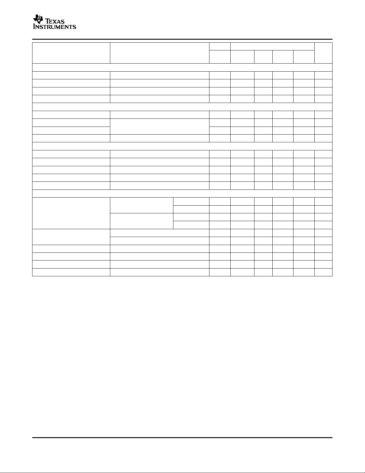
ELECTRICAL CHARACTERISTICS, V
S
= ± 5 V
RF= 392 Ω , RL= 499 Ω , G = +2, unless otherwise noted
TYP OVER TEMPERATURE
PARAMETER TEST CONDITIONS TYP/
25 ° C 25 ° C UNITS
AC PERFORMANCE
G = 1, P
G = –1, P
Small signal bandwidth G = 2, P
G = 5, P
G = 10, P
0.1 dB flat bandwidth G = 1, P
= –7 dBm 1 GHz Typ
OUT
= –16 dBm 325 MHz Typ
OUT
= –16 dBm 325 MHz Typ
OUT
= –16 dBm 70 MHz Typ
OUT
= –16 dBm 35 MHz Typ
OUT
= –7 dBm 70 MHz Typ
OUT
Gain bandwidth product G > 10 , f = 1 MHz 350 MHz Typ
Full-power bandwidth G = –1, VO= 2 V
Slew rate
Settling time to 0.1% 22 ns Typ
Settling time to 0.01% 55 ns Typ
G = 1, VO= 2 V Step 970 V/µs Typ
G = –1, VO= 2 V Step 850 V/µs Typ
G = –1, VO= 4 V Step
p
77 MHz Typ
Harmonic distortion
2nd-order harmonic distortion
G = 1, VO= 1 VPP,
f = 30 MHz
3rd-order harmonic distortion
RL= 150 Ω –78 dBc Typ
RL= 499 Ω –90 dBc Typ
RL= 150 Ω –100 dBc Typ
RL= 499 Ω –100 dBc Typ
Harmonic distortion
2nd-order harmonic distortion
G = 2, VO= 2 VPP,
f = 30 MHz
3rd-order harmonic distortion
3rd-order intermodulation (IMD
3rd-order output intercept (OIP
Differential gain (NTSC, PAL) 0.007 % Typ
Differential phase (NTSC, PAL) 0.003 ° Typ
) G = 2, VO= 2 VPP, RL= 150 Ω , f = 70 MHz –53 dBc Typ
3
) G = 2, VO= 2 VPP, RL= 150 Ω , f = 70 MHz 32 dBm Typ
3
G = 2, RL= 150 Ω
RL= 150 Ω –68 dBc Typ
RL= 499 Ω –70 dBc Typ
RL= 150 Ω –80 dBc Typ
RL= 499 Ω –82 dBc Typ
Input voltage noise f = 1 MHz 7 nV/ √ Hz Typ
Input current noise f = 10 MHz 4 pA √ Hz Typ
DC PERFORMANCE
Open-loop voltage gain (A
) VO= ± 0.3 V, RL= 499 Ω 70 65 62 60 dB Min
OL
Input offset voltage 3 12 14 14 mV Max
Average offset voltage drift ± 40 ± 40 µV/ ° C Typ
Input bias current 7 15 18 20 µA Max
Average bias current drift ± 10 ± 10 nA/ ° C Typ
V
= 0 V
CM
Input offset current 0.3 6 7 8 µA Max
Average offset current drift ± 10 ± 10 nA/ ° C Typ
0 ° C to –40 ° C
70 ° C to 85 ° C
MIN/
MAX
4
www.ti.com
THS4211
THS4215
SLOS400D – SEPTEMBER 2002 – REVISED NOVEMBER 2004
TYP OVER TEMPERATURE
PARAMETER TEST CONDITIONS TYP/
25 ° C 25 ° C UNITS
INPUT CHARACTERISTICS
Common-mode input range ± 4 ± 3.8 ± 3.7 ± 3.6 V Min
Common-mode rejection ratio V
= ± 1 V 56 52 50 48 dB Min
CM
Input resistance Common-mode 4 M Ω Typ
Input capacitance Common-mode/differential 0.3/0.2 pF Typ
OUTPUT CHARACTERISTICS
Output voltage swing ± 4.0 ± 3.8 ± 3.7 ± 3.6 V Min
Output current (sourcing) 220 200 190 180 mA Min
Output current (sinking) 170 140 130 120 mA Min
RL= 10 Ω
Output impedance f = 1 MHz 0.3 Ω Typ
POWER SUPPLY
Specified operating voltage ± 5 ± 7.5 ± 7.5 ± 7.5 V Max
Maximum quiescent current 19 22 23 24 mA Max
Minimum quiescent current 19 16 15 14 mA Min
Power supply rejection (+PSRR) V
Power supply rejection (–PSRR) V
= 5.5 V to 4.5 V, V
S+
= 5 V, V
S+
= 5 V 64 58 54 54 dB Min
S–
= –5.5 V to –4.5 V 65 60 56 56 dB Min
S–
POWER-DOWN CHARACTERISTICS (THS4215 ONLY)
Enable REF+1.8 V Min
Power-down REF+1 V Max
Enable REF–1 V Min
Power-down REF–1.5 V Max
Power-down voltage level
Power-down quiescent current
Turnon time delay(t
Turnoff time delay (t
REF = 0 V, or V
REF = V
S–
or Floating
S+
PD = Ref +1.0 V, Ref = 0 V 650 850 900 1000 µA Max
PD = Ref –1.5 V, Ref = 5 V 450 650 800 900 µA Max
) 50% of final supply current value 4 µs Typ
(ON)
) 50% of final supply current value 3 µs Typ
(Off)
Input impedance 4 G Ω Typ
Output impedance f = 1 MHz 250 k Ω Typ
0 ° C to –40 ° C
70 ° C to 85 ° C
MIN/
MAX
5
www.ti.com
THS4211
THS4215
SLOS400D – SEPTEMBER 2002 – REVISED NOVEMBER 2004
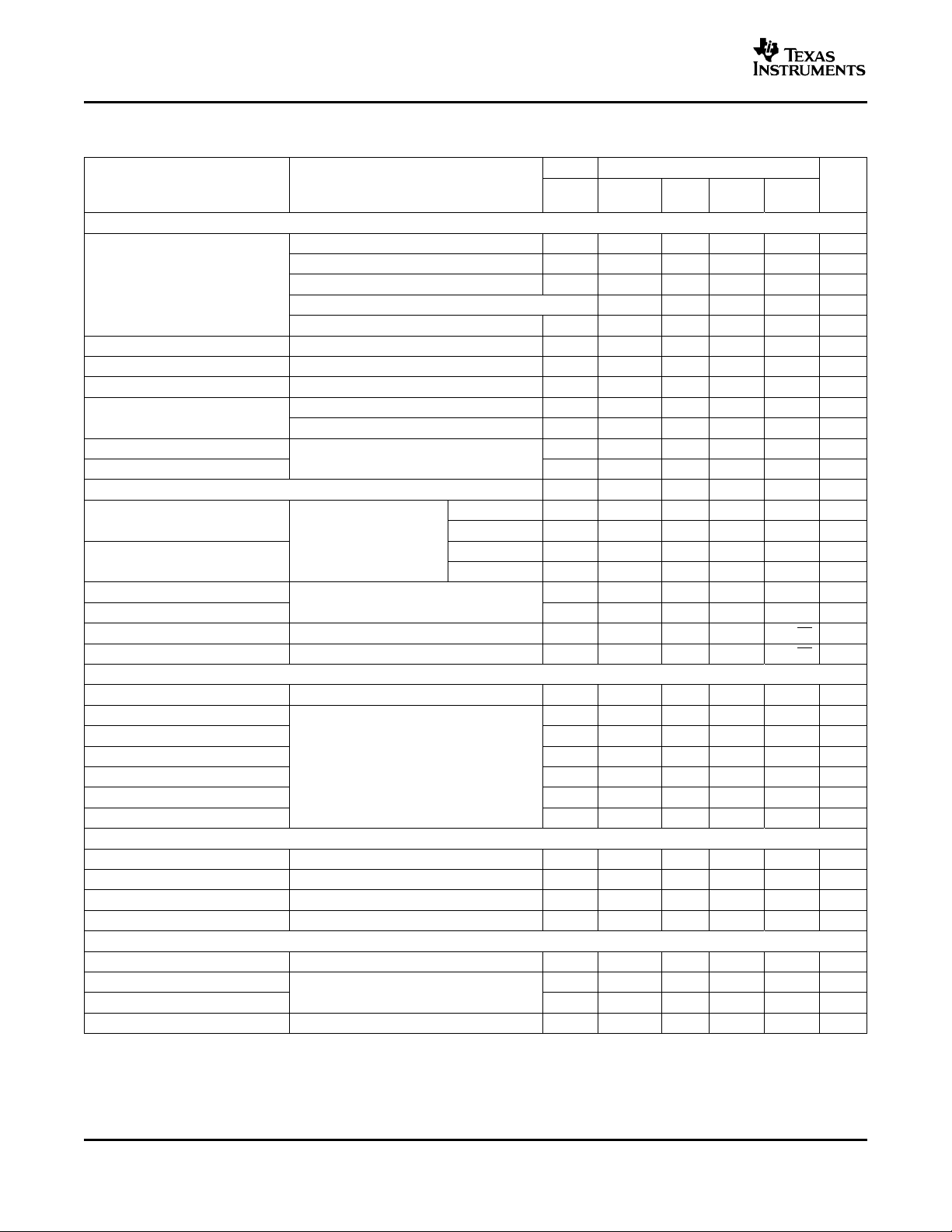
ELECTRICAL CHARACTERISTICS, V
= 5 V
S
RF= 392 Ω , RL= 499 Ω , G = +2, unless otherwise noted
TYP OVER TEMPERATURE
PARAMETER TEST CONDITIONS TYP/
25 ° C 25 ° C UNITS
AC PERFORMANCE
G = 1, P
G = –1, P
Small signal bandwidth G = 2, P
G = 5, P
G = 10, P
0.1 dB flat bandwidth G = 1, P
= –7 dBm 980 MHz Typ
OUT
= –16 dBm 300 MHz Typ
OUT
= –16 dBm 300 MHz Typ
OUT
= –16 dBm 65 MHz Typ
OUT
= –16 dBm 30 MHz Typ
OUT
= –7 dBm 90 MHz Typ
OUT
Gain bandwidth product G > 10, f = 1 MHz 300 MHz Typ
Full-power bandwidth G = –1, VO= 2 V
Slew rate
Settling time to 0.1% 22 ns Typ
Settling time to 0.01% 84 ns Typ
G = 1, VO= 2 V Step 800 V/µs Typ
G = –1, VO= 2 V Step 750 V/µs Typ
G = –1, VO= 2 V Step
p
64 MHz Typ
Harmonic distortion
2nd-order harmonic distortion
3rd-order harmonic distortion
3rd-order intermodulation (IMD
3rd-order output intercept (OIP
G = 1, VO= 1 VPP,
f = 30 MHz
) –70 dBc Typ
3
G = 1, VO= 1 VPP, RL= 150 Ω , f = 70 MHz
) 34 dBm Typ
3
RL= 150 Ω –60 dBc Typ
RL= 499 Ω –60 dBc Typ
RL= 150 Ω –68 dBc Typ
RL= 499 Ω –68 dBc Typ
Input-voltage noise f = 1 MHz 7 nV/ √ Hz Typ
Input-current noise f = 10 MHz 4 pA/ √ Hz Typ
DC PERFORMANCE
Open-loop voltage gain (A
) VO= ± 0.3 V, RL= 499 Ω 68 63 60 60 dB Min
OL
Input offset voltage 3 12 14 14 mV Max
Average offset voltage drift ± 40 ± 40 µV/ ° C Typ
Input bias current 7 15 17 18 µA Max
Average bias current drift ± 10 ± 10 nA/ ° C Typ
V
= VS/2
CM
Input offset current 0.3 6 7 8 µA Max
Average offset current drift ± 10 ± 10 nA/ ° C Typ
INPUT CHARACTERISTICS
Common-mode input range 1/4 1.2/3.8 1.3/3.7 1.4/3.6 V Min
Common-mode rejection ratio V
= ± 0.5 V, VO= 2.5 V 54 50 48 45 dB Min
CM
Input resistance Common-mode 4 M Ω Typ
Input capacitance Common-mode/differential 0.3/0.2 pF Typ
OUTPUT CHARACTERISTICS
Output voltage swing 1/4 1.2/3.8 1.3/3.7 1.4/3.6 V Min
Output current (sourcing) 230 210 190 180 mA Min
Output current (sinking) 150 120 100 90 mA Min
RL= 10 Ω
Output impedance f = 1 MHz 0.3 Ω Typ
0 ° C to –40 ° C
70 ° C to 85 ° C
MIN/
MAX
6
www.ti.com
THS4211
THS4215
SLOS400D – SEPTEMBER 2002 – REVISED NOVEMBER 2004
TYP OVER TEMPERATURE
PARAMETER TEST CONDITIONS TYP/
25 ° C 25 ° C UNITS
POWER SUPPLY
Specified operating voltage 5 15 15 15 V Max
Maximum quiescent current 19 22 23 24 mA Max
Minimum quiescent current 19 16 15 14 mA Min
Power supply rejection (+PSRR) V
Power supply rejection (–PSRR) V
= 5.5 V to 4.5 V, V
S+
= 5 V, V
S+
= 0 V 63 58 54 54 dB Min
S–
= –0.5 V to 0.5 V 65 60 56 56 dB Min
S–
POWER-DOWN CHARACTERISTICS (THS4215 ONLY)
Enable REF+1.8 V Min
Power down REF+1 V Max
Enable REF–1 V Min
Power down REF–1.5 V Max
Power-down voltage level
REF = 0 V, or V
REF = VS+or floating
S–
Power-down quiescent current PD = Ref +1.0 V, Ref = 0 V 450 650 750 850 µA Max
Power-down quiescent current PD = Ref –1.5 V, Ref = 5 V 400 650 750 850 µA Max
Turnon-time delay(t
Turnoff-time delay (t
) 4 µs Typ
(ON)
) 3 µns Typ
(Off)
50% of final value
Input impedance 6 G Ω Typ
Output impedance f = 1 MHz 75 k Ω Typ
0 ° C to –40 ° C
70 ° C to 85 ° C
MIN/
MAX
7

www.ti.com
THS4211
THS4215
SLOS400D – SEPTEMBER 2002 – REVISED NOVEMBER 2004
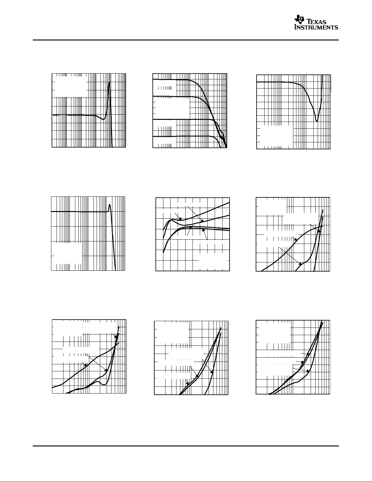
TYPICAL CHARACTERISTICS
Table of Graphs ( ± 5 V)
FIGURE
Small-signal unity gain frequency response 1
Small-signal frequency response 2
0.1 dB gain flatness frequency response 3
Large-signal frequency response 4
Slew rate vs Output voltage 5
Harmonic distortion vs Frequency 6, 7, 8, 9
Harmonic distortion vs Output voltage swing 10, 11, 12, 13
3rd-order intermodulation distortion vs Frequency 14, 16
3rd-order output intercept point vs Frequency 15, 17
Voltage and current noise vs Frequency 18
Differential gain vs Number of loads 19
Differential phase vs Number of loads 20
Settling time 21
Quiescent current vs supply voltage 22
Output voltage vs Load resistance 23
Frequency response vs Capacitive load 24
Open-loop gain and phase vs Frequency 25
Open-loop gain vs Case temperature 26
Rejection ratios vs Frequency 27
Rejection ratios vs Case temperature 28
Common-mode rejection ratio vs Input common-mode range 29
Input offset voltage vs Case temperature 30
Input bias and offset current vs Case temperature 31
Small signal transient response 32
Large signal transient response 33
Overdrive recovery 34
Closed-loop output impedance vs Frequency 35
Power-down quiescent current vs Supply voltage 36
Power-down output impedance vs Frequency 37
Turnon and turnoff delay times 38
8
www.ti.com
THS4211
THS4215
SLOS400D – SEPTEMBER 2002 – REVISED NOVEMBER 2004
Table of Graphs (5 V)
FIGURE
Small-signal unity gain frequency response 39
Small-signal frequency response 40
0.1 dB gain flatness frequency response 41
Large signal frequency response 42
Slew rate vs Output voltage 43
Harmonic distortion vs Frequency 44, 45, 46, 47
Harmonic distortion vs Output voltage swing 48, 49, 50, 51
3rd-order intermodulation distortion vs Frequency 52, 54
3rd-order intercept point vs Frequency 53, 55
Voltage and current noise vs Frequency 56
Settling time 57
Quiescent current vs Supply voltage 58
Output voltage vs Load resistance 59
Frequency response vs Capacitive load 60
Open-loop gain and phase vs Frequency 61
Open-loop gain vs Case temperature 62
Rejection ratios vs Frequency 63
Rejection ratios vs Case temperature 64
Common-mode rejection ratio vs Input common-mode range 65
Input offset voltage vs Case temperature 66
Input bias and offset current vs Case temperature 67
Small signal transient response 68
Large signal transient response 69
Overdrive recovery 70
Closed-loop output impedance vs Frequency 71
Power-down quiescent current vs Supply voltage 72
Power-down output impedance vs Frequency 73
Turnon and turnoff delay times 74
9
www.ti.com
-4
-3
-2
-1
0
1
2
3
4
5
100 k 1 M 10 M 100 M 1 G 10 G
f - Frequency - Hz
Small Signal Gain - dB
Gain = 1
RL = 499 Ω
VO = 250 mV
VS = ±5 V
-4
-2
0
2
4
6
8
10
12
14
16
18
20
22
100 k 1 M 10 M 100 M 1 G
f - Frequency - Hz
Small Signal Gain - dB
Gain = 10
Gain = 5
Gain = 2
Gain = -1
RL = 499 Ω
Rf = 392 Ω
VO = 250 mV
VS = ±5 V
-1
-0.9
-0.8
-0.7
-0.6
-0.5
-0.4
-0.3
-0.2
-0.1
0
0.1
Gain = 1
RL = 499 Ω
VO = 250 mV
VS = ±5 V
f - Frequency - Hz
Small Signal Gain - dB
1 M
10 M 100 M
1 G
100 k 1 M 10 M 100 M 1 G
f - Frequency - Hz
Large Signal Gain - dB
Gain = 1
RL = 499 Ω
VO = 2 V
PP
VS = ±5 V
-4
-3
-2
-1
0
1
-100
-95
-90
-85
-80
-75
-70
-65
-60
1 10 100
Harmonic Distortion - dBc
f - Frequency - MHz
Gain = 1
VO = 1 V
PP
VS = ±5 V
HD2, RL = 150 Ω
HD3, RL = 150 Ω
and RL = 499 Ω
HD2, RL = 499 Ω
0 0.5 1 1.5 2 2.5 3 3.5 4 4.5 5
V
O
- Output Voltage - V
SR - Slew Rate -
sµ
V/
RL = 499 Ω
Rf = 392 Ω
VS = ±5 V
0
200
400
600
800
1000
1200
1400
Fall, Gain = 1
Rise, Gain = 1
Fall, Gain =- 1
Rise, Gain = -1
-100
-95
-90
-85
-80
-75
-70
-65
-60
-55
-50
1
10
100
Harmonic Distortion - dBc
f - Frequency - MHz
Gain = 1
VO = 2 V
PP
VS = ±5 V
HD3, RL = 150 Ω
and RL = 499 Ω
HD2, RL = 150 Ω
HD2, RL = 499 Ω
HD3, RL = 150Ω,
and RL = 499 Ω
Harmonic Distortion - dBc
f - Frequency - MHz
-100
-95
-90
-85
-80
-75
-70
-65
-60
-55
-50
1 10 100
HD2, RL = 150Ω
HD2, RL = 499Ω
Gain = 2
Rf = 392 Ω
VO = 2 V
PP
VS = ±5 V
-100
-95
-90
-85
-80
-75
-70
-65
-60
-55
1 10 100
Harmonic Distortion - dBc
f - Frequency - MHz
Gain = 2
Rf = 392 Ω
VO = 1 V
PP
VS = ±5 V
HD2, RL = 499Ω
HD2, RL = 150Ω
HD3, RL = 150Ω,
and RL = 499 Ω
THS4211
THS4215
SLOS400D – SEPTEMBER 2002 – REVISED NOVEMBER 2004
TYPICAL CHARACTERISTICS ( ± 5 V Graphs)
SMALL SIGNAL UNITY GAIN SMALL SIGNAL FREQUENCY 0.1 dB GAIN FLATNESS
FREQUENCY RESPONSE RESPONSE FREQUENCY RESPONSE
Figure 1. Figure 2. Figure 3.
LARGE SIGNAL FREQUENCY vs vs
SLEW RATE HARMONIC DISTORTION
RESPONSE OUTPUT VOLTAGE FREQUENCY
Figure 4. Figure 5. Figure 6.
HARMONIC DISTORTION HARMONIC DISTORTION HARMONIC DISTORTION
vs vs vs
FREQUENCY FREQUENCY FREQUENCY
10
Figure 7. Figure 8. Figure 9.
www.ti.com
-100
-95
-90
-85
-80
-75
-70
0 0.5 1 1.5 2 2.5 3 3.5 4 4.5 5
Harmonic Distortion - dBc
VO - Output Voltage Swing - ±V
HD2, RL = 499Ω
HD3, RL = 150Ω
HD2, RL = 150Ω
HD3, RL = 499Ω
Gain = 1
f= 8 MHz
VS = ±5 V
Harmonic Distortion - dBc
VO - Output Voltage Swing - ±V
Gain = 1
f= 32 MHz
VS = ±5 V
HD2, RL = 499Ω
HD2, RL = 150Ω
HD3, RL = 150Ω
HD3, RL = 499Ω
-100
-95
-90
-85
-80
-75
-70
-65
-60
-55
-50
0 0.5 1 1.5 2 2.5 3 3.5 4 4.5 5
-100
-95
-90
-85
-80
-75
-70
-65
0 0.5 1 1.5 2 2.5 3 3.5 4 4.5 5
Harmonic Distortion - dBc
VO - Output Voltage Swing - ±V
Gain = 2
Rf = 249 Ω
f = 8 MHz
VS = ±5 V
HD3, RL = 150Ω
HD2, RL = 499Ω
HD3, RL = 499Ω
HD2, RL = 150Ω
-100
-95
-90
-85
-80
-75
-70
-65
-60
-55
-50
-45
-40
0 1 2 3 4 5
Harmonic Distortion - dBc
VO - Output Voltage Swing - ±V
Gain = 2
Rf = 249 Ω
f = 32 MHz
VS = ±5 V
HD3, RL = 150Ω
HD2, RL = 499Ω
HD2, RL = 150Ω
HD3, RL = 499Ω
0.5 1.5 2.5 3.5 4.5
30
35
40
45
50
55
60
0 20 40 60 80 100
VO = 2 V
PP
VO = 1 V
PP
Gain = 1
RL = 150 Ω
VS =±5 V
200 kHz Tone Spacing
Third-Order Output Intersept Point - dBm
f - Frequency - MHz
-100
-95
-90
-85
-80
-75
-70
-65
-60
-55
-50
-45
10 100
Third-Order Intermodulation Distortion - dBc
f - Frequency - MHz
VO = 2 V
PP
VO = 1 V
PP
Gain = 1
RL = 150 Ω
VS =±5 V
200 kHz Tone Spacing
1
10
100
1 k 10 k 100 k 1 M 10 M 100 M
1
10
100
V
n
I
n
f - Frequency - Hz
- Voltage Noise - nV/ Hz
V
n
- Current Noise - pA/ Hz
I
n
Third-Order Intermodulation Distortion - dBc
f - Frequency - MHz
Gain = 2
RL = 150 Ω
VS =±5 V
200 kHz Tone Spacing
VO = 2 V
PP
VO = 1 V
PP
-100
-95
-90
-85
-80
-75
-70
-65
-60
-55
-50
-45
-40
10 100
20
25
30
35
40
45
50
55
60
0 20 40 60 80 100
Third-Order Output Intersept Point - dBm
f - Frequency - MHz
Gain = 2
RL = 150 Ω
VS = ±5 V
200 kHz Tone Spacing
VO = 1 V
PP
VO = 2 V
PP
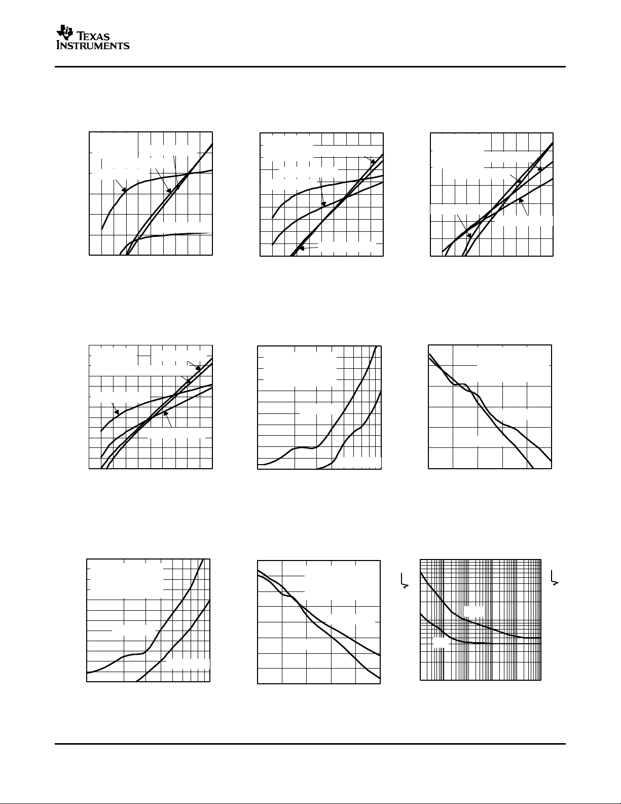
TYPICAL CHARACTERISTICS ( ± 5 V Graphs) (continued)
THS4211
THS4215
SLOS400D – SEPTEMBER 2002 – REVISED NOVEMBER 2004
HARMONIC DISTORTION HARMONIC DISTORTION HARMONIC DISTORTION
vs vs vs
OUTPUT VOLTAGE SWING OUTPUT VOLTAGE SWING OUTPUT VOLTAGE SWING
Figure 10. Figure 11. Figure 12.
THIRD ORDER INTERMODULATION THIRD ORDER OUTPUT
HARMONIC DISTORTION DISTORTION INTERCEPT POINT
vs vs vs
OUTPUT VOLTAGE SWING FREQUENCY FREQUENCY
THIRD ORDER INTERMODULATION THIRD ORDER OUTPUT
Figure 13. Figure 14. Figure 15.
DISTORTION INTERCEPT POINT VOLTAGE AND CURRENT NOISE
vs vs vs
FREQUENCY FREQUENCY FREQUENCY
Figure 16. Figure 17. Figure 18.
11
www.ti.com
0
0.02
0.04
0.06
0.08
0.10
0.12
0.14
0.16
0.18
0.20
0 1 2 3 4 5 6 7 8
Number of Loads - 150 Ω
Differential Phase -
Gain = 2
Rf = 392 Ω
VS = ±5 V
40 IRE - NTSC and Pal
Worst Case ±100 IRE Ramp
NTSC
PAL
°
Number of Loads - 150 Ω
Differential Gain - %
NTSC
PAL
0
0.005
0.010
0.015
0.020
0.025
0.030
0 1 2 3 4 5 6 7 8
Gain = 2
Rf = 392 Ω
VS = ±5 V
40 IRE - NTSC and Pal
Worst Case ±100 IRE Ramp
-3
-2
-1
0
1
2
3
0 5 10 15 20 25
t - Time - ns
- Output Voltage - VV
O
Rising Edge
Falling Edge
Gain = -1
RL = 499 Ω
Rf = 392 Ω
f= 1 MHz
VS = ±5 V
-5
-4
-3
-2
-1
0
1
2
3
4
5
10 100 1000
R
L
- Load Resistance - Ω
- Output Voltage - VV
O
TA = -40 to 85°C
10
12
14
16
18
20
22
2.5 3 3.5 4 4.5 5
TA = -40°C
V
S
- Supply Voltage - ±V
Quiescent Current - mA
TA = 85°C
TA = 25°C
-3
-2.5
-2
-1.5
-1
-0.5
0
0.5
1
100 k 1 M 10 M 100 M 1 G
Capacitive Load - Hz
Normalized Gain - dB
R
(ISO)
= 15 Ω
CL = 50 pF
VS =±5 V
R
(ISO)
= 10 Ω
CL = 100 pF
R
(ISO)
= 25 Ω
CL = 10 pF
60
65
70
75
80
85
90
2.5 3 3.5 4 4.5 5
Open-Loop Gain - dB
Case Temperature - °C
TA = -40°C
TA = 85°C
TA = 25°C
0
10
20
30
40
50
60
70
100 k 1 M 10 M 100 M 1 G
CMRR
VS = ±5 V
Rejection Ratios - dB
f - Frequency - Hz
PSRR+
PSRR-
80
-10
0
10
20
30
40
50
60
70
10 k 100 k 1 M 10 M 100 M 1 G
0
20
40
60
80
100
120
160
180
Open-Loop Gain - dB
f - Frequency - Hz
VS = ±5 V
Phase - °
140
THS4211
THS4215
SLOS400D – SEPTEMBER 2002 – REVISED NOVEMBER 2004
TYPICAL CHARACTERISTICS ( ± 5 V Graphs) (continued)
DIFFERENTIAL GAIN DIFFERENTIAL PHASE
vs vs
NUMBER OF LOADS NUMBER OF LOADS SETTLING TIME
Figure 19. Figure 20. Figure 21.
QUIESCENT CURRENT OUTPUT VOLTAGE FREQUENCY RESPONSE
vs vs vs
SUPPLY VOLTAGE LOAD RESISTANCE CAPACITIVE LOAD
OPEN-LOOP GAIN AND PHASE OPEN-LOOP GAIN REJECTION RATIOS
12
Figure 22. Figure 23. Figure 24.
vs vs vs
FREQUENCY CASE TEMPERATURE FREQUENCY
Figure 25. Figure 26. Figure 27.
www.ti.com
0
10
20
30
40
50
60
70
80
-40-30-20-10 0 10 20 30 40 50 60 70 80 90
Rejection Ratios - dB
Case Temperature - °C
VS = ±5 V
PSRR-
CMMR
PSRR+
0
5
10
15
20
25
30
35
40
45
50
55
60
-4.5 -3 -1.5 0 1.5 3 4.5
Input Common-Mode Range - V
CMRR - Common-Mode Rejection Ratio - dB
VS = ±5 V
TA = 25°C
0
1
2
3
4
5
6
7
8
9
-40-30-20 -10 0 10 20 30 40 50 60 70 80 90
VS = 5 V
VS = ±5 V
T
C
- Case Temperature - °C
- Input Offset Voltage - mV
V
OS
-0.12
-0.1
-0.08
-0.06
-0.04
-0.02
0.02
0.04
0.06
0.08
0.1
0.12
-1 0 1 2 3 4 5 6 7 8 9 10
t - Time - ns
- Output Voltage - VV
O
Gain = -1
RL = 499 Ω
Rf =392 Ω
tr/tf = 300 ps
VS = ±5 V
0
-1.5
-1
-0.5
0
0.5
1
1.5
-2 0 2 4 6 8 10 12 14 16 18 20
t - Time - ns
- Output Voltage - VV
O
Gain = -1
RL = 499 Ω
Rf = 392 Ω
tr/tf = 300 ps
VS = ±5 V
5.6
5.7
5.8
5.9
6
6.1
6.2
6.3
6.4
6.5
6.6
-40-30-20-10 0 10 20 30 40 50 60 70 80 90
0.2
0.25
0.3
0.35
0.4
0.45
0.5
0.55
0.6
0.65
0.7
- Input Bias Current -
TC - Case Temperature - °C
VS = ±5 V
- Input Offset Current -
I
IB-
I
IB
Aµ
I
OS
Aµ
I
IB+
I
OS
0
-6
-5
-4
-3
-2
-1
0
1
2
3
4
5
6
0 0.1 0.2 0.3 0.4 0.5 0.6 0.7 0.8 0.9 1
-3
-2.5
-2
-1.5
-1
-0.5
0.5
1
1.5
2
2.5
3
t - Time - µs
Single-Ended Output Voltage - V
- Input Voltage - VV
I
VS = ±5 V
0.01
0.1
1
10
100
1 k
10 k
100 k
100 k 1 M 10 M 100 M 1 G
f - Frequency - Hz
Closed-Loop Output Impedance - Ω
RL = 499 Ω,
RF = 392 Ω,
PIN = -4 dBm
VS = ±5 V
0
100
200
300
400
500
600
700
800
2.5 3 3.5 4 4.5 5
V
S
- Supply Voltage - ±V
Power-Down Quiescent Current -
TA = 85°C
TA = 25°C
Aµ
TA = -40°C
TYPICAL CHARACTERISTICS ( ± 5 V Graphs) (continued)
THS4211
THS4215
SLOS400D – SEPTEMBER 2002 – REVISED NOVEMBER 2004
REJECTION RATIOS COMMON-MODE REJECTION RATIO INPUT OFFSET VOLTAGE
vs vs vs
CASE TEMPERATURE INPUT COMMON-MODE RANGE CASE TEMPERATURE
Figure 28. Figure 29. Figure 30.
INPUT BIAS AND OFFSET
CURRENT
vs SMALL SIGNAL TRANSIENT LARGE SIGNAL TRANSIENT
CASE TEMPERATURE RESPONSE RESPONSE
OVERDRIVE RECOVERY FREQUENCY SUPPLY VOLTAGE
Figure 31. Figure 32. Figure 33.
CLOSED-LOOP OUTPUT POWER-DOWN QUIESCENT
IMPEDANCE CURRENT
vs vs
Figure 34. Figure 35. Figure 36.
13

www.ti.com
-0.005
0.005
0.01
0.015
0.02
0.025
0.03
0.035
0.04
-0.01 0 0.01 0.02 0.03 0.04 0.05 0.06 0.07
-7.5
-6
-4.5
-3
-1.5
0
1.5
3
4.5
6
t - Time - ns
- Output Voltage Level - VV
O
Gain = -1
RL = 499 Ω
VS = ±5 V
- Input Voltage Level - VV
I
0
0.001
0.1
10
1000
100 k 1 M 10 M 100 M 1 G 10 G
f - Frequency - Hz
Power-Down Output Impedance - Ω
Gain = 1
RL = 499 Ω
PIN = -1 dBm
VS = ±5 V
THS4211
THS4215
SLOS400D – SEPTEMBER 2002 – REVISED NOVEMBER 2004
TYPICAL CHARACTERISTICS ( ± 5 V Graphs) (continued)
POWER-DOWN
OUTPUT IMPEDANCE
vs TURNON AND TURNOFF TIMES
FREQUENCY DELAY TIME
Figure 37. Figure 38.
14

www.ti.com
-4
-2
0
2
4
6
8
10
12
14
16
18
20
22
100 k 1 M 10 M 100 M 1 G
f - Frequency - Hz
Small Signal Gain - dB
Gain = 10
Gain = 5
Gain = 2
Gain = -1
RL = 499 Ω
Rf = 392 Ω
VO = 250 mV
VS = 5 V
1 G
-4
-3
-2
-1
0
1
2
3
4
100 k 1 M 10 M 100 M 10 G
f - Frequency - Hz
Gain = 1
RL = 499 Ω
VO = 250 mV
VS = 5 V
Small Signal Gain - dB
-1
-0.9
-0.8
-0.7
-0.6
-0.5
-0.4
-0.3
-0.2
-0.1
0
0.1
1 M 10 M 100 M 1 G
f - Frequency - Hz
Gain = 1
RL = 499 Ω
V
O
= 250 mV
VS = 5 V
Small Signal Gain - dB
-100
-95
-90
-85
-80
-75
-70
-65
-60
-55
-50
1 10 100
HD2
HD3
Harmonic Distortion - dBc
f - Frequency - MHz
Gain = 1
VO = 1 V
PP
RL = 150 Ω, and 499 Ω
VS = 5 V
0
100
200
300
400
500
600
700
800
900
1000
0.4 0.6 0.8 1 1.2 1.4 1.6 1.8 2
SR - Slew Rate - V/
V
O
- Output Voltage -V
sµ
RL = 499 Ω
Rf = 392 Ω
VS = 5 V
Fall, G = 1
Rise, G = 1
Fall, G = -1
Rise, G = -1
-4
-3
-2
-1
0
1
100 K 1 M 10 M 100 M 1 G
f - Frequency - Hz
Large Signal Gain - dB
Gain = 1
RL = 499 Ω
VO = 2 V
PP
VS = 5 V
-90
-85
-80
-75
-70
-65
-60
-55
-50
-45
-40
1
10
100
HD2
HD3
Harmonic Distortion - dBc
f - Frequency - MHz
Gain = 1
VO = 2 V
PP
RL = 150 Ω, and 499 Ω
VS = 5 V
-100
-90
-80
-70
-60
-50
-40
1
10 100
HD2
HD3
Harmonic Distortion - dBc
f - Frequency - MHz
Gain = 2
VO = 1 V
PP
Rf = 392 Ω
RL = 150 Ω and 499 Ω
VS = 5 V
-90
-80
-70
-60
-50
-40
-30
1 10 100
HD2
HD3
Harmonic Distortion - dBc
f - Frequency - MHz
Gain = 2
VO = 2 V
PP
Rf = 392 Ω
RL = 150 Ω and 499 Ω
VS = 5 V
SLOS400D – SEPTEMBER 2002 – REVISED NOVEMBER 2004
TYPICAL CHARACTERISTICS (5 V Graphs)
SMALL SIGNAL UNITY GAIN SMALL SIGNAL 0.1 dB GAIN FLATNESS
FREQUENCY RESPONSE FREQUENCY RESPONSE FREQUENCY RESPONSE
Figure 39. Figure 40. Figure 41.
THS4211
THS4215
LARGE SIGNAL vs vs
SLEW RATE HARMONIC DISTORTION
FREQUENCY RESPONSE OUTPUT VOLTAGE FREQUENCY
Figure 42. Figure 43. Figure 44.
HARMONIC DISTORTION HARMONIC DISTORTION HARMONIC DISTORTION
vs vs vs
FREQUENCY FREQUENCY FREQUENCY
Figure 45. Figure 46. Figure 47.
15

www.ti.com
-100
-95
-90
-85
-80
-75
-70
-65
-60
0 0.5 1 1.5 2 2.5
Harmonic Distortion - dBc
VO - Output Voltage Swing - V
HD2
HD3
Gain = 1
RL = 150 Ω, and 499 Ω,
f = 8 MHz
VS = 5 V
-100
-95
-90
-85
-80
-75
-70
-65
-60
-55
-50
0 0.5 1 1.5 2 2.5
Harmonic Distortion - dBc
VO - Output Voltage Swing - V
HD2
HD3
Gain = 2
Rf = 392 Ω
RL = 150 Ω and 499 Ω
f = 8 MHz
VS = 5 V
Harmonic Distortion - dBc
VO - Output Voltage Swing - V
-90
-85
-80
-75
-70
-65
-60
-55
-50
-45
0 0.5 1 1.5 2 2.5
HD2
HD3
Gain = 1
RL = 150 Ω, and 499 Ω,
f = 32 MHz
VS = 5 V
Harmonic Distortion - dBc
VO - Output Voltage Swing - V
HD2
HD3
Gain = 2
Rf = 392 Ω
RL = 150 Ω and 499 Ω
f = 32 MHz
VS = 5 V
-80
-75
-70
-65
-60
-55
-50
-45
-40
0 0.5 1 1.5 2 2.5
30
35
40
45
50
0 10 20 30 40 50 60 70 80
Third-Order Output Intersept Point - dBm
f - Frequency - MHz
Gain = 1
RL = 150 Ω
VS = 5 V
200 kHz Tone Spacing
VO = 2V
PP
VO = 1V
PP
-100
-95
-90
-85
-80
-75
-70
-65
-60
-55
-50
-45
-40
10 100
Third-Order Intermodulation Distortion - dBc
f - Frequency - MHz
Gain = 1
RL = 150 Ω
VS = 5 V
200 kHz Tone
Spacing
VO = 2V
PP
VO = 1V
PP
1
10
100
1 k 10 k 100 k 1 M 10 M 100 M
1
10
100
V
n
I
n
f - Frequency - Hz
- Voltage Noise - nV/ Hz
V
n
- Current Noise - pA/ Hz
I
n
-100
-90
-80
-70
-60
-50
-40
-30
10 100
Third-Order Intermodulation Distortion - dBc
f - Frequency - MHz
Gain = 1
RL = 150 Ω
VS = 5 V
200 kHz Tone
Spacing
VO = 2 V
PP
VO = 1 V
PP
10
15
20
25
30
35
40
45
50
0 20 40 60 80 100
Third-Order Output Intersept Point - dBm
f - Frequency - MHz
Gain = 2
RL = 150 Ω
VS = 5 V
200 kHz Tone Spacing
VO = 2 V
PP
VO = 1 V
PP
THS4211
THS4215
SLOS400D – SEPTEMBER 2002 – REVISED NOVEMBER 2004
TYPICAL CHARACTERISTICS (5 V Graphs) (continued)
HARMONIC DISTORTION HARMONIC DISTORTION HARMONIC DISTORTION
vs vs vs
FREQUENCY OUTPUT VOLTAGE SWING OUTPUT VOLTAGE SWING
Figure 48. Figure 49. Figure 50.
THIRD ORDER INTERMODULATION THIRD ORDER OUTPUT INTERCEPT
HARMONIC DISTORTION DISTORTION POINT
vs vs vs
OUTPUT VOLTAGE SWING FREQUENCY FREQUENCY
THIRD ORDER INTERMODULATION THIRD ORDER OUTPUT INTERCEPT
16
Figure 51. Figure 52. Figure 53.
DISTORTION POINT VOLTAGE AND CURRENT NOISE
vs vs vs
FREQUENCY FREQUENCY FREQUENCY
Figure 54. Figure 55. Figure 56.

www.ti.com
-2
-1.5
-1
-0.5
0
0.5
1
1.5
2
10 100 1000
R
L
- Load Resistance - Ω
- Output Voltage - VV
O
TA = -40 to 85°C
-1.5
-1
-0.5
0
0.5
1
1.5
0 5 10 15 20 25
t - Time - ns
- Output Voltage - VV
O
Rising Edge
Falling Edge
Gain = -1
RL = 499 Ω
Rf = 392 Ω
f= 1 MHz
VS = 5 V
10
12
14
16
18
20
22
2.5 3 3.5 4 4.5 5
TA = -40°C
V
S
- Supply Voltage - ±V
Quiescent Current - mA
TA = 85°C
TA = 25°C
-3
-2.5
-2
-1.5
-1
-0.5
0
0.5
1
100 k 1 M 10 M 100 M 1 G
Capacitive Load - Hz
Normalized Gain - dB
R
(ISO)
= 15 Ω
CL = 50 pF
VS = 5 V
R
(ISO)
= 10 Ω
CL = 100 pF
R
(ISO)
= 25 Ω, CL = 10 pF
60
65
70
75
80
85
90
2.5 3 3.5 4 4.5 5
Open-Loop Gain - dB
Case Temperature - °C
TA = -40°C
TA = 85°C
TA = 25°C
80
-10
0
10
20
30
40
50
60
70
10 k 100 k 1 M 10 M 100 M 1 G
0
20
40
60
80
100
120
160
180
Open-Loop Gain - dB
f - Frequency - Hz
VS = 5 V
Phase - °
140
0
10
20
30
40
50
60
70
80
-40-30-20-10 0 10 20 30 40 50 60 70 80 90
Rejection Ratios - dB
Case Temperature - °C
VS = 5 V
PSRR-
CMMR
PSRR+
0
10
20
30
40
50
60
70
100 k 1 M 10 M 100 M 1 G
CMRR
VS = 5 V
Rejection Ratios - dB
f - Frequency - Hz
PSRR+
PSRR-
0
5
10
15
20
25
30
35
40
45
50
55
60
0 1 2 3 4 5
Input Common-Mode Voltage Range - V
CMRR - Common-Mode Rejection Ratio - dB
VS = 5 V
TYPICAL CHARACTERISTICS (5 V Graphs) (continued)
THS4211
THS4215
SLOS400D – SEPTEMBER 2002 – REVISED NOVEMBER 2004
QUIESCENT CURRENT OUTPUT VOLTAGE
vs vs
SETTLING TIME SUPPLY VOLTAGE LOAD RESISTANCE
Figure 57. Figure 58. Figure 59.
FREQUENCY RESPONSE OPEN-LOOP GAIN AND PHASE OPEN-LOOP GAIN
vs vs vs
CAPACITIVE LOAD FREQUENCY CASSE TEMPERATURE
REJECTION RATIOS REJECTION RATIOS COMMON-MODE REJECTION RATIO
FREQUENCY CASE TEMPERATURE INPUT COMMON-MODE RANGE
Figure 60. Figure 61. Figure 62.
vs vs vs
Figure 63. Figure 64. Figure 65.
17

www.ti.com
5.6
5.7
5.8
5.9
6
6.1
6.2
6.3
6.4
6.5
6.6
-40-30 -20-10 0 10 20 30 40 50 60 70 80 90
0.2
0.25
0.3
0.35
0.4
0.45
0.5
0.55
0.6
0.65
0.7
- Input Bias Current -
TC - Case Temperature - °C
VS = 5 V
- Input Offset Current -
I
IB-
I
IB
Aµ
I
OS
Aµ
I
IB+
I
OS
-0.12
-0.1
-0.08
-0.06
-0.04
-0.02
0.02
0.04
0.06
0.08
0.1
0.12
-1 0 1 2 3 4 5 6 7 8 9 10
t - Time - ns
- Output Voltage - VV
O
Gain = -1
RL = 499 Ω
Rf =392 Ω
tr/tf = 300 ps
VS = 5 V
0
0
1
2
3
4
5
6
7
8
9
-40-30-20 -10 0 10 20 30 40 50 60 70 80 90
VS = 5 V
VS = ±5 V
T
C
- Case Temperature - °C
- Input Offset Voltage - mV
V
OS
-1.5
-1
-0.5
0
0.5
1
1.5
-2 0 2 4 6 8 10 12 14 16 18 20
t - Time - ns
- Output Voltage - VV
O
Gain = -1
RL = 499 Ω
Rf = 392 Ω
tr/tf = 300 ps
VS = 5 V
0
-3
-2
-1
0
1
2
3
0 0.1 0.2 0.3 0.4 0.5 0.6 0.7 0.8 0.9 1
-1.5
-1
-0.5
0.5
1
1.5
t - Time - µs
Single-Ended Output Voltage - V
- Input Voltage - VV
I
VS = 5 V
0.01
0.1
1
10
100
1 k
10 k
100 k
100 k 1 M 10 M 100 M 1 G
f - Frequency - Hz
Closed-Loop Output Impedance - Ω
RL = 499 Ω,
RF = 392 Ω,
PIN = -4 dBm
VS = 5 V
t - Time - ns
- Output Voltage Level - VV
O
Gain = -1
RL = 499 Ω
VS = 5 V
- Input Voltage Level - VV
I
-0.005
0
0.005
0.01
0.015
0.02
0.025
0.03
0.035
-0.01 0 0.01 0.02 0.03 0.04 0.05 0.06 0.07
-7.5
-6
-4.5
-3
-1.5
0
1.5
3
4.5
0
100
200
300
400
500
600
700
800
2.5 3 3.5 4 4.5 5
V
S
- Supply Voltage - ±V
TA = 85°C
TA = 25°C
TA = -40°C
Power-Down Quiescent Current -
Aµ
0.001
0.1
10
1000
100 k 1 M 10 M 100 M 1 G 10 G
f - Frequency - Hz
Gain = 1
RL = 499 Ω
PIN = -1 dBm
VS = 5 V
Power-Down Output Impedance - Ω
THS4211
THS4215
SLOS400D – SEPTEMBER 2002 – REVISED NOVEMBER 2004
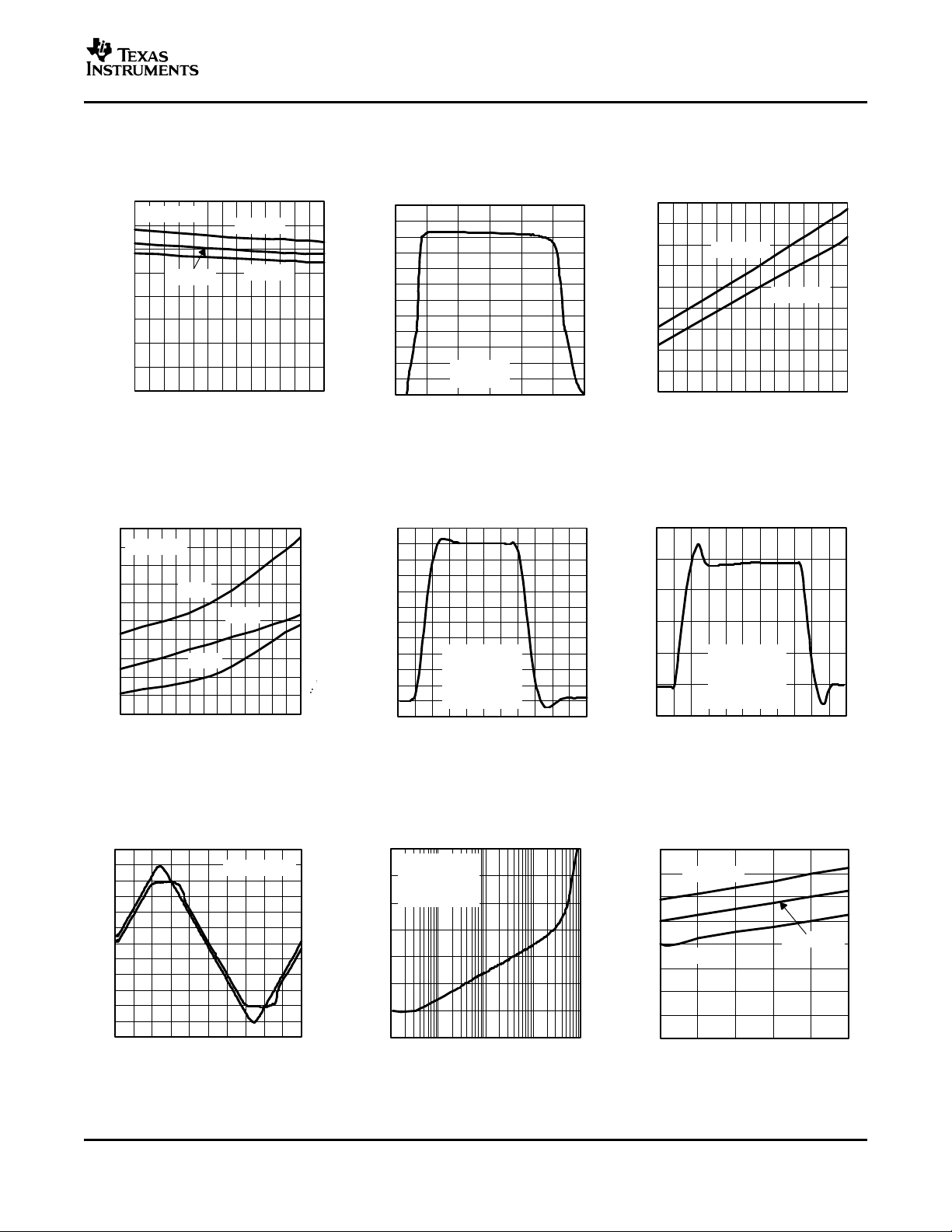
TYPICAL CHARACTERISTICS (5 V Graphs) (continued)
INPUT OFFSET VOLTAGE CURRENT
INPUT BIAS AND OFFSET
vs vs SMALL SIGNAL TRANSIENT
CASE TEMPERATURE CASE TEMPERATURE RESPONSE
Figure 66. Figure 67. Figure 68.
CLOSED-LOOP OUTPUT
IMPEDANCE
LARGE SIGNAL TRANSIENT vs
RESPONSE OVERDRIVE RECOVERY FREQUENCY
POWER-DOWN QUIESCENT POWER-DOWN OUTPUT
SUPPLY VOLTAGE FREQUENCY DELAY TIME
18
Figure 69. Figure 70. Figure 71.
CURRENT IMPEDANCE
vs vs TURNON AND TURNOFF TIMES
Figure 72. Figure 73. Figure 74.

www.ti.com
_
+
THS4211
R
f
392 Ω
49.9 Ω
100 pF
0.1 µF 6.8 µF
-V
S
-5 V
R
g
50 Ω Source
+
V
I
100 pF
0.1 µF 6.8 µF
+
+V
S
5 V
V
O
499 Ω
392 Ω
HIGH-SPEED OPERATIONAL AMPLIFIERS
The THS4211 and the THS4215 operational amplifiers set new performance levels, combining low
distortion, high slew rates, low noise, and a unity-gain
bandwidth in excess of 1 GHz. To achieve the full
performance of the amplifier, careful attention must
be paid to printed-circuit board layout and component
selection.
The THS4215 provides a power-down mode, providing the ability to save power when the amplifier is
inactive. A reference pin is provided to allow the user
the flexibility to control the threshold levels of the
power-down control pin.
Applications Section Contents
• Wideband, Noninverting Operation
• Wideband, Inverting Gain Operation
• Single Supply Operation
• Saving Power With Power-Down Functionality
and Setting Threshold Levels With the Reference
Pin
• Power Supply Decoupling Techniques and
Recommendations
• Using the THS4211 as a DAC Output Buffer
• Driving an ADC With the THS4211
• Active Filtering With the THS4211
• Building a Low-Noise Receiver With the THS4211
• Linearity: Definitions, Terminology, Circuit
Techniques and Design Tradeoffs
• An Abbreviated Analysis of Noise in Amplifiers
• Driving Capacitive Loads
• Printed-Circuit Board Layout Techniques for
Optimal Performance
• Power Dissipation and Thermal Considerations
• Performance vs Package Options
• Evaluation Fixtures, Spice Models, and
Applications Support
• Additional Reference Material
• Mechanical Package Drawings
WIDEBAND, NONINVERTING OPERATION
The THS4211 and the THS4215 are unity-gain,
stable 1-GHz voltage-feedback operational amplifiers,
with and without power-down capability, designed to
operate from a single 5-V to 15-V power supply.
Figure 75 shows the noninverting-gain configuration
of 2 V/V used to demonstrate the typical performance
curves. Most of the curves were characterized using
signal sources with 50- Ω source impedances, and
THS4211
THS4215
SLOS400D – SEPTEMBER 2002 – REVISED NOVEMBER 2004
APPLICATION INFORMATION
with measurement equipment presenting a 50- Ω load
impedance. In Figure 75 , the 49.9- Ω shunt resistor at
the V
test generator. The total 499- Ω load at the output,
combined with the 784- Ω total feedback-network
load, presents the THS4211 and THS4215 with an
effective output load of 305 Ω for the circuit shown in
Figure 75 .
Voltage-feedback amplifiers, unlike current-feedback
designs, can use a wide range of resistors values to
set their gain with minimal impact on their stability
and frequency response. Larger-valued resistors decrease the loading effect of the feedback network on
the output of the amplifier, but this enhancement
comes at the expense of additional noise and potentially lower bandwidth. Feedback-resistor values between 392 Ω and 1 k Ω are recommended for most
applications.
WIDEBAND, INVERTING GAIN OPERATION
Since the THS4211 and THS4215 are general-purpose, wideband voltage-feedback amplifiers,
several familiar operational-amplifier applications circuits are available to the designer. Figure 76 shows a
typical inverting configuration where the input and
output impedances and noise gain from Figure 75 are
retained in an inverting circuit configuration. Inverting
operation is a common requirement and offers several performance benefits. The inverting configuration
shows improved slew rates and distortion due to the
pseudo-static voltage maintained on the inverting
input.
terminal matches the source impedance of the
IN
Figure 75. Wideband, Noninverting Gain
Configuration
19

www.ti.com
_
+
THS4211
R
g
392 Ω
R
T
200 Ω
100 pF
0.1 µF 6.8 µF
-V
S
-5 V
50 Ω Source
+
V
I
100 pF
0.1 µF 6.8 µF
+
+V
S
5 V
V
O
C
T
0.1 µF
R
f
392 Ω
R
M
57.6 Ω
499 Ω
_
+
THS4211
49.9 Ω
50 Ω Source
V
I
+V
S
V
O
R
f
392 Ω
R
g
392 Ω
+V
S
2
+V
S
2
_
+
THS4211
392 Ω
50 Ω Source
V
I
V
S
V
O
R
f
392 Ω
+V
S
2
57.6 Ω
R
g
499 Ω
R
T
499 Ω
R
T
+V
S
2
THS4211
THS4215
SLOS400D – SEPTEMBER 2002 – REVISED NOVEMBER 2004
Figure 76. Wideband, Inverting Gain
Configuration
In the inverting configuration, some key design considerations must be noted. One is that the gain
resistor (R
impedance. If input impedance matching is desired
(beneficial when the signal is coupled through a
cable, twisted pair, long PC board trace, or other
transmission line conductor), R
the required termination value and Rfadjusted to give
the desired gain. However, care must be taken when
dealing with low inverting gains, as the resultant
feedback resistor value can present a significant load
to the amplifier output. For an inverting gain of 2,
setting R
need for R
This has the advantage that the noise gain becomes
equal to 2 for a 50- Ω source impedance—the same
as the noninverting circuit in Figure 75 . However, the
amplifier output now sees the 100- Ω feedback resistor in parallel with the external load. To eliminate
this excessive loading, it is preferable to increase
both R
then achieve the input matching impedance with a
third resistor (R
pedance becomes the parallel combination of R
RM.
The next major consideration is that the signal source
impedance becomes part of the noise gain equation
and hence influences the bandwidth. For example,
the R
50- Ω source impedance (at high frequencies), yielding an effective source impedance of 50 Ω || 57.6 Ω =
26.8 Ω . This impedance is then added in series with
R
for calculating the noise gain. The result is 1.9 for
g
Figure 76 , as opposed to the 1.8 if R
The bandwidth is lower for the inverting gain-of-2
circuit in Figure 76 (NG=+1.9), than for the
noninverting gain of 2 circuit in Figure 75 .
20
) becomes part of the signal-channel input
g
may be set equal to
g
to 49.9 Ω for input matching eliminates the
g
but requires a 100- Ω feedback resistor.
M
and Rf, values, as shown in Figure 76 , and
g
) to ground. The total input im-
M
value combines in parallel with the external
M
is eliminated.
M
The last major consideration in inverting amplifier
design is setting the bias-current cancellation resistor
on the noninverting input. If the resistance is set
equal to the total dc resistance looking out of the
inverting terminal, the output dc error, due to the input
bias currents, is reduced to (input offset current) × R
f
in Figure 76 , the dc source impedance looking out of
the inverting terminal is 392 Ω || (392 Ω + 26.8 Ω ) =
200 Ω . To reduce the additional high-frequency noise
introduced by the resistor at the noninverting input,
and power-supply feedback, R
is bypassed with a
T
capacitor to ground.
SINGLE SUPPLY OPERATION
The THS4211 is designed to operate from a single
5-V to 15-V power supply. When operating from a
single power supply, care must be taken to ensure
the input signal and amplifier are biased appropriately
to maximize output voltage swing. The circuits shown
in Figure 77 demonstrate methods to configure an
amplifier for single-supply operation.
and
g
Figure 77. DC-Coupled Single Supply Operation
Saving Power With Power-Down
Functionality and Setting Threshold Levels
With the Reference Pin
The THS4215 features a power-down pin ( PD) which
lowers the quiescent current from 19-mA down to
650-µA, ideal for reducing system power.
The power-down pin of the amplifiers defaults to the
positive supply voltage in the absence of an applied
voltage, putting the amplifier in the power-on mode of
operation. To conserve power, the amplifier is turned
off by driving the power-down pin towards the nega-

www.ti.com
tive rail. The threshold voltages for power-on and
power-down are relative to the supply rails, and are
given in the specification tables. Above the Enable
Threshold Voltage, the device is on. Below the
Disable Threshold Voltage, the device is off. Behavior
between these threshold voltages is not specified.
Note that this power-down functionality is just that;
the amplifier consumes less power in power-down
mode. The power-down mode is not intended to
provide a high- impedance output. In other words, the
power-down functionality is not intended to allow use
as a 3-state bus driver. When in power-down mode,
the impedance looking back into the output of the
amplifier is dominated by the feedback and gain
setting resistors, but the output impedance of the
device itself varies depending on the voltage applied
to the outputs.
The time delays associated with turning the device on
and off are specified as the time it takes for the
amplifier to reach 50% of the nominal quiescent
current. The time delays are on the order of
microseconds because the amplifier moves in and out
of the linear mode of operation in these transitions.
Power-Down Reference Pin Operation
In addition to the power-down pin, the THS4215 also
features a reference pin (REF) which allows the user
to control the enable or disable power-down voltage
levels applied to the PD pin. Operation of the
reference pin as it relates to the power-down pin is
described below.
In most split-supply applications, the reference pin will
be connected to ground. In some cases, the user
may want to connect it to the negative or positive
supply rail. In either case, the user needs to be aware
of the voltage level thresholds that apply to the
power-down pin. The table below illustrates the relationship between the reference voltage and the
power-down thresholds.
REFERENCE
VOLTAGE
V
to 0.5 (V
S–
0.5 (V
S–
+ VS+) ≤ Ref + 1.0 V ≥ Ref + 1.8 V
S–
+ VS+) to V
S+
The recommended mode of operation is to tie the
reference pin to mid-rail, thus setting the threshold
levels to mid-rail +1.0 V and midrail +1.8 V.
POWER-DOWN PIN VOLTAGE
DEVICE DEVICE
DISABLED ENABLED
≤ Ref – 1.5 V ≥ Ref – 1 V
THS4211
THS4215
SLOS400D – SEPTEMBER 2002 – REVISED NOVEMBER 2004
NO. OF CHANNELS PACKAGES
Single (8-pin) THS4215D, THS4215DGN, and
THS4215DRB
Power Supply Decoupling Techniques and
Recommendations
Power supply decoupling is a critical aspect of any
high-performance amplifier design process. Careful
decoupling provides higher quality ac performance
(most notably improved distortion performance). The
following guidelines ensure the highest level of performance.
1. Place decoupling capacitors as close to the
power supply inputs as possible, with the goal of
minimizing the inductance of the path from
ground to the power supply.
2. Placement priority should put the smallest valued
capacitors closest to the device.
3. Use of solid power and ground planes is recommended to reduce the inductance along power
supply return current paths, with the exception of
the areas underneath the input and output pins.
4. Recommended values for power supply decoupling include a bulk decoupling capacitor (6.8 to 22
µF), a mid-range decoupling capacitor (0.1 µF)
and a high frequency decoupling capacitor (1000
pF) for each supply. A 100 pF capacitor can be
used across the supplies as well for extremely
high frequency return currents, but often is not
required.
APPLICATION CIRCUITS
Driving an Analog-to-Digital Converter With the
THS4211
The THS4211 can be used to drive high-performance
analog-to-digital converters. Two example circuits are
presented below.
The first circuit uses a wideband transformer to
convert a single-ended input signal into a differential
signal. The differential signal is then amplified and
filtered by two THS4211 amplifiers. This circuit provides low intermodulation distortion, suppressed
even-order distortion, 14 dB of voltage gain, a 50- Ω
input impedance, and a single-pole filter at 100 MHz.
For applications without signal content at dc, this
method of driving ADCs can be very useful. Where dc
information content is required, the THS4500 family
of fully differential amplifiers may be applicable.
21

www.ti.com
392 Ω
_
+
THS4211
49.9 Ω
100 Ω
392 Ω
100 Ω
+5 V
-5 V
14-Bit,
400 MSps
DAC5675
RF
LO
196 Ω
392 Ω
392 Ω
3.3 V3.3 V
_
+
THS4211
50 Ω
Source
392 Ω
_
+
-5 V
196 Ω
15 pF
392 Ω
196 Ω 24.9 Ω
15 pF
14-Bit, 62 Msps
ADS5422
(1:4 Ω)
1:2
5 V
24.9 Ω
THS4211
V
CM
V
CM
392 Ω
_
+
49.9 Ω
100 Ω
100 Ω
14-Bit,
400 MSps
DAC5675
3.3 V3.3 V
C
F
1 nF
392 Ω 49.9 Ω
1 nF
1 nF
C
F
392 Ω
392 Ω
_
+
THS4211
THS4211
RF
(out)
IF+
IF-
100 Ω
1 nF
_
+
THS4211
392 Ω
ADS807
12-Bit,
53 Msps
R
f
+5 V
392 Ω
49.9 Ω
V
I
R
g
-5 V
50 Ω
Source
R
ISO
0.1 µF
16.5 Ω
68 pf
0.1 µF
IN
IN
CM
1.82 kΩ
R
T
NOTE: For best performance, high-speed ADCs should be driven
differentially. See the THS4500 family of devices for more
information.
THS4211
THS4215
SLOS400D – SEPTEMBER 2002 – REVISED NOVEMBER 2004
Figure 78. A Linear, Low Noise, High Gain
ADC Preamplifier
The second circuit depicts single-ended ADC drive.
While not recommended for optimum performance
using converters with differential inputs, satisfactory
performance can sometimes be achieved with
single-ended input drive. An example circuit is shown
here for reference.
converter. The first circuit performs a differential to
single-ended conversion with the THS4211 configured as a difference amplifier. The difference
amplifier can double as the termination mechanism
for the DAC outputs as well.
Figure 80. Differential to Single-Ended
Conversion of a High-Speed DAC Output
For cases where a differential signaling path is
desirable, a pair of THS4211 amplifiers can be used
as output buffers. The circuit depicts differential drive
into a mixer's IF inputs, coupled with additional signal
gain and filtering.
Figure 79. Driving an ADC With a
Using the THS4211 as a DAC Output Buffer
Two example circuits are presented here showing the
THS4211 buffering the output of a digital-to-analog
22
Single-Ended Input
Figure 81. Differential Mixer Drive Circuit
Using the DAC5675 and the THS4211
Active Filtering With the THS4211
High-frequency active filtering with the THS4211 is
achievable due to the amplifier's high slew-rate, wide
bandwidth, and voltage feedback architecture. Several options are available for high-pass, low-pass,
bandpass, and bandstop filters of varying orders. A
simple two-pole low pass filter is presented here as
an example, with two poles at 100 MHz.

www.ti.com
_
+
THS4211
49.9 Ω
50 Ω Source
392 Ω
3.9 pF
5 V
-5 V
33 pF
V
O
392 Ω
57.6 Ω
V
I
_
+
100 Ω
V
O
V
I+
_
+
R
g1
R
f1
100 Ω
V
I-
_
+
R
f2
49.9 Ω
R
f1
R
g2
R
g2
R
f2
49.9 Ω
THS4211
THS4211
THS4211
V
O
1
2
1
2R
f1
R
g1
Vi–V
i–
R
f2
R
g2
_
+
49.9 Ω
100 Ω
V
O+
V
I+
_
+
49.9 Ω
100 Ω
V
O-
787 Ω
392 Ω
392 Ω
100 Ω
V
I-
Figure 82. A Two-Pole Active Filter With
Two Poles Between 90 MHz and 100 MHz
THS4211
THS4215
SLOS400D – SEPTEMBER 2002 – REVISED NOVEMBER 2004
A Low-Noise Receiver With the THS4211
A combination of two THS4211 amplifiers can create
a high-speed, low-distortion, low-noise differential receiver circuit as depicted in Figure 83 . With both
amplifiers operating in the noninverting mode of
operation, the circuit presents a high load impedance
to the source. The designer has the option of
controlling the impedance through termination resistors if a matched termination impedance is desired.
Figure 83. A High Input Impedance, Low Noise,
Differential Receiver
A modification on this circuit to include a difference
amplifier turns this circuit into a high-speed instrumentation amplifier, as shown in Figure 84 .
Figure 84. A High-Speed Instrumentation
Amplifier
(1)
THEORY AND GUIDELINES
Distortion Performance
The THS4211 provides excellent distortion performance into a 150- Ω load. Relative to alternative solutions, it provides exceptional performance into
lighter loads, as well as exceptional performance on a
single 5-V supply. Generally, until the fundamental
signal reaches very high frequency or power levels,
nd
the 2
tion with a negligible 3
ing then on the 2
harmonic dominates the total harmonic distor-
rd
harmonic component. Focus-
nd
harmonic, increasing the load
impedance directly improves distortion. The total load
includes the feedback network; in the noninverting
configuration ( Figure 75 ) this is the sum of Rfand Rg,
while in the inverting configuration ( Figure 76 ), only R
f
needs to be included in parallel with the actual load.
LINEARITY: DEFINITIONS, TERMINOLOGY,
CIRCUIT TECHNIQUES, AND DESIGN
TRADEOFFS
The THS4211 features execllent distortion performance for monolithic operational amplifiers. This section focuses on the fundamentals of distortion, circuit
techniques for reducing nonlinearity, and methods for
equating distortion of operational amplifiers to desired
linearity specifications in RF receiver chains.
Amplifiers are generally thought of as linear devices.
The output of an amplifier is a linearly-scaled version
of the input signal applied to it. However, amplifier
transfer functions are nonlinear. Minimizing amplifier
nonlinearity is a primary design goal in many applications.
23

www.ti.com
IMD3 = P
S
- P
O
P
S
P
O
P
O
∆f
c
= f
c
- f1
∆f
c
= f2 - f
c
P
S
fc - 3∆f f1 fcf2 fc + 3∆f
Power
f - Frequency - MHz
OIP3 P
O
IMD
3
2
where
PO 10 log
V
2
P
2RL 0.001
IMD
3
OIP
3
IIP
3
3X
P
IN
(dBm)
1X
P
OUT
(dBm)
P
O
P
S
THS4211
THS4215
SLOS400D – SEPTEMBER 2002 – REVISED NOVEMBER 2004
Intercept points are specifications long used as key Due to the intercept point's ease of use in system
design criteria in the RF communications world as a level calculations for receiver chains, it has become
metric for the intermodulation distortion performance the specification of choice for guiding distorof a device in the signal chain (e.g., amplifiers, tion-related design decisions. Traditionally, these sysmixers, etc.). Use of the intercept point, rather than tems use primarily class-A, single-ended RF amplistrictly the intermodulation distortion, allows simpler fiers as gain blocks. These RF amplifiers are typically
system-level calculations. Intercept points, like noise designed to operate in a 50- Ω environment. Giving
figures, can be easily cascaded back and forth intercept points in dBm implies an associated imthrough a signal chain to determine the overall pedance (50 Ω ).
receiver chain's intermodulation distortion performance. The relationship between intermodulation distortion and intercept point is depicted in Figure 85
and Figure 86 .
However, with an operational amplifier, the output
does not require termination as an RF amplifier
would. Because closed-loop amplifiers deliver signals
to their outputs regardless of the impedance present,
it is important to comprehend this when evaluating
the intercept point of an operational amplifier. The
THS4211 yields optimum distortion performance
when loaded with 150 Ω to 1 k Ω , very similar to the
input impedance of an analog-to-digital converter
over its input frequency band.
As a result, terminating the input of the ADC to 50 Ω
can actually be detrimental to system performance.
The discontinuity between open-loop, class-A amplifiers and closed-loop, class-AB amplifiers becomes
apparent when comparing the intercept points of the
two types of devices. Equation 2 and Equation 3
define an intercept point, relative to the
intermodulation distortion.
Figure 85.
NOTE: P
is the output power of a single tone, R
O
the load resistance, and V
is the peak voltage for a
P
(2)
(3)
is
L
single tone.
NOISE ANALYSIS
High slew rate, unity-gain stable, voltage-feedback
operational amplifiers usually achieve their slew rate
at the expense of a higher input noise voltage. The 7
nV/ √ Hz input voltage noise for the THS4211 and
THS4215 is, however, much lower than comparable
amplifiers. The input-referred voltage noise, and the
Figure 86.
two input-referred current noise terms (4 pA/ √ Hz),
combine to give low output noise under a wide variety
of operating conditions. Figure 87 shows the amplifier
noise analysis model with all the noise terms included. In this model, all noise terms are taken to be
noise voltage or current density terms in either
nV/ √ Hz or pA/ √ Hz.
24

www.ti.com
_
+
R
f
4kT = 1.6E-20J
at 290K
THS4211/THS4215
I
BN
E
O
E
RF
R
S
E
RS
I
BI
R
g
E
NI
4kTR
S
4kT
R
g
4kTR
f
E
O
E
2
NI
IBNR
S
2
4kTR
S
NG
2
IBIR
f
2
4kTRfNG
EO E
2
NI
IBNR
S
2
4kTR
S
IBIR
f
NG
2
4kTR
f
NG
-3
-2.5
-2
-1.5
-1
-0.5
0
0.5
1
100 k 1 M 10 M 100 M 1 G
Capacitive Load - Hz
Normalized Gain - dB
FREQUENCY RESPONSE
vs
CAPACITIVE LOAD
R
(ISO)
= 15 Ω
CL = 50 pF
VS =±5 V
R
(ISO)
= 10 Ω
CL = 100 pF
R
(ISO)
= 25 Ω
CL = 10 pF
Figure 87. Noise Analysis Model
The total output shot noise voltage can be computed
as the square of all square output noise voltage
contributors. Equation 4 shows the general form for
the output noise voltage using the terms shown in
Equation 4 :
THS4211
THS4215
SLOS400D – SEPTEMBER 2002 – REVISED NOVEMBER 2004
The Typical Characteristics show the recommended
isolation resistor vs capacitive load and the resulting
frequency response at the load. Parasitic capacitive
loads greater than 2 pF can begin to degrade the
performance of the THS4211. Long PC board traces,
unmatched cables, and connections to multiple devices can easily cause this value to be exceeded.
Always consider this effect carefully, and add the
recommended series resistor as close as possible to
the THS4211 output pin (see Board Layout
Guidelines).
The criterion for setting this R
maximum bandwidth, flat frequency response at the
load. For a gain of +2, the frequency response at the
output pin is already slightly peaked without the
capacitive load, requiring relatively high values of
R
to flatten the response at the load. Increasing
(ISO)
the noise gain also reduces the peaking.
(ISO)
resistor is a
Dividing this expression by the noise gain (NG=(1+
Rf/R
)) gives the equivalent input-referred spot noise
g
voltage at the noninverting input, as shown in
Equation 5 :
Driving Capacitive Loads
One of the most demanding, and yet very common,
load conditions for an op amp is capacitive loading.
Often, the capacitive load is the input of an A/D
converter, including additional external capacitance,
which may be recommended to improve A/D linearity.
A high-speed, high open-loop gain amplifier like the
THS4211 can be very susceptible to decreased
stability and closed-loop response peaking when a
capacitive load is placed directly on the output pin.
When the amplifier's open-loop output resistance is
considered, this capacitive load introduces an additional pole in the signal path that can decrease the
phase margin. When the primary considerations are
frequency response flatness, pulse response fidelity,
or distortion, the simplest and most effective solution
is to isolate the capacitive load from the feedback
loop by inserting a series isolation resistor between
the amplifier output and the capacitive load. This
does not eliminate the pole from the loop response,
but rather shifts it and adds a zero at a higher
frequency. The additional zero acts to cancel the
phase lag from the capacitive load pole, thus increasing the phase margin and improving stability.
(4)
(5)
Figure 88. Isolation Resistor Diagram
BOARD LAYOUT
Achieving optimum performance with a high frequency amplifier like the THS4211 requires careful
attention to board layout parasitics and external
component types.
Recommendations that optimize performance include
the following:
1. Minimize parasitic capacitance to any ac
ground for all of the signal I/O pins. Parasitic
capacitance on the output and inverting input pins
can cause instability: on the noninverting input, it
can react with the source impedance to cause
unintentional band limiting. To reduce unwanted
capacitance, a window around the signal I/O pins
should be opened in all of the ground and power
planes around those pins. Otherwise, ground and
power planes should be unbroken elsewhere on
the board.
25

www.ti.com
THS4211
THS4215
SLOS400D – SEPTEMBER 2002 – REVISED NOVEMBER 2004
2. Minimize the distance (< 0.25”) from the power planes opened up around them. Estimate
power supply pins to high frequency 0.1-µ F the total capacitive load and set R
decoupling capacitors. At the device pins, the plot of recommended R
vs capacitive load
ISO
ground and power plane layout should not be in (See Figure 88 ). Low parasitic capacitive loads
close proximity to the signal I/O pins. Avoid (<4 pF) may not need an R
narrow power and ground traces to minimize THS4211 is nominally compensated to operate
inductance between the pins and the decoupling with a 2-pF parasitic load. Higher parasitic cacapacitors. The power supply connections should pacitive loads without an R
(ISO)
always be decoupled with these capacitors. signal gain increases (increasing the unloaded
Larger (2.2-µF to 6.8-µF) decoupling capacitors, phase margin). If a long trace is required, and the
effective at lower frequency, should also be used 6-dB signal loss intrinsic to a doubly-terminated
on the main supply pins. These may be placed transmission line is acceptable, implement a
somewhat farther from the device and may be matched impedance transmission line using
shared among several devices in the same area microstrip or stripline techniques (consult an ECL
of the PC board. design handbook for microstrip and stripline lay-
3. Careful selection and placement of external
components preserves the high frequency
performance of the THS4211. Resistors should
be a very low reactance type. Surface-mount
resistors work best and allow a tighter overall
layout. Metal-film and carbon composition, axially-leaded resistors can also provide good high
frequency performance. Again, keep their leads
and PC board trace length as short as possible.
Never use wire-wound type resistors in a high
frequency application. Since the output pin and
inverting input pin are the most sensitive to
parasitic capacitance, always position the
feedback and series output resistor, if any, as
close as possible to the output pin. Other network
components, such as noninverting input-termination resistors, should also be placed
close to the package. Where double-side
component mounting is allowed, place the
feedback resistor directly under the package on
the other side of the board between the output
and inverting input pins. Even with a low parasitic
capacitance shunting the external resistors, excessively high resistor values can create significant time constants that can degrade performance. Good axial metal-film or surface-mount
out techniques). A 50- Ω environment is normally
not necessary onboard, and in fact a higher
impedance environment improves distortion as
shown in the distortion versus load plots. With a
characteristic board trace impedance defined on
the basis of board material and trace dimensions,
a matching series resistor into the trace from the
output of the THS4211 is used as well as a
terminating shunt resistor at the input of the
destination device. Remember also that the terminating impedance is the parallel combination of
the shunt resistor and the input impedance of the
destination device: this total effective impedance
should be set to match the trace impedance. If
the 6-dB attenuation of a doubly terminated
transmission line is unacceptable, a long trace
can be series-terminated at the source end only.
Treat the trace as a capacitive load in this case
and set the series resistor value as shown in the
plot of R
vs capacitive load (See Figure 88 ).
(ISO)
This setting does not preserve signal integrity or
a doubly-terminated line. If the input impedance
of the destination device is low, there is some
signal attenuation due to the voltage divider
formed by the series output into the terminating
impedance.
resistors have approximately 0.2 pF in shunt with 5. Socketing a high speed part like the THS4211
the resistor. For resistor values > 2.0 k Ω , this is not recommended. The additional lead length
parasitic capacitance can add a pole and/or a and pin-to-pin capacitance introduced by the
zero below 400 MHz that can effect circuit oper- socket can create a troublesome parasitic netation. Keep resistor values as low as possible, work which can make it almost impossible to
consistent with load driving considerations. A achieve a smooth, stable frequency response.
good starting point for design is to set the R
to Best results are obtained by soldering the
f
249 Ω for low-gain, noninverting applications. THS4211 onto the board.
This setting automatically keeps the resistor noise
terms low and minimizes the effect of their
parasitic capacitance.
4. Connections to other wideband devices on
the board may be made with short direct
traces or through onboard transmission lines.
For short connections, consider the trace and the
input to the next device as a lumped capacitive
load. Relatively wide traces (50 mils to 100 mils)
PowerPAD™ DESIGN CONSIDERATIONS
The THS4211 and THS4215 are available in a
thermally-enhanced PowerPAD family of packages.
These packages are constructed using a downset
leadframe upon which the die is mounted [see
Figure 89 (a) and Figure 89 (b)]. This arrangement
results in the lead frame being exposed as a thermal
should be used, preferably with ground and
ISO
, since the
(ISO)
are allowed as the
from the
26

www.ti.com
DIE
Side View (a)
DIE
End View (b)
Thermal
Pad
Bottom View (c)
Single or Dual
68 Mils x 70 Mils
(Via Diameter = 13 Mils)
P
D
T
max
T
A
JA
where
PD = Maximum power dissipation of THS4211 (watts)
T
MAX
= Absolute maximum junction temperature (150°C)
TA = Free-ambient temperature (°C)
θJA = θJC + θ
CA
θJC = Thermal coefficient from junction to the case
θCA = Thermal coefficient from the case to ambient air
(°C/W).
THS4211
THS4215
SLOS400D – SEPTEMBER 2002 – REVISED NOVEMBER 2004
pad on the underside of the package [see Fig- directly under the thermal pad. They can be
ure 89 (c)]. Because this thermal pad has direct larger because they are not in the thermal pad
thermal contact with the die, excellent thermal per- area to be soldered, so wicking is not a problem.
formance can be achieved by providing a good
thermal path away from the thermal pad.
The PowerPAD package allows both assembly and plane, do not use the typical web or spoke via
thermal management in one manufacturing operation. connection methodology. Web connections have
During the surface-mount solder operation (when the
leads are being soldered), the thermal pad can also
be soldered to a copper area underneath the package. Through the use of thermal paths within this
copper area, heat can be conducted away from the
package into either a ground plane or other heat
dissipating device.
The PowerPAD package represents a breakthrough
in combining the small area and ease of assembly of
surface mount with the heretofore awkward mechanical methods of heatsinking.
Figure 89. Views of Thermally
Enhanced Package
Although there are many ways to properly heatsink
the PowerPAD package, the following steps illustrate
the recommended approach.
4. Connect all holes to the internal ground plane.
5. When connecting these holes to the ground
a high thermal resistance connection that is
useful for slowing the heat transfer during
soldering operations. This resistance makes the
soldering of vias that have plane connections
easier. In this application, however, low thermal
resistance is desired for the most efficient heat
transfer. Therefore, the holes under the THS4211
and THS4215 PowerPAD package should make
their connection to the internal ground plane, with
a complete connection around the entire circumference of the plated-through hole.
6. The top-side solder mask should leave the terminals of the package and the thermal pad area
with its five holes exposed. The bottom-side
solder mask should cover the five holes of the
thermal pad area. This prevents solder from
being pulled away from the thermal pad area
during the reflow process.
7. Apply solder paste to the exposed thermal pad
area and all of the IC terminals.
8. With these preparatory steps in place, the IC is
simply placed in position and run through the
solder reflow operation as any standard surface-mount component. This results in a part that
is properly installed.
For a given θ
, the maximum power dissipation is
JA
shown in Figure 91 and is calculated by Equation 6 :
Figure 90. PowerPAD PCB Etch and
Via Pattern
PowerPAD PCB LAYOUT CONSIDERATIONS
1. Prepare the PCB with a top side etch pattern as
shown in Figure 90 . There should be etching for
the leads as well as etch for the thermal pad.
2. Place five holes in the area of the thermal pad.
These holes should be 13 mils in diameter. Keep
them small so that solder wicking through the
holes is not a problem during reflow.
3. Additional vias may be placed anywhere along
the thermal plane outside of the thermal pad
area. They help dissipate the heat generated by
the THS4211 and THS4215 IC. These additional
vias may be larger than the 13-mil diameter vias
(6)
The next consideration is the package constraints.
The two sources of heat within an amplifier are
quiescent power and output power. The designer
should never forget about the quiescent heat generated within the device, especially multi-amplifier devices. Because these devices have linear output
stages (Class AB), most of the heat dissipation is at
low output voltages with high output currents.
The other key factor when dealing with power dissipation is how the devices are mounted on the PCB.
The PowerPAD devices are extremely useful for heat
dissipation. But, the device should always be
27

www.ti.com
2
1.5
1
0
-40 -20 0 20
- Maximum Power Dissipation - W
2.5
3
3.5
40 60 80
TA - Ambient Temperature - °C
P
D
8-Pin DGN Package
θJA = 170°C/W for 8-Pin SOIC (D)
θ
JA
= 58.4°C/W for 8-Pin MSOP (DGN)
TJ= 150°C, No Airflow
0.5
8-Pin D Package
P
Dmax
T
max
–T
A
JA
where
P
Dmax
is the maximum power dissipation in the amplifier (W).
T
max
is the absolute maximum junction temperature (°C).
TA is the ambient temperature (°C).
θJA = θJC + θ
CA
θJC is the thermal coefficient from the silicon junctions to the
case (°C/W).
θCA is the thermal coefficient from the case to ambient air
(°C/W).
THS4211
THS4215
SLOS400D – SEPTEMBER 2002 – REVISED NOVEMBER 2004
soldered to a copper plane to fully use the heat
dissipation properties of the PowerPAD. The SOIC
package, on the other hand, is highly dependent on
how it is mounted on the PCB. As more trace and
copper area is placed around the device, θ
creases and the heat dissipation capability increases.
For a single package, the sum of the RMS output
currents and voltages should be used to choose the
proper package.
THERMAL ANALYSIS
The THS4211 device does not incorporate automatic
thermal shutoff protection, so the designer must take
care to ensure that the design does not violate the
absolute maximum junction temperature of the device. Failure may result if the absolute maximum
junction temperature of 150 ° C is exceeded.
The thermal characteristics of the device are dictated
by the package and the PC board. Maximum power
dissipation for a given package can be calculated
using Equation 7 :
de-
JA
Figure 91. Maximum Power Dissipation vs
Ambient Temperature
When determining whether or not the device satisfies
the maximum power dissipation requirement, it is
important to consider not only quiescent power dissipation, but also dynamic power dissipation. Often
maximum power dissipation is difficult to quantify
because the signal pattern is inconsistent, but an
estimate of the RMS power dissipation can provide
visibility into a possible problem.
For systems where heat dissipation is more critical,
the THS4211 is offered in an 8-pin MSOP with
PowerPAD. The thermal coefficient for the MSOP
PowerPAD package is substantially improved over
the traditional SOIC. Maximum power dissipation
levels are depicted in the graph for the two packages.
The data for the DGN package assumes a board
layout that follows the PowerPAD layout guidelines
referenced above and detailed in the PowerPAD
application notes in the Additional Reference Material
section at the end of the data sheet.
28
DESIGN TOOLS
Performance vs Package Options
(7)
The THS4211 and THS4215 are offered in a different
package options. However, performance may be
limited due to package parasitics and lead inductance
in some packages. In order to achieve maximum
performance of the THS4211 and THS4215, Texas
Instruments recommends using the leadless MSOP
(DRB) or MSOP (DGN) packages, in additions to
proper high-speed PCB layout. Figure 92 shows the
unity gain frequency response of the THS4211 using
the leadless MSOP, MSOP, and SOIC package for
comparison. Using the THS4211 and THS4215 in a
unity gain with the SOIC package may result in the
device becoming unstable. In higher gain configurations, this effect is mitigated by the reduced
bandwidth. As such, the SOIC is suitable for application with gains equal to or higher than +2 V/V or
(–1 V/V).

www.ti.com
-4
-2
10
12
10 M 100 M
1 G
f - Frequency - Hz
Normalized Gain - dB
0
8
6
4
2
SOIC, Rf = 0 Ω
PIN = -7 dB
VS =±5 V
Leadless MSOP, &
MSOP Rf = 0 Ω
SOIC, Rf = 100 Ω
_
+
R
f
49.9 Ω
499 Ω
-5
-3
-1
1
3
5
7
9
11
13
15
17
10 M 100 M 1 G
f - Frequency - Hz
Small Signal Gain - dB
10 G
_
+
R
f
49.9 Ω
499 Ω
PIN = -7 dBm
VS = ±5 V
R
f
= 200 Ω
R
f
= 100 Ω
R
f
= 0 Ω
R
f
= 50 Ω
-4
-3
-2
-1
0
1
2
3
4
5
100 k 1 M 10 M 100 M 1 G 10 G
f - Frequency - Hz
Small Signal Gain - dB
_
+
49.9 Ω
499 Ω
PIN = -7 dBm
VS = ±5 V
THS4211
THS4215
SLOS400D – SEPTEMBER 2002 – REVISED NOVEMBER 2004
Figure 92. Effects of Unity Gain Frequency
Response for Differential Packages
Evaluation Fixtures, SPICE Models, and
Applications Support
Texas Instruments is committed to providing its customers with the highest quality of applications support. To support this goal, evaluation boards have
been developed for the THS4211 operational amplifier. Three evaluation boards are available: one
THS4211 and one THS4215, both configurable for
different gains, and a third for untiy gain (THS4211
only). These boards are easy to use, allowing for
straightforward evaluation of the device. These evaluation boards can be ordered through the Texas
Instruments web site , www.ti.com , or through your
local Texas Instruments sales representative. Schematics for the evaluation boards are shown below.
The THS4211/THS4215 EVM board shown in Figure 95 through Figure 99 accommodates different
gain configurations. Its default component values are
set to give a gain of 2. The EVM can be configured
for unity gain; however, it is strongly not recommended. Evaluating the THS4211/THS4215 in
unity gain using this EVM may cause the device to
become unstable. The stability of the device can be
controlled by adding a large resistor in the feedback
path, but performance is sacrificed. Figure 93 shows
the small signal frequency response of the THS4211
with different feedback resistors in the feedback path.
Figure 94 is the small frequency response of the
THS4211 using the unity gain EVM.
Figure 93. Frequency Response vs Feedback
Resistor Using the EDGE #6439527 EVM
Figure 94. Frequency Response Using the
EDGE #6443547 G = +1 EVM
The frequency-response peaking is due to the lead
inductance in the feedback path. Each pad and trace
on a PCB has an inductance associated with it, which
in conjunction with the inductance associated with the
package may cause frequency-response peaking,
causing the device to become unstable.
In order to achieve the maximum performance of the
device, PCB layout is very critical. Texas Instruments
has developed an EVM for the evaluation of the
THS4211 configured for a gain of 1. The EVM is
shown in Figure 100 through Figure 104 . This EVM is
designed to minimize peaking in the unity gain
configuration.
Minimizing the inductance in the feedback path is
critical for reducing the peaking of the frequency
response in unity gain. The recommended maximum
inductance allowed in the feedback path is 4 nH. This
inductance can be calculated using Equation 8 :
29

www.ti.com
L(nH) Kln
2
W T
0.223
W T
0.5
where
W = Width of trace in inches.
= Length of the trace in inches.
T = Thickness of the trace in inches.
K = 5.08 for dimensions in inches, and K = 2 for dimensions
in cm.
R1
R5
J2
Vin+
R6
Vs+
U1
2
3
6
7
4 1
8
J8
Power Down Ref
Vs+
R8
C8
Vs-
R4
R7
C7
J9
Power Down
R2
J4
Vout
Vs-
R9
R3
J1
Vin
-
TP1
+
C1
VS-
J7
C6C5
C2
VS+
J5
+
FB2
C4C3
FB1
VS-
GND
VS+
J6
_
+
THS4211
THS4215
SLOS400D – SEPTEMBER 2002 – REVISED NOVEMBER 2004
(8)
Figure 96. THS4211/THS4215 EVM Board Layout
(Top Layer)
Figure 97. THS4211/THS4215 EVM Board Layout
Figure 95. THS4211/THS4215 EVM
Circuit Configuration
(Second Layer, Ground)
30

www.ti.com
J2
Vin+
R6
U1
2
3
6
7
4 1
8
Vs+
R4
R7
J4
Vout
Vs-
TP1
+
C1
VS-
J7
C6C5
C2
VS+
J5
+
FB2
C4C3
FB1
VS-
GND
VS+
J6
_
+
Figure 98. THS4211/THS4215 EVM Board Layout
(Third Layer, Power)
THS4211
THS4215
SLOS400D – SEPTEMBER 2002 – REVISED NOVEMBER 2004
Figure 100. THS4211 Unity Gain EVM
Circuit Configuration
Figure 99. THS4211/THS4215 EVM Board Layout
(Bottom Layer)
Figure 101. THS4211 Unity Gain EVM Board
Layout (Top Layer)
31

www.ti.com
THS4211
THS4215
SLOS400D – SEPTEMBER 2002 – REVISED NOVEMBER 2004
Figure 102. THS4211 Unity Gain EVM Board Figure 104. THS4211 Unity Gain EVM
Layout (Second Layer, Ground) Board Layout (Bottom Layer)
Computer simulation of circuit performance using
SPICE is often useful when analyzing the performance of analog circuits and systems. This is particularly true for video and RF amplifier circuits, where
parasitic capacitance and inductance can have a
major effect on circuit performance. A SPICE model
for the THS4500 family of devices is available
through the Texas Instruments web site (www.ti.com ).
The Product Information Center (PIC) is available for
design assistance and detailed product information.
These models do a good job of predicting
small-signal ac and transient performance under a
wide variety of operating conditions. They are not
intended to model the distortion characteristics of the
amplifier, nor do they attempt to distinguish between
the package types in their small-signal ac performance. Detailed information about what is and is not
modeled is contained in the model file itself.
ADDITIONAL REFERENCE MATERIAL
• PowerPAD Made Easy, application brief
(SLMA004)
• PowerPAD Thermally Enhanced Package, techni-
Figure 103. THS4211 Unity Gain EVM Board
Layout (Third Layer, Power)
cal brief (SLMA002)
32

THERMAL PAD MECHANICAL DATA
www.ti.com
DRB (S-PDSO-N8)
THERMAL INFORMATION
This package incorporates an exposed thermal pad that is designed to be attached directly to an external
heatsink. The thermal pad must be soldered directly to the printed circuit board (PCB). After soldering, the PCB
can be used as a heatsink. In addition, through the use of thermal vias, the thermal pad can be attached directly
to a ground plane or special heatsink structure designed into the PCB. This design optimizes the heat transfer
from the integrated circuit (IC).
For additional information on the Quad Flatpack No-Lead (QFN) package and how to take advantage of its heat
dissipating abilities, refer to Application Report, Quad Flatpack No-Lead Logic Packages, Texas Instruments
Literature No. SCBA017 and Application Report, 56-Pin Quad Flatpack No-Lead Logic Package, Texas
Instruments Literature No. SCEA 032. B o t h documents are available at www.ti.com.
The exposed thermal pad dimensions for this package are shown in the following illustration.
14
Exposed Thermal Pad
+0,10
1,50
0,15
4x0,23
85
NOTE: All linear dimensions are in millimeters
Exposed Thermal Pad Dimensions
+0,10
1,75
0,15
Bottom View
2x0,65
4x0,625
NOM
QFND058

www.ti.com
Thermal Pad Mechanical Data
DGN (S–PDSO–G8)
THERMAL INFORMATION
The DGN PowerPAD™ package incorporates an exposed thermal die pad that is designed to be attached directly
to an external heat sink. When the thermal die pad is soldered directly to the printed circuit board (PCB), the PCB
can be used as a heatsink. In addition, through the use of thermal vias, the thermal die pad can be attached directly
to a ground plane or special heat sink structure designed into the PCB. This design optimizes the heat transfer from
the integrated circuit (IC).
For additional information on the PowerPAD package and how to take advantage of its heat dissipating abilities, refer to
Technical Brief, PowerPAD Thermally Enhanced Package, Texas Instruments Literature No. SLMA002 and
Application Brief, PowerPAD Made Easy, Texas Instruments Literature No. SLMA004. Both documents are available
at www.ti.com. See Figure 1 for DGN package exposed thermal die pad dimensions.
8
1,78
MAX
5
NOTE: All linear dimensions are in millimeters.
Figure 1. DGN Package Exposed Thermal Die Pad Dimensions
1,73
MAX
Bottom View
1
Exposed Thermal
Die Pad
4
PPTD041
PowerPAD is a trademark of Texas Instruments.
1

PACKAGE OPTION ADDENDUM
www.ti.com
PACKAGING INFORMATION
Orderable Device Status
THS4211D ACTIVE SOIC D 8 75 Green (RoHS &
THS4211DG4 ACTIVE SOIC D 8 75 Green (RoHS &
THS4211DGK ACTIVE MSOP DGK 8 100 Green (RoHS &
THS4211DGKR ACTIVE MSOP DGK 8 2500 Green (RoHS &
THS4211DGKRG4 ACTIVE MSOP DGK 8 2500 Green (RoHS &
THS4211DGN ACTIVE MSOP-
THS4211DGNG4 ACTIVE MSOP-
THS4211DGNR ACTIVE MSOP-
THS4211DGNRG4 ACTIVE MSOP-
THS4211DR ACTIVE SOIC D 8 2500 Green (RoHS &
THS4211DRBR ACTIVE SON DRB 8 3000 Green (RoHS &
THS4211DRBRG4 ACTIVE SON DRB 8 3000 Green (RoHS &
THS4211DRBT ACTIVE SON DRB 8 250 Green (RoHS &
THS4211DRG4 ACTIVE SOIC D 8 2500 Green (RoHS &
THS4215D ACTIVE SOIC D 8 75 Green (RoHS &
THS4215DGK ACTIVE MSOP DGK 8 100 Green (RoHS &
THS4215DGKR ACTIVE MSOP DGK 8 2500 Green (RoHS &
THS4215DGKRG4 ACTIVE MSOP DGK 8 2500 Green (RoHS &
THS4215DGN ACTIVE MSOP-
THS4215DGNG4 ACTIVE MSOP-
THS4215DGNR ACTIVE MSOP-
THS4215DGNRG4 ACTIVE MSOP-
(1)
Package
Type
Power
PAD
Power
PAD
Power
PAD
Power
PAD
Power
PAD
Power
PAD
Power
PAD
Power
Package
Drawing
DGN 8 80 Green (RoHS &
DGN 8 80 Green (RoHS &
DGN 8 2500 Green (RoHS &
DGN 8 2500 Green (RoHS &
DGN 8 80 Green (RoHS &
DGN 8 80 Green (RoHS &
DGN 8 2500 Green (RoHS &
DGN 8 2500 Green (RoHS &
Pins Package
Qty
Eco Plan
no Sb/Br)
no Sb/Br)
no Sb/Br)
no Sb/Br)
no Sb/Br)
no Sb/Br)
no Sb/Br)
no Sb/Br)
no Sb/Br)
no Sb/Br)
no Sb/Br)
no Sb/Br)
no Sb/Br)
no Sb/Br)
no Sb/Br)
no Sb/Br)
no Sb/Br)
no Sb/Br)
no Sb/Br)
no Sb/Br)
no Sb/Br)
no Sb/Br)
(2)
Lead/Ball Finish MSL Peak Temp
CU NIPDAU Level-1-260C-UNLIM
CU NIPDAU Level-1-260C-UNLIM
CU NIPDAU Level-1-260C-UNLIM
CU NIPDAU Level-1-260C-UNLIM
CU NIPDAU Level-1-260C-UNLIM
CU NIPDAU Level-1-260C-UNLIM
CU NIPDAU Level-1-260C-UNLIM
CU NIPDAU Level-1-260C-UNLIM
CU NIPDAU Level-1-260C-UNLIM
CU NIPDAU Level-1-260C-UNLIM
CU NIPDAU Level-2-260C-1 YEAR
CU NIPDAU Level-2-260C-1 YEAR
CU NIPDAU Level-2-260C-1 YEAR
CU NIPDAU Level-1-260C-UNLIM
CU NIPDAU Level-1-260C-UNLIM
CU NIPDAU Level-1-260C-UNLIM
CU NIPDAU Level-1-260C-UNLIM
CU NIPDAU Level-1-260C-UNLIM
CU NIPDAU Level-1-260C-UNLIM
CU NIPDAU Level-1-260C-UNLIM
CU NIPDAU Level-1-260C-UNLIM
CU NIPDAU Level-1-260C-UNLIM
13-Sep-2005
(3)
Addendum-Page 1

PACKAGE OPTION ADDENDUM
www.ti.com
Orderable Device Status
(1)
Package
Type
Package
Drawing
Pins Package
Qty
Eco Plan
(2)
Lead/Ball Finish MSL Peak Temp
13-Sep-2005
(3)
PAD
THS4215DR ACTIVE SOIC D 8 2500 Green (RoHS &
CU NIPDAU Level-1-260C-UNLIM
no Sb/Br)
THS4215DRBR ACTIVE SON DRB 8 3000 Green (RoHS &
CU NIPDAU Level-2-260C-1 YEAR
no Sb/Br)
THS4215DRBRG4 ACTIVE SON DRB 8 3000 Green (RoHS &
CU NIPDAU Level-2-260C-1 YEAR
no Sb/Br)
THS4215DRBT ACTIVE SON DRB 8 250 Green (RoHS &
CU NIPDAU Level-2-260C-1 YEAR
no Sb/Br)
THS4215DRG4 ACTIVE SOIC D 8 2500 Green (RoHS &
CU NIPDAU Level-1-260C-UNLIM
no Sb/Br)
(1)
The marketing status values are defined as follows:
ACTIVE: Product device recommended for new designs.
LIFEBUY: TI has announced that the device will be discontinued, and a lifetime-buy period is in effect.
NRND: Not recommended for new designs. Device is in production to support existing customers, but TI does not recommend using this part in
a new design.
PREVIEW: Device has been announced but is not in production. Samples may or may not be available.
OBSOLETE: TI has discontinued the production of the device.
(2)
Eco Plan - The planned eco-friendly classification: Pb-Free (RoHS) or Green (RoHS & no Sb/Br) - please check
http://www.ti.com/productcontent for the latest availability information and additional product content details.
TBD: The Pb-Free/Green conversion plan has not been defined.
Pb-Free (RoHS): TI's terms "Lead-Free" or "Pb-Free" mean semiconductor products that are compatible with the current RoHS requirements
for all 6 substances, including the requirement that lead not exceed 0.1% by weight in homogeneous materials. Where designed to be soldered
at high temperatures, TI Pb-Free products are suitable for use in specified lead-free processes.
Green (RoHS & no Sb/Br): TI defines "Green" to mean Pb-Free (RoHS compatible), and free of Bromine (Br) and Antimony (Sb) based flame
retardants (Br or Sb do not exceed 0.1% by weight in homogeneous material)
(3)
MSL, Peak Temp. -- The Moisture Sensitivity Level rating according to the JEDEC industry standard classifications, and peak solder
temperature.
Important Information and Disclaimer:The information provided on this page represents TI's knowledge and belief as of the date that it is
provided. TI bases its knowledge and belief on information provided by third parties, and makes no representation or warranty as to the
accuracy of such information. Efforts are underway to better integrate information from third parties. TI has taken and continues to take
reasonable steps to provide representative and accurate information but may not have conducted destructive testing or chemical analysis on
incoming materials and chemicals. TI and TI suppliers consider certain information to be proprietary, and thus CAS numbers and other limited
information may not be available for release.
In no event shall TI's liability arising out of such information exceed the total purchase price of the TI part(s) at issue in this document sold by TI
to Customer on an annual basis.
Addendum-Page 2


IMPORTANT NOTICE
Texas Instruments Incorporated and its subsidiaries (TI) reserve the right to make corrections, modifications,
enhancements, improvements, and other changes to its products and services at any time and to discontinue
any product or service without notice. Customers should obtain the latest relevant information before placing
orders and should verify that such information is current and complete. All products are sold subject to TI’s terms
and conditions of sale supplied at the time of order acknowledgment.
TI warrants performance of its hardware products to the specifications applicable at the time of sale in
accordance with TI’s standard warranty. Testing and other quality control techniques are used to the extent TI
deems necessary to support this warranty . Except where mandated by government requirements, testing of all
parameters of each product is not necessarily performed.
TI assumes no liability for applications assistance or customer product design. Customers are responsible for
their products and applications using TI components. To minimize the risks associated with customer products
and applications, customers should provide adequate design and operating safeguards.
TI does not warrant or represent that any license, either express or implied, is granted under any TI patent right,
copyright, mask work right, or other TI intellectual property right relating to any combination, machine, or process
in which TI products or services are used. Information published by TI regarding third-party products or services
does not constitute a license from TI to use such products or services or a warranty or endorsement thereof.
Use of such information may require a license from a third party under the patents or other intellectual property
of the third party, or a license from TI under the patents or other intellectual property of TI.
Reproduction of information in TI data books or data sheets is permissible only if reproduction is without
alteration and is accompanied by all associated warranties, conditions, limitations, and notices. Reproduction
of this information with alteration is an unfair and deceptive business practice. TI is not responsible or liable for
such altered documentation.
Resale of TI products or services with statements different from or beyond the parameters stated by TI for that
product or service voids all express and any implied warranties for the associated TI product or service and
is an unfair and deceptive business practice. TI is not responsible or liable for any such statements.
Following are URLs where you can obtain information on other Texas Instruments products and application
solutions:
Products Applications
Amplifiers amplifier.ti.com Audio www.ti.com/audio
Data Converters dataconverter.ti.com Automotive www.ti.com/automotive
DSP dsp.ti.com Broadband www.ti.com/broadband
Interface interface.ti.com Digital Control www.ti.com/digitalcontrol
Logic logic.ti.com Military www.ti.com/military
Power Mgmt power.ti.com Optical Networking www.ti.com/opticalnetwork
Microcontrollers microcontroller.ti.com Security www.ti.com/security
Telephony www.ti.com/telephony
Video & Imaging www.ti.com/video
Wireless www.ti.com/wireless
Mailing Address: Texas Instruments
Post Office Box 655303 Dallas, Texas 75265
Copyright 2005, Texas Instruments Incorporated
 Loading...