

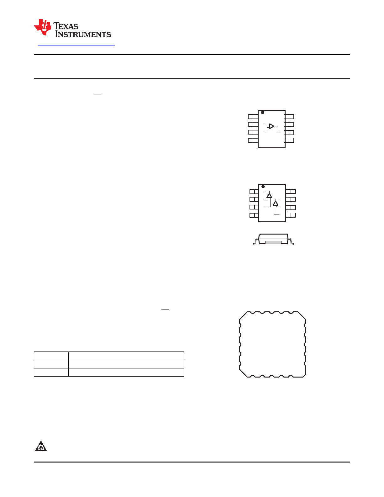
THS4032
D AND DGN PACKAGE
(TOP VIEW)
1
2
3
4
8
7
6
5
1OUT
1IN−
1IN+
−V
CC
V
CC+
2OUT
2IN−
2IN+
1
2
3
4
8
7
6
5
NULL
IN−
IN+
V
CC−
NULL
V
CC+
OUT
NC
THS4031
D, DGN, AND JG PACKAGE
(TOP VIEW)
NC − No internal connection
Cross-Section View Showing
PowerPAD Option (DGN)
192013 2
17
18
16
15
14
1312119 10
5
4
6
7
8
NC
V
CC+
NC
OUT
NC
NC
IN−
NC
IN+
NC
NC
NULLNCNULL
NC
V
NCNCNC
NC
THS4031
FK PACKAGE
(TOP VIEW)
CC−
查询"THS4031M"供应商
THS4031
THS4032
www.ti.com
1
FEATURES
2
• Ultralow 1.6 nV/√Hz Voltage Noise
• High Speed:
– 100-MHz Bandwidth [G = 2 (-1), –3 dB]
– 100-V/ms Slew Rate
• Very Low Distortion
– THD = –72 dBc (f = 1 MHz, RL= 150 Ω)
– THD = –90 dBc (f = 1 MHz, RL= 1 kΩ)
• Low 0.5-mV (Typ) Input Offset Voltage
• 90-mA Output Current Drive (Typical)
• ±5 V to ±15 V Typical Operation
• Available in Standard SOIC, MSOP
PowerPAD™, JG, or FK Package
• Evaluation Module Available
DESCRIPTION
The THS4031 and THS4032 are ultralow-voltage
noise, high-speed voltage feedback amplifiers that
are ideal for applications requiring low voltage noise,
including communications and imaging. The single
amplifier THS4031 and the dual amplifier THS4032
offer very good ac performance with 100-MHz
bandwidth (G = 2), 100-V/ms slew rate, and 60-ns
settling time (0.1%). The THS4031 and THS4032 are
unity gain stable with 275-MHz bandwidth. These
amplifiers have a high drive capability of 90 mA and
draw only 8.5-mA supply current per channel. With
–90 dBc of total harmonic distortion (THD) at f = 1
MHz and a very low noise of 1.6 nV/√Hz, the
THS4031 and THS4032 are ideally suited for
applications requiring low distortion and low noise
such as buffering analog-to-digital converters.
SLOS224G –JULY 1999–REVISED MARCH 2010
100-MHz LOW-NOISE HIGH-SPEED AMPLIFIERS
Check for Samples: THS4031, THS4032
DEVICE DESCRIPTION
THS4051/2 70-MHz High-Speed Amplifiers
THS4081/2 175-MHz Low Power High-Speed Amplifiers
space
1
2PowerPAD is a trademark of Texas Instruments.
PRODUCTION DATA information is current as of publication date.
Products conform to specifications per the terms of the Texas
Instruments standard warranty. Production processing does not
necessarily include testing of all parameters.
RELATED DEVICES
Copyright © 1999–2010, Texas Instruments Incorporated
Please be aware that an important notice concerning availability, standard warranty, and use in critical applications of Texas
Instruments semiconductor products and disclaimers thereto appears at the end of this data sheet.
V
n
I
n
1
10 100 1 k
− Voltage Noise −
10
f − Frequency − Hz
VOLTAGE NOISE AND CURRENT NOISE
vs
FREQUENCY
20
10 k 100 k
V
n
nV/ Hz
VCC = ± 15 V AND ± 5 V
TA = 25°C
− Current Noise −I
n
pA/ Hz
THS4031
THS4032
SLOS224G –JULY 1999–REVISED MARCH 2010
查询"THS4031M"供应商
These devices have limited built-in ESD protection. The leads should be shorted together or the device placed in conductive foam
during storage or handling to prevent electrostatic damage to the MOS gates.
www.ti.com
AVAILABLE OPTIONS
PACKAGED DEVICES
T
A
0°C to 70°C
–40°C to 85°C
–55°C to 125°C 1 — — — THS4031MJG THS4031MFK —
(1) For the most current package and ordering information, see the Package Option Addendum at the end of this document, or see the TI
web site at www.ti.com.
(2) The D and DGN packages are available taped and reeled. Add an R suffix to the device type (that is, THS4031CDGNR).
(3) The PowerPAD™ on the underside of the DGN package is electrically isolated from all other pins and active circuitry. Connection to the
PCB ground plane is recommended, although not required, as this copper plane is typically the largest copper plane on the PCB.
NUMBER OF EVALUATION
CHANNELS MODULE
1 THS4031CD THS4031CDGN TIACM — — THS4031EVM
2 THS4032CD THS4032CDGN TIABD — — THS4032EVM
1 THS4031ID THS4031IDGN TIACN — — —
2 THS4032ID THS4032IDGN TIABG — — —
PLASTIC PLASTIC MSOP
SMALL
OUTLINE
(2)
(D)
DEVICE SYMBOL
(2)
(DGN)
(1)
(3)
CERAMIC DIP CHIP CARRIER
(JG) (FK)
2 Submit Documentation Feedback Copyright © 1999–2010, Texas Instruments Incorporated
Product Folder Link(s): THS4031 THS4032
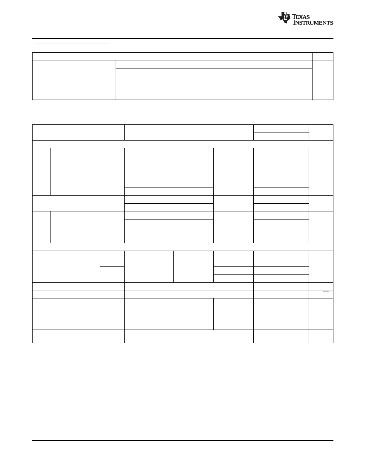
OUT
8
6
1
IN−
IN+
2
3
Null
−
+
1OUT
1IN−
1IN+
V
CC
2OUT
2IN−
2IN+
−V
CC
8
6
1
2
3
5
7
4
−
+
−
+
THS4031
THS4032
www.ti.com
查询"THS4031M"供应商
SLOS224G –JULY 1999–REVISED MARCH 2010
FUNCTIONAL BLOCK DIAGRAMS
Figure 1. THS4031 – Single Channel Figure 2. THS4032 – Dual Channel
CC–
(1)
VALUE UNIT
33 V
CC
(2)
130 °C
ABSOLUTE MAXIMUM RATINGS
Over operating free-air temperature range (unless otherwise noted).
V
CC
V
I
I
O
V
IO
T
A
T
J
T
stg
(1) Stresses beyond those listed under absolute maximum ratings may cause permanent damage to the device. These are stress ratings
only and functional operation of the device at these or any other conditions beyond those indicated under recommended operating
conditions is not implied. Exposure to absolute-maximum-rated conditions for extended periods may affect device reliability.
(2) The maximum junction temperature for continuous operation is limited by package constraints. Operation above this temperature may
result in reduced reliability and/or lifetime of the device. Does not apply to the JG package or FK package.
Supply voltage, V
CC+
to V
Input voltage ±V
Output current 150 mA
Differential input voltage ±4 V
Continuous total power dissipation See Dissipation Ratings Table
C-suffix 0 to 70
Operating free-air
temperature
I-suffix –40 to 85 °C
M-suffix –55 to 125
Maximum junction temperature, (any condition) 150 °C
Maximum junction temperature, continuous operation, long term reliability
Storage temperature –65 to 150 °C
Lead temperature 1,6 mm (1/16 inch) from case for 10 seconds 300 °C
Lead temperature 1,6 mm (1/16 inch) from case for 60 seconds, JG package 300 °C
Case temperature for 60 seconds, FK package 260 °C
DISSIPATION RATINGS TABLE
q
PACKAGE
D 167
(2)
DGN
(1) This data was taken using the JEDEC standard Low-K test PCB. For the JEDEC Proposed High-K test PCB, the qJAis 95°C/W with a
(2) This data was taken using 2 oz. trace and copper pad that is soldered directly to a 3-in. × 3-in. PC. For further information, refer to
Copyright © 1999–2010, Texas Instruments Incorporated Submit Documentation Feedback 3
JG 119 28 1050 mW, TJ= 150°C, continuous
FK 87.7 20 1375 mW, TJ= 150°C, continuous
power rating at TA= 25°C of 1.32 W.
Application Information section of this data sheet.
JA
(°C/W) (°C/W) POWER RATING
(1)
58.4 4.7 1.8 W, TJ= 130°C, continuous
q
JC
TA= 25°C,
38.3 629 mW, TJ= 130°C, continuous
Product Folder Link(s): THS4031 THS4032
THS4031
THS4032
SLOS224G –JULY 1999–REVISED MARCH 2010
查询"THS4031M"供应商
www.ti.com
RECOMMENDED OPERATING CONDITIONS
MIN NOM MAX UNIT
V
CC+
and V
Supply voltage V
CC–
Dual supply ±4.5 ±16
Single supply 9 32
C-suffix 0 70
T
A
Operating free-air
temperature
I-suffix –40 85 °C
M-suffix –55 125
ELECTRICAL CHARACTERISTICS
At TA= 25°C, VCC= ±15 V, and RL= 150 Ω (unless otherwise noted).
PARAMETER TEST CONDITIONS
(1)
DYNAMIC PERFORMANCE
Small-signal bandwidth (–3 dB) Gain = –1 or 2 MHz
BW Bandwidth for 0.1-dB flatness Gain = –1 or 2 MHz
Full power bandwidth
SR Slew rate
(3)
(2)
Settling time to 0.1% Gain = –1 ns
t
S
Settling time to 0.01% Gain = –1 ns
VCC= ±15 V 100
VCC= ±5 V 90
VCC= ±15 V 50
VCC= ±5 V 45
V
= 20 V, VCC= ±15 V 2.3
O(pp)
V
= 5 V, VCC= ±5 V 7.2
O(pp)
VCC= ±15 V, 20-V step 100
VCC= ±5 V, 5-V step 80
RL= 1 kΩ MHz
Gain = –1 V/ms
VCC= ±15 V, 5-V step 60
VCC= ±5 V, 2.5-V step 45
VCC= ±15 V, 5-V step 90
VCC= ±5 V, 2.5-V step 80
NOISE/DISTORTION PERFORMANCE
THD dBc
Total harmonic VCC= ±5 V or ±15 V, V
distortion f = 1 MHz Gain = 2
O(pp)
= 2 V,
THS4032
THS4031
V
I
Input voltage noise VCC= ±5 V or ±15 V, f > 10 kHz 1.6 nV/√Hz
n
Input current noise VCC= ±5 V or ±15 V, f > 10 kHz 1.2 pA/√Hz
n
Differential gain error
Gain = 2, NTSC and PAL,
40 IRE modulation, ±100 IRE ramp
Differential phase error °
Channel-to-channel crosstalk
(THS4032 only)
VCC= ±5 V or ±15 V, f = 1 MHz –61 dBc
RL= 150 Ω –81
RL= 1 kΩ –96
RL= 150 Ω –72
RL= 1 kΩ –90
VCC= ±15 V 0.015%
VCC= ±5 V 0.02%
VCC= ±15 V 0.025
VCC= ±5 V 0.03
(1) Full range = 0°C to 70°C for THS403xC and –40°C to 85°C for THS403xI suffix.
(2) Full power bandwidth = slew rate / [√2 pV
(3) Slew rate is measured from an output level range of 25% to 75%.
OC(Peak)
].
THS403xC, THS403xI
MIN TYP MAX
UNIT
4 Submit Documentation Feedback Copyright © 1999–2010, Texas Instruments Incorporated
Product Folder Link(s): THS4031 THS4032
THS4031
THS4032
www.ti.com
查询"THS4031M"供应商
SLOS224G –JULY 1999–REVISED MARCH 2010
ELECTRICAL CHARACTERISTICS (continued)
At TA= 25°C, VCC= ±15 V, and RL= 150 Ω (unless otherwise noted).
PARAMETER TEST CONDITIONS
(1)
DC PERFORMANCE
VCC= ±15 V, RL= 1 kΩ, VO= ±10 V
Open loop gain dB
VCC= ±5 V, RL= 1 kΩ, VO= ±2.5 V
V
I
I
Input offset voltage VCC= ±5 V or ±15 V mV
OS
Input bias current VCC= ±5 V or ±15 V mA
IB
Input offset current VCC= ±5 V or ±15 V nA
OS
TA= 25°C 93 98
TA= full range 92
TA= 25°C 90 95
TA= full range 89
TA= 25°C 0.5 2
TA= full range 3
TA= 25°C 3 6
TA= full range 8
TA= 25°C 30 250
TA= full range 400
Offset voltage drift VCC= ±5 V or ±15 V TA= full range 2 mV/°C
Input offset current drift VCC= ±5 V or ±15 V TA= full range 0.2 nA/°C
INPUT CHARACTERISTICS
V
Common-mode input voltage
ICR
range
CMRR Common-mode rejection ratio dB
r
C
Input resistance 2 MΩ
i
Input capacitance 1.5 pF
i
VCC= ±15 V ±13.5 ±14.0
VCC= ±5 V ±3.8 ±4.0
VCC= ±15 V, V
VCC= ±5 V, V
ICR
ICR
= ±12 V
= ±2.5 V
TA= 25°C 85 95
TA= full range 80
TA= 25°C 90 100
TA= full range 85
OUTPUT CHARACTERISTICS
VCC= ±15 V ±13 ±13.6
V
Output voltage swing V
O
VCC= ±5 V ±3.4 ±3.8
VCC= ±15 V RL= 150 Ω ±12 ±12.9
RL= 1 kΩ
VCC= ±5 V RL= 250 Ω ±3 ±3.5
I
I
R
Output current
O
Short-circuit current
SC
Output resistance Open loop 13 Ω
O
(4)
(4)
VCC= ±15 V 60 90
VCC= ±5 V 50 70
RL= 20 Ω mA
VCC= ±15 V 150 mA
POWER SUPPLY
V
I
Supply voltage operating range V
CC
Supply current (each amplifier) mA
CC
PSRR Power-supply rejection ratio VCC= ±5 V or ±15 V dB
Dual supply ±4.5 ±16.5
Single supply 9 33
VCC= ±15 V
VCC= ±5 V
TA= 25°C 8.5 10
TA= full range 11
TA= 25°C 7.5 9
TA= full range 10.5
TA= 25°C 85 95
TA= full range 80
(4) Observe power dissipation ratings to keep the junction temperature below the absolute maximum rating when the output is heavily
loaded or shorted. See the Absolute Maximum Ratings table in this data sheet for more information.
THS403xC, THS403xI
MIN TYP MAX
UNIT
V
Copyright © 1999–2010, Texas Instruments Incorporated Submit Documentation Feedback 5
Product Folder Link(s): THS4031 THS4032
THS4031
THS4032
SLOS224G –JULY 1999–REVISED MARCH 2010
查询"THS4031M"供应商
www.ti.com
ELECTRICAL CHARACTERISTICS
At TA= full range, VCC= ±15 V, and RL= 1 kΩ (unless otherwise noted).
PARAMETER TEST CONDITIONS
(1)
DYNAMIC PERFORMANCE
Unity gain bandwidth VCC= ±15 V, Closed loop RL= 1 kΩ 100
Small-signal bandwidth (–3 dB) Gain = –1 or 2 MHz
BW VCC= ±15 V 50
Bandwidth for 0.1-dB flatness Gain = –1 or 2 MHz
Full power bandwidth
(3)
VCC= ±15 V 100
VCC= ±5 V 90
VCC= ±5 V 45
V
= 20 V, VCC= ±15 V 2.3
O(pp)
V
= 5 V, VCC= ±5 V 7.1
O(pp)
RL= 1 kΩ MHz
SR Slew rate VCC= ±15 V RL= 1 kΩ 80
Settling time to 0.1% Gain = –1 ns
t
S
Settling time to 0.01% Gain = –1 ns
VCC= ±15 V, 5-V step 60
VCC= ±5 V, 2.5-V step 45
VCC= ±15 V, 5-V step 90
VCC= ±5 V, 2.5-V step 80
NOISE/DISTORTION PERFORMANCE
THD Total harmonic distortion dBc
V
I
Input voltage noise f > 10 kHz RL= 150 Ω 1.6 nV/√Hz
n
Input current noise f > 10 kHz RL= 150 Ω 1.2 pA/√Hz
n
Differential gain error
VCC= ±5 V or ±15 V, V
f = 1 MHz, Gain = 2, TA= 25°C
VCC= ±5 V or ±15 V,
TA= 25°C
VCC= ±5 V or ±15 V,
TA= 25°C
Gain = 2, NTSC and PAL,
O(pp)
= 2 V,
40 IRE modulation, ±100 IRE ramp,
Differential phase error °
TA= 25°C RL= 150 Ω
RL= 150 Ω –81
RL= 1 kΩ –96
VCC= ±15 V 0.015%
VCC= ±5 V 0.02%
VCC= ±15 V 0.025
VCC= ±5 V 0.03
DC PERFORMANCE
VCC= ±15 V, RL= 1 kΩ, VO= ±10 V
Open loop gain dB
VCC= ±5 V, RL= 1 kΩ, VO= ±2.5 V
V
I
I
Input offset voltage VCC= ±5 V or ±15 V mV
OS
Input bias current VCC= ±5 V or ±15 V mA
IB
Input offset current VCC= ±5 V or ±15 V nA
OS
TA= 25°C 93 98
TA= full range 92
TA= 25°C 92 95
TA= full range 91
TA= 25°C 0.5 2
TA= full range 3
TA= 25°C 3 6
TA= full range 8
TA= 25°C 30 250
TA= full range 400
Offset voltage drift VCC= ±5 V or ±15 V TA= full range 2 mV/°C
Input offset current drift VCC= ±5 V or ±15 V TA= full range 0.2 nA/°C
(1) Full range = 0°C to 70°C for THS403xC and –40°C to 85°C for THS403xI suffix.
(2) This parameter is not tested.
(3) Full power bandwidth = slew rate / [√2 pV
OC(Peak)
].
THS403xC, THS403xI
MIN TYP MAX
(2)
120 MHz
(2)
100 V/ms
UNIT
6 Submit Documentation Feedback Copyright © 1999–2010, Texas Instruments Incorporated
Product Folder Link(s): THS4031 THS4032
THS4031
THS4032
www.ti.com
查询"THS4031M"供应商
SLOS224G –JULY 1999–REVISED MARCH 2010
ELECTRICAL CHARACTERISTICS (continued)
At TA= full range, VCC= ±15 V, and RL= 1 kΩ (unless otherwise noted).
PARAMETER TEST CONDITIONS
(1)
INPUT CHARACTERISTICS
V
Common-mode input voltage
ICR
range
CMRR Common-mode rejection ratio dB
r
C
Input resistance 2 MΩ
i
Input capacitance 1.5 pF
i
VCC= ±15 V ±13.5 ±14.3
VCC= ±5 V ±3.8 ±4.3
VCC= ±15 V, V
VCC= ±5 V, V
ICR
ICR
= ±12 V
= ±2.5 V
TA= 25°C 85 95
TA= full range 80
TA= 25°C 90 100
TA= full range 85
OUTPUT CHARACTERISTICS
VCC= ±15 V ±13 ±13.6
V
Output voltage swing V
O
VCC= ±5 V ±3.4 ±3.8
VCC= ±15 V RL= 150 Ω ±12 ±12.9
RL= 1 kΩ
VCC= ±5 V RL= 250 Ω ±3 ±3.5
I
I
R
Output current
O
Short-circuit current
SC
Output resistance Open loop 13 Ω
O
(4)
(4)
VCC= ±15 V 60 90
VCC= ±5 V 50 70
RL= 20 Ω mA
VCC= ±15 V 150 mA
POWER SUPPLY
V
I
Supply voltage operating range V
CC
Supply current (each amplifier) mA
CC
PSRR Power-supply rejection ratio VCC= ±5 V or ±15 V dB
Dual supply ±4.5 ±16.5
Single supply 9 33
VCC= ±15 V
VCC= ±5 V
TA= 25°C 8.5 10
TA= full range 11
TA= 25°C 7.5 9
TA= full range 10
TA= 25°C 85 95
TA= full range 80
(4) Observe power dissipation ratings to keep the junction temperature below the absolute maximum rating when the output is heavily
loaded or shorted. See the Absolute Maximum Ratings table in this data sheet for more information.
THS403xC, THS403xI
MIN TYP MAX
UNIT
V
Copyright © 1999–2010, Texas Instruments Incorporated Submit Documentation Feedback 7
Product Folder Link(s): THS4031 THS4032
_
+
330 Ω
50 Ω
150 Ω
V
O1
V
I1
330 Ω
CH1
_
+
330 Ω
50 Ω
150 Ω
V
O2
V
I2
330 Ω
CH2
_
+
R
g
R
f
50 Ω
R
L
V
O
V
I
_
+
R
g
R
f
50 Ω
R
L
V
O
V
I
THS4031
THS4032
SLOS224G –JULY 1999–REVISED MARCH 2010
查询"THS4031M"供应商
PARAMETER MEASUREMENT INFORMATION
Figure 4. Step Response Test Circuit Figure 5. Step Response Test Circuit
www.ti.com
Figure 3. THS4032 Crosstalk Test Circuit
Product Folder Link(s): THS4031 THS4032
8 Submit Documentation Feedback Copyright © 1999–2010, Texas Instruments Incorporated
THS4031
THS4032
www.ti.com
查询"THS4031M"供应商
SLOS224G –JULY 1999–REVISED MARCH 2010
TYPICAL CHARACTERISTICS
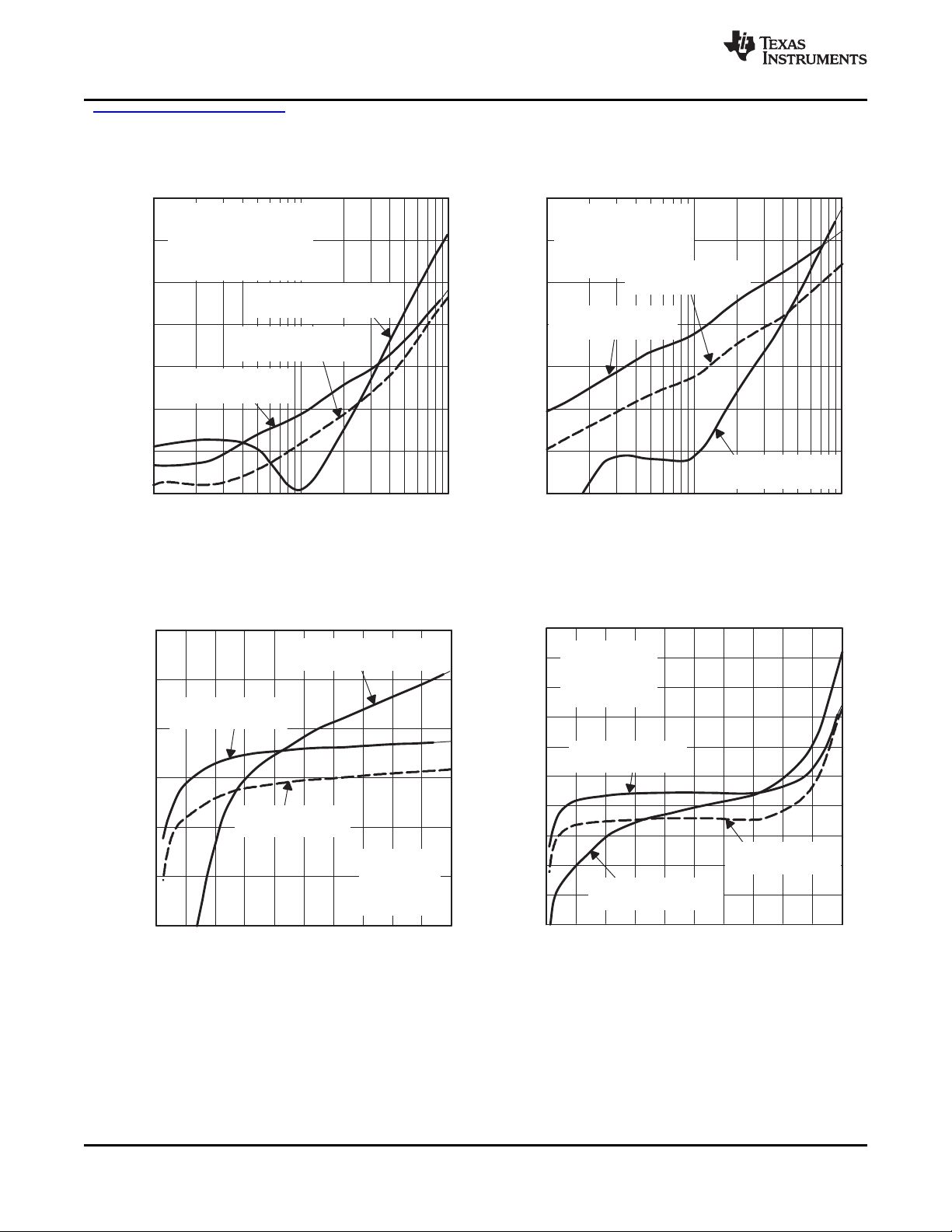
Table of Graphs
FIGURE
Input offset voltage distribution 6, 7
Input offset voltage vs Free-air temperature 8
Input bias current vs Free-air temperature 9
Output voltage swing vs Supply voltage 10
Maximum output voltage swing vs Free-air temperature 11
Maximum output current vs Free-air temperature 12
Supply current vs Free-air temperature 13
Common-mode input voltage vs Supply voltage 14
Closed-loop output impedance vs Frequency 15
Open-loop gain and phase response vs Frequency 16
Power-supply rejection ratio vs Frequency 17
Common-mode rejection ratio vs Frequency 18
Crosstalk vs Frequency 19
Harmonic distortion vs Frequency 20, 21
Harmonic distortion vs Peak-to-peak output voltage 22, 23
Slew rate vs Free-air temperature 24
0.1% settling time vs Output voltage step size 25
Small signal frequency response with varying feedback resistance Gain = 1, VCC= ±15V, RL= 1kΩ 26
Frequency response with varying output voltage swing Gain = 1, VCC= ±15V, RL= 1kΩ 27
Small signal frequency response with varying feedback resistance Gain = 1, VCC= ±15V, RL= 150kΩ 28
Frequency response with varying output voltage swing Gain = 1, VCC= ±15V, RL= 150kΩ 29
Small signal frequency response with varying feedback resistance Gain = 1, VCC= ±5V, RL= 1kΩ 30
Frequency response with varying output voltage swing Gain = 1, VCC= ±5V, RL= 1kΩ 31
Small signal frequency response with varying feedback resistance Gain = 1, VCC= ±5V, RL= 150kΩ 32
Frequency response with varying output voltage swing Gain = 1, VCC= ±5V, RL= 150kΩ 33
Small signal frequency response with varying feedback resistance Gain = 2, VCC= ±5V, RL= 150kΩ 34
Small signal frequency response with varying feedback resistance Gain = 2, VCC= ±5V, RL= 150kΩ 35
Small signal frequency response with varying feedback resistance Gain = –1, VCC= ±15V, RL= 150kΩ 36
Frequency response with varying output voltage swing Gain = –1, VCC= ±5V, RL= 150kΩ 37
Small signal frequency response Gain = 5, VCC= ±15V, ±5V 38
Output amplitude vs Frequency, Gain = 2, VS= ±15V 39
Output amplitude vs Frequency, Gain = 2, VS= ±5V 40
Output amplitude vs Frequency, Gain = –1, VS= ±15V 41
Output amplitude vs Frequency, Gain = –1, VS= ±5V 42
Differential phase vs Number of 150Ω loads 43, 44
Differential gain vs Number of 150Ω loads 45, 46
1-V step response vs Time 47, 48
4-V step response vs Time 49
20-V step response vs Time 50
Copyright © 1999–2010, Texas Instruments Incorporated Submit Documentation Feedback 9
Product Folder Link(s): THS4031 THS4032
8
6
4
0
−2 −1.6 −1.2 −0.8 −0.4 0
Percentage of Amplifiers − %
10
12
14
0.4 0.8 1.2
2
VIO − Input Offset Voltage − mV
VCC = ± 15 V
250 Samples
3 Wafer Lots
TA = 25°C
15
12.5
7.5
0
−2 −1.6 −1.2 −0.8 −0.4 0
Percentage of Amplifiers − %
17.5
20
22.5
0.4 0.8 1.2
2.5
VIO − Input Offset Voltage − mV
VCC = ± 5 V
250 Samples
3 Wafer Lots
TA = 25°C
10
5
2.90
2.85
2.80
2.70
−40 −20 0 20 40
− Input Bias Current −
3
3.05
3.10
60 80 100
2.95
2.75
TA − Free-Air Temperature − °C
I
IB
VCC = ± 15 V
VCC = ± 5 V
Aµ
VCC = ± 5 V
VCC = ± 15 V
−0.45
−0.5
−0.55
−0.6
−40 −20 0 20
− Input Offset Voltage − mV
−0.4
−0.35
−0.3
40 100
60
80
TA − Free-Air Temperature − °C
V
IO
THS4031
THS4032
SLOS224G –JULY 1999–REVISED MARCH 2010
查询"THS4031M"供应商
INPUT OFFSET VOLTAGE DISTRIBUTION INPUT OFFSET VOLTAGE DISTRIBUTION
Figure 6. Figure 7.
www.ti.com
TYPICAL CHARACTERISTICS
10 Submit Documentation Feedback Copyright © 1999–2010, Texas Instruments Incorporated
INPUT OFFSET VOLTAGE INPUT BIAS CURRENT
FREE-AIR TEMPERATURE FREE-AIR TEMPERATURE
vs vs
Figure 8. Figure 9.
Product Folder Link(s): THS4031 THS4032
RL=1KΩ
RL=150 Ω
TA=25°C
8
6
4
2
5 7 9 11
– OutputV
oltageSwing –
10
12
14
13 15
± VCC– SupplyVoltage –± V
V
O
|
|
± V
12
4.5
3.5
2.5
−40 −20 0 20 40
− Maximum Output Voltage Swing −
13
13.5
14
60 80 100
12.5
4
3
VCC = ± 5 V
RL = 150 Ω
VCC = ± 5 V
RL = 1 kΩ
TA − Free-Air Temperature − °C
VCC = ± 15 V
RL = 1 kΩ
VCC = ± 15 V
RL = 250 Ω
±VV
OM
80
70
60
50
−40 −20 0 20 40
− Maximum Output Current − mA
90
100
110
60 80 100
TA − Free-Air Temperature − °C
I
O
VCC = ± 15 V
Source Current
VCC = ± 15 V
Sink Current
VCC = ± 5 V
Sink Current
VCC = ± 5 V
Source Current
RL = 20 Ω
8
7
6
5
−40 −20 0 20
40
− Supply Current − mA
9
10
11
60 80 100
TA − Free-Air Temperature − °C
I
CC
VCC = ± 15 V
VCC = ± 5 V
VCC = ± 10 V
Each Amplifier
THS4031
THS4032
www.ti.com
查询"THS4031M"供应商
OUTPUT VOLTAGE SWING MAXIMUM OUTPUT VOLTAGE SWING
SUPPLY VOLTAGE FREE-AIR TEMPERATURE
Figure 10. Figure 11.
SLOS224G –JULY 1999–REVISED MARCH 2010
TYPICAL CHARACTERISTICS (continued)
vs vs
Copyright © 1999–2010, Texas Instruments Incorporated Submit Documentation Feedback 11
MAXIMUM OUTPUT CURRENT SUPPLY CURRENT
FREE-AIR TEMPERATURE FREE-AIR TEMPERATURE
vs vs
Figure 12. Figure 13.
Product Folder Link(s): THS4031 THS4032
9
7
5
3
5 7 9 11
− Common-Mode Input −
11
13
15
13 15
V
IC
±V
± VCC − Supply Voltage − ± V
TA = 25°C
1
0.1
0.01
100 k 1 M
− Closed-Loop Output Impedance −
10
f − Frequency − Hz
100
100 M 500 M
10 M
Z
O
Ω
Gain = 1
RF = 1 kΩ
PI = + 3 dBm
V
O
+
−
50 Ω
1 kΩ
1 kΩ
V
I
THS403x
(
V
O
V
I
=
1000
Z
o
)
− 1
40
20
0
−20
100 1 k 10 k 100 k 1 M
Open-Loop Gain − dB
60
80
f − Frequency − Hz
100
10 M 100 M 1 G
Gain
Phase
VCC = ± 15 V
RL = 150 Ω
Phase Response
0°
−45°
−90°
45°
−135°
−180°
−225°
THS4031
THS4032
SLOS224G –JULY 1999–REVISED MARCH 2010
查询"THS4031M"供应商
TYPICAL CHARACTERISTICS (continued)
COMMON-MODE INPUT VOLTAGE CLOSED-LOOP OUTPUT IMPEDANCE
SUPPLY VOLTAGE FREQUENCY
vs vs
www.ti.com
Figure 14. Figure 15.
OPEN-LOOP GAIN AND PHASE RESPONSE
Figure 16.
12 Submit Documentation Feedback Copyright © 1999–2010, Texas Instruments Incorporated
Product Folder Link(s): THS4031 THS4032
THS4032 − V
CC+
THS4031 − V
CC+
THS4031 − V
CC−
THS4032 − V
CC−
VCC = ± 15 V and ± 5 V
60
40
20
0
10 100 1 k 10 k 100 k
PSRR − Power-Supply Rejection Ratio − dB
80
100
f − Frequency − Hz
120
1 M 10 M 100 M
_
+
1 kΩ
1 kΩ
1 kΩ
1 kΩ
R
L
150 Ω
V
O
V
I
60
40
20
0
10 100 1 k 10 k 100 k
CMRR − Common-Mode Rejection Ratio − dB
80
100
f − Frequency − Hz
120
1 M 10 M 100 M
VCC = ± 15 V
VCC = ± 5 V
Input = CH 2
Output = CH 1
Input = CH 1
Output = CH 2
VCC = ± 15 V
PI = 0 dBm
See Figure 3
−30
−60
−70
−90
100 k 1 M 10 M
Crosstalk − dB
−20
−10
f − Frequency − Hz
0
100 M 500 M
−40
−50
−80
THS4031
THS4032
www.ti.com
查询"THS4031M"供应商
POWER-SUPPLY REJECTION RATIO COMMON-MODE REJECTION RATIO
FREQUENCY FREQUENCY
SLOS224G –JULY 1999–REVISED MARCH 2010
TYPICAL CHARACTERISTICS (continued)
vs vs
Figure 17. Figure 18.
THS4032
CROSSTALK
vs
FREQUENCY
Figure 19.
Copyright © 1999–2010, Texas Instruments Incorporated Submit Documentation Feedback 13
Product Folder Link(s): THS4031 THS4032
−70
−80
−100
−110
100 k 1 M
Harmonic Distortion − dBc
−60
−50
f − Frequency − Hz
−40
10 M
−90
THS4031
Second Harmonic
THS4032
Second Harmonic
VCC = ± 15 V and ± 5 V
Gain = 2
RF = 300 Ω
RL = 1 kΩ
V
O(PP)
= 2 V
THS4031 and THS4032
Third Harmonics
−70
−80
−100
−110
100 k 1 M
Harmonic Distortion − dBc
−60
−50
f − Frequency − Hz
−40
10 M
−90
THS4032
Second Harmonic
VCC = ± 15 V and ± 5 V
Gain = 2
RF = 300 Ω
R
L
= 150 Ω
V
O(PP)
= 2 V
THS4031 and THS4032
Third Harmonics
THS4031
Second Harmonic
THS4032
Second Harmonic
VCC = ± 15 V
Gain = 5
RF = 300 Ω
R
L
= 1 kΩ
f = 1 MHz
THS4031 and THS4032
Third Harmonics
THS4031
Second Harmonic
−80
−90
−100
−110
0 2 4 6 8 10 12
Harmonic Distortion − dBc
−70
−60
−50
14 16 18 20
V
O(PP)
− Peak-to-Peak Output Voltage − V
THS4032
Second Harmonic
VCC = ± 15 V
Gain = 5
RF = 300 Ω
RL = 150 Ω
f = 1 MHz
THS4031 and THS4032
Third Harmonics
THS4031
Second Harmonic
−80
−90
−100
−110
0 2 4 6 8 10 12
Harmonic Distortion − dBc
−70
−60
−50
14 16 18 20
V
O(PP)
− Peak-to-Peak Output Voltage − V
−40
−30
−20
−10
THS4031
THS4032
SLOS224G –JULY 1999–REVISED MARCH 2010
查询"THS4031M"供应商
TYPICAL CHARACTERISTICS (continued)
HARMONIC DISTORTION HARMONIC DISTORTION
vs vs
FREQUENCY FREQUENCY
www.ti.com
14 Submit Documentation Feedback Copyright © 1999–2010, Texas Instruments Incorporated
Figure 20. Figure 21.
HARMONIC DISTORTION HARMONIC DISTORTION
vs vs
PEAK-TO-PEAK OUTPUT VOLTAGE PEAK-TO-PEAK OUTPUT VOLTAGE
Figure 22. Figure 23.
Product Folder Link(s): THS4031 THS4032

40
30
20
0
1 2 3
− 0.1% Settling Time − ns
60
70
80
4 5
50
10
VO − Output Voltage Step Size − V
t
s
VCC = ± 5 V
VCC = ± 15 V
Gain = −1
RF = 430 Ω
90
80
60
50
−40 −20 0 20 40
SR − Slew Rate −
100
110
120
60 80 100
70
sµ
V/
TA − Free-Air Temperature − °C
Gain = −1
RL = 150 Ω
Vcc = ± 15 V
Step = 20 V
Vcc = ± 5 V
Step = 4 V
−6
−5
−4
−3
−2
−1
0
1
2
3
100 k 1 M 10 M 100 M 500 M
VO = 0.1 V
(PP)
VO = 0.2 V
(PP)
VO = 0.4 V
(PP)
VO = 0.8 V
(PP)
VO = 1.6 V
(PP)
VCC = +15 V,
RL = 1 kW,
Gain = 1,
RF = 0 W
f − Frequency − Hz
Output Amplitude (Large Signal) − dB
−7
−6
−5
−4
−3
−2
−1
0
1
2
100k 1M 10M 100M 500M
Output
Amplitude − dB
f − Frequency − Hz
R =200FW
R =50FW
R =100FW
R =0FW
V = 15V,
R =150 ,
V =200mV,
Gain=1
CC
L
O(PP)
±
W
THS4031
THS4032
www.ti.com
查询"THS4031M"供应商
SLEW RATE 0.1% SETTLING TIME
FREE-AIR TEMPERATURE OUTPUT VOLTAGE STEP SIZE
SLOS224G –JULY 1999–REVISED MARCH 2010
TYPICAL CHARACTERISTICS (continued)
vs vs
Figure 24. Figure 25.
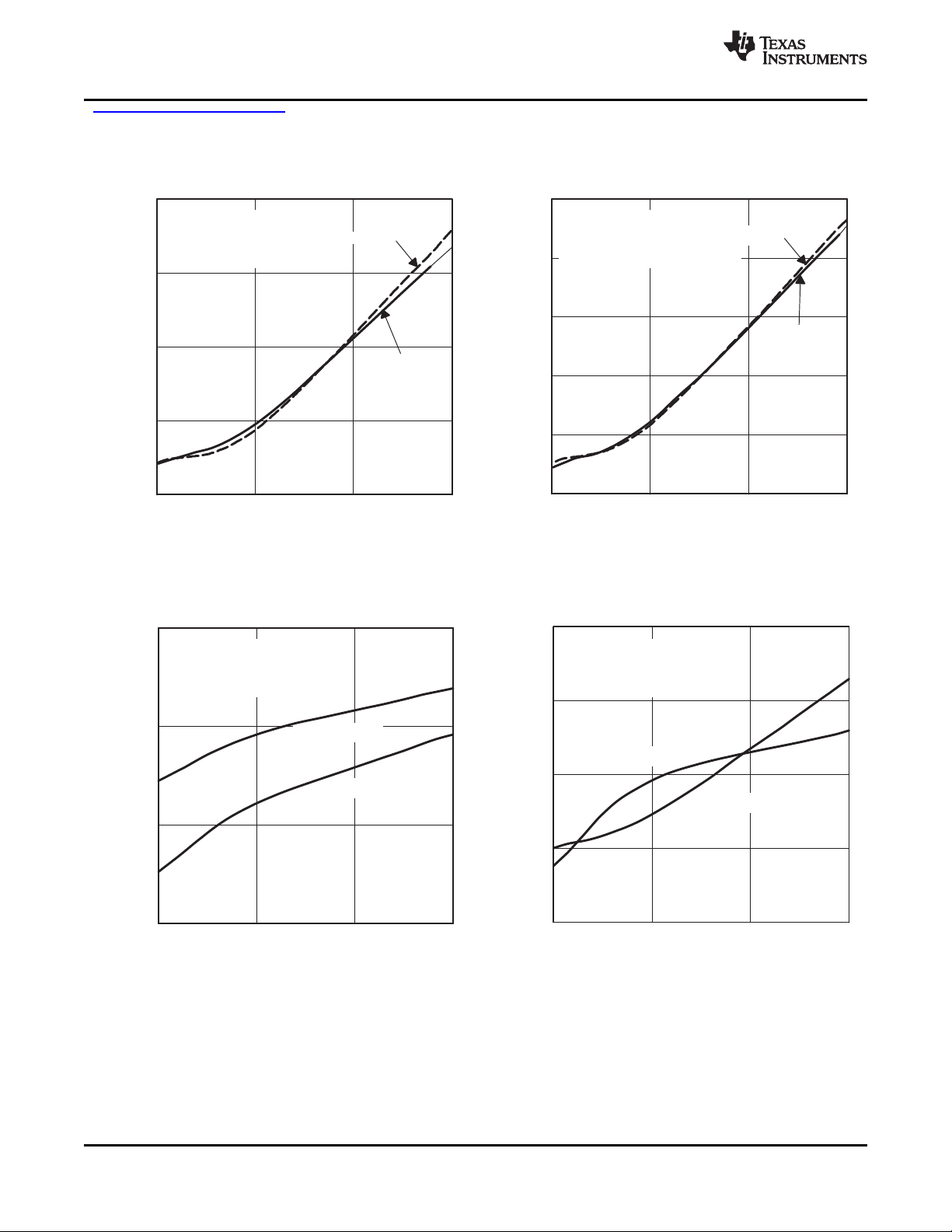
SMALL SIGNAL FREQUENCY RESPONSE FREQUENCY RESPONSE WITH
WITH VARYING FEEDBACK RESISTANCE VARYING OUTPUT VOLTAGE SWING
Figure 26. Figure 27.
Copyright © 1999–2010, Texas Instruments Incorporated Submit Documentation Feedback 15
Product Folder Link(s): THS4031 THS4032

−6
−5
−4
−3
−2
−1
0
1
2
3
100 k 1 M 10 M 100 M 500 M
VO = 0.1 V
(PP)
Output Amplitude (Large Signal) − dB
VCC = +15 V,
RL = 150 W,
Gain = 1,
RF = 0 W
f − Frequency − Hz
VO = 0.2 V
(PP)
VO = 0.4 V
(PP)
VO = 0.8 V
(PP)
VO = 1.6 V
(PP)
−7
−6
−5
−4
−3
−2
−1
0
1
2
100k 1M 10M 100M 500M
Output
Amplitude − dB
f − Frequency − Hz
R =200FW
R =50FW
R =100FW
R =0FW
V = 15V,
R =150 ,
V =200mV,
Gain=1
CC
L
O(PP)
±
W
V = 5V,
R =1k ,
V =200mV
Gain=1
CC
L
O(PP)
±
W
R =200FW
R =100FW
R =50FW
R =0FW
−6
−5
−4
−3
−2
−1
0
1
2
3
100 k 1 M 10 M 100 M 500 M
VO = 0.1 V
(PP)
VCC = 5 V,
RL = 1 kW,
Gain = 1,
RF = 0 W
f − Frequency − Hz
VO = 0.2 V
(PP)
VO = 0.4 V
(PP)
VO = 0.8 V
(PP)
VO = 1.6 V
(PP)
Output Amplitude (Large Signal) − dB
THS4031
THS4032
SLOS224G –JULY 1999–REVISED MARCH 2010
查询"THS4031M"供应商
TYPICAL CHARACTERISTICS (continued)
SMALL SIGNAL FREQUENCY RESPONSE FREQUENCY RESPONSE WITH
WITH VARYING FEEDBACK RESISTANCE VARYING OUTPUT VOLTAGE SWING
Figure 28. Figure 29.
www.ti.com
SMALL SIGNAL FREQUENCY RESPONSE FREQUENCY RESPONSE WITH
WITH VARYING FEEDBACK RESISTANCE VARYING OUTPUT VOLTAGE SWING
16 Submit Documentation Feedback Copyright © 1999–2010, Texas Instruments Incorporated
Figure 30. Figure 31.
Product Folder Link(s): THS4031 THS4032

V = 5V,
R =150 ,
V =200mV
Gain=1
CC
L
O(PP)
±
W
R =200FW
R =100FW
R =50FW
R =0FW
−6
−5
−4
−3
−2
−1
0
1
2
3
100 k 1 M 10 M 100 M 500 M
VO = 0.1 V
(PP)
VCC = 5 V,
RL = 150 W,
Gain = 1,
RF = 0 W
f − Frequency − Hz
VO = 0.2 V
(PP)
VO = 0.4 V
(PP)
VO = 0.8 V
(PP)
VO = 1.6 V
(PP)
Output Amplitude (Large Signal) − dB
R =300FW
R =1kFW
R =100FW
V = 15V
Gain=2
R =150
V =0.4V
CC
L
O(PP)
±
W
3
2
1
−1
100 k 1 M 10 M
Output Amplitude − dB
5
7
f − Frequency − Hz
8
100 M 500 M
6
4
0
VCC = ± 5 V
Gain = 2
RL = 150 Ω
V
O(PP)
= 0.4 V
RF = 1 kΩ
RF = 300 Ω
RF = 100 Ω
THS4031
THS4032
www.ti.com
查询"THS4031M"供应商
SMALL SIGNAL FREQUENCY RESPONSE FREQUENCY RESPONSE WITH
WITH VARYING FEEDBACK RESISTANCE VARYING OUTPUT VOLTAGE SWING
Figure 32. Figure 33.
SLOS224G –JULY 1999–REVISED MARCH 2010
TYPICAL CHARACTERISTICS (continued)
SMALL SIGNAL FREQUENCY RESPONSE SMALL SIGNAL FREQUENCY RESPONSE
WITH VARYING FEEDBACK RESISTANCE WITH VARYING FEEDBACK RESISTANCE
Copyright © 1999–2010, Texas Instruments Incorporated Submit Documentation Feedback 17
Figure 34. Figure 35.
Product Folder Link(s): THS4031 THS4032

−3
−4
−5
−7
100 k 1 M 10 M
Output Amplitude − dB
−1
1
f − Frequency − Hz
2
100 M 500 M
0
−2
−6
VCC = ± 15 V
Gain = −1
RL = 150 Ω
V
O(PP)
= 0.4 V
RF = 1 kΩ
RF = 360 Ω
RF = 100 Ω
−3
−4
−5
−7
100 k 1 M 10 M
Output Amplitude − dB
−1
1
f − Frequency − Hz
2
100 M 500 M
0
−2
−6
VCC = ± 5 V
Gain = −1
RL = 150 Ω
V
O(PP)
= 0.4 V
RF = 1 kΩ
RF = 360 Ω
RF = 100 Ω
10
6
4
0
100 k 1 M 10 M
Output Amplitude − dB
12
14
f − Frequency − Hz
16
100 M 500 M
8
2
VCC = ± 15 V
VCC = ± 5 V
Gain = 5
RF = 3.9 kΩ
RL = 150 Ω
V
O(PP)
= 0.4 V
THS4031
THS4032
SLOS224G –JULY 1999–REVISED MARCH 2010
查询"THS4031M"供应商
TYPICAL CHARACTERISTICS (continued)
SMALL SIGNAL FREQUENCY RESPONSE SMALL SIGNAL FREQUENCY RESPONSE
WITH VARYING FEEDBACK RESISTANCE WITH VARYING FEEDBACK RESISTANCE
Figure 36. Figure 37.
www.ti.com
18 Submit Documentation Feedback Copyright © 1999–2010, Texas Instruments Incorporated
SMALL SIGNAL
FREQUENCY RESPONSE
Figure 38.
Product Folder Link(s): THS4031 THS4032
−12
−15
−18
−24
100 k 1 M 10 M
− Output Voltage Level − dBV
−6
0
f − Frequency − Hz
3
100 M 500 M
−3
−9
−21
VCC = ± 15 V
Gain = 2
RF = 300 Ω
RL= 150 Ω
VI = 0.5 V RMS
VI = 0.25 V RMS
VI = 125 mV RMS
VI = 62.5 mV RMS
V
O
−24
−21
−18
−15
−12
−9
−6
−3
0
3
100k 1M 10M 100M 500M
f − Frequency − Hz
V OutputVoltageLevel dBv
O
− −
VCC= 5 V
Gain=2
RF=300 W
RL=150 W
V 0.25VRMS
I
=
V 125mVRMS
I
=
V 62.5mVRMS
I
=
V 0.5VRMS
I
=
18
−21
−24
−30
100 k 1 M 10 M
− Output Voltage Level − dBV
−12
−6
f − Frequency − Hz
−3
100 M 500 M
−9
−15
−27
VCC = ± 15 V
Gain = −1
RF = 430 Ω
RL = 150 Ω
VI = 0.5 V RMS
VI = 0.25 V RMS
VI = 125 mV RMS
VI = 62.5 mV RMS
V
O
18
−21
−24
−30
100 k 1 M 10 M
− Output Voltage Level − dBV
−12
−6
f − Frequency − Hz
−3
100 M 500 M
−9
−15
−27
VCC = ± 5 V
Gain = −1
RF = 430 Ω
RL = 150 Ω
VI = 0.5 V RMS
VI = 0.25 V RMS
VI = 125 mV RMS
VI = 62.5 mV RMS
V
O
THS4031
THS4032
www.ti.com
查询"THS4031M"供应商
OUTPUT AMPLITUDE OUTPUT AMPLITUDE
FREQUENCY FREQUENCY
SLOS224G –JULY 1999–REVISED MARCH 2010
TYPICAL CHARACTERISTICS (continued)
vs vs
Figure 39. Figure 40.
OUTPUT AMPLITUDE OUTPUT AMPLITUDE
vs vs
FREQUENCY FREQUENCY
Figure 41. Figure 42.
Copyright © 1999–2010, Texas Instruments Incorporated Submit Documentation Feedback 19
Product Folder Link(s): THS4031 THS4032
VCC = ± 5 V
1 2
Differential Phase
3 4
Gain = 2
RF = 680 Ω
40 IRE-NTSC Modulation
Worst Case ± 100 IRE Ramp
VCC = ± 15 V
0.2°
0.15°
0.1°
0.05°
0°
Number of 150-Ω Loads
VCC = ± 5 V
1 2
Differential Phase
3 4
Gain = 2
RF = 680 Ω
40 IRE-PAL Modulation
Worst Case ± 100 IRE Ramp
VCC = ± 15 V
0.25°
0.2°
0.15°
0.1°
0.05°
0°
Number of 150-Ω Loads
VCC = ± 5 V
1 2
Differential Gain − %
3 4
Gain = 2
RF = 680 Ω
40 IRE-NTSC Modulation
Worst Case ± 100 IRE Ramp
VCC = ± 15 V
0.025°
0.02°
0.015°
0.01°
Number of 150-Ω Loads
VCC = ± 5 V
1 2
Differential Gain − %
3 4
Gain = 2
RF = 680 Ω
40 IRE-PAL Modulation
Worst Case ± 100 IRE Ramp
VCC = ± 15 V
0.03
0.025
0.02
0.15
0.01
Number of 150-Ω Loads
THS4031
THS4032
SLOS224G –JULY 1999–REVISED MARCH 2010
查询"THS4031M"供应商
TYPICAL CHARACTERISTICS (continued)
DIFFERENTIAL PHASE DIFFERENTIAL PHASE
NUMBER OF 150-Ω LOADS NUMBER OF 150-Ω LOADS
vs vs
Figure 43. Figure 44.
www.ti.com
20 Submit Documentation Feedback Copyright © 1999–2010, Texas Instruments Incorporated
DIFFERENTIAL GAIN DIFFERENTIAL GAIN
NUMBER OF 150-Ω LOADS NUMBER OF 150-Ω LOADS
vs vs
Figure 45. Figure 46.
Product Folder Link(s): THS4031 THS4032

0
−0.2
−0.4
−0.6
− OutputV
oltage − V
0.2
0.4
0.6
V
O
VCC= ± 15V
Gain=2
RF=300 Ω
RL=150 Ω
SeeFigure4
t-Time-200ns/div
0
−0.2
−0.4
−0.6
− OutputV
oltage − V
0.2
0.4
0.6
V
O
VCC= ± 5V
Gain=2
RF=300 Ω
RL=150 Ω
SeeFigure4
t-Time-200ns/div
0
−0.5
−1.5
−2.5
− OutputV
oltage − V
1.5
2
2.5
V
O
VCC= ± 5V
Gain= −1
RF=430 Ω
RL=150 Ω
SeeFigure5
1
0.5
−1
−2
t-Time-200ns/div
0
−5
−10
−15
− OutputV
oltage − V
5
10
15
V
O
RL=1kΩ
RL=150 Ω
VCC= ± 15V
Gain=2
RF=330 Ω
SeeFigure4
OffsetForClarity
t-Time-200ns/div
THS4031
THS4032
www.ti.com
查询"THS4031M"供应商
1-V STEP RESPONSE 1-V STEP RESPONSE
Figure 47. Figure 48.
4-V STEP RESPONSE 20-V STEP RESPONSE
SLOS224G –JULY 1999–REVISED MARCH 2010
TYPICAL CHARACTERISTICS (continued)
Figure 49. Figure 50.
Copyright © 1999–2010, Texas Instruments Incorporated Submit Documentation Feedback 21
Product Folder Link(s): THS4031 THS4032
IN− (2)
IN+ (3)
NULL (1) NULL (8)
(6) OUT
(4) VCC−
(7) VCC+
THS4031
THS4032
SLOS224G –JULY 1999–REVISED MARCH 2010
查询"THS4031M"供应商
www.ti.com
APPLICATION INFORMATION
THEORY OF OPERATION
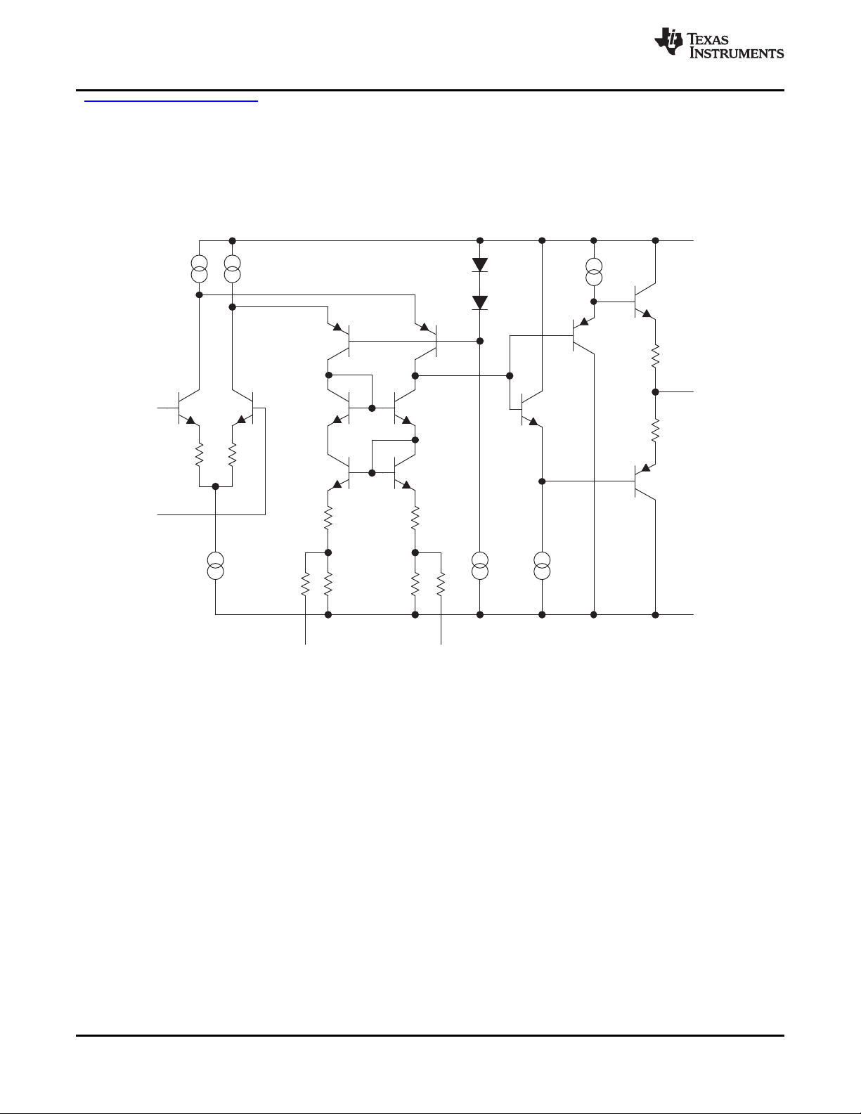
The THS403x is a high-speed operational amplifier configured in a voltage feedback architecture. It is built using
a 30-V, dielectrically isolated, complementary bipolar process with NPN and PNP transistors possessing fTs of
several GHz. This results in an exceptionally high-performance amplifier that has wide bandwidth, high slew rate,
fast settling time, and low distortion. A simplified schematic is shown in Figure 51.
Figure 51. THS4031 Simplified Schematic
22 Submit Documentation Feedback Copyright © 1999–2010, Texas Instruments Incorporated
Product Folder Link(s): THS4031 THS4032
_
+
R
F
R
S
R
G
e
Rg
e
Rf
e
Rs
e
n
IN+
Noiseless
IN−
e
ni
e
no
e
ni
+
ǒ
e
n
Ǔ
2
)
ǒ
IN ) R
S
Ǔ
2
)
ǒ
IN– ǒRFø R
G
ǓǓ
2
) 4 kTRs) 4 kTǒRFø R
G
Ǔ
Ǹ
Where:
k = Boltzmann’s constant = 1.380658 × 10
−23
T = Temperature in degrees Kelvin (273 +°C)
RF || RG = Parallel resistance of RF and R
G
eno+ eniAV+ e
ni
ǒ
1 )
R
F
R
G
Ǔ
(Noninverting Case)
THS4031
THS4032
www.ti.com
查询"THS4031M"供应商
SLOS224G –JULY 1999–REVISED MARCH 2010
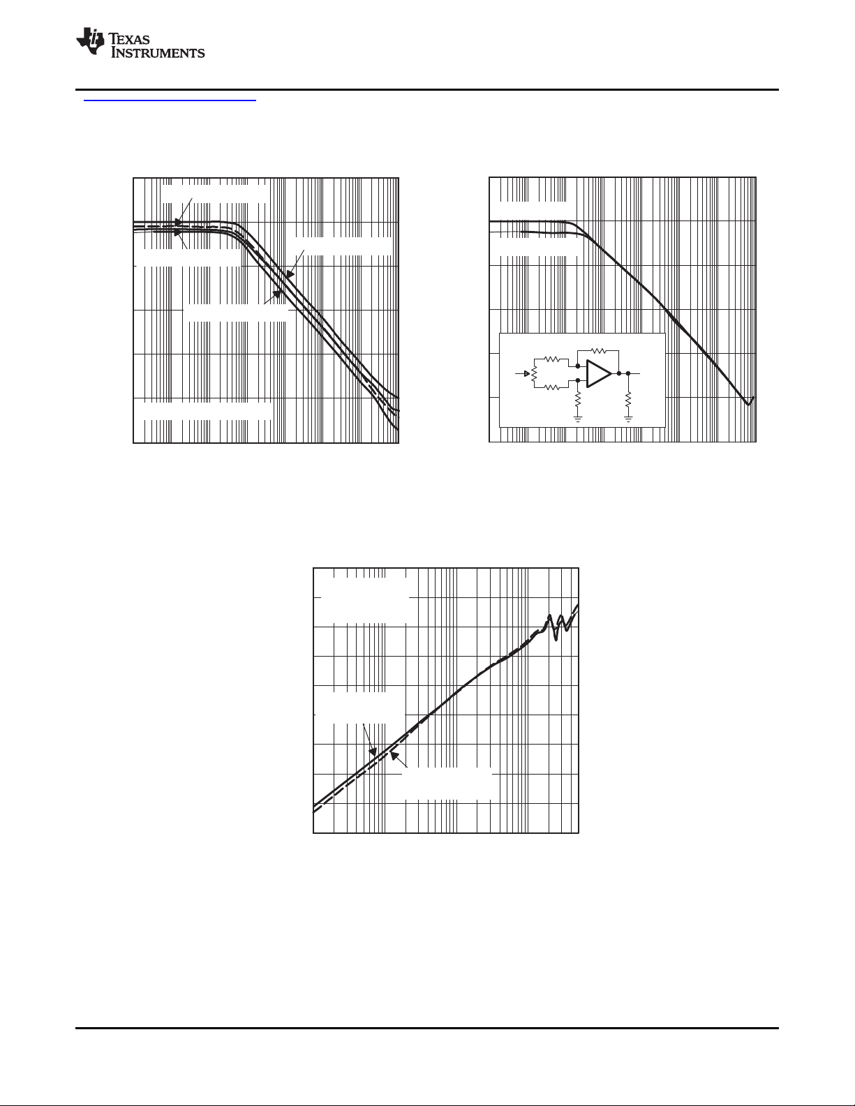
NOISE CALCULATIONS AND NOISE FIGURE
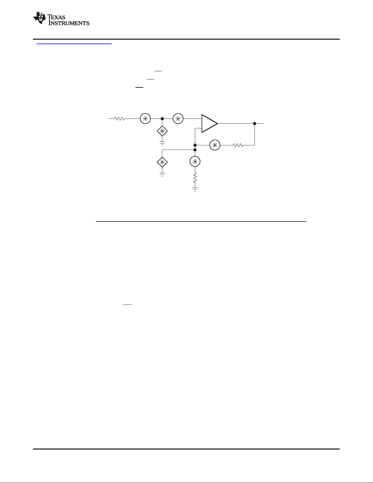
Noise can cause errors on very small signals. This is especially true when amplifying small signals. The noise
model for the THS403x, shown in Figure 52, includes all of the noise sources as follows:
• en= Amplifier internal voltage noise (nV/√Hz)
• IN+ = Noninverting current noise (pA/√Hz)
• IN– = Inverting current noise (pA/√Hz)
• eRx= Thermal voltage noise associated with each resistor (eRx= 4 kTRx)
Figure 52. Noise Model
The total equivalent input noise density (eni) is calculated by using the following equation:
(1)
To get the equivalent output noise of the amplifier, just multiply the equivalent input noise density (eni) by the
overall amplifier gain (AV).
(2)
As the previous equations show, to keep noise at a minimum, small-value resistors should be used. As the
closed-loop gain is increased (by reducing RG), the input noise is reduced considerably because of the parallel
resistance term. This leads to the general conclusion that the most dominant noise sources are the source
resistor (RS) and the internal amplifier noise voltage (en). Because noise is summed in a root-mean-squares
method, noise sources smaller than 25% of the largest noise source can be effectively ignored. This advantage
can greatly simplify the formula and make noise calculations much easier to calculate.
For more information on noise analysis, refer to the application note, Noise Analysis for High-Speed Op Amps
(SBOA066).
Copyright © 1999–2010, Texas Instruments Incorporated Submit Documentation Feedback 23
Product Folder Link(s): THS4031 THS4032

_
+
150 Ω
V
O
V
I
50 Ω
C
i−
300 Ω
7
6
2
0
100 k 1 M 10 M
Output Amplitude − dB
8
9
f − Frequency − Hz
OUTPUT AMPLITUDE
vs
FREQUENCY
10
100 M 500 M
5
4
3
1
C
i−
= 10 pF
No C
i−
(Stray C Only)
VCC = ± 15 V
Gain = 2
RF = 300 Ω
RL = 150 Ω
V
O(PP)
= 0.4 V
300 Ω
_
+
360 Ω
150 Ω
V
O
V
I
56 Ω
C
i−
360 Ω
1
0
−4
−6
100 k 1 M 10 M
Output Amplitude − dB
2
3
f − Frequency − Hz
OUTPUT AMPLITUDE
vs
FREQUENCY
4
100 M 500 M
−1
−2
−3
−5
Ci−= 10 pF
No C
i−
(Stray C Only)
VCC = ± 15 V
Gain = −1
RF = 360 Ω
RL = 150 Ω
V
O(PP)
= 0.4 V
THS4031
THS4032
SLOS224G –JULY 1999–REVISED MARCH 2010
查询"THS4031M"供应商
www.ti.com
OPTIMIZING FREQUENCY RESPONSE
Internal frequency compensation of the THS403x was selected to provide very wide bandwidth performance and
still maintain a very low noise floor. In order to meet these performance requirements, the THS403x must have a
minimum gain of 2 (–1). Because everything is referred to the noninverting terminal of an operational amplifier,
the noise gain in a G = –1 configuration is the same as a G = 2 configuration.
One of the keys to maintaining a smooth frequency response, and hence, a stable pulse response, is to pay
particular attention to the inverting terminal. Any stray capacitance at this node causes peaking in the frequency
response (see Figure 53 and Figure 54). Two things can be done to help minimize this effect. The first is to
simply remove any ground planes under the inverting terminal of the amplifier, including the trace that connects
to this terminal. Additionally, the length of this trace should be minimized. The capacitance at this node causes a
lag in the voltage being fed back due to the charging and discharging of the stray capacitance. If this lag
becomes too long, the amplifier will not be able to correctly keep the noninverting terminal voltage at the same
potential as the inverting terminal's voltage. Peaking and possible oscillations will then occur if this happens.
The second precaution to help maintain a smooth frequency response is to keep the feedback resistor (Rf) and
the gain resistor (Rg) values fairly low. These two resistors are effectively in parallel when looking at the ac
small-signal response. But, as can be seen in Figure 26 through Figure 37, a value too low starts to reduce the
bandwidth of the amplifier. Table 1 shows some recommended feedback resistors to be used with the THS403x.
24 Submit Documentation Feedback Copyright © 1999–2010, Texas Instruments Incorporated
Figure 53. Figure 54.
Table 1. Recommended Feedback Resistors
GAIN Rffor VCC= ±15 V and ±5 V
1 50 Ω
2 300 Ω
–1 360 Ω
5 3.3 kΩ (low stray-c PCB only)
Product Folder Link(s): THS4031 THS4032
+
_
THS403x
C
LOAD
360 Ω
Input
Output
360 Ω
20 Ω
THS4031
THS4032
www.ti.com
查询"THS4031M"供应商
SLOS224G –JULY 1999–REVISED MARCH 2010
DRIVING A CAPACITIVE LOAD
Driving capacitive loads with high-performance amplifiers is not a problem as long as certain precautions are
taken. The first is to realize that the THS403x has been internally compensated to maximize its bandwidth and
slew-rate performance. When the amplifier is compensated in this manner, capacitive loading directly on the
output will decrease the phase margin of the device leading to high-frequency ringing or oscillations. Therefore,
for capacitive loads of greater than 10 pF, it is recommended that a resistor be placed in series with the output of
the amplifier, as shown in Figure 55. A minimum value of 20 Ω should work well for most applications. For
example, in 75-Ω transmission systems, setting the series resistor value to 75 Ω both isolates any capacitance
loading and provides the proper line impedance matching at the source end.
Figure 55. Driving a Capacitive Load
Copyright © 1999–2010, Texas Instruments Incorporated Submit Documentation Feedback 25
Product Folder Link(s): THS4031 THS4032

_
+
THS4031
VCC−
VCC+
10k
Ω
0.1 Fm
0.1 Fm
7
8
4
1
2
3
THS4031
THS4032
SLOS224G –JULY 1999–REVISED MARCH 2010
查询"THS4031M"供应商
www.ti.com
OFFSET NULLING
The THS403x has very low input offset voltage for a high speed amplifier. However, if additional correction is
required, the designer can make use of an offset nulling function provided on the THS4031. By placing a
potentiometer between terminals 1 and 8 of the device and tying the wiper to the negative supply, the input offset
can be adjusted. This is shown in Figure 56.
Figure 56. Offset Nulling Schematic
OFFSET VOLTAGE
The output offset voltage (VOO) is the sum of the input offset voltage (VIO) and both input bias currents (IIB) times
the corresponding gains. The following schematic and formula can be used to calculate the output offset voltage:
Figure 57. Output Offset Voltage Model
26 Submit Documentation Feedback Copyright © 1999–2010, Texas Instruments Incorporated
Product Folder Link(s): THS4031 THS4032

V
I
V
O
C1
+
−
R
G
R
F
R1
f
–3dB
+
1
2pR1C1
V
O
V
I
+ ǒ1)
R
F
R
G
Ǔ
ǒ
1
1) sR1C1
Ǔ
V
I
C2
R2R1
C1
R
F
R
G
R1 = R2 = R
C1 = C2 = C
Q = Peaking Factor
(Butterworth Q = 0.707)
(
=
1
Q
2 –
)
R
G
R
F
_
+
f
–3dB
+
1
2pRC
THS4031
THS4032
www.ti.com
查询"THS4031M"供应商
SLOS224G –JULY 1999–REVISED MARCH 2010
GENERAL CONFIGURATIONS
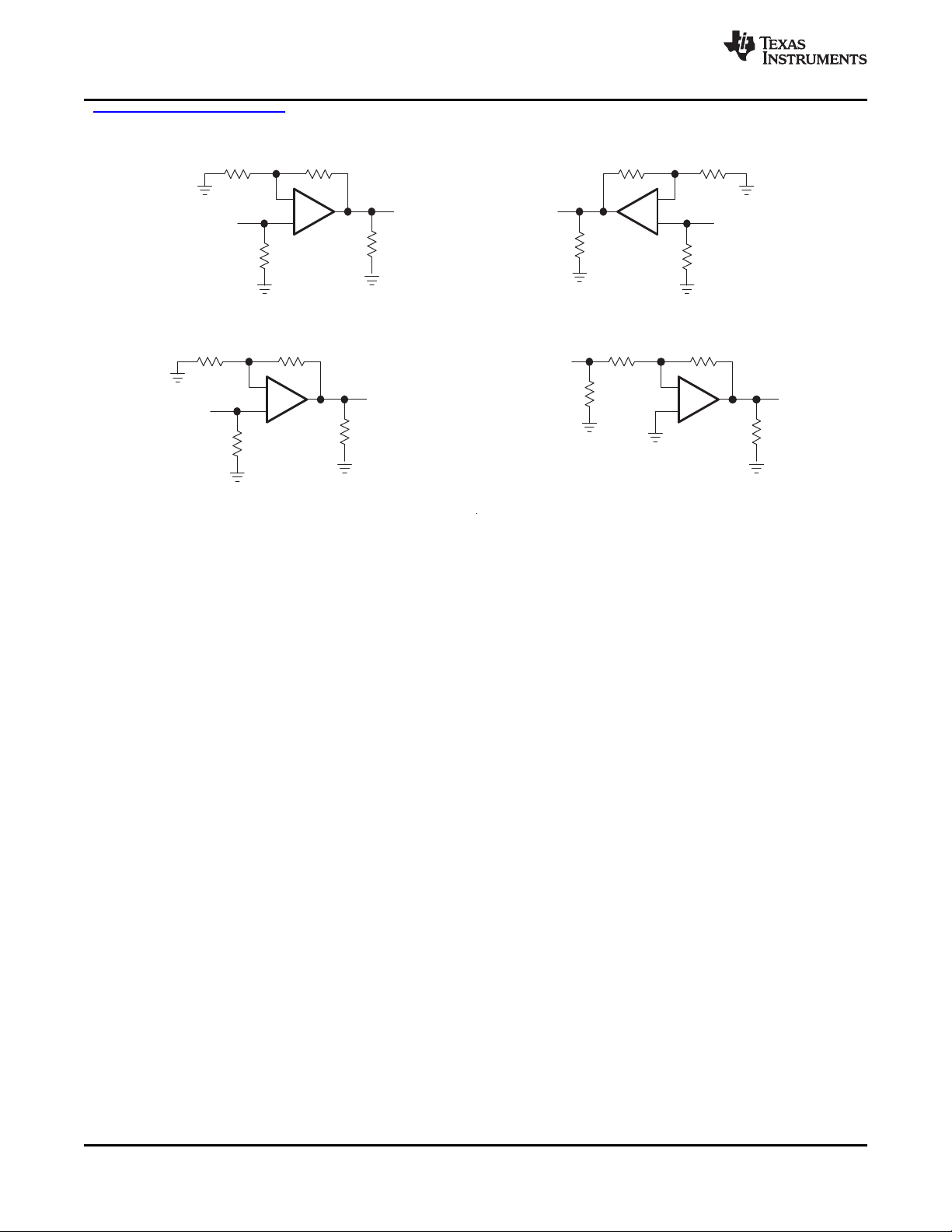
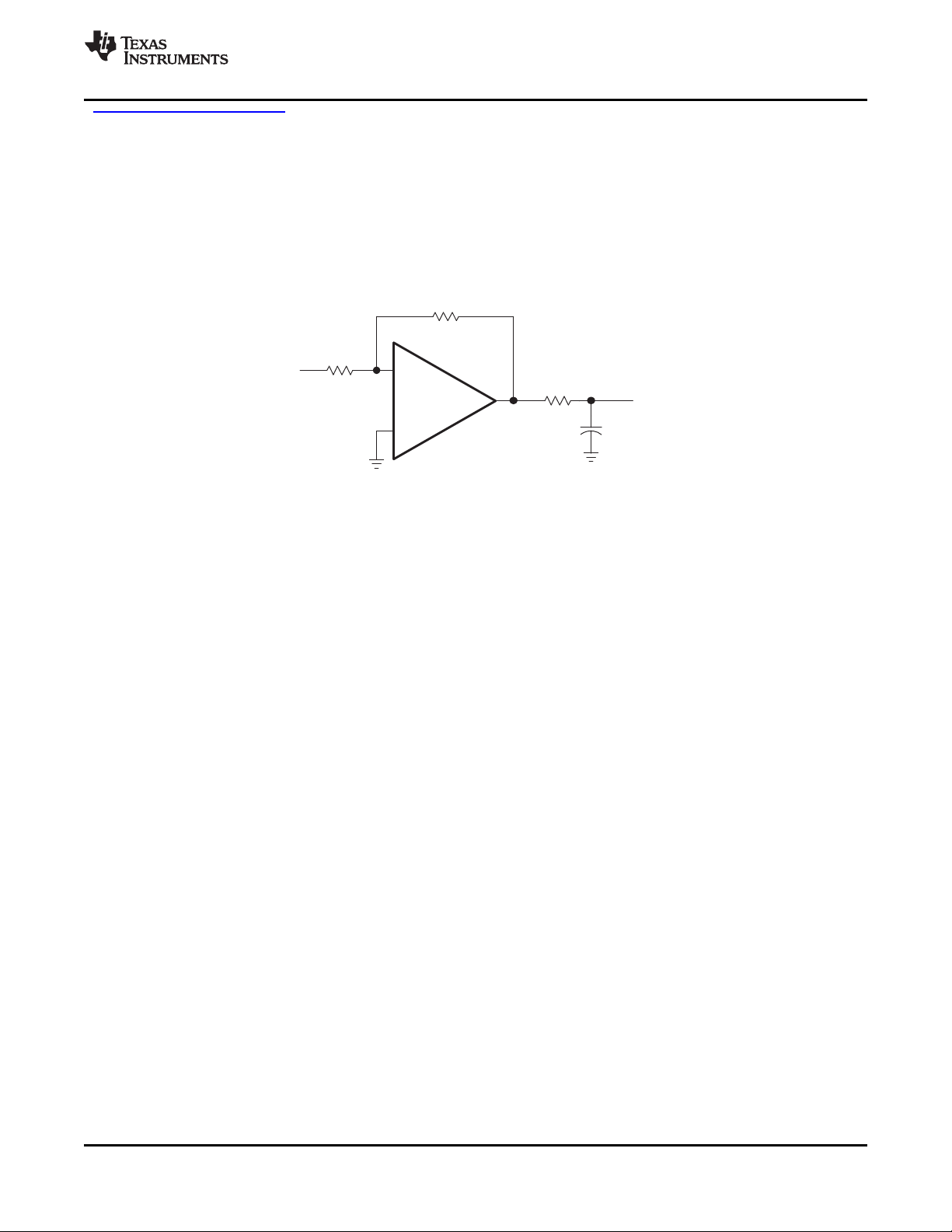
When receiving low-level signals, limiting the bandwidth of the incoming signals into the system is often required.
The simplest way to accomplish this is to place an RC filter at the noninverting terminal of the amplifer (see
Figure 58).
Figure 58. Single-Pole Low-Pass Filter
If even more attenuation is needed, a multiple-pole filter is required. The Sallen-Key filter can be used for this
task. For best results, the amplifier should have a bandwidth that is 8 to 10 times the filter frequency bandwidth.
Otherwise, phase shift of the amplifier can occur.
Figure 59. Two-Pole Low-Pass Sallen-Key Filter
Copyright © 1999–2010, Texas Instruments Incorporated Submit Documentation Feedback 27
Product Folder Link(s): THS4031 THS4032

DIE
Side View (a)
End View (b) Bottom View (c)
DIE
Thermal
Pad
THS4031
THS4032
SLOS224G –JULY 1999–REVISED MARCH 2010
查询"THS4031M"供应商
www.ti.com
CIRCUIT-LAYOUT CONSIDERATIONS
In order to achieve the levels of high-frequency performance of the THS403x, it is essential that proper
printed-circuit board (PCB) high-frequency design techniques be followed. A general set of guidelines is given
below. In addition, a THS403x evaluation board is available to use as a guide for layout or for evaluating the
device performance.
• Ground planes: It is highly recommended that a ground plane be used on the board to provide all
components with a low inductive ground connection. However, in the areas of the amplifier inputs and output,
the ground plane can be removed to minimize the stray capacitance.
• Proper power-supply decoupling: Use a 6.8-mF tantalum capacitor in parallel with a 0.1-mF ceramic capacitor
on each supply terminal. It may be possible to share the tantalum among several amplifiers depending on the
application, but a 0.1-mF ceramic capacitor should always be used on the supply terminal of every amplifier.
In addition, the 0.1-mF capacitor should be placed as close as possible to the supply terminal. As this distance
increases, the inductance in the connecting trace makes the capacitor less effective. The designer should
strive for distances of less than 0.1 inch between the device power terminals and the ceramic capacitors.
• Sockets: Sockets are not recommended for high-speed operational amplifiers. The additional lead inductance
in the socket pins will often lead to stability problems. Surface-mount packages soldered directly to the
printed-circuit board is the best implementation.
• Short trace runs/compact part placements: Optimum high-frequency performance is achieved when stray
series inductance has been minimized. To realize this, the circuit layout should be made as compact as
possible, thereby minimizing the length of all trace runs. Particular attention should be paid to the inverting
input of the amplifier. Its length should be kept as short as possible. This will help to minimize stray
capacitance at the input of the amplifier.
• Surface-mount passive components: Using surface-mount passive components is recommended for
high-frequency amplifier circuits for several reasons. First, because of the extremely low lead inductance of
surface-mount components, the problem with stray series inductance is greatly reduced. Second, the small
size of surface-mount components naturally leads to a more compact layout thereby minimizing both stray
inductance and capacitance. If leaded components are used, it is recommended that the lead lengths be kept
as short as possible.
GENERAL PowerPAD™ DESIGN CONSIDERATIONS
The THS403x is available in a thermally-enhanced DGN package, which is a member of the PowerPAD family of
packages. This package is constructed using a downset leadframe upon which the die is mounted [see
Figure 60(a) and Figure 60(b)]. This arrangement results in the leadframe being exposed as a thermal pad on
the underside of the package [see Figure 60(c)]. Because this thermal pad has direct thermal contact with the
die, excellent thermal performance can be achieved by providing a good thermal path away from the thermal
pad.
The PowerPAD package allows for both assembly and thermal management in one manufacturing operation.
During the surface-mount solder operation (when the leads are being soldered), the thermal pad can also be
soldered to a copper area underneath the package. Through the use of thermal paths within this copper area,
heat can be conducted away from the package into either a ground plane or other heat-dissipating device.
The PowerPAD package represents a breakthrough in combining the small area and ease of assembly of
surface mount with the heretofore awkward mechanical methods of heatsinking.
A. The thermal pad is electrically isolated from all terminals in the package.
Figure 60. Views of Thermally-Enhanced DGN Package
28 Submit Documentation Feedback Copyright © 1999–2010, Texas Instruments Incorporated
Product Folder Link(s): THS4031 THS4032

Thermal pad area (68 mils x 70 mils) with 5 vias
(Via diameter = 13 mils)
THS4031
THS4032
www.ti.com
查询"THS4031M"供应商
SLOS224G –JULY 1999–REVISED MARCH 2010
Although there are many ways to properly heatsink this device, the following steps illustrate the recommended
approach.
Figure 61. PowerPAD™ PCB Etch and Via Pattern
1. Prepare the PCB with a top-side etch pattern as shown in Figure 61. There should be etch for the leads as
well as etch for the thermal pad.
2. Place five holes in the area of the thermal pad. These holes should be 13 mils (0,3302 mm) in diameter.
They are kept small so that solder wicking through the holes is not a problem during reflow.
3. Additional vias may be placed anywhere along the thermal plane outside of the thermal pad area. This helps
dissipate the heat generated by the THS403xDGN IC. These additional vias may be larger than the 13-mil
diameter vias directly under the thermal pad. They can be larger because they are not in the thermal pad
area to be soldered so that wicking is not a problem.
4. Connect all holes to the internal ground plane.
5. When connecting these holes to the ground plane, do not use the typical web or spoke via connection
methodology. Web connections have a high thermal-resistance connection that is useful for slowing the heat
transfer during soldering operations. This makes the soldering of vias that have plane connections easier. In
this application, however, low thermal resistance is desired for the most efficient heat transfer. Therefore, the
holes under the THS403xDGN package should connect to the internal ground plane with a complete
connection around the entire circumference of the plated-through hole.
6. The top-side solder mask should leave the terminals of the package and the thermal pad area with its five
holes exposed. The bottom-side solder mask should cover the five holes of the thermal pad area, which
prevents solder from being pulled away from the thermal pad area during the reflow process.
7. Apply solder paste to the exposed thermal pad area and to all the IC terminals.
8. With these preparatory steps in place, the THS403xDGN IC is simply placed in position and run through the
solder reflow operation as any standard surface-mount component. This results in a part that is properly
installed.
Copyright © 1999–2010, Texas Instruments Incorporated Submit Documentation Feedback 29
Product Folder Link(s): THS4031 THS4032

P
D
+
ǒ
T
MAX–TA
q
JA
Ǔ
Where:
P
D
= Maximum power dissipation of THS403x IC (watts)
T
MAX
= Absolute maximum operating junction temperature (125°C)
T
A
= Free-ambient air temperature (°C)
θ
JA
= θ
JC
+ θ
CA
θ
JC
= Thermal coefficient from junction to case
θ
CA
= Thermal coefficient from case to ambient air (°C/W)
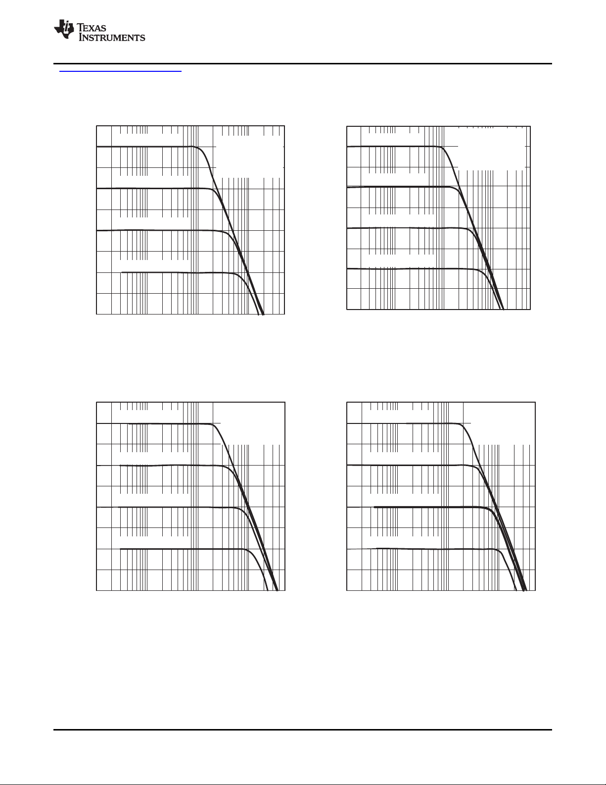
MAXIMUMPOWERDISSIPATION
AMBIENTTEMPERATURE
vs
0
0.5
1
1.5
2
2.5
3
-40 -20 0 20 40 60 80 100
TA-Free AirTemperature-°C
MaximumPowerDissipation-W
DGNPackage
=58.4ºC/W2oz.
TraceandCopperPad
WithSolder
q
JA
T =130ºC
J
DGNPackage
=158.4ºC/W2oz.
TraceandCopperPad
WithoutSolder
q
JA
SOICPackage
High-KTestPCB
=98ºC/Wq
JA
SOICPackage
High-KTestPCB
=166.7ºC/Wq
JA
THS4031
THS4032
SLOS224G –JULY 1999–REVISED MARCH 2010
查询"THS4031M"供应商
www.ti.com
The actual thermal performance achieved with the THS403xDGN in its PowerPAD™ package depends on the
application. In the example above, if the size of the internal ground plane is approximately 3 inches × 3 inches
(7,62 cm × 7,62 cm), then the expected thermal coefficient, qJA, is about 58.4°C/W. For comparison, the
non-PowerPAD™ version of the THS403x IC (SOIC) is shown. For a given qJA, the maximum power dissipation
is shown in Figure 62 and is calculated by the following formula:
(3)
Results are with no air flow and PCB size = 3”× 3” (7,62 cm x 7,62 cm)
Figure 62. Maximum Power Dissipation vs Free-Air Temperature
More complete details of the PowerPAD installation process and thermal management techniques can be found
in the Texas Instruments technical brief, PowerPAD™ Thermally-Enhanced Package (SLMA002). This document
can be found at the TI web site (www.ti.com) by searching on the key word PowerPAD. The document can also
be ordered through your local TI sales office. Refer to literature number SLMA002 when ordering.
The next thing to be considered is package constraints. The two sources of heat within an amplifier are quiescent
power and output power. The designer should never forget about the quiescent heat generated within the device,
especially multiamplifier devices. Because these devices have linear output stages (Class A-B), most of the heat
dissipation is at low output voltages with high output currents. Figure 63 to Figure 66 shows this effect, along with
the quiescent heat, with an ambient air temperature of 50°C. When using VCC= ±5 V, heat is generally not a
problem, even with SOIC packages. But, when using VCC= ±15 V, the SOIC package is severely limited in the
amount of heat it can dissipate. The other key factor when looking at these graphs is how the devices are
mounted on the PCB. The PowerPAD™ devices are extremely useful for heat dissipation. But, the device should
30 Submit Documentation Feedback Copyright © 1999–2010, Texas Instruments Incorporated
Product Folder Link(s): THS4031 THS4032

10
100
1000
0 3 6
9
12 15
|V |-RMSOutputVoltage-V
out
|I |-MaximumRMSOutputCurrent-mA
out
MAXIMUMRMSOUTPUTCURRENT
vs
RMSOUTPUTVOLTAGEDUETOTHERMAL LIMITS
T =130°C
T =50°C
J
A
DGNPackage
=58.4°C/Wq
JA
MaximumOutput
CurrentLimitLine
V =±15V
CC
SO-8Package
=167°C/W
Low-KTestPCB
q
JA
SO-8Package
=98°C/W
High-KTestPCB
q
JA
MAXIMUMRMSOUTPUTCURRENT
RMSOUTPUTVOLTAGEDUETOTHERMAL LIMITS
vs
0
20
40
60
80
100
120
140
160
180
200
0 1 2 3 4 5
V =±5V
T =130°C
T =50°C
CC
J
A
SO-8
=121°C/W
High-KTestPCB
q
JA
PackageWith
<=120°C/Wq
JA
SO-8
=167°C/W
Low-KTestPCB
q
JA
|V |-RMSOutputVoltage-V
out
|I |MaximumRMSOutputCurrent-mA
out
MaximumOutput
CurrentLimitLine
1
10
100
1000
0 3 6 9 12 15
|I |-MaximumRMSOutputCurrent-mA
out
|V |-RMSOutputVoltage-V
out
BothChannels
T =130°C
T =50°C
J
A
MaximumOutput
CurrentLimitsLine
THS4032
V =±15V
CC
DGNPackage
=58.4°C/Wq
JA
SO-8Package
=167°C/W
Low-KTestPCB
q
JA
SO-8Package
=98°C/W
High-KTestPCB
q
JA
Safe
Operating
Area
MAXIMUMRMSOUTPUTCURRENT
vs
RMSOUTPUTVOLTAGEDUETOTHERMAL LIMITS
0
20
40
60
80
100
120
140
160
180
200
0 1 2 3 4 5
|V |-RMSOutputVoltage-V
out
|I |-MaximumRMSOutputCurrent-mA
out
PackageWith
<=60°C/Wq
JA
MaximumOutput
CurrentLimitLine
DGNPackage
=58.4°C/Wq
JA
THS4032
V =±5V
CC
Safe
Operating
Area
SO-8Package
=167°C/W
Low-KTestPCB
q
JA
SO-8Package
=98°C/W
High-KTestPCB
q
JA
BothChannels
T =130°C
T =50°C
J
A
MAXIMUMRMSOUTPUTCURRENT
vs
RMSOUTPUTVOLTAGEDUETOTHERMAL LIMITS
THS4031
THS4032
www.ti.com
查询"THS4031M"供应商
SLOS224G –JULY 1999–REVISED MARCH 2010
always be soldered to a copper plane to fully use the heat dissipation properties of the PowerPAD™. The SOIC
package, on the other hand, is highly dependent on how it is mounted on the PCB. As more trace and copper
area is placed around the device, qJAdecreases and the heat dissipation capability increases. The currents and
voltages shown in these graphs are for the total package. For the dual amplifier package (THS4032), the sum of
the RMS output currents and voltages should be used to choose the proper package.
Figure 63. Figure 64.
Copyright © 1999–2010, Texas Instruments Incorporated Submit Documentation Feedback 31
Figure 65. Figure 66.
Product Folder Link(s): THS4031 THS4032

_
+
THS4031
VCC−
VCC+
C1
6.8 µF
C4
0.1 µF
C2
6.8 µF
C3
0.1 µF
R4
301 Ω
R2
301 Ω
R3
49.9 Ω
R5
49.9 Ω
R4
49.9 Ω
IN−
IN+
NULL
OUT
NULL
+
+
THS4031
THS4032
SLOS224G –JULY 1999–REVISED MARCH 2010
查询"THS4031M"供应商
www.ti.com
EVALUATION BOARD
An evaluation board is available for the THS4031 (literature number SLOP203) and THS4032 (literature number
SLOP135). This board has been configured for very low parasitic capacitance in order to realize the full
performance of the amplifier. A schematic of the evaluation board is shown in Figure 67. The circuitry has been
designed so that the amplifier may be used in either an inverting or noninverting configuration. For more
information, refer to the THS4031 EVM User's Guide (SLOU038) or the THS4032 EVM User's Guide (SLOU039).
To order the evaluation board, contact your local TI sales office or distributor.
Figure 67. THS4031 Evaluation Board
32 Submit Documentation Feedback Copyright © 1999–2010, Texas Instruments Incorporated
Product Folder Link(s): THS4031 THS4032
THS4031
THS4032
www.ti.com
查询"THS4031M"供应商
SLOS224G –JULY 1999–REVISED MARCH 2010
REVISION HISTORY
NOTE: Page numbers for previous revisions may differ from page numbers in the current version.
Changes from Revision F (September, 2008) to Revision G Page
• Changed units for input voltage noise parameter (+25°C specifications) from nA/√Hz to nV√Hz ....................................... 4
• Changed units for input voltage noise parameter (full range of TAspecifications) from nA/√Hz to nV√Hz .......................... 6
Changes from Revision E (June, 2007) to Revision F Page
• Deleted bullet point for Stable in Gain of 2 (–1) or greater ................................................................................................... 1
• Editorial changes to paragraph format ................................................................................................................................ 28
Copyright © 1999–2010, Texas Instruments Incorporated Submit Documentation Feedback 33
Product Folder Link(s): THS4031 THS4032
PACKAGE OPTION ADDENDUM
查询"THS4031M"供应商
www.ti.com 3-Mar-2010
PACKAGING INFORMATION
Orderable Device Status
5962-9959501Q2A ACTIVE LCCC FK 20 1 TBD POST-PLATE N / A for Pkg Type
5962-9959501QPA ACTIVE CDIP JG 8 1 TBD A42 N / A for Pkg Type
THS4031CD ACTIVE SOIC D 8 75 Green (RoHS &
THS4031CDG4 ACTIVE SOIC D 8 75 Green (RoHS &
THS4031CDGN ACTIVE MSOP-
THS4031CDGNG4 ACTIVE MSOP-
THS4031CDGNR ACTIVE MSOP-
THS4031CDGNRG4 ACTIVE MSOP-
THS4031CDR ACTIVE SOIC D 8 2500 Green (RoHS &
THS4031CDRG4 ACTIVE SOIC D 8 2500 Green (RoHS &
THS4031ID ACTIVE SOIC D 8 75 Green (RoHS &
THS4031IDG4 ACTIVE SOIC D 8 75 Green (RoHS &
THS4031IDGN ACTIVE MSOP-
THS4031IDGNG4 ACTIVE MSOP-
THS4031IDGNR ACTIVE MSOP-
THS4031IDGNRG4 ACTIVE MSOP-
THS4031IDR ACTIVE SOIC D 8 2500 Green (RoHS &
THS4031IDRG4 ACTIVE SOIC D 8 2500 Green (RoHS &
THS4031MFKB ACTIVE LCCC FK 20 1 TBD POST-PLATE N / A for Pkg Type
THS4031MJG ACTIVE CDIP JG 8 1 TBD A42 N / A for Pkg Type
THS4031MJGB ACTIVE CDIP JG 8 1 TBD A42 N / A for Pkg Type
THS4032CD ACTIVE SOIC D 8 75 Green (RoHS &
THS4032CDG4 ACTIVE SOIC D 8 75 Green (RoHS &
THS4032CDGN ACTIVE MSOP- DGN 8 80 Green (RoHS & CU NIPDAU Level-1-260C-UNLIM
(1)
Package
Type
Power
PAD
Power
PAD
Power
PAD
Power
PAD
Power
PAD
Power
PAD
Power
PAD
Power
PAD
Package
Drawing
DGN 8 80 Green (RoHS &
DGN 8 80 Green (RoHS &
DGN 8 2500 Green (RoHS &
DGN 8 2500 Green (RoHS &
DGN 8 80 Green (RoHS &
DGN 8 80 Green (RoHS &
DGN 8 2500 Green (RoHS &
DGN 8 2500 Green (RoHS &
Pins Package
Qty
Eco Plan
no Sb/Br)
no Sb/Br)
no Sb/Br)
no Sb/Br)
no Sb/Br)
no Sb/Br)
no Sb/Br)
no Sb/Br)
no Sb/Br)
no Sb/Br)
no Sb/Br)
no Sb/Br)
no Sb/Br)
no Sb/Br)
no Sb/Br)
no Sb/Br)
no Sb/Br)
no Sb/Br)
(2)
Lead/Ball Finish MSL Peak Temp
CU NIPDAU Level-1-260C-UNLIM
CU NIPDAU Level-1-260C-UNLIM
CU NIPDAU Level-1-260C-UNLIM
CU NIPDAU Level-1-260C-UNLIM
CU NIPDAU Level-1-260C-UNLIM
CU NIPDAU Level-1-260C-UNLIM
CU NIPDAU Level-1-260C-UNLIM
CU NIPDAU Level-1-260C-UNLIM
CU NIPDAU Level-1-260C-UNLIM
CU NIPDAU Level-1-260C-UNLIM
CU NIPDAU Level-1-260C-UNLIM
CU NIPDAU Level-1-260C-UNLIM
CU NIPDAU Level-1-260C-UNLIM
CU NIPDAU Level-1-260C-UNLIM
CU NIPDAU Level-1-260C-UNLIM
CU NIPDAU Level-1-260C-UNLIM
CU NIPDAU Level-1-260C-UNLIM
CU NIPDAU Level-1-260C-UNLIM
(3)
Addendum-Page 1

PACKAGE OPTION ADDENDUM
查询"THS4031M"供应商
www.ti.com 3-Mar-2010
Orderable Device Status
(1)
Package
Type
Power
Package
Drawing
Pins Package
Qty
Eco Plan
no Sb/Br)
(2)
Lead/Ball Finish MSL Peak Temp
(3)
PAD
THS4032CDGNG4 ACTIVE MSOP-
Power
DGN 8 80 Green (RoHS &
no Sb/Br)
CU NIPDAU Level-1-260C-UNLIM
PAD
THS4032CDR ACTIVE SOIC D 8 2500 Green (RoHS &
CU NIPDAU Level-1-260C-UNLIM
no Sb/Br)
THS4032CDRG4 ACTIVE SOIC D 8 2500 Green (RoHS &
CU NIPDAU Level-1-260C-UNLIM
no Sb/Br)
THS4032ID ACTIVE SOIC D 8 75 Green (RoHS &
CU NIPDAU Level-1-260C-UNLIM
no Sb/Br)
THS4032IDG4 ACTIVE SOIC D 8 75 Green (RoHS &
CU NIPDAU Level-1-260C-UNLIM
no Sb/Br)
THS4032IDGN ACTIVE MSOP-
Power
DGN 8 80 Green (RoHS &
no Sb/Br)
CU NIPDAU Level-1-260C-UNLIM
PAD
THS4032IDGNG4 ACTIVE MSOP-
Power
DGN 8 80 Green (RoHS &
no Sb/Br)
CU NIPDAU Level-1-260C-UNLIM
PAD
THS4032IDGNR ACTIVE MSOP-
Power
DGN 8 2500 Green (RoHS &
no Sb/Br)
CU NIPDAU Level-1-260C-UNLIM
PAD
THS4032IDGNRG4 ACTIVE MSOP-
Power
DGN 8 2500 Green (RoHS &
no Sb/Br)
CU NIPDAU Level-1-260C-UNLIM
PAD
THS4032IDR ACTIVE SOIC D 8 2500 Green (RoHS &
CU NIPDAU Level-1-260C-UNLIM
no Sb/Br)
THS4032IDRG4 ACTIVE SOIC D 8 2500 Green (RoHS &
CU NIPDAU Level-1-260C-UNLIM
no Sb/Br)
(1)
The marketing status values are defined as follows:
ACTIVE: Product device recommended for new designs.
LIFEBUY: TI has announced that the device will be discontinued, and a lifetime-buy period is in effect.
NRND: Not recommended for new designs. Device is in production to support existing customers, but TI does not recommend using this part in
a new design.
PREVIEW: Device has been announced but is not in production. Samples may or may not be available.
OBSOLETE: TI has discontinued the production of the device.
(2)
Eco Plan - The planned eco-friendly classification: Pb-Free (RoHS), Pb-Free (RoHS Exempt), or Green (RoHS & no Sb/Br) - please check
http://www.ti.com/productcontent for the latest availability information and additional product content details.
TBD: The Pb-Free/Green conversion plan has not been defined.
Pb-Free (RoHS): TI's terms "Lead-Free" or "Pb-Free" mean semiconductor products that are compatible with the current RoHS requirements
for all 6 substances, including the requirement that lead not exceed 0.1% by weight in homogeneous materials. Where designed to be soldered
at high temperatures, TI Pb-Free products are suitable for use in specified lead-free processes.
Pb-Free (RoHS Exempt): This component has a RoHS exemption for either 1) lead-based flip-chip solder bumps used between the die and
package, or 2) lead-based die adhesive used between the die and leadframe. The component is otherwise considered Pb-Free (RoHS
compatible) as defined above.
Green (RoHS & no Sb/Br): TI defines "Green" to mean Pb-Free (RoHS compatible), and free of Bromine (Br) and Antimony (Sb) based flame
retardants (Br or Sb do not exceed 0.1% by weight in homogeneous material)
(3)
MSL, Peak Temp. -- The Moisture Sensitivity Level rating according to the JEDEC industry standard classifications, and peak solder
temperature.
Important Information and Disclaimer:The information provided on this page represents TI's knowledge and belief as of the date that it is
provided. TI bases its knowledge and belief on information provided by third parties, and makes no representation or warranty as to the
accuracy of such information. Efforts are underway to better integrate information from third parties. TI has taken and continues to take
Addendum-Page 2
PACKAGE OPTION ADDENDUM
查询"THS4031M"供应商
www.ti.com 3-Mar-2010
reasonable steps to provide representative and accurate information but may not have conducted destructive testing or chemical analysis on
incoming materials and chemicals. TI and TI suppliers consider certain information to be proprietary, and thus CAS numbers and other limited
information may not be available for release.
In no event shall TI's liability arising out of such information exceed the total purchase price of the TI part(s) at issue in this document sold by TI
to Customer on an annual basis.
OTHER QUALIFIED VERSIONS OF THS4031, THS4031M, THS4032 :
Enhanced Product: THS4032-EP
•
NOTE: Qualified Version Definitions:
Enhanced Product - Supports Defense, Aerospace and Medical Applications
•
Addendum-Page 3
PACKAGE MATERIALS INFORMATION
查询"THS4031M"供应商
www.ti.com 27-Sep-2010
TAPE AND REEL INFORMATION
*All dimensions are nominal
Device Package
THS4031CDR SOIC D 8 2500 330.0 12.4 6.4 5.2 2.1 8.0 12.0 Q1
THS4031IDR SOIC D 8 2500 330.0 12.4 6.4 5.2 2.1 8.0 12.0 Q1
THS4032CDR SOIC D 8 2500 330.0 12.4 6.4 5.2 2.1 8.0 12.0 Q1
THS4032IDR SOIC D 8 2500 330.0 12.4 6.4 5.2 2.1 8.0 12.0 Q1
Type
Package
Drawing
Pins SPQ Reel
Diameter
(mm)
Reel
Width
W1 (mm)
A0
(mm)B0(mm)K0(mm)P1(mm)W(mm)
Pin1
Quadrant
Pack Materials-Page 1
PACKAGE MATERIALS INFORMATION
查询"THS4031M"供应商
www.ti.com 27-Sep-2010
*All dimensions are nominal
Device Package Type Package Drawing Pins SPQ Length (mm) Width (mm) Height (mm)
THS4031CDR SOIC D 8 2500 346.0 346.0 29.0
THS4031IDR SOIC D 8 2500 346.0 346.0 29.0
THS4032CDR SOIC D 8 2500 346.0 346.0 29.0
THS4032IDR SOIC D 8 2500 346.0 346.0 29.0
Pack Materials-Page 2

MECHANICAL DATA
查询"THS4031M"供应商
MCER001A – JANUARY 1995 – REVISED JANUARY 1997
JG (R-GDIP-T8) CERAMIC DUAL-IN-LINE
0.400 (10,16)
0.355 (9,00)
8
1
0.063 (1,60)
0.015 (0,38)
5
4
0.065 (1,65)
0.045 (1,14)
0.020 (0,51) MIN
0.280 (7,11)
0.245 (6,22)
0.310 (7,87)
0.290 (7,37)
0.200 (5,08) MAX
Seating Plane
0.023 (0,58)
0.015 (0,38)
0.100 (2,54)
NOTES: A. All linear dimensions are in inches (millimeters).
B. This drawing is subject to change without notice.
C. This package can be hermetically sealed with a ceramic lid using glass frit.
D. Index point is provided on cap for terminal identification.
E. Falls within MIL STD 1835 GDIP1-T8
0.130 (3,30) MIN
0°–15°
0.014 (0,36)
0.008 (0,20)
4040107/C 08/96
POST OFFICE BOX 655303 • DALLAS, TEXAS 75265

MECHANICAL DATA
查询"THS4031M"供应商
FK (S-CQCC-N**) LEADLESS CERAMIC CHIP CARRIER
28 TERMINAL SHOWN
MLCC006B – OCTOBER 1996
A SQ
B SQ
19
20
22
23
24
25
21
12826 27
12
1314151618 17
0.020 (0,51)
0.010 (0,25)
MIN
0.342
(8,69)
0.442
0.640
0.739
0.938
1.141
A
0.358
(9,09)
0.458
(11,63)
0.660
(16,76)
0.761
(19,32)(18,78)
0.962
(24,43)
1.165
(29,59)
NO. OF
TERMINALS
**
11
10
9
8
7
6
5
432
20
28
44
52
68
84
0.020 (0,51)
0.010 (0,25)
(11,23)
(16,26)
(23,83)
(28,99)
MINMAX
0.307
(7,80)
0.406
(10,31)
0.495
(12,58)
0.495
(12,58)
0.850
(21,6)
1.047
(26,6)
0.080 (2,03)
0.064 (1,63)
B
MAX
0.358
(9,09)
0.458
(11,63)
0.560
(14,22)
0.560
(14,22)
0.858
(21,8)
1.063
(27,0)
0.055 (1,40)
0.045 (1,14)
0.028 (0,71)
0.022 (0,54)
0.050 (1,27)
NOTES: A. All linear dimensions are in inches (millimeters).
B. This drawing is subject to change without notice.
C. This package can be hermetically sealed with a metal lid.
D. The terminals are gold plated.
E. Falls within JEDEC MS-004
POST OFFICE BOX 655303 • DALLAS, TEXAS 75265
0.045 (1,14)
0.035 (0,89)
0.045 (1,14)
0.035 (0,89)
4040140/D 10/96

查询"THS4031M"供应商

查询"THS4031M"供应商

查询"THS4031M"供应商

查询"THS4031M"供应商

查询"THS4031M"供应商

查询"THS4031M"供应商
IMPORTANT NOTICE
Texas Instruments Incorporated and its subsidiaries (TI) reserve the right to make corrections, modifications, enhancements, improvements,
and other changes to its products and services at any time and to discontinue any product or service without notice. Customers should
obtain the latest relevant information before placing orders and should verify that such information is current and complete. All products are
sold subject to TI’s terms and conditions of sale supplied at the time of order acknowledgment.
TI warrants performance of its hardware products to the specifications applicable at the time of sale in accordance with TI’s standard
warranty. Testing and other quality control techniques are used to the extent TI deems necessary to support this warranty. Except where
mandated by government requirements, testing of all parameters of each product is not necessarily performed.
TI assumes no liability for applications assistance or customer product design. Customers are responsible for their products and
applications using TI components. To minimize the risks associated with customer products and applications, customers should provide
adequate design and operating safeguards.
TI does not warrant or represent that any license, either express or implied, is granted under any TI patent right, copyright, mask work right,
or other TI intellectual property right relating to any combination, machine, or process in which TI products or services are used. Information
published by TI regarding third-party products or services does not constitute a license from TI to use such products or services or a
warranty or endorsement thereof. Use of such information may require a license from a third party under the patents or other intellectual
property of the third party, or a license from TI under the patents or other intellectual property of TI.
Reproduction of TI information in TI data books or data sheets is permissible only if reproduction is without alteration and is accompanied
by all associated warranties, conditions, limitations, and notices. Reproduction of this information with alteration is an unfair and deceptive
business practice. TI is not responsible or liable for such altered documentation. Information of third parties may be subject to additional
restrictions.
Resale of TI products or services with statements different from or beyond the parameters stated by TI for that product or service voids all
express and any implied warranties for the associated TI product or service and is an unfair and deceptive business practice. TI is not
responsible or liable for any such statements.
TI products are not authorized for use in safety-critical applications (such as life support) where a failure of the TI product would reasonably
be expected to cause severe personal injury or death, unless officers of the parties have executed an agreement specifically governing
such use. Buyers represent that they have all necessary expertise in the safety and regulatory ramifications of their applications, and
acknowledge and agree that they are solely responsible for all legal, regulatory and safety-related requirements concerning their products
and any use of TI products in such safety-critical applications, notwithstanding any applications-related information or support that may be
provided by TI. Further, Buyers must fully indemnify TI and its representatives against any damages arising out of the use of TI products in
such safety-critical applications.
TI products are neither designed nor intended for use in military/aerospace applications or environments unless the TI products are
specifically designated by TI as military-grade or "enhanced plastic." Only products designated by TI as military-grade meet military
specifications. Buyers acknowledge and agree that any such use of TI products which TI has not designated as military-grade is solely at
the Buyer's risk, and that they are solely responsible for compliance with all legal and regulatory requirements in connection with such use.
TI products are neither designed nor intended for use in automotive applications or environments unless the specific TI products are
designated by TI as compliant with ISO/TS 16949 requirements. Buyers acknowledge and agree that, if they use any non-designated
products in automotive applications, TI will not be responsible for any failure to meet such requirements.
Following are URLs where you can obtain information on other Texas Instruments products and application solutions:
Products Applications
Amplifiers amplifier.ti.com Audio www.ti.com/audio
Data Converters dataconverter.ti.com Automotive www.ti.com/automotive
DLP® Products www.dlp.com Communications and www.ti.com/communications
DSP dsp.ti.com Computers and www.ti.com/computers
Clocks and Timers www.ti.com/clocks Consumer Electronics www.ti.com/consumer-apps
Interface interface.ti.com Energy www.ti.com/energy
Logic logic.ti.com Industrial www.ti.com/industrial
Power Mgmt power.ti.com Medical www.ti.com/medical
Microcontrollers microcontroller.ti.com Security www.ti.com/security
RFID www.ti-rfid.com Space, Avionics & www.ti.com/space-avionics-defense
RF/IF and ZigBee® Solutions www.ti.com/lprf Video and Imaging www.ti.com/video
Mailing Address: Texas Instruments, Post Office Box 655303, Dallas, Texas 75265
Copyright © 2010, Texas Instruments Incorporated
Telecom
Peripherals
Defense
Wireless www.ti.com/wireless-apps
 Loading...