

T
查询THS1031供应商
THS1031
2.7 V – 5.5 V, 10-BIT, 30 MSPS
CMOS ANALOG-TO-DIGITAL CONVERTER
SLAS242A – NOVEMBER 1999 – REVISED JANUARY 2000
D
10-Bit Resolution 30 MSPS
Analog-to-Digital Converter:
D
Configurable Input Functions:
– Single-Ended
– Single-Ended With Analog Clamp
– Single-Ended With Programmable Digital
Clamp
– Differential
D
Built-in Programmable Gain Amplifier
(PGA)
D
Differential Nonlinearity: ±0.3 LSB
D
Signal-to-Noise: 56 dB
D
Spurious Free Dynamic Range: 60 dB
D
Adjustable Internal Voltage Reference
D
Straight Binary/2s Complement Output
D
Out-of-Range Indicator
D
Power-Down Mode
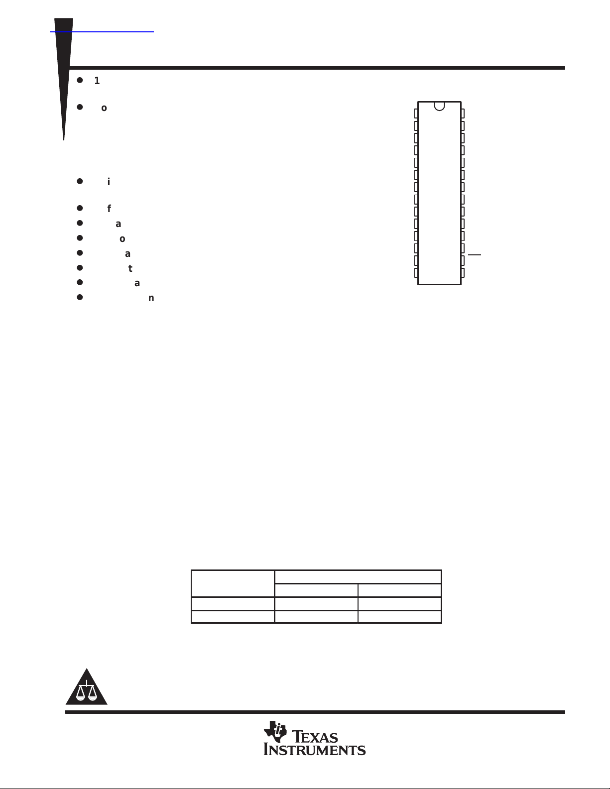
28-PIN TSSOP/SOIC PACKAGE
AGND
DV
DGND
DD
I/O0
I/O1
I/O2
I/O3
I/O4
I/O5
I/O6
I/O7
I/O8
I/O9
OVR
(TOP VIEW)
1
28
2
27
3
26
4
25
5
24
6
23
7
22
8
21
9
20
10
19
11
18
12
17
13
16
14
15
AV
DD
AIN
V
REF
REFBS
REFBF
MODE
REFTF
REFTS
CLAMPIN
CLAMP
REFSENSE
WR
OE
CLK
description
The THS1031 is a CMOS, low power, 10-bit, 30 MSPS analog-to-digital converter (ADC) that can operate with
a supply range from 2.7 V to 3.3 V . The THS1031 has been designed to give circuit developers more flexibility.
The analog input to the THS1031 can be either single-ended or differential. This device has a built-in clamp
amplifier whose clamp input level can be selected from an external dc source or from an internal high-precision
10-bit digital clamp level programmable via an internal CLAMP register. A 3-bit PGA is included to maintain SNR
for small signal. The THS1031 provides a wide selection of voltage reference to match the user’s design
requirements. For more design flexibility , the internal reference can be bypassed to use an external reference
to suit the dc accuracy and temperature drift requirements of the application. The out-of-range output is used
to monitor any out-of-range condition in THS1031’s input range. The format of digital output can be coded in
either straight binary or 2s complement.
The speed, resolution, and single-supply operation of the THS1031 are suited for applications in set-top-box
(STB), video, multimedia, imaging, high-speed acquisition, and communications. The built-in clamp function
allows dc restoration of video signal and is suitable for video application. The speed and resolution ideally suit
charge-couple device (CCD) input systems such as color scanners, digital copiers, digital cameras, and
camcorders. A wide input voltage range between REFBS and REFTS allows the THS1031 to be applied in both
imaging and communications systems
The THS1031I is characterized for operation from –40°C to 85°C.
AVAILABLE OPTIONS
PACKAGED DEVICES
Copyright 2000, Texas Instruments Incorporated
0°C to 70°C THS1031CPW THS1031CDW
–40°C to 85°C THS1031IPW THS1031IDW
Please be aware that an important notice concerning availability, standard warranty, and use in critical applications of
Texas Instruments semiconductor products and disclaimers thereto appears at the end of this data sheet.
PRODUCTION DATA information is current as of publication date.
Products conform to specifications per the terms of Texas Instruments
standard warranty. Production processing does not necessarily include
testing of all parameters.
A
28-TSSOP (PW) 28-SOIC (DW)
POST OFFICE BOX 655303 • DALLAS, TEXAS 75265
1
THS1031
2.7 V – 5.5 V, 10-BIT, 30 MSPS
CMOS ANALOG-TO-DIGITAL CONVERTER
SLAS242A – NOVEMBER 1999 – REVISED JANUARY 2000
functional block diagram
CLAMPIN
CLAMP
SW2
CLAMP
DAC
Power
Down
10
WR
CTL
REG
AIN
REFTS
REFBS
MODE
REFTF
REFBF
SW1
SHA
SW3
VBG
SW4
REFSENSE V
REF
DC
REF
3
PGA
DAC REF
A/D
Output
Buffers
Timing
Circuit
BIN/2’S
I/O0 –
I/O9
OVR
OE
CLK
2
POST OFFICE BOX 655303 • DALLAS, TEXAS 75265
I/O
DESCRIPTION
2.7 V – 5.5 V, 10-BIT, 30 MSPS
CMOS ANALOG-TO-DIGITAL CONVERTER
SLAS242A – NOVEMBER 1999 – REVISED JANUARY 2000
Terminal Functions
TERMINAL
NAME NO.
AGND 1 I Analog ground
AIN 27 I Analog input
AV
DD
CLAMP 19 I HI to enable CLAMP mode, LO to disable CLAMP mode
CLAMPIN 20 I Connect to an external analog clamp reference input.
CLK 15 I Clock input
DGND 14 I Digital ground
DV
DD
I/O0
I/O1
I/O2
I/O3
I/O4
I/O5
I/O6
I/O7
I/O8
I/O9
MODE 23 I Mode input
OE 16 I HI to the 3-state data bus, LO to enable the data bus
OVR 13 O Out-of-range indicator
REFBS 25 I Reference bottom sense
REFBF 24 I Reference bottom decoupling
REFSENSE 18 I Reference sense
REFTF 22 I Reference top decoupling
REFTS 21 I Reference top sense
V
REF
WR 17 I Write strobe goes HI to write data value D0:D9 to the internal registers.
28 I Analog supply
2 I Digital driver supply
3
4
5
6
7
8
9
10
11
12
26 I/O Internal and external reference for ADC
Digital I/O bit 0 (LSB)
Digital I/O bit 1
Digital I/O bit 2
Digital I/O bit 3
Digital I/O bit 4
I/O
Digital I/O bit 5
Digital I/O bit 6
Digital I/O bit 7
Digital I/O bit 8
Digital I/O bit 9 (MSB)
THS1031
POST OFFICE BOX 655303 • DALLAS, TEXAS 75265
3
THS1031
Suppl
oltage
Maximum sampling rate
MSPS
V
2.7 V – 5.5 V, 10-BIT, 30 MSPS
CMOS ANALOG-TO-DIGITAL CONVERTER
SLAS242A – NOVEMBER 1999 – REVISED JANUARY 2000
absolute maximum ratings over operating free-air temperature (unless otherwise noted)
†
Supply voltage: AVDD to AGND, DVDD to DGND –0.3 to 6.5 V. . . . . . . . . . . . . . . . . . . . . . . . . . . . . . . . . . . . . .
AGND to DGND –0.3 to 0.3 V. . . . . . . . . . . . . . . . . . . . . . . . . . . . . . . . . . . . . . . . . . . . . . . . . . . . .
AV
to DVDD –6.5 to 6.5 V. . . . . . . . . . . . . . . . . . . . . . . . . . . . . . . . . . . . . . . . . . . . . . . . . . . . . .
DD
Mode input MODE to AGND –0.3 to A VDD + 0.3 V. . . . . . . . . . . . . . . . . . . . . . . . . . . . . . . . . . . . . . . . . . . . . . . . . .
Reference voltage input range REFTF, REFTB, REFTS, REFBS to AGND –0.3 to A VDD + 0.3 V. . . . . . . . .
Analog input voltage range AIN to AGND –0.3 to A VDD + 0.3 V. . . . . . . . . . . . . . . . . . . . . . . . . . . . . . . . . . . . . .
Reference input V
Reference output V
to AGND –0.3 to A VDD + 0.3 V. . . . . . . . . . . . . . . . . . . . . . . . . . . . . . . . . . . . . . . . . . . . . .
REF
to AGND –0.3 to A VDD + 0.3 V. . . . . . . . . . . . . . . . . . . . . . . . . . . . . . . . . . . . . . . . . . . . .
REF
Clock input CLK to AGND –0.3 to A VDD + 0.3 V. . . . . . . . . . . . . . . . . . . . . . . . . . . . . . . . . . . . . . . . . . . . . . . . . . . .
Digital input to DGND –0.3 to DVDD + 0.3 V. . . . . . . . . . . . . . . . . . . . . . . . . . . . . . . . . . . . . . . . . . . . . . . . . . . . . . . .
Digital output to DGND –0.3 to DVDD + 0.3 V. . . . . . . . . . . . . . . . . . . . . . . . . . . . . . . . . . . . . . . . . . . . . . . . . . . . . .
Operating junction temperature range, T
Storage temperature range, T
–65°C to 150°C. . . . . . . . . . . . . . . . . . . . . . . . . . . . . . . . . . . . . . . . . . . . . . . . .
STG
0°C to 150°C. . . . . . . . . . . . . . . . . . . . . . . . . . . . . . . . . . . . . . . . . . . . .
J
Lead temperature 1,6 mm (1/16 in) from case for 10 seconds 300°C. . . . . . . . . . . . . . . . . . . . . . . . . . . . . . . . . .
†
Stresses beyond those listed under “absolute maximum ratings” may cause permanent damage to the device. These are stress ratings only, and
functional operation of the device at these or any other conditions beyond those indicated under “recommended operating conditions” is not
implied. Exposure to absolute-maximum-rated conditions for extended periods may affect device reliability.
recommended operating conditions
digital inputs
MIN NOM MAX UNIT
High-level input voltage, V
Low-level input voltage, V
IH
IL
analog inputs
Analog input voltage, V
Reference input voltage, V
Reference input voltage, V
Reference input voltage, V
Clamp input voltage, V
I(AIN)
I(VREF)
I(REFTS)
I(REFBS)
I(CLAMPIN)
power supply
AV
pp
y v
p
= 30
DV
DD
DD
REFTS, REFBS reference voltages (MODE = AVDD)
PARAMETER MIN TYP MAX UNIT
REFTS Reference input voltage (top) 1 AV
REFBS Reference input voltage (bottom) 0 AVDD–1 V
Differential input (REFTS – REFBS) 1 2 V
Switched input capacitance on REFTS 0.6 pF
Switched input capacitance on REFBS 0.6 pF
2.4 V
0.2 x DV
MIN NOM MAX UNIT
REFBS REFTS V
1 2 V
1 AV
0 AVDD–1 V
REFBS REFTS V
MIN NOM MAX UNIT
2.7 3 5.5
2.7 3 5.5
DD
DD
DD
V
V
V
sampling rate and resolution
Fs 5 30 MHz
Resolution 10 Bits
4
PARAMETER MIN NOM MAX UNIT
POST OFFICE BOX 655303 • DALLAS, TEXAS 75265
Input common mode (REFTF
REFBF)/2
V
V
V
V
REFTF (MODE
AVDD)
V
2 V
V
V
V
V
REFBF (MODE
AVDD)
V
V
V
THS1031
2.7 V – 5.5 V, 10-BIT, 30 MSPS
CMOS ANALOG-TO-DIGITAL CONVERTER
SLAS242A – NOVEMBER 1999 – REVISED JANUARY 2000
electrical characteristics, A VDD = 3 V , DVDD = 3 V , Fs = 30 MSPS/50% duty cycle, MODE = A VDD, 2 V
input span from 0.5 V to 2.5 V , external reference, PGA = 1X, T
noted)
analog inputs
PARAMETER MIN TYP MAX UNIT
V
I(AIN)
C
I
FPBW Full power BW (–3 dB) 150 MHz
REFTF, REFBF reference voltages
Differential input (REFTF – REFBF) 1 2 V
p
Input resistance between REFTF and REFBF 600 Ω
Analog input voltage REFBS REFTS V
Switched input capacitance 1.2 pF
DC leakage current (input = ±FS) 100 µA
PARAMETER TEST CONDITIONS MIN TYP MAX UNIT
+
= 1
REF
=
=
REF
= 1
REF
=
= 2
REF
= –40°C to 85°C (unless otherwise
A
AVDD = 3 V 1.3 1.5 1.7
AVDD = 5 V 2 2.5 3
AVDD = 3 V 2
AVDD = 5 V 3
AVDD = 3 V 2.5
AVDD = 5 V 3.5
AVDD = 3 V 1
AVDD = 5 V 0.5
AVDD = 3 V 2
AVDD = 5 V 1.5
V
reference voltages
REF
PARAMETER MIN TYP MAX UNIT
Internal 1 V reference (REFSENSE = V
Internal 2 V reference (REFSENSE = AVSS) 1.90 2 2.10 V
External reference (REFSENSE = AVDD) 1 2 V
Reference input resistance 18 kΩ
) 0.95 1 1.05 V
REF
dc accuracy
PARAMETER MIN TYP MAX UNIT
INL Integral nonlinearity ±1 ±2 LSB
DNL Differential nonlinearity ±0.3 ±1 LSB
Offset error 0.4 1.4 %FSR
Gain error 1.4 3.5 %FSR
Missing code No missing code assured
POST OFFICE BOX 655303 • DALLAS, TEXAS 75265
5
THS1031
ENOB
Effective number of bits
Bits
SFDR
Spurious free dynamic range
dB
THD
Total harmonic distortion
dB
SNR
Signal-to-noise
dB
SINAD
Signal-to-noise and distortion
dB
2.7 V – 5.5 V, 10-BIT, 30 MSPS
CMOS ANALOG-TO-DIGITAL CONVERTER
SLAS242A – NOVEMBER 1999 – REVISED JANUARY 2000
electrical characteristics, A VDD = 3 V , DVDD = 3 V , Fs = 30 MSPS/50% duty cycle, MODE = A VDD, 2 V
input span from 0.5 V to 2.5 V , external reference, PGA = 1X, T
noted) (continued)
dynamic performance (ADC and PGA)
PARAMETER TEST CONDITIONS MIN TYP MAX UNIT
f = 3.5 MHz 8.2 9
f = 3.5 MHz, AVDD = 5 V 8.8
f = 15 MHz 7.7
f = 15 MHz, AVDD = 5 V 7.64
f = 3.5 MHz 55 60
p
f = 3.5 MHz, AVDD = 5 V 63
f = 15 MHz 48
f = 15 MHz, AVDD = 5 V 52.4
f = 3.5 MHz –58.2 –54.7
f = 3.5 MHz, AVDD = 5 V –68.7
f = 15 MHz –47
f = 15 MHz, AVDD = 5 V –51.9
f = 3.5 MHz 51.2 56
f = 3.5 MHz, AVDD = 5 V 55
f = 15 MHz 53
f = 15 MHz, AVDD = 5 V 49.3
f = 3.5 MHz 51.1 56
f = 3.5 MHz, AVDD = 5 V 55
f = 15 MHz 48.1
f = 15 MHz, AVDD = 5 V 47.7
= –40°C to 85°C (unless otherwise
A
PGA
PARAMETER MIN TYP MAX UNIT
Gain range (linear scale) 0.5 4 V/V
Gain step size (linear scale) 0.5
Gain error from nominal 3%
Number of control bits 3 Bits
clamp DAC
PARAMETER MIN TYP MAX UNIT
Resolution 10 Bits
DAC output range REFBF REFTF
Clamping analog output voltage range 0.1 AVDD–0.1 V
Clamping analog output voltage error – 40 + 40 mV
6
POST OFFICE BOX 655303 • DALLAS, TEXAS 75265
PDPower dissipation
mW
THS1031
2.7 V – 5.5 V, 10-BIT, 30 MSPS
CMOS ANALOG-TO-DIGITAL CONVERTER
SLAS242A – NOVEMBER 1999 – REVISED JANUARY 2000
electrical characteristics, A VDD = 3 V , DVDD = 3 V , Fs = 30 MSPS/50% duty cycle, MODE = A VDD, 2 V
input span from 0.5 V to 2.5 V , external reference, PGA = 1X, T
noted) (continued)
clock
PARAMETER MIN TYP MAX UNIT
t
CK
t
CKH
t
CKL
t
d
t
(ap)
timing
t
(PZ)
t
(DEN)
t
(OEW)
t
(WOE)
t
(WP)
t
(DS)
t
(DH)
power supply
I
CC
PD(STBY) Standby power AVDD = DVDD = 3 V, MODE = AGND 3 5 mW
Clock period 33 ns
Pulse duration, clock high 15 16.5 ns
Pulse duration, clock high 15 16.5 ns
Clock to data valid 25 ns
Pipeline latency 3 Cycles
Aperture delay 4 ns
Aperture uncertainty (jitter) 2 ps
PARAMETER MIN TYP MAX UNIT
Output disable to high-Z output 0 20 ns
Output enable to output valid 0 20 ns
Output disable to write enable 12 ns
Output disable to write enable 12 ns
Write pulse 15 ns
Input data setup time 5 ns
Input data hold time 5 ns
PARAMETER TEST CONDITIONS MIN TYP MAX UNIT
Operating supply current AVDD = 3 V, MODE = AGND 30.6 45 mA
p
AVDD = DVDD = 3 V 94 135
AVDD = DVDD = 5 V 160
= –40°C to 85°C (unless otherwise
A
POST OFFICE BOX 655303 • DALLAS, TEXAS 75265
7
THS1031
2.7 V – 5.5 V, 10-BIT, 30 MSPS
CMOS ANALOG-TO-DIGITAL CONVERTER
SLAS242A – NOVEMBER 1999 – REVISED JANUARY 2000
PARAMETER MEASUREMENT INFORMATION
OE
WE
I/O
NOTE A: All timing measurements are based on 50% of edge transition.
Analog Input
t
(DZ)
Sample 1
(See Note A)
t
(OEW)
Sample 2
t(C
K)
t
(WP)
t
(DH)
t
(DS)
hi–Z hi–Z
Input OutputOutput
Figure 1. Write Timing Diagram
Sample 3
Sample 4
t
(WOE)
t
(DEN)
Sample 5
t
t
(CKH)
Input Clock
Digital Output
NOTE A: All timing measurements are based on 50% of edge transition.
(See
Note A)
(CKL)
Pipeline Latency
Figure 2. Digital Output Timing Diagram
t
d
Sample 1 Sample 2
8
POST OFFICE BOX 655303 • DALLAS, TEXAS 75265

THS1031
2.7 V – 5.5 V, 10-BIT, 30 MSPS
CMOS ANALOG-TO-DIGITAL CONVERTER
SLAS242A – NOVEMBER 1999 – REVISED JANUARY 2000
TYPICAL CHARACTERISTICS
POWER DISSIPATION
vs
SAMPLING FREQUENCY
96
AVDD = DVDD = 3 V
94
Fin = 3.5 MHz
TA = 25°C
92
90
88
Power – mW
86
84
82
5 1015202530
fs – Sampling Frequency – MHz
Figure 3
EFFECTIVE NUMBER OF BITS
vs
TEMPERATURE
10.0
AVDD = DVDD = 3 V
9.5
Fin = 3.5 MHz
Fs = 30 MSPS
9.0
8.5
8.0
7.5
Effective Number of Bits
7
–40 –15 10 35 60 85
Temperature – °C
Figure 4
POST OFFICE BOX 655303 • DALLAS, TEXAS 75265
9

THS1031
2.7 V – 5.5 V, 10-BIT, 30 MSPS
CMOS ANALOG-TO-DIGITAL CONVERTER
SLAS242A – NOVEMBER 1999 – REVISED JANUARY 2000
TYPICAL CHARACTERISTICS
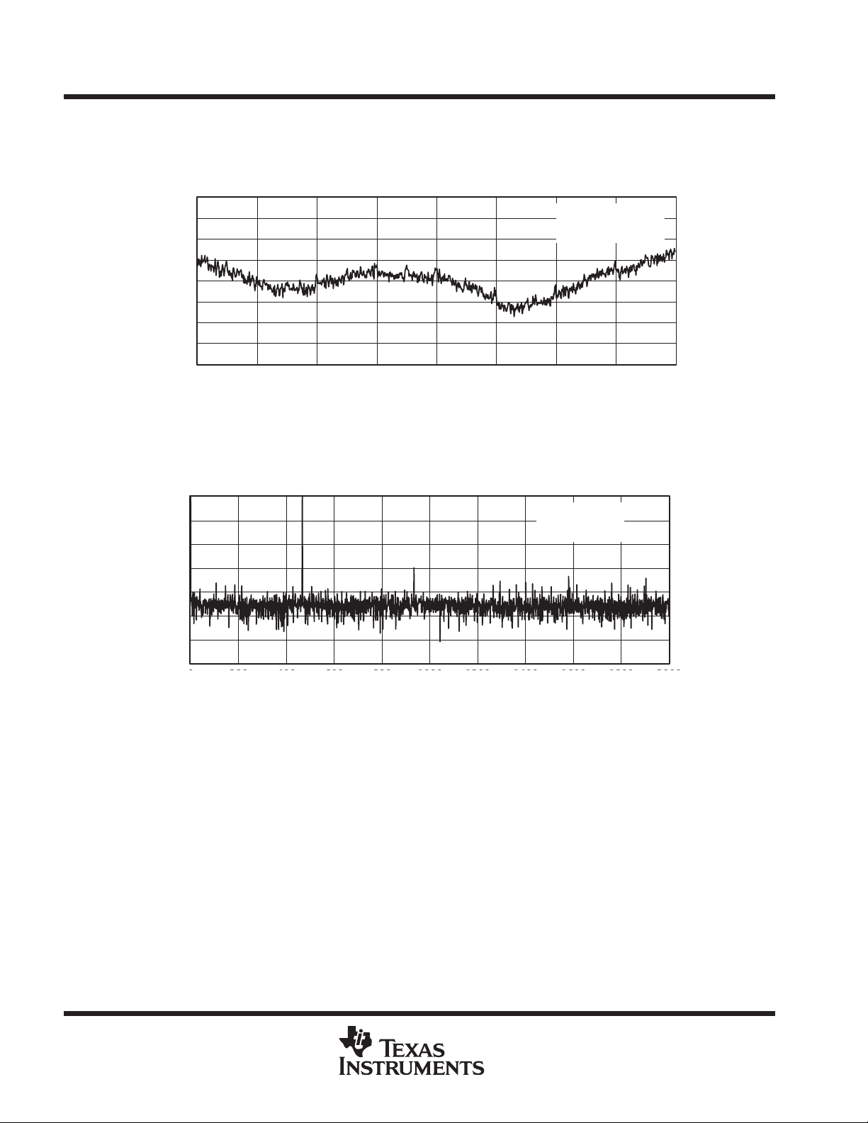
EFFECTIVE NUMBER OF BITS
FREQUENCY
10.0
9.5
9.0
8.5
8.0
7.5
Effective Number of Bits
AVDD = DVDD = 3 V
Fin = 3.5 MHz
TA = 25°C
7
5 1015202530
fs – Sampling Speed – MSPS
vs
Figure 5
EFFECTIVE NUMBER OF BITS
vs
FREQUENCY
10.0
9.5
9.0
8.5
AVDD = 5 V,
8.0
DVDD = 3 V
7.5
Effective Number of Bits
Fin = 3.5 MHz
TA = 25°C
7
5 1015202530
fs – Sampling Speed – MSPS
Figure 6
10
POST OFFICE BOX 655303 • DALLAS, TEXAS 75265

THS1031
2.7 V – 5.5 V, 10-BIT, 30 MSPS
CMOS ANALOG-TO-DIGITAL CONVERTER
SLAS242A – NOVEMBER 1999 – REVISED JANUARY 2000
TYPICAL CHARACTERISTICS
EFFECTIVE NUMBER OF BITS
vs
10.00
9.50
9.00
8.50
FREQUENCY
8.00
7.50
Effective Number of Bits
7.00
AVDD = DVDD= 5 V,
Fin = 3.5 MHz
TA = 25°C
5 1015202530
fs – Sampling Speed – MSPS
Figure 7
DIFFERENTIAL NONLINEARITY
vs
INPUT CODE
1.0
AVDD = 3 V, DVDD = 3 V
0.8
Fs = 30 MSPS
0.6
0.4
0.2
–0.0
–0.2
–0.4
–0.6
–0.8
–1
0 128 256 384 512 640 768 896 1024
DNL – Differential Nonlinearity – LSB
Input Code
Figure 8
POST OFFICE BOX 655303 • DALLAS, TEXAS 75265
11
THS1031
2.7 V – 5.5 V, 10-BIT, 30 MSPS
CMOS ANALOG-TO-DIGITAL CONVERTER
SLAS242A – NOVEMBER 1999 – REVISED JANUARY 2000
TYPICAL CHARACTERISTICS
INTEGRAL NONLINEARITY
2.0
1.5
1.0
0.5
0.0
–0.5
–1.0
–1.5
–2.0
INL – Integral Nonlinearity – LSB
0 128 256 384 512 640 768 896 1024
vs
INPUT CODE
AVDD = 3 V
DVDD = 3 V
Fs = 30 MSPS
Input Code
Figure 9
dB
FFT
vs
FREQUENCY
0
–20
–40
–60
–80
–100
–120
–140
0 200 400 600 800 1000 1200 1400 1600 1800 2000
0 1.5 3 4.5 6 7.5 9 10.5 12 13.5 15
f –Frequency – MHz
AVDD = 3 V
DVDD = 3 V
Fin = 3.5 MHz
Figure 10
12
POST OFFICE BOX 655303 • DALLAS, TEXAS 75265
Top/bottom
Center span
g
in ut
are shorted
THS1031
2.7 V – 5.5 V, 10-BIT, 30 MSPS
CMOS ANALOG-TO-DIGITAL CONVERTER
SLAS242A – NOVEMBER 1999 – REVISED JANUARY 2000
PRINCIPLES OF OPERATION
Table 1. Mode Selection
MODES ANALOG INPUT
AIN 1 V AV
p
p
External
reference
Differential
p
NOTE 1: In external reference mode, V
AIN 2 V AV
AIN 1+Ra/R
AIN External V
AIN 1 V AVDD/2 Short together 8, 14
AIN 2 V AVDD/2 AGND NC
AIN 1+Ra/R
AIN V
AIN 2 V max AGND See Note 1 See Note 1
AIN is input 1
REFTS & REFBS
together for input 2
INPUT
SPAN
b
REF
b
REF
1 V AVDD/2 Short together
2 V AVDD/2 AGND NC
V
REF
can be available for external use with CENTER SPAN setup.
REF
MODE
PIN
DD
DD
AV
DD
AVDD/2 AV
AVDD/2 Mid Ra & R
AVDD/2 AV
AVDD/2 AV
reference operations
V
-pin reference
REF
The voltage reference sources on the V
Table 2. V
REFSENSE V
AGND 2 V
AV
DD
Short to V
Connect to Ra/R
REF
The internal reference is disabled and an external reference should be connected to V
1 V
1+Ra/R
b
b
pin are controlled by the REFSENSE pin as shown in Table 2.
REF
Reference Selection
REF
REFSENSE
PIN
AGND Short together AGND 9, 16
Mid Ra & R
DD
DD
DD
VREF
PIN
Short together AGND 8, 15
Short together to R
b
External NC AGND 10, 15, 16
R
b
REF
a
External 11, 14
External
REFTS
PIN
a
Short together to the
common mode voltage
Voltage within supply
(REFTS–REBS) = 2 V max
Short together AVDD/2 17
REFBS
PIN
AGND 10, 15, 16
pin if mode = AVDD/2
REF
FIGURE
9, 14
10, 14
12, 13
POST OFFICE BOX 655303 • DALLAS, TEXAS 75265
13

THS1031
2.7 V – 5.5 V, 10-BIT, 30 MSPS
CMOS ANALOG-TO-DIGITAL CONVERTER
SLAS242A – NOVEMBER 1999 – REVISED JANUARY 2000
PRINCIPLES OF OPERATION
reference operations (continued)
D
1-V reference: The internal reference may be set to 1 V by connecting REFSENSE to V
THS1031
ADC/DAC
REF
REF
.
+
VBG
+
–
Figure 11. V
D
2-V reference: The internal reference may be set to 2 V by connecting REFSENSE to AGND.
VBG
+
–
_
REF
THS1031
+
_
1-V Reference Mode
ADC/DAC
REF
V
= 1 V
REF
REFSENSE
AGND
V
= 2 V
REF
14
Figure 12. V
POST OFFICE BOX 655303 • DALLAS, TEXAS 75265
2-V Reference Mode
REF
REFSENSE
AGND

reference operations (continued)
D
External divider: The internal reference can be set to a voltage between 1 V and 2 V by adding external
resistors.
THS1031
2.7 V – 5.5 V, 10-BIT, 30 MSPS
CMOS ANALOG-TO-DIGITAL CONVERTER
SLAS242A – NOVEMBER 1999 – REVISED JANUARY 2000
PRINCIPLES OF OPERATION
THS1031
ADC/DAC
REF
+
VBG
+
–
Figure 13. V
D
External reference: The internal reference may be overridden by using an external reference. This
_
External Divider Reference Mode
REF
condition is met by connecting REFSENSE to AVDD and an external reference circuit to the V
THS1031
ADC/DAC
REF
V
REF
= 1 + (Ra/Rb)
Ra
REFSENSE
Rb
AGND
REF
pin.
VBG
+
–
Figure 14. V
POST OFFICE BOX 655303 • DALLAS, TEXAS 75265
+
_
External Reference Mode
REF
V
= External
REF
REFSENSE
AV
DD
AGND
AGND
15

THS1031
2.7 V – 5.5 V, 10-BIT, 30 MSPS
CMOS ANALOG-TO-DIGITAL CONVERTER
SLAS242A – NOVEMBER 1999 – REVISED JANUARY 2000
PRINCIPLES OF OPERATION
reference operations (continued)
ADC reference
The MODE pin is used to select the reference source for the ADC.
D
Internal ADC Reference: Connect the MODE pin to A VDD to use the reference source for ADC generated
on the V
(REFTF+REFBF)/2 is set to a voltage for optimum operation of the ADC (near AVDD/2).
D
External ADC Reference: To supply an external reference source to the ADC, connect the MODE pin to
AGND. An external reference source should be connected to REFTF/REFTS and REFBF/REFBS.
MODE = AGND closes internal switches to allow a Kelvin connection through REFTS/REFBS, and disables
the on-chip amplifiers which drive on to the ADC references. Differential input is not supported
analog input mode
single-ended input
The single-ended input can be configured to work with either an external ADC reference or internal ADC
reference.
pin. (See V
REF
REFERENCE described in Table 2) such that (REFTF–REFBF) = V
REF
REF
and
D
External ADC Reference Mode: A single-ended analog input is accepted at the AIN pin where the input
signal is bounded by the voltages on the REFTS and REFBS pins. Figure 15 shows an example of applying
external reference to REFTS and REFBS pins in which REFTS is connected to the low-impedance 2-V
source and REFBS is connected to the low-impedance 2-V source. REFTS and REFBS may be driven to
any voltage within the supply as long as the difference (REFTS – REFBS) is between 1 V and 2 V as
specified in Table 2. Figure 16 shows an example of external-reference using a Kelvin connection to
eliminate line voltage drop errors.
2 V
1 V
2 V
1 V
0.1 µF
AIN
REFTS
REFBS
MODE
SW3
REFTF
10 µF0.1 µF
THS1031
SHA
PGA
A/D
16
REFBF
0.1 µF
Figure 15. External ADC Reference Mode
POST OFFICE BOX 655303 • DALLAS, TEXAS 75265

analog input mode(continued)
THS1031
2.7 V – 5.5 V, 10-BIT, 30 MSPS
CMOS ANALOG-TO-DIGITAL CONVERTER
SLAS242A – NOVEMBER 1999 – REVISED JANUARY 2000
PRINCIPLES OF OPERATION
REFT
REFB
0.1
µF
0.1 µF
REFTF
REFBF
0.1 µF
0.1 µF
0.1 µF
AIN
REFTS
REFBS
MODE
SW3
REFTF
10 µF
REFBF
THS1031
SHA A/DPGA
Figure 16. Kelvin Connection With External ADC Reference Mode
D
Internal ADC Reference Mode With External Input Common Mode: The input common mode is supplied
to pins REFTS and REFBS while connected together. The input signal should be centered around this
common mode with peak-to-peak input equal to the voltage on the V
pin. Input can be either dc-coupled
REF
or ac-coupled to the same common mode voltage (Figure 17) or any other voltage within the input voltage
range.
2 V
1 V
1.5 V
AV
DD
AIN
REFTS
REFBS
MODE
V
REF
REFSENSE
THS1031
SHA
+
_
+–
1 V
PGA
ADC
REF
Figure 17. External Input Common Mode
POST OFFICE BOX 655303 • DALLAS, TEXAS 75265
A/D
REFTF
0.1 µF
REFBF
0.1 µF
10 µF
0.1 µF
17

THS1031
2.7 V – 5.5 V, 10-BIT, 30 MSPS
CMOS ANALOG-TO-DIGITAL CONVERTER
SLAS242A – NOVEMBER 1999 – REVISED JANUARY 2000
PRINCIPLES OF OPERATION
analog input mode(continued)
D
Internal ADC Reference Mode With Common Mode Input V
V
/2 by connecting REFTS to V
REF
and AVSS.
and REFBS to AVSS. The input signal at AIN will swing between V
REF
/2: The input common mode is set to
REF
REF
1.5 V
2 V
0 V
2 V
1 V
AV
AIN
REFTS
REFBS
DD
MODE
V
REF
REFSENSE
Figure 18. Common Mode Input V
AIN
REFTS
THS1031
SHA A/DPGA
A/D
REFTF
0.1 µF
REFBF
0.1 µF
10 µF
0.1 µF
ADC
REF
+
_
+–
1 V
/2 With 1-V Internal Reference
REF
THS1031
SHA
PGA
18
AV
DD
REFBS
MODE
V
REF
REFSENSE
+
_
Figure 19. Common Mode Input V
POST OFFICE BOX 655303 • DALLAS, TEXAS 75265
ADC
REF
+–
1 V
/2 With 2-V Internal Reference
REF
REFTF
0.1 µF
REFBF
0.1 µF
10 µF
0.1 µF
2.7 V – 5.5 V, 10-BIT, 30 MSPS
CMOS ANALOG-TO-DIGITAL CONVERTER
SLAS242A – NOVEMBER 1999 – REVISED JANUARY 2000
PRINCIPLES OF OPERATION
analog input mode(continued)
differential input
In this mode, the first differential input is applied to the AIN pin and the second differential input is applied to the
common point where REFTS and REFBS are tied together. The common mode of the input should be set to
AVDD/2 as shown in Figure 20. The maximum magnitude of the differential input signal should be equal to V
V
REF
THS1031
AIN
AVDD/2
REFTS
REFBS
SHA
PGA
A/D
THS1031
REF
.
DD
MODE
V
REF
V
is either internal or external
REF
ADC
REF
REFTF
0.1 µF
REFBF
0.1 µF
10 µF
0.1 µF
AV
Figure 20. Differential Input
digital input mode
The THS1031 contains 4 registers: two CLAMP registers, a CONTROL register, and a TEST register . The TEST
register is reserved for test purposes. Binary data can be written into the CLAMP and CONTROL registers via
I/O0–I/O9 by inserting an active-low write strobe to the WR input pin and an active-low signal to the OE input
pin. This will disable the ADC’s output bus. The two MSBs of each register are address bits. For example, set
bit 9 and bit 8 to 00 to select the clamp register 1. Set bit 9 and bit 8 to 01 to select the clamp register 2.
clamp registers
The internal digital clamp circuit uses a 10-bit DAC to convert the 10-bit digital value into the analog clamp level
in which the clamp register 1 contains 8 LSBs of DAC(7:0). The clamp register 2 contains two MSBs of the
DAC(9:8). DAC(9:8)
into 4 quarters which can be selected by bit 0 (DAC8) and bit 1 (DAC9) in the clamp register 2. The user can
clamp to any of 256-dc levels within each quarter determined by the 8-bit content of the clamp register 1.
Figure 21 shows how the DACs 10-bit digital input map to the analog clamping range from 0 V to V
D
Clamp Register 1
9 8 7 6 5 4 3 2 1 0
0 0 DAC7 DAC6 DAC5 DAC4 DAC3 DAC2 DAC1 DAC0
(Default = 00):
For clamping purpose, the entire range of voltage reference V
REF
is divided
.
REF
D
Clamp Register 2
9 8 7 6 5 4 3 2 1 0
0 1 X X X X X X DAC9 DAC8
POST OFFICE BOX 655303 • DALLAS, TEXAS 75265
19

THS1031
2.7 V – 5.5 V, 10-BIT, 30 MSPS
CMOS ANALOG-TO-DIGITAL CONVERTER
SLAS242A – NOVEMBER 1999 – REVISED JANUARY 2000
PRINCIPLES OF OPERATION
digital input mode (continued)
REFTF
3/4 (REFTF – REFBF)
1/2 (REFTF – REFBF)
1/4 (REFTF – REFBF)
REFBF
DAC (9:0)
1111111111
•
•
•
1100000000
1011111111
•
•
•
1000000000
0111111111
•
•
•
0100000000
0011111111
•
•
•
0000000000
Figure 21. Digital Clamp Input Range
control register
9 8 7 6 5 4 3 2 1 0
1 0 X Clamp Disable Bin/2’s Output INT/EXT Clamp Power Down PGA2 PGA1 PGA0
D
Clamp Disable
D
BIN/2s Output:
set bit 5 to1 to set the output data format to 2s complement.
D
INT/EXT Clamp: (
or set bit 4 to 1 to select the internal digital clamp whose clamp level is defined in the clamp register
described above.
D
Power Down: (
: (Default = 0)
Set bit 6 to 1 to disable the internal clamp amplifier for power savings.
(Default is straight binary
Default = 0)
Default = 0)
Set bit 4 of the CONTROL register to 0 to select the external analog clamp
Set bit 3 of the CONTROL register to 1 to power down the THS1031.
) Set bit 5 to 0 to set the output data format to straight binary or
20
POST OFFICE BOX 655303 • DALLAS, TEXAS 75265

digital input mode (continued)
D
PGA(2–0): (
table:
test register (reserved)
9 8 7 6 5 4 3 2 1 0
1 1 X X X X X X X X
Default = 001)
THS1031
2.7 V – 5.5 V, 10-BIT, 30 MSPS
CMOS ANALOG-TO-DIGITAL CONVERTER
SLAS242A – NOVEMBER 1999 – REVISED JANUARY 2000
PRINCIPLES OF OPERATION
3-bit gain for programmable gain amplifier can be set as indicated in the following
PGA[2–0] GAIN
000 0.5
001 Unity gain
010 1.5
011 2.0
100 2.5
101 3.0
110 3.5
111 4.0
digital output mode
D
3-State Output: The digital outputs can be set to high-impedance state by applying a Hi logic to the OE
pin.
D
Output Format: Defined by bit 5 of the CONTROL register. The output format is straight binary if bit 5 set
to 0. The output format is 2s complement if bit 5 is set to 1.
The default format is straight binary
clamp operation
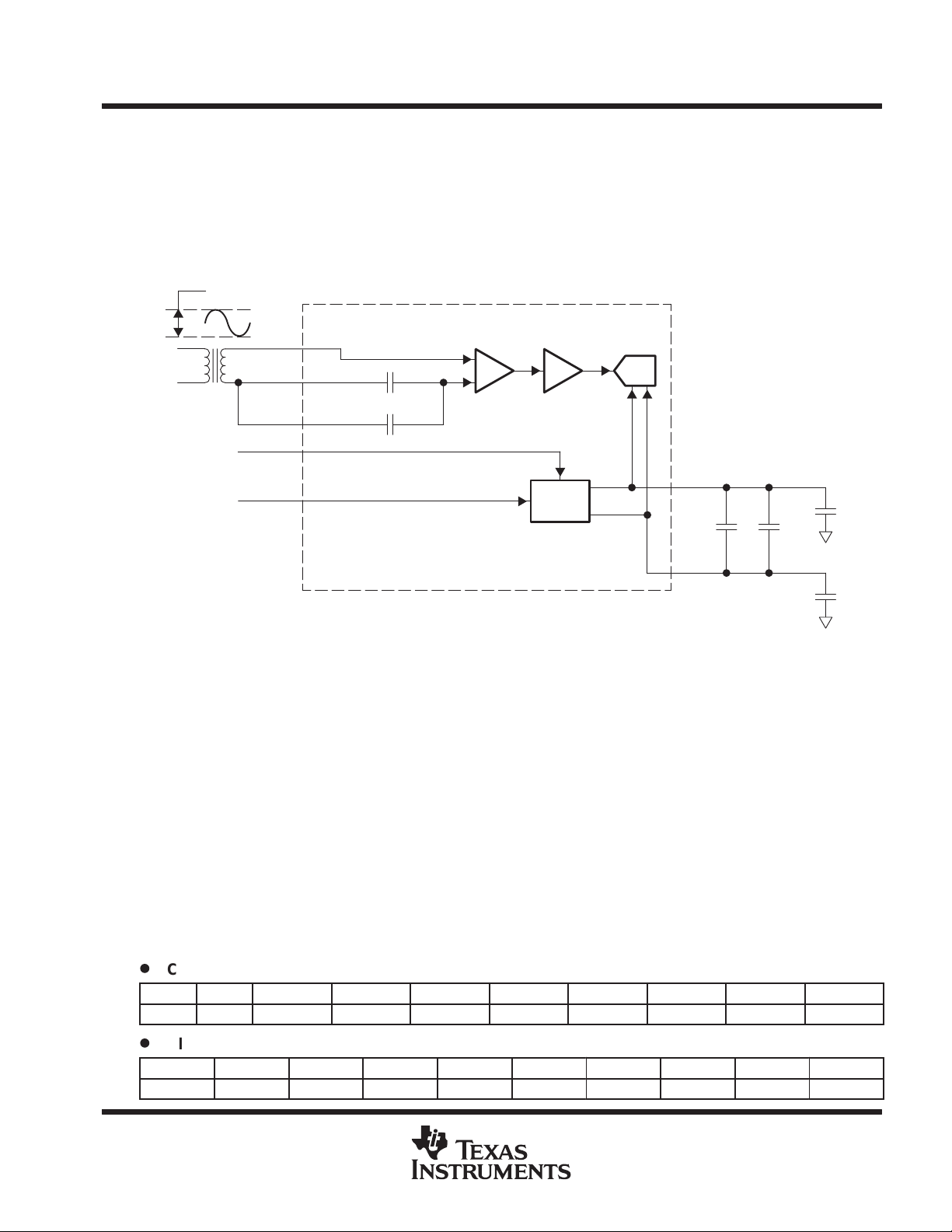
The THS1031 ADC features an internal clamp circuit for dc restoration of video or ac coupled signals. The clamp
input level can come from either an external source or an internal digital clamp circuit containing a 10-bit DAC
and clamp register.
D
External Clamp Input: To enable the external clamp input source, use the default state on power up or
write a 0 to bit 4 of the PGA/CONTROL register. This will connect the switch SW2 to the CLAMPIN pin. The
clamp amplifier will then servo the voltage at the AIN pin to be equal to the clamp voltage applied at the
CLAMPIN pin. After the desired clamp level is attained, the switch SW1 is opened by taking CLAMP back
to logic low. Ignoring the droop caused by the input bias current, the input capacitor CIN will hold the DC
voltage at AIN constant until the next clamp interval. The input resistor RIN has a minimum recommended
value of 10 W, to maintain the closed-loop stability of the clamp amplifier.
D
Internal Programmable Digital Clamp Input: The THS1031 ADC features a programmable digital clamp
circuit to set more precise clamping level to 1-LSB accuracy for dc restoration of video or ac coupled signals.
Figure 22 shows the internal clamp circuitry and the external control signals needed for the digital clamp
operation. To enable the digital clamp input source, write a 1 to bit 4 of the CONTROL register which will
connect the switch SW2 to the output of the 10-bit clamp DAC. In the CLAMP register, bit 0 to bit 7 are used
to set the clamp level input to the 10-bit DAC and bit 6–7 are used to select one of 4 equal clamping voltage
sub-ranges as described in the description of CLAMP REGISTER for digital input mode. The clamp
amplifier will then servo the voltage at the AIN pin to be equal to the clamp voltage applied at the CLAMPIN
pin. After the desired clamp level is attained, the switch SW1 is opened by taking CLAMP back to logic low.
Ignoring the droop caused by the input bias current, the input capacitor CIN will hold the dc voltage at AIN
constant until the next clamp interval. The input resistor RIN has a minimum recommended value of 10 W,
to maintain the closed-loop stability of the clamp amplifier.
.
POST OFFICE BOX 655303 • DALLAS, TEXAS 75265
21

THS1031
2.7 V – 5.5 V, 10-BIT, 30 MSPS
CMOS ANALOG-TO-DIGITAL CONVERTER
SLAS242A – NOVEMBER 1999 – REVISED JANUARY 2000
PRINCIPLES OF OPERATION
clamp operation (continued)
D
Clamp and Droop Analysis
16–Bit DAC
Control
Register
C1
CLAMPIN
CLAMP
R1
AIN
SW1
SW2
+
–
S/H
Figure 22. Clamp Operation
D
Clamp Acquisition Time: Figure 22 shows the basic operation of the clamp circuit in which the ac input
signal is passed through an RC coupler.
The acquisition time when the switch is closed will equal a: T(acq) = Ci.Ri ln(Vc/Ve)(Eq.1)
In case of composite video, typical input Ri = 20 Ω. In a video clamping application, the droop is a critical
parameter and thus the input capacitor should be sized to allow sufficient acquisition time of clamp voltage at
AIN within the CLAMP interval, but also to minimize droop between clamping intervals. Typically, Ci = 1µF
By applying equation 1 above, the following examples apply to an NTSC composite video signal:
D
The acquisition time needed to clamp 1-V input level to black level (0.340 Vdc ) is about 130 µs.
D
The acquisition time needed to clamp 2-V input level to the white level (1 Vdc) is about 140 µs.
D
The acquisition time needed to clamp 3-V input level to the sync level (0.288 Vdc) is about 160 µs.
droop
The voltage droop is the voltage change across the input capacitor C
dV
+ǒI
ń
CiǓ(t)
bias
by the bias current as follows:
i
where t = elapsed time between clamping intervals
The bias current depends on the sampling rate. For a sampling rate of 30 MSPS and a typical input capacitance
of 1 pF, the input resistance is
Rs = 1/(Cs.Fs) = 1/(1 pFx30 MHz) = 33 kΩ
For 1-V input range and clamping period = 64 µs, the max bias current will equal I
= 0.5 V/33 kΩ = 15 µA:
bias
dV = (15 µA/1 µF)(64 µs) = 0.96 mV
For 1-V input range and clamping period = 64 µs, the max bias current will equal I
= 0.5 V/33 kΩ = 15 µA:
bias
dV = (15 µA/1 µF)(64 µs) = 0.96 mV
For 2-V input range and clamping period = 64 µs, the max bias current will equal I
= 1.0 V/33 kΩ = 30 µA
bias
dV = (30 µA/1 µF)(64 µs) = 1.9 mV
22
POST OFFICE BOX 655303 • DALLAS, TEXAS 75265

2.7 V – 5.5 V, 10-BIT, 30 MSPS
CMOS ANALOG-TO-DIGITAL CONVERTER
SLAS242A – NOVEMBER 1999 – REVISED JANUARY 2000
PRINCIPLES OF OPERATION
clamp operation (continued)
requirements
For a single direct source of NTSC video,
D
The initial clamp acquisition time needs to be between 130 µs and 160 µs to set the input dc level within
1 mV accuracy.
D
The clamp pulse at CLAMP is recommended to be 2 µs (typ).
D
The droop voltage needs to be compensated within one clamping period of 64 µs for 1 V and 2 V. Input
ranges are 1 mV and 1.9 mV respectively which are less than 1 LSB.
power management
Upon power up, the THS1031 is put in the default mode. In the default mode, the PGA (PGA bypass) and the
clamp DAC are powered down which adds to the device’s flexibility. The users need not incur the penalty of
having to provide power for a certain section if it is not necessary to their design.
When bit 3 of PGA/control register is set to 1, the entire device is powered down. The ADC will wake-up in 400 ns
(typ) after the bit 3 is reset.
THS1031
POST OFFICE BOX 655303 • DALLAS, TEXAS 75265
23

THS1031
2.7 V – 5.5 V, 10-BIT, 30 MSPS
CMOS ANALOG-TO-DIGITAL CONVERTER
SLAS242A – NOVEMBER 1999 – REVISED JANUARY 2000
MECHANICAL DATA
PW (R-PDSO-G**) PLASTIC SMALL-OUTLINE
14 PINS SHOWN
0,65
1,20 MAX
14
0,30
0,19
8
4,50
4,30
PINS **
7
Seating Plane
0,15
0,05
8
1
A
DIM
14
0,10
6,60
6,20
M
0,10
0,15 NOM
2016
0°–8°
Gage Plane
24
0,25
0,75
0,50
28
A MAX
A MIN
NOTES: A. All linear dimensions are in millimeters.
B. This drawing is subject to change without notice.
C. Body dimensions do not include mold flash or protrusion not to exceed 0,15.
D. Falls within JEDEC MO-153
3,10
2,90
5,10
4,90
5,10
4,90
6,60
6,40
7,90
7,70
9,80
9,60
4040064/F 01/97
24
POST OFFICE BOX 655303 • DALLAS, TEXAS 75265

THS1031
2.7 V – 5.5 V, 10-BIT, 30 MSPS
CMOS ANALOG-TO-DIGITAL CONVERTER
SLAS242A – NOVEMBER 1999 – REVISED JANUARY 2000
MECHANICAL DATA
DW (R-PDSO-G**) PLASTIC SMALL-OUTLINE
16 PINS SHOWN
0.050 (1,27)
16
1
0.020 (0,51)
0.014 (0,35)
9
0.299 (7,59)
0.293 (7,45)
8
A
0.010 (0,25)
0.419 (10,65)
0.400 (10,15)
M
0.010 (0,25) NOM
0°–8°
Gage Plane
0.010 (0,25)
0.050 (1,27)
0.016 (0,40)
0.104 (2,65) MAX
NOTES: A. All linear dimensions are in inches (millimeters).
B. This drawing is subject to change without notice.
C. Body dimensions do not include mold flash or protrusion not to exceed 0.006 (0,15).
D. Falls within JEDEC MS-013
0.012 (0,30)
0.004 (0,10)
DIM
A MAX
A MIN
PINS **
16
0.410
(10,41)
0.400
(10,16)
Seating Plane
0.004 (0,10)
20
0.510
(12,95)
0.500
(12,70)
24
0.610
(15,49)
0.600
(15,24)
28
0.710
(18,03)
0.700
(17,78)
4040000/C 07/96
POST OFFICE BOX 655303 • DALLAS, TEXAS 75265
25

IMPORTANT NOTICE
T exas Instruments and its subsidiaries (TI) reserve the right to make changes to their products or to discontinue
any product or service without notice, and advise customers to obtain the latest version of relevant information
to verify, before placing orders, that information being relied on is current and complete. All products are sold
subject to the terms and conditions of sale supplied at the time of order acknowledgement, including those
pertaining to warranty, patent infringement, and limitation of liability.
TI warrants performance of its semiconductor products to the specifications applicable at the time of sale in
accordance with TI’s standard warranty. Testing and other quality control techniques are utilized to the extent
TI deems necessary to support this warranty . Specific testing of all parameters of each device is not necessarily
performed, except those mandated by government requirements.
CERTAIN APPLICATIONS USING SEMICONDUCTOR PRODUCTS MAY INVOLVE POTENTIAL RISKS OF
DEATH, PERSONAL INJURY, OR SEVERE PROPERTY OR ENVIRONMENTAL DAMAGE (“CRITICAL
APPLICATIONS”). TI SEMICONDUCTOR PRODUCTS ARE NOT DESIGNED, AUTHORIZED, OR
WARRANTED TO BE SUITABLE FOR USE IN LIFE-SUPPORT DEVICES OR SYSTEMS OR OTHER
CRITICAL APPLICA TIONS. INCLUSION OF TI PRODUCTS IN SUCH APPLICATIONS IS UNDERST OOD TO
BE FULLY AT THE CUSTOMER’S RISK.
In order to minimize risks associated with the customer’s applications, adequate design and operating
safeguards must be provided by the customer to minimize inherent or procedural hazards.
TI assumes no liability for applications assistance or customer product design. TI does not warrant or represent
that any license, either express or implied, is granted under any patent right, copyright, mask work right, or other
intellectual property right of TI covering or relating to any combination, machine, or process in which such
semiconductor products or services might be or are used. TI’s publication of information regarding any third
party’s products or services does not constitute TI’s approval, warranty or endorsement thereof.
Copyright 2000, Texas Instruments Incorporated
 Loading...