

T
查询THS1030供应商
THS1030
2.7 V – 5.5 V, 10-BIT, 30 MSPS
CMOS ANALOG-TO-DIGITAL CONVERTER
SLAS243A – NOVEMBER 1999 – REVISED JANUARY 2000
D
10-Bit Resolution 30 MSPS
Analog-to-Digital Converter:
D
Configurable Input: Single-Ended or
Differential
D
Differential Nonlinearity: ±0.3 LSB
D
Signal-to-Noise: 57 dB
D
Spurious Free Dynamic Range: 60 dB
D
Adjustable Internal Voltage Reference
D
Out-of-Range Indicator
D
Power-Down Mode
D
Pin Compatible with TLC876
description
The THS1030 is a CMOS, low power, 10-bit, 30
MSPS analog-to-digital converter (ADC) that can
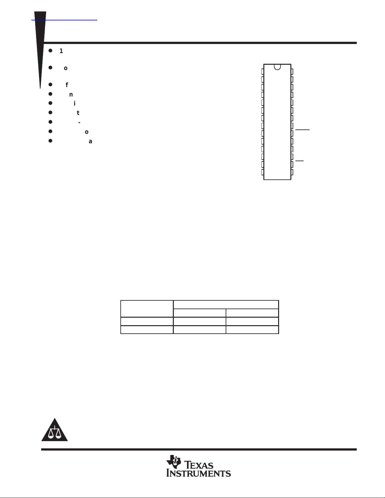
28-PIN TSSOP/SOIC PACKAGE
AGND
DV
DGND
DD
I/O0
I/O1
I/O2
I/O3
I/O4
I/O5
I/O6
I/O7
I/O8
I/O9
OVR
(TOP VIEW)
1
28
2
27
3
26
4
25
5
24
6
23
7
22
8
21
9
20
10
19
11
18
12
17
13
16
14
15
AV
DD
AIN
V
REF
REFBS
REFBF
MODE
REFTF
REFTS
876M
AGND
REFSENSE
STBY
OE
CLK
operate with a supply range from 2.7 V to 3.3 V.
The THS1030 has been designed to give circuit
developers more flexibility . The analog input to the
THS1030 can be either single-ended or differential. The THS1030 provides a wide selection of voltage
references to match the user’s design requirements. For more design flexibility, the internal reference can be
bypassed to use an external reference to suit the dc accuracy and temperature drift requirements of the
application. The out-of-range output is used to monitor any out-of-range condition in THS1030s input range.
The speed, resolution, and single-supply operation of the THS1030 are suited for applications in STB, video,
multimedia, imaging, high-speed acquisition, and communications. The speed and resolution ideally suit
charge-couple device (CCD) input systems such as color scanners, digital copiers, digital cameras, and
camcorders. A wide input voltage range between REFBS and REFTS allows the THS1030 to be applied in both
imaging and communications systems.
The THS1030I is characterized for operation from –40°C to 85°C
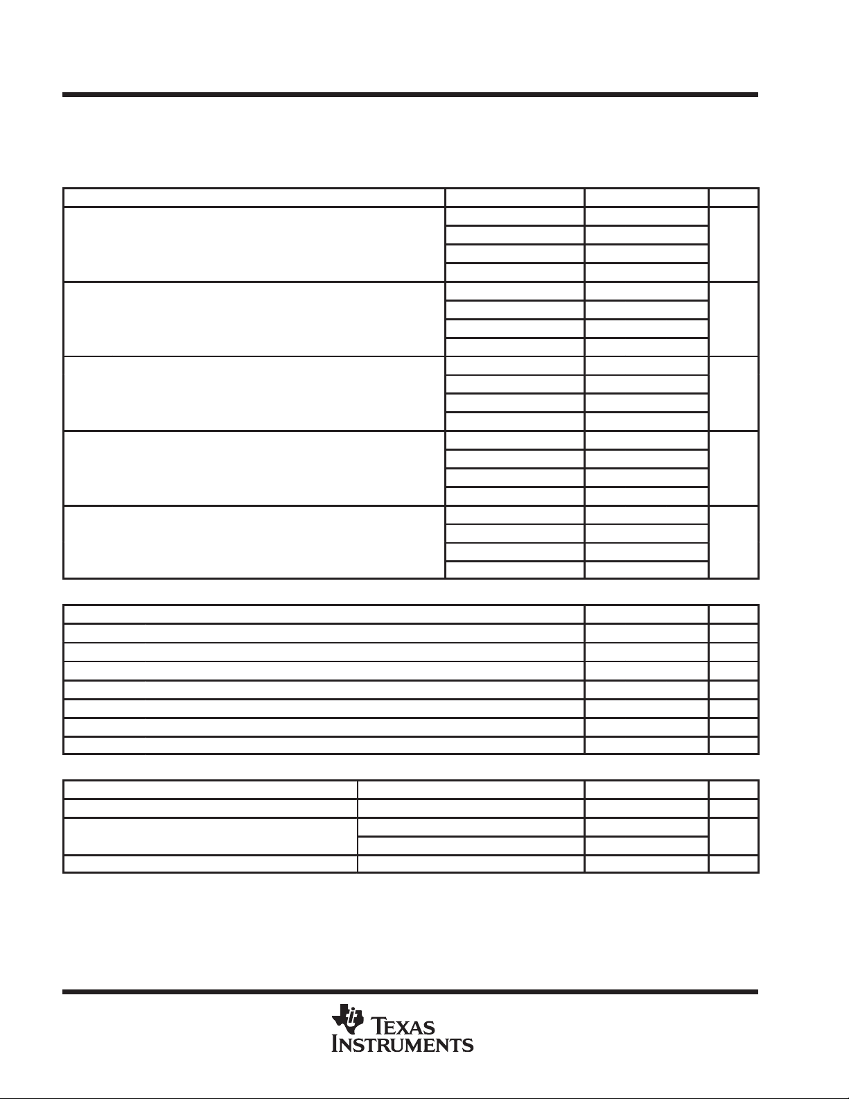
AVAILABLE OPTIONS
A
0°C to 70°C THS1030CPW THS1030CDW
–40°C to 85°C THS1030IPW THS1030IDW
28-TSSOP (PW) 28-SOIC (DW)
PACKAGED DEVICES
Please be aware that an important notice concerning availability, standard warranty, and use in critical applications of
Texas Instruments semiconductor products and disclaimers thereto appears at the end of this data sheet.
TI is a trademark of Texas Instruments Incorporated.
PRODUCTION DATA information is current as of publication date.
Products conform to specifications per the terms of Texas Instruments
standard warranty. Production processing does not necessarily include
testing of all parameters.
POST OFFICE BOX 655303 • DALLAS, TEXAS 75265
Copyright 2000, Texas Instruments Incorporated
1
THS1030
2.7 V – 5.5 V, 10-BIT, 30 MSPS
CMOS ANALOG-TO-DIGITAL CONVERTER
SLAS243A – NOVEMBER 1999 – REVISED JANUARY 2000
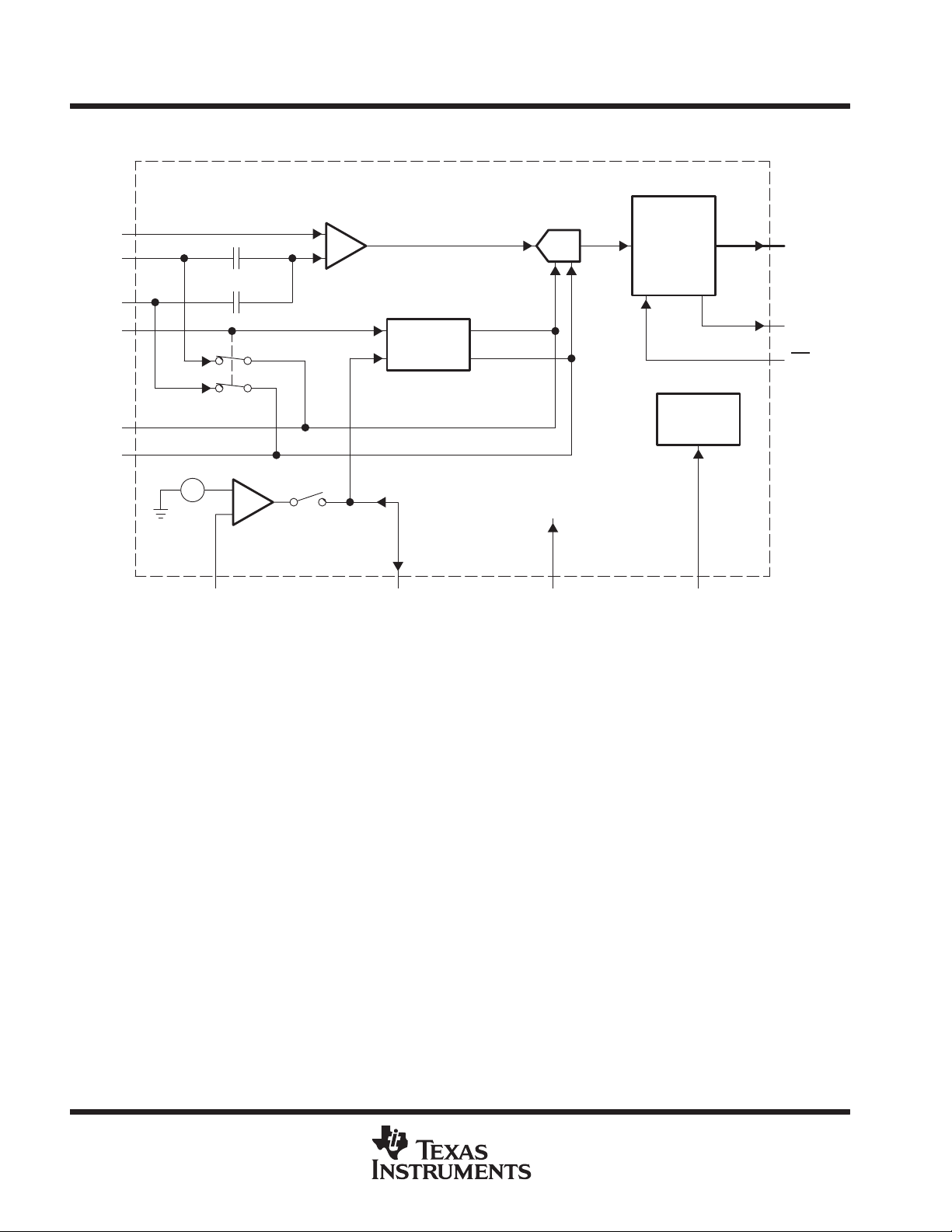
functional block diagram
AIN
REFTS
REFBS
MODE
REFTF
REFBF
SHA
DC
REF
SW3
VBG
SW4
REFSENSE VREF CLK
A/D
STBY
Output
Buffers
Timing
Circuit
I/O0 –
I/O9
OVR
OE
2
POST OFFICE BOX 655303 • DALLAS, TEXAS 75265
I/O
DESCRIPTION
2.7 V – 5.5 V, 10-BIT, 30 MSPS
CMOS ANALOG-TO-DIGITAL CONVERTER
SLAS243A – NOVEMBER 1999 – REVISED JANUARY 2000
Terminal Functions
TERMINAL
NAME NO.
AGND 1, 19 I Analog ground
AIN 27 I Analog input
AV
DD
CLK 15 I Clock input
DGND 14 I Digital ground
DV
DD
I/O0
I/O1
I/O2
I/O3
I/O4
I/O5
I/O6
I/O7
I/O8
I/O9
MODE 23 I Mode input
OE 16 I HI to the 3-state data bus, LO to enable the data bus
OVR 13 O Out-of-range indicator
REFBS 25 I Reference bottom sense
REFBF 24 I Reference bottom decoupling
REFSENSE 18 I Reference sense
REFTF 22 I Reference top decoupling
REFTS 21 I Reference top sense
STBY 17 I HI = power down mode, LO = normal operation mode
V
REF
876M 20 I HI = THS1030 mode, LO = TLC876 mode (see section 4 for TLC876 mode)
28 I Analog supply
2 I Digital driver supply
3
4
5
6
7
8
9
10
11
12
26 I/O Internal and external reference for ADC
Digital I/O bit 0 (LSB)
Digital I/O bit 1
Digital I/O bit 2
Digital I/O bit 3
Digital I/O bit 4
I/O
Digital I/O bit 5
Digital I/O bit 6
Digital I/O bit 7
Digital I/O bit 8
Digital I/O bit 9 (MSB)
THS1030
POST OFFICE BOX 655303 • DALLAS, TEXAS 75265
3

THS1030
Suppl
oltage
Maximum sampling rate
MSPS
V
2.7 V – 5.5 V, 10-BIT, 30 MSPS
CMOS ANALOG-TO-DIGITAL CONVERTER
SLAS243A – NOVEMBER 1999 – REVISED JANUARY 2000
absolute maximum ratings over operating free-air temperature (unless otherwise noted)
†
Supply voltage: AVDD to AGND, DVDD to DGND –0.3 to 6.5 V. . . . . . . . . . . . . . . . . . . . . . . . . . . . . . . . . . . . . .
AGND to DGND –0.3 to 0.3 V. . . . . . . . . . . . . . . . . . . . . . . . . . . . . . . . . . . . . . . . . . . . . . . . . . . . .
AV
to DVDD –6.5 to 6.5 V. . . . . . . . . . . . . . . . . . . . . . . . . . . . . . . . . . . . . . . . . . . . . . . . . . . . . .
DD
Mode input MODE to AGND –0.3 to AVDD + 0.3 V. . . . . . . . . . . . . . . . . . . . . . . . . . . . . . . . . . . . . . . . . . . . . . . . . .
Reference voltage input range REFTF, REFTB, REFTS, REFBS to AGND –0.3 to AVDD + 0.3 V. . . . . . . . .
Analog input voltage range AIN to AGND –0.3 to AVDD + 0.3 V. . . . . . . . . . . . . . . . . . . . . . . . . . . . . . . . . . . . . .
Reference input V
Reference output V
to AGND –0.3 to AVDD + 0.3 V. . . . . . . . . . . . . . . . . . . . . . . . . . . . . . . . . . . . . . . . . . . . . .
REF
to AGND –0.3 to AVDD + 0.3 V. . . . . . . . . . . . . . . . . . . . . . . . . . . . . . . . . . . . . . . . . . . . .
REF
Clock input CLK to AGND –0.3 to AVDD + 0.3 V. . . . . . . . . . . . . . . . . . . . . . . . . . . . . . . . . . . . . . . . . . . . . . . . . . . .
Digital input to DGND –0.3 to DVDD + 0.3 V. . . . . . . . . . . . . . . . . . . . . . . . . . . . . . . . . . . . . . . . . . . . . . . . . . . . . . . .
Digital output to DGND –0.3 to DVDD + 0.3 V. . . . . . . . . . . . . . . . . . . . . . . . . . . . . . . . . . . . . . . . . . . . . . . . . . . . . .
Operating junction temperature range, T
Storage temperature range, T
–65°C to 150°C. . . . . . . . . . . . . . . . . . . . . . . . . . . . . . . . . . . . . . . . . . . . . . . . .
STG
0°C to 150°C. . . . . . . . . . . . . . . . . . . . . . . . . . . . . . . . . . . . . . . . . . . . .
J
Lead temperature 1,6 mm (1/16 in) from case for 10 seconds 300°C. . . . . . . . . . . . . . . . . . . . . . . . . . . . . . . . . .
†
Stresses beyond those listed under “absolute maximum ratings” may cause permanent damage to the device. These are stress ratings only, and
functional operation of the device at these or any other conditions beyond those indicated under “recommended operating conditions” is not
implied. Exposure to absolute-maximum-rated conditions for extended periods may affect device reliability.
recommended operating conditions
digital inputs
MIN NOM MAX UNIT
High-level input voltage, V
Low-level input voltage, V
IH
IL
analog inputs
Analog input voltage, V
Reference input voltage, V
Reference input voltage, V
Reference input voltage, V
I(AIN)
I(VREF)
I(REFTS)
I(REFBS)
power supply
AV
pp
y v
p
= 30
DV
DD
DD
REFTS, REFBS reference voltages (MODE = AVDD)
PARAMETER MIN NOM MAX UNIT
REFTS Reference input voltage (top) 1 AV
REFBS Reference input voltage (bottom) 0 AVDD–1 V
Differential input (REFTS – REFBS) 1 2 V
Switched input capacitance on REFTS 0.5 pF
2.4 V
0.2 x DV
MIN NOM MAX UNIT
REFBS REFTS V
1 2 V
1 AV
0 AVDD–1 V
MIN NOM MAX UNIT
2.7 3 5.5
2.7 3 5.5
DD
DD
DD
V
V
V
sampling rate and resolution
Fs 5 30 MSPS
Resolution 10 Bits
4
PARAMETER MIN NOM MAX UNIT
POST OFFICE BOX 655303 • DALLAS, TEXAS 75265
Input common mode (REFTF
REFBF)/2
V
V
1 V
V
REFTF (MODE
AVDD)
V
V
V
V
V
V
REFBF (MODE
AVDD)
V
2 V
V
THS1030
2.7 V – 5.5 V, 10-BIT, 30 MSPS
CMOS ANALOG-TO-DIGITAL CONVERTER
SLAS243A – NOVEMBER 1999 – REVISED JANUARY 2000
electrical characteristics over recommended operating conditions, A VDD = 3 V , DVDD = 3 V , Fs = 30
MSPS/50% duty cycle, MODE = AV
–40°C to 85°C (unless otherwise noted)
analog inputs
PARAMETER MIN TYP MAX UNIT
V
I(AIN)
C
I
FPBW Full power BW (–3 dB) 150 MHz
VREF reference voltages
REFTF, REFBF reference voltages
Differential input (REFTF – REFBF) 1 2 V
p
Input resistance between REFTF and REFBF 600 Ω
Analog input voltage REFBS REFTS V
Switched input capacitance 1.2 pF
DC leakage current (input = ±FS) 60 µA
PARAMETER MIN TYP MAX UNIT
Internal 1 V reference (REFSENSE = V
Internal 2 V reference (REFSENSE = AVSS) 1.90 2 2.10 V
External reference (REFSENSE = AVDD) 1 2 V
Reference input resistance 18 kΩ
PARAMETER TEST CONDITIONS MIN TYP MAX UNIT
+
=
=
, 2 V input span from 0.5 V to 2.5 V, external reference, TA =
DD
) 0.95 1 1.05 V
REF
AVDD = 3 V 1.3 1.5 1.7
AVDD = 5 V 2 2.5 3
REF
REF
REF
REF
=
= 2
= 1
=
AVDD = 3 V 2
AVDD = 5 V 3
AVDD = 3 V 2.5
AVDD = 5 V 3.5
AVDD = 3 V 1
AVDD = 5 V 0.5
AVDD = 3 V 2
AVDD = 5 V 1.5
dc accuracy
INL Integral nonlinearity ±1 ±2 LSB
DNL Differential nonlinearity ±0.3 ±1 LSB
PARAMETER MIN TYP MAX UNIT
Offset error 0.4 1.4 %FSR
Gain error 1.4 3.5 %FSR
Missing code No missing code assured
POST OFFICE BOX 655303 • DALLAS, TEXAS 75265
5
THS1030
ENOB
Effective number of bits
Bits
SFDR
Spurious free dynamic range
THD
Total harmonic distortion
dB
SNR
Signal-to-noise
SINAD
Signal-to-noise and distortion
dB
PDPower dissipation
mW
2.7 V – 5.5 V, 10-BIT, 30 MSPS
CMOS ANALOG-TO-DIGITAL CONVERTER
SLAS243A – NOVEMBER 1999 – REVISED JANUARY 2000
electrical characteristics over recommended operating conditions, A VDD = 3 V , DVDD = 3 V , Fs = 30
MSPS/50% duty cycle, MODE = AV
–40°C to 85°C (unless otherwise noted) (continued)
dynamic performance
PARAMETER TEST CONDITIONS MIN TYP MAX UNIT
p
, 2 V input span from 0.5 V to 2.5 V, external reference, TA =
DD
f = 3.5 MHz 8.4 9
f = 3.5 MHz, AVDD = 5 V 9
f = 15 MHz, 3 V 7.8
f = 15 MHz, AVDD = 5 V 7.7
f = 3.5 MHz 56 60.6
f = 3.5 MHz, AVDD = 5 V 64.6
f = 15 MHz 48.5
f = 15 MHz, AVDD = 5 V 53
f = 3.5 MHz –60 –56
f = 3.5 MHz, AVDD = 5 V –66.9
f = 15 MHz –47.5
f = 15 MHz, AVDD = 5 V –53.1
f = 3.5 MHz 53 57
f = 3.5 MHz, AVDD = 5 V 56
f = 15 MHz 53.1
f = 15 MHz, AVDD = 5 V 49.4
f = 3.5 MHz 52.5 56
f = 3.5 MHz, AVDD = 5 V 56
f = 15 MHz 48.6
f = 15 MHz, AVDD = 5 V 48.1
dB
dB
clock
PARAMETER MIN TYP MAX UNIT
t
(CK)
t
(CKH)
t
(CKL)
t
d
t
(ap)
Clock period 33 ns
Pulse duration, clock high 15 16.5 ns
Pulse duration, clock low 15 16.5 ns
Clock to data valid 20 ns
Pipeline latency 3 Cycles
Aperture delay 4 ns
Aperture uncertainty (jitter) 2 ps
power supply
PARAMETER TEST CONDITIONS MIN TYP MAX UNIT
I
CC
PD(STBY) Standby power AVDD =DVDD = 3 V, MODE = AGND 3 5 mW
Operating supply current AVDD =DVDD = 3 V, MODE = AGND 29 40 mA
p
AVDD = DVDD = 3 V 87 120
AVDD = DVDD = 5 V 150
6
POST OFFICE BOX 655303 • DALLAS, TEXAS 75265
THS1030
2.7 V – 5.5 V, 10-BIT, 30 MSPS
CMOS ANALOG-TO-DIGITAL CONVERTER
SLAS243A – NOVEMBER 1999 – REVISED JANUARY 2000
PARAMETER MEASUREMENT INFORMATION
Sample 2
Sample 1
Analog Input
t
(CK)
t
t
(CKH)
Input Clock
Digital Output
NOTE A: All timing measurements are based on 50% of edge transition.
(See
Note A)
(CKL)
Pipeline Latency
Sample 3
Figure 1. Digital Output Timing Diagram
Sample 4
Sample 5
t
d
Sample 1 Sample 2
POST OFFICE BOX 655303 • DALLAS, TEXAS 75265
7

THS1030
2.7 V – 5.5 V, 10-BIT, 30 MSPS
CMOS ANALOG-TO-DIGITAL CONVERTER
SLAS243A – NOVEMBER 1999 – REVISED JANUARY 2000
TYPICAL CHARACTERISTICS
SAMPLING FREQUENCY
90
AVDD = DVDD = 3 V
88
Fin = 3.5 MHz
TA = 25°C
86
84
82
Power – mW
80
78
76
5 1015202530
fs – Sampling Frequency – MHz
POWER
vs
Figure 2
EFFECTIVE NUMBER OF BITS
vs
TEMPERATURE
10.0
AVDD = DVDD = 3 V
9.5
Fin = 3.5 MHz
Fs = 30 MSPS
9.0
8.5
8.0
7.5
Effective Number of Bits
7
–40 –15 10 35 60 85
Temperature – °C
Figure 3
8
POST OFFICE BOX 655303 • DALLAS, TEXAS 75265

THS1030
2.7 V – 5.5 V, 10-BIT, 30 MSPS
CMOS ANALOG-TO-DIGITAL CONVERTER
SLAS243A – NOVEMBER 1999 – REVISED JANUARY 2000
TYPICAL CHARACTERISTICS
EFFECTIVE NUMBER OF BITS
vs
FREQUENCY
10.0
9.5
9.0
8.5
8.0
AVDD = DVDD = 3 V
Fin = 3.5 MHz
7.5
Effective Number of Bits
TA = 25°C
7
5 1015202530
fs – Sampling Clock – MSPS
Figure 4
EFFECTIVE NUMBER OF BITS
vs
FREQUENCY
10.0
9.5
9.0
8.5
8.0
AVDD = 5 V
DVDD = 3 V
7.5
Effective Number of Bits
Fin = 3.5 MHz
TA = 25°C
7
5 1015202530
fs – Sampling Clock – MSPS
Figure 5
POST OFFICE BOX 655303 • DALLAS, TEXAS 75265
9

THS1030
2.7 V – 5.5 V, 10-BIT, 30 MSPS
CMOS ANALOG-TO-DIGITAL CONVERTER
SLAS243A – NOVEMBER 1999 – REVISED JANUARY 2000
TYPICAL CHARACTERISTICS
EFFECTIVE NUMBER OF BITS
FREQUENCY
10.0
9.5
9.0
8.5
8.0
7.5
Effective Number of Bits
7
5 1015202530
fs – Sampling Clock – MSPS
vs
AVDD = DVDD = 5 V
Fin = 3.5 MHz
TA = 25°C
Figure 6
1.00
0.80
0.60
0.40
0.20
–0.00
–0.20
–0.40
–0.60
–0.80
–1.00
DNL – Differential Nonlinearity – LSB
0 128 256 384 512 640 768 896 1024
DIFFERENTIAL NONLINEARITY
vs
INPUT CODE
AVDD = 3 V
DVDD = 3 V
Fs = 30 MSPS
Input Code
Figure 7
10
POST OFFICE BOX 655303 • DALLAS, TEXAS 75265

THS1030
2.7 V – 5.5 V, 10-BIT, 30 MSPS
CMOS ANALOG-TO-DIGITAL CONVERTER
SLAS243A – NOVEMBER 1999 – REVISED JANUARY 2000
TYPICAL CHARACTERISTICS
INTEGRAL NONLINEARITY
vs
INPUT CODE
2.0
AVDD = 3 V
1.5
DVDD = 3 V
Fs = 30 MSPS
1.0
0.5
0.0
–0.5
–1.0
–1.5
–2
INL – Integral Nonlinearity – LSB
0 128 256 384 512 640 768 896 1024
Input Code
dB
Figure 8
FFT
vs
FREQUENCY
0
–20
–40
–60
–80
–100
–120
–140
02468101214
f – Frequency – MHz
AVDD = 3 V
DVDD = 3 V
Fin = 3.5 MHz
Figure 9
POST OFFICE BOX 655303 • DALLAS, TEXAS 75265
11

THS1030
Center span
g
2.7 V – 5.5 V, 10-BIT, 30 MSPS
CMOS ANALOG-TO-DIGITAL CONVERTER
SLAS243A – NOVEMBER 1999 – REVISED JANUARY 2000
PRINCIPLES OF OPERATION
Table 1. Mode Selection
MODES
Top/bottom
p
External
reference
Differential
input
NOTE 1: In external reference mode, V
ANALOG
INPUT
AIN 1 V AV
AIN 2 V AV
AIN 1+Ra/R
AIN
AIN 1 V AVDD/2 Short together 7, 13
AIN 2 V AVDD/2 AGND NC
AIN 1+Ra/R
AIN V
AIN 2 V max AGND See Note 1 See Note 1
AIN is input 1
REFTS &
REFBS are
shorted
together for
input 2
INPUT
SPAN
External
V
REF
REF
1 V AV
2 V AV
V
REF
REF
reference operations
V
-pin reference
REF
The voltage reference sources on the V
MODE
PIN
DD
DD
AV
b
b
can be available for external use with CENTER SPAN set-up.
DD
AV
DD
AVDD/2 Mid Ra & R
AVDD/2 AV
DD
DD
AV
DD
REFSENSE
PIN
AGND Short together AGND 8, 15
Mid Ra & R
pin are controlled by the REFSENSE pin as shown in Table 2.
REF
b
AV
DD
b
DD
Short together
AGND NC
AV
DD
VREF
PIN
Short together AGND 7, 14
Short together to R
NC NC AGND 10, 14, 15
R
a
External 10, 13
External
REFTS
PIN
Short together to the common
Voltage within supply
(REFTS–REBS) = 2 V max
Short together AVDD/2 16
a
mode voltage
REFBS
PIN
AGND 9, 14, 15
FIGURE
8, 13
9, 13
11, 12
REFSENSE V
AGND 2 V
AV
DD
Short to V
Connect to Ra/R
REF
D
1-V reference: The internal reference may be set to 1 V by connecting REFSENSE to V
b
The internal reference is disabled and an external reference should be connected to V
1 V
1+Ra/R
Table 2. V
b
Reference Selection
REF
REF
REF
REF
.
pin.
12
POST OFFICE BOX 655303 • DALLAS, TEXAS 75265

V
-pin reference (continued)
REF
THS1030
2.7 V – 5.5 V, 10-BIT, 30 MSPS
CMOS ANALOG-TO-DIGITAL CONVERTER
SLAS243A – NOVEMBER 1999 – REVISED JANUARY 2000
PRINCIPLES OF OPERATION
THS1030
ADC/DAC
REF
+
VBG
+
–
Figure 10. V
D
2-V reference: The internal reference may be set to 2 V by connecting REFSENSE to AGND.
VBG
+
–
_
REF
THS1030
+
_
1-V Reference Mode
ADC/DAC
REF
V
= 1 V
REF
REFSENSE
AGND
V
= 2 V
REF
REFSENSE
AGND
Figure 11. V
D
External divider: The internal reference can be set to a voltage between 1 V and 2 V by adding external
2-V Reference Mode
REF
resistors.
POST OFFICE BOX 655303 • DALLAS, TEXAS 75265
13

THS1030
2.7 V – 5.5 V, 10-BIT, 30 MSPS
CMOS ANALOG-TO-DIGITAL CONVERTER
SLAS243A – NOVEMBER 1999 – REVISED JANUARY 2000
PRINCIPLES OF OPERATION
V
-pin reference (continued)
REF
THS1030
ADC/DAC
REF
+
VBG
+
–
Figure 12. V
D
External reference: The internal reference may be overridden by using an external reference. This
_
External-Divider Reference Mode
REF
condition is met by connecting REFSENSE to AVDD and an external reference circuit to the V
THS1030
ADC/DAC
REF
+
_
VBG
+
–
V
REF
= 1 + (Ra/Rb)
Ra
REFSENSE
Rb
AGND
V
= External
REF
REF
pin.
14
Figure 13. V
POST OFFICE BOX 655303 • DALLAS, TEXAS 75265
External Reference Mode
REF
REFSENSE
AV
DD
AGND
AGND

2.7 V – 5.5 V, 10-BIT, 30 MSPS
CMOS ANALOG-TO-DIGITAL CONVERTER
SLAS243A – NOVEMBER 1999 – REVISED JANUARY 2000
PRINCIPLES OF OPERATION
ADC reference
The MODE pin is used to select the reference source for the ADC.
D
Internal ADC Reference: Connect the MODE pin to A VDD to use the reference source for ADC generated
on the V
(REFTF+REFBF)/2 is set to a voltage for optimum operation of the ADC (near AVDD/2).
D
External ADC Reference: To supply an external reference source to the ADC, connect the MODE pin to
AGND. An external reference source should be connected to REFTF/REFTS and REFBF/REFBS.
MODE = AGND closes internal switches to allow a Kelvin connection through REFTS/REFBS, and disables
the on-chip amplifiers which drive on to the ADC references. Differential input is not supported
analog input mode
single-ended input
The single-ended input can be configured to work with either an external ADC reference or internal ADC
reference.
D
External ADC Reference Mode: A single-ended analog input is accepted at the AIN pin where the input
signal is bounded by the voltages on the REFTS and REFBS pins. Figure 14 shows an example of applying
external reference to REFTS and REFBS pins in which REFTS is connected to the low-impedance 2-V
source and REFBS is connected to the low-impedance 2-V source. REFTS and REFBS may be driven to
any voltage within the supply as long as the difference (REFTS – REFBS) is between 1 V and 2 V as
specified in Table 2. Figure 15 shows an example of an external reference using a Kelvin connection to
eliminate line voltage drop errors.
pin. (See V
REF
REFERENCE described in Table 2) such that (REFTF–REFBF) = V
REF
THS1030
and
REF
2 V
1 V
2 V
1 V
0.1 µF
0.1 µF
AIN
REFTS
REFBS
MODE
SW3
REFTF
10 µF0.1 µF
REFBF
THS1030
SHA
Figure 14. External ADC Reference Mode
A/D
POST OFFICE BOX 655303 • DALLAS, TEXAS 75265
15

THS1030
2.7 V – 5.5 V, 10-BIT, 30 MSPS
CMOS ANALOG-TO-DIGITAL CONVERTER
SLAS243A – NOVEMBER 1999 – REVISED JANUARY 2000
PRINCIPLES OF OPERATION
single-ended input (continued)
REFT
REFB
0.1 µF
0.1 µF
REFTF
REFBF
AIN
REFTS
REFBS
MODE
SW3
REFTF
0.1 µF
10 µF0.1 µF
REFBF
0.1 µF
THS1030
SHA
Figure 15. Kelvin Connection With External ADC Reference Mode
D
Internal ADC Reference Mode With External Input Common Mode: The input common mode is supplied
to pins REFTS and REFBS while connected together. The input signal should be centered around this
common mode with peak-to-peak input equal to the voltage on the V
pin. Input can be either dc-coupled
REF
or ac-coupled to the same common mode voltage (see Figure 16) or any other voltage within the input
voltage range.
A/D
16
POST OFFICE BOX 655303 • DALLAS, TEXAS 75265

single-ended input (continued)
THS1030
2.7 V – 5.5 V, 10-BIT, 30 MSPS
CMOS ANALOG-TO-DIGITAL CONVERTER
SLAS243A – NOVEMBER 1999 – REVISED JANUARY 2000
PRINCIPLES OF OPERATION
2 V
1 V
1.5 V
AV
DD
AIN
REFTS
REFBS
MODE
V
REF
REFSENSE
+
_
THS1030
SHA
+–
1 V
Figure 16. External Input Common Mode
D
Internal ADC Reference Mode With Common Mode Input V
V
/2 by connecting REFTS to V
REF
and REFBS to AVSS. The input signal at AIN will swing between V
REF
and AVSS.
ADC
REF
A/D
REFTF
0.1 µF
REFBF
: The input common mode is set to
REF/2
0.1 µF
10 µF
0.1 µF
REF
2 V
1 V
1.5 V
AV
DD
AIN
REFTS
REFBS
MODE
V
REF
REFSENSE
+
_
Figure 17. Common Mode Input V
THS1030
SHA
ADC
REF
+–
1 V
/2 With 1-V Internal Reference
REF
A/D
REFTF
0.1 µF
REFBF
0.1 µF
10 µF
0.1 µF
POST OFFICE BOX 655303 • DALLAS, TEXAS 75265
17

THS1030
2.7 V – 5.5 V, 10-BIT, 30 MSPS
CMOS ANALOG-TO-DIGITAL CONVERTER
SLAS243A – NOVEMBER 1999 – REVISED JANUARY 2000
PRINCIPLES OF OPERATION
single-ended input (continued)
2 V
1 V
1.5 V
AV
DD
AIN
REFTS
REFBS
MODE
V
REF
REFSENSE
+
_
Figure 18. Common Mode Input V
THS1030
SHA
ADC
REF
+–
1 V
/2 With 2-V Internal Reference
REF
A/D
REFTF
0.1 µF
REFBF
differential input
In this mode, the first differential input is applied to the AIN pin and the second differential input is applied to the
common point where REFTS and REFBS are tied together. The common mode of the input should be set to
AVDD/2 as shown in Figure 19. The maximum magnitude of the differential input signal should be equal to V
V
REF
0.1 µF
10 µF
0.1 µF
REF
.
AVDD/2
AV
DD
AIN
REFTS
REFBS
MODE
V
REF
V
is either internal or external
REF
Figure 19. Differential Input
THS1030
SHA
ADC
REF
A/D
REFTF
0.1 µF
REFBF
0.1 µF
10 µF
0.1 µF
18
POST OFFICE BOX 655303 • DALLAS, TEXAS 75265

2.7 V – 5.5 V, 10-BIT, 30 MSPS
CMOS ANALOG-TO-DIGITAL CONVERTER
SLAS243A – NOVEMBER 1999 – REVISED JANUARY 2000
PRINCIPLES OF OPERATION
digital input mode
D
3-State Output: The digital outputs can be set to high-impedance state by applying a LO logic to the OE
pin.
D
Power Down: The whole device will power down by applying a HI logic to the STBY pin. The ADC will wake
up in 400 ns after the pin STBY is reset.
TLC876 mode
The THS1030 is pin compatible with the TI TLC876 and thus enables users of TLC876 to upgrade to higher
speed by dropping the THS1030 into their sockets. Floating the MODE pin effectively puts the THS1030 into
876 mode using the external ADC reference. The REFSENSE pin will be connected to DV
socket. In the TLC876/AD876 mode, the pipeline latency will be switched to 3.5 cycles to match TLC876/AD876
specifications.
by the TLC876
DD
THS1030
POST OFFICE BOX 655303 • DALLAS, TEXAS 75265
19

THS1030
2.7 V – 5.5 V, 10-BIT, 30 MSPS
CMOS ANALOG-TO-DIGITAL CONVERTER
SLAS243A – NOVEMBER 1999 – REVISED JANUARY 2000
MECHANICAL DATA
PW (R-PDSO-G**) PLASTIC SMALL-OUTLINE
14 PINS SHOWN
0,65
1,20 MAX
14
0,30
0,19
8
4,50
4,30
PINS **
7
Seating Plane
0,15
0,05
8
1
A
DIM
14
0,10
6,60
6,20
M
0,10
0,15 NOM
0°–8°
2016
Gage Plane
24
0,25
0,75
0,50
28
A MAX
A MIN
NOTES: A. All linear dimensions are in millimeters.
B. This drawing is subject to change without notice.
C. Body dimensions do not include mold flash or protrusion not to exceed 0,15.
D. Falls within JEDEC MO-153
3,10
2,90
5,10
4,90
5,10
4,90
6,60
6,40
7,90
7,70
9,80
9,60
4040064/F 01/97
20
POST OFFICE BOX 655303 • DALLAS, TEXAS 75265

THS1030
2.7 V – 5.5 V, 10-BIT, 30 MSPS
CMOS ANALOG-TO-DIGITAL CONVERTER
SLAS243A – NOVEMBER 1999 – REVISED JANUARY 2000
MECHANICAL DATA
DW (R-PDSO-G**) PLASTIC SMALL-OUTLINE
16 PINS SHOWN
0.050 (1,27)
16
1
0.020 (0,51)
0.014 (0,35)
9
0.299 (7,59)
0.293 (7,45)
8
A
0.010 (0,25)
0.419 (10,65)
0.400 (10,15)
M
0.010 (0,25) NOM
0°–8°
Gage Plane
0.010 (0,25)
0.050 (1,27)
0.016 (0,40)
0.104 (2,65) MAX
NOTES: A. All linear dimensions are in inches (millimeters).
B. This drawing is subject to change without notice.
C. Body dimensions do not include mold flash or protrusion not to exceed 0.006 (0,15).
D. Falls within JEDEC MS-013
0.012 (0,30)
0.004 (0,10)
DIM
A MAX
A MIN
PINS **
16
0.410
(10,41)
0.400
(10,16)
Seating Plane
0.004 (0,10)
20
0.510
(12,95)
0.500
(12,70)
0.610
(15,49)
0.600
(15,24)
24
28
0.710
(18,03)
0.700
(17,78)
4040000/C 07/96
POST OFFICE BOX 655303 • DALLAS, TEXAS 75265
21

IMPORTANT NOTICE
T exas Instruments and its subsidiaries (TI) reserve the right to make changes to their products or to discontinue
any product or service without notice, and advise customers to obtain the latest version of relevant information
to verify, before placing orders, that information being relied on is current and complete. All products are sold
subject to the terms and conditions of sale supplied at the time of order acknowledgement, including those
pertaining to warranty, patent infringement, and limitation of liability.
TI warrants performance of its semiconductor products to the specifications applicable at the time of sale in
accordance with TI’s standard warranty. Testing and other quality control techniques are utilized to the extent
TI deems necessary to support this warranty . Specific testing of all parameters of each device is not necessarily
performed, except those mandated by government requirements.
CERTAIN APPLICATIONS USING SEMICONDUCTOR PRODUCTS MAY INVOLVE POTENTIAL RISKS OF
DEATH, PERSONAL INJURY, OR SEVERE PROPERTY OR ENVIRONMENTAL DAMAGE (“CRITICAL
APPLICATIONS”). TI SEMICONDUCTOR PRODUCTS ARE NOT DESIGNED, AUTHORIZED, OR
WARRANTED TO BE SUITABLE FOR USE IN LIFE-SUPPORT DEVICES OR SYSTEMS OR OTHER
CRITICAL APPLICA TIONS. INCLUSION OF TI PRODUCTS IN SUCH APPLICATIONS IS UNDERST OOD TO
BE FULLY AT THE CUSTOMER’S RISK.
In order to minimize risks associated with the customer’s applications, adequate design and operating
safeguards must be provided by the customer to minimize inherent or procedural hazards.
TI assumes no liability for applications assistance or customer product design. TI does not warrant or represent
that any license, either express or implied, is granted under any patent right, copyright, mask work right, or other
intellectual property right of TI covering or relating to any combination, machine, or process in which such
semiconductor products or services might be or are used. TI’s publication of information regarding any third
party’s products or services does not constitute TI’s approval, warranty or endorsement thereof.
Copyright 2000, Texas Instruments Incorporated
 Loading...