TC281
1036- × 1010-PIXEL CCD IMAGE SENSOR
SOCS058B – JUNE 1996 – REVISED MA Y 1999
1
POST OFFICE BOX 655303 • DALLAS, TEXAS 75265
D
High-Resolution, Solid-State
Frame-Transfer Image Sensor
D
11.3-mm Image Area Diagonal
D
1000 (H) x 1000 (V) Active Elements
D
Up to 30 Frames per Second
D
8-µm Square Pixels
D
Low Dark Current
D
Advanced Lateral-Overflow-Drain
Antiblooming
D
Single Pulse Image Area Clear Capability
D
Dynamic Range ... More than 60 dB
D
High Sensitivity and Quantum Efficiency
D
Nondestructive Charge Detection Through
Texas Instruments (TI) Advanced BCD
Node Technology
D
High Near-IR and Blue Response
D
Solid-State Reliability With No Image
Burn-In, Residual Imaging, Image
Distortion, Image Lag, or Microphonics
description
The TC281 is a frame-transfer charge-coupled-device (CCD) image sensor that provides a very high-resolution
image acquisition capability for image-processing applications such as robotic vision, medical X-ray analysis,
and metrology. The image sensing area measures 8 mm horizontally and 8 mm vertically; the image-area
diagonal measures 1 1,3 mm and the sensor has 8-µm square pixels. The image area contains 1000 active lines
with 1000 active pixels per line. The dark reference signal can be obtained from ten dark reference lines located
between the image area and the storage area, 28 dark reference pixels located at the left edge of each horizontal
line, and 8 dark reference pixels located at the right edge of each horizontal line.
The storage section of the TC281 contains 1010 lines with 1036 pixels per line. The area is protected from
exposure to light by a metal layer. Photoelectric charge that is generated in the image area of the sensor can
be transferred into the storage section in less than 110 µs. After the image capture is completed (integration
time), the image readout is accomplished by transferring charge, one line at a time, into the serial register
located below the storage area. The serial register contains 1036 active pixels and 9 dummy pixels. The
maximum serial-register data rate is 40 megapixels per second. If the storage area needs to be cleared of all
charge, charge may be quickly transferred across the serial registers into the clearing drain located below the
register.
A high performance bulk charge detection (BCD) structure converts charge from each pixel into an output
voltage. A low-noise, two-stage, source-follower amplifier further buffers the signal before it is sent to the output
pin. A readout rate of 30 frames per second is easily achievable with this device.
The blooming-protection of the sensor is based on an advanced lateral-overflow-drain structure (ALOD). The
antiblooming function is activated when a suitable dc bias is applied to the overflow-drain pin. With this type of
blooming protection it is also possible to clear the image area of charge completely. This is accomplished by
providing a single 10V pulse of at least 1 µs duration to the overflow-drain pin.
Please be aware that an important notice concerning availability, standard warranty, and use in critical applications of
Texas Instruments semiconductor products and disclaimers thereto appears at the end of this data sheet.
PRODUCTION DATA information is current as of publication date.
Products conform to specifications per the terms of Texas Instruments
standard warranty. Production processing does not necessarily include
testing of all parameters.
Copyright 1999, Texas Instruments Incorporated
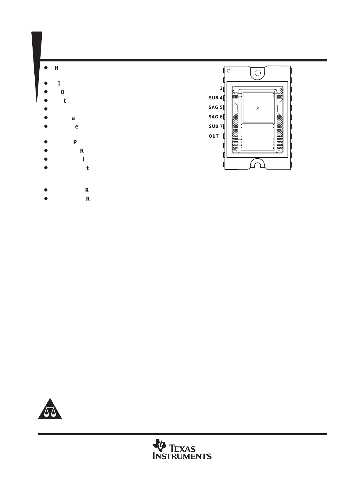
SUB 1
ODB 2
IAG 3
SUB 4
SAG 5
SAG 6
SUB 7
OUT 8
ADB 9
CDB 10
VGATE 11
22 SUB
21 TDB
20 IAG
19 SUB
18 SUB
17 SUB
16 NC
15 SRG
14 TRG
13 VSOURCE
12 RST
TI is a trademark of Texas Instruments Incorporated.
TC281
1036- × 1010-PIXEL CCD IMAGE SENSOR
SOCS058B – JUNE 1996 – REVISED MA Y 1999
2
POST OFFICE BOX 655303 • DALLAS, TEXAS 75265
description (continued)
The TC281 uses TI-proprietary advanced virtual-phase (A VP) technology , the advanced lateral-overflow-drain
structure, and the BCD detection node. These features provide the TI image sensing devices with a high blue
response, high near-IR sensitivity, low dark current, high photoresponse uniformity, and a single-phase
clocking. The TC281 is characterized for operation from -10_C to 45_C.
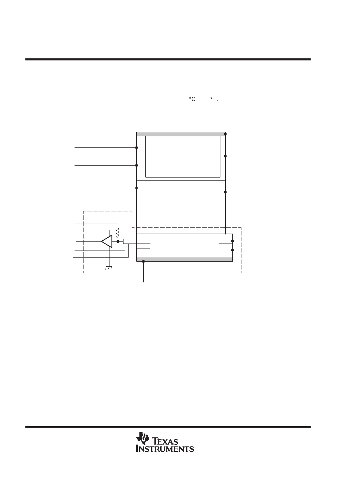
functional block diagram
Top Drain
Image Area
Storage Area
Serial Register
and Transfer Gate
Clearing Drain
21
20
5
15
14
TDB
10
11
12
88
9
13
Amplifier
6
3
2
ODB
IAG
SAG
V
SOURCE
ADB
OUT
RST
V
gate
CDB
IAG
SAG
SRG
TRG
ADVANCE INFORMATION
TC281
1036- × 1010-PIXEL CCD IMAGE SENSOR
SOCS058B – JUNE 1996 – REVISED MA Y 1999
3
POST OFFICE BOX 655303 • DALLAS, TEXAS 75265
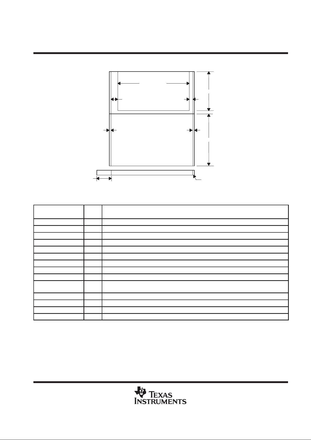
sensor topology diagram
1000 Pixels
28 Pixels 8 Pixels
1000 Lines
10 Lines
1010 Lines
1 Pixel1 Pixel
1 Dummy Pixel
10369
Dummy Pixels
Terminal Functions
TERMINAL
NAME NO.
I/O
DESCRIPTION
ADB 9 I Supply voltage for amplifier-drain bias
CDB 10 I Supply voltage for clearing-drain bias
IAG 3, 20 I Image area gate
NC 16 No connect
ODB 2 I Supply voltage overflow-drain antiblooming bias
OUT 8 O Output signal
RST 12 I Reset gate
SAG 5, 6 I Storage area gate
SRG 15 I Serial register gate 1
SUB
1, 4, 7, 17,
18, 19, 22
Substrate and clock return
TDB 21 NC Supply voltage for top-drain bias
TRG 14 I Transfer gate
VGATE 11 I Bias voltage for the gate of the BCD node
VSOURCE 13 I Bias voltage for the source of the BCD node
ADVANCE INFORMATION
TC281
1036- × 1010-PIXEL CCD IMAGE SENSOR
SOCS058B – JUNE 1996 – REVISED MA Y 1999
4
POST OFFICE BOX 655303 • DALLAS, TEXAS 75265
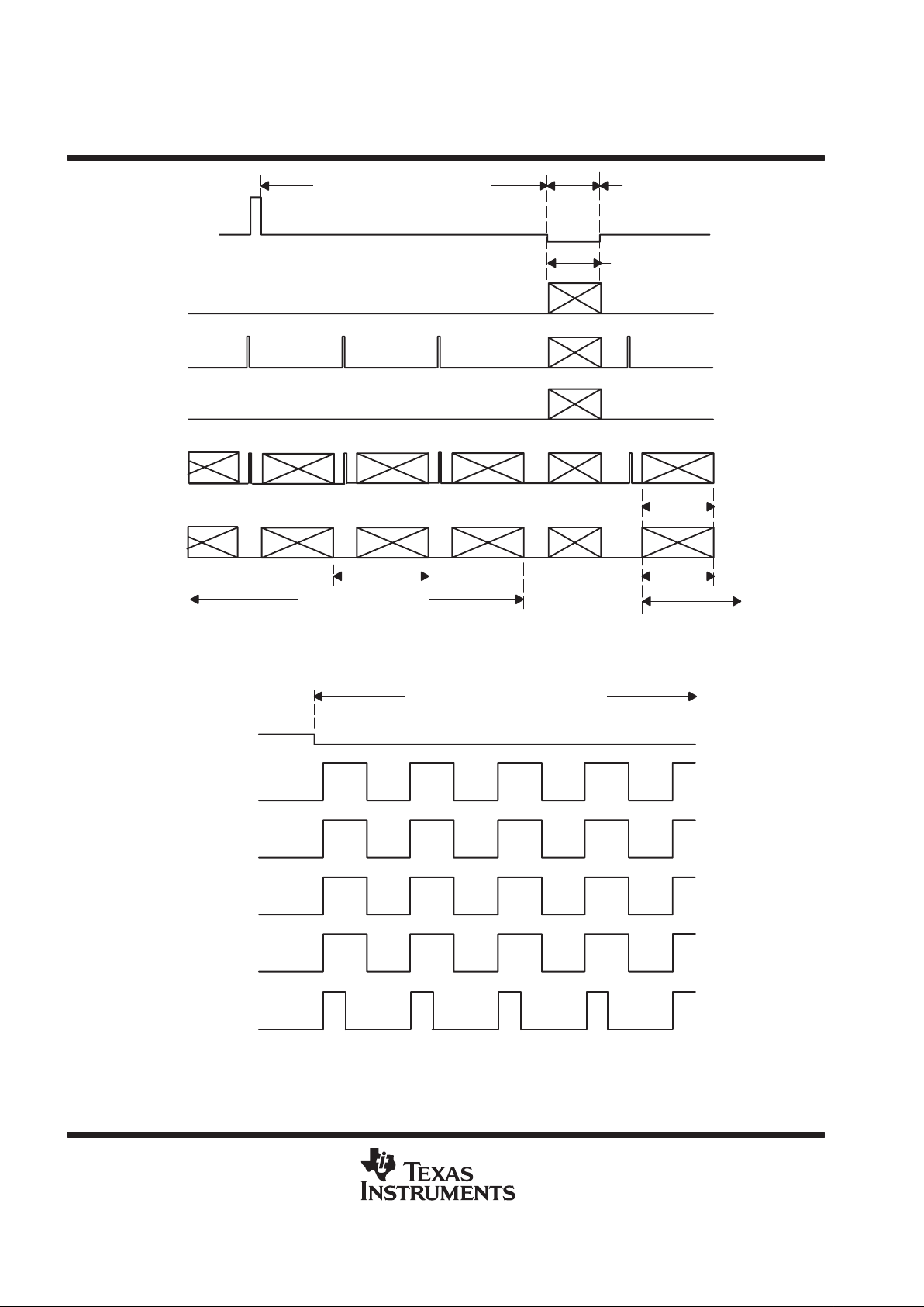
Integration Period Frame 2
Parallel Transfer
1010 Clocks
ODB
1046 Clocks
1010 Cycles
Readout Frame 2
Readout Frame 1
1046 Clocks
IAG
SAG
TRG
SRG
RST
Figure 1. Overview of Frame Timing with Variable Integration
Parallel Transfer 1010 Clocks
ODB
IAG
SAG
TRG
SRG
RST
Figure 2. Expanded Parallel Transfer Timing
ADVANCE INFORMATION

TC281
1036- × 1010-PIXEL CCD IMAGE SENSOR
SOCS058B – JUNE 1996 – REVISED MA Y 1999
5
POST OFFICE BOX 655303 • DALLAS, TEXAS 75265
1010 Cycles
Transfers One Line
From SA to SR
~1µs
Clears SRG During
Partial Line Readouts
Serial Line Readout
1046 Clocks
IAG
SAG
TRG
SRG
RST
Figure 3. Expanded Storage Area-to-Serial Register Transfer and Pixel Readout Timing
ODB
Storage Area Clear
9525 Clocks
IAG
SAG
TRG
SRG
RST
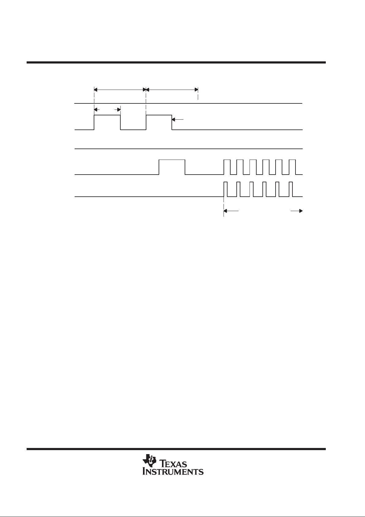
Figure 4. Special Modes of Operation: Storage Area Clear
ADVANCE INFORMATION
TC281
1036- × 1010-PIXEL CCD IMAGE SENSOR
SOCS058B – JUNE 1996 – REVISED MA Y 1999
6
POST OFFICE BOX 655303 • DALLAS, TEXAS 75265
IAG
~1µs
Transfer The
First Line From
SA to AR
Transfer The
Second Line
Adding to The First
Each Additional Pulse
Bins One Additional Line
Serial Line Readout
SAG
TRG
SRG
RST
Figure 5. Special Modes of Operation: Binning
detailed description
The TC281 image sensor consists of five basic functional blocks: 1) the image-sensing area, 2) the advanced
lateral overflow drain (ALOD), 3) the storage area, 4) the serial register, and 5) the bulk charge detection (BCD)
node with the buffer output amplifier.
image-sensing area
The image-sensing area contains 1036 x 1010 pixel elements. A metal light shield covers 28 pixels on the left
edge of the sensing area, 8 pixels on the right edge, and 10 rows at the bottom of the sensing area. The dark
pixel signal can be used as a black reference during the video signal processing. The dark references will
accumulate the dark current at the same rate as the active photosites, thus representing the true black level
signal. As light enters the active photosites in the image area, electron hole pairs are generated and the
electrons are collected in the potential wells of the pixels. The wells have a finite charge storage capacity
determined by the pixel design. When the generated number of electrons in the illuminated pixels exceeds this
limit, the electrons could spill over into neighboring pixels and cause blooming. To prevent this problem, each
horizontal pair of pixels in the image sensing area shares a lateral overflow drain structure which provides up
to a 1000-to-1 protection against such undesirable phenomenon.
advanced lateral overflow drain
The advanced lateral overflow drain structure is shared by two neighboring pixels and provides several unique
features thus available in the sensor. By varying the dc bias of the drain pin, it is possible to control the blooming
protection level and trade it for the well capacity.
Applying a 10-V pulse for a minimum duration of 1 us above the nominal dc bias level causes charge in the image
area to be completely cleared. This feature permits a precise control of the integration time on a frame-by-frame
basis. The single-pulse clear capability also reduces smear by eliminating accumulated charge from the pixels
before the start of the integration (single sided smear).
ADVANCE INFORMATION
 Loading...