

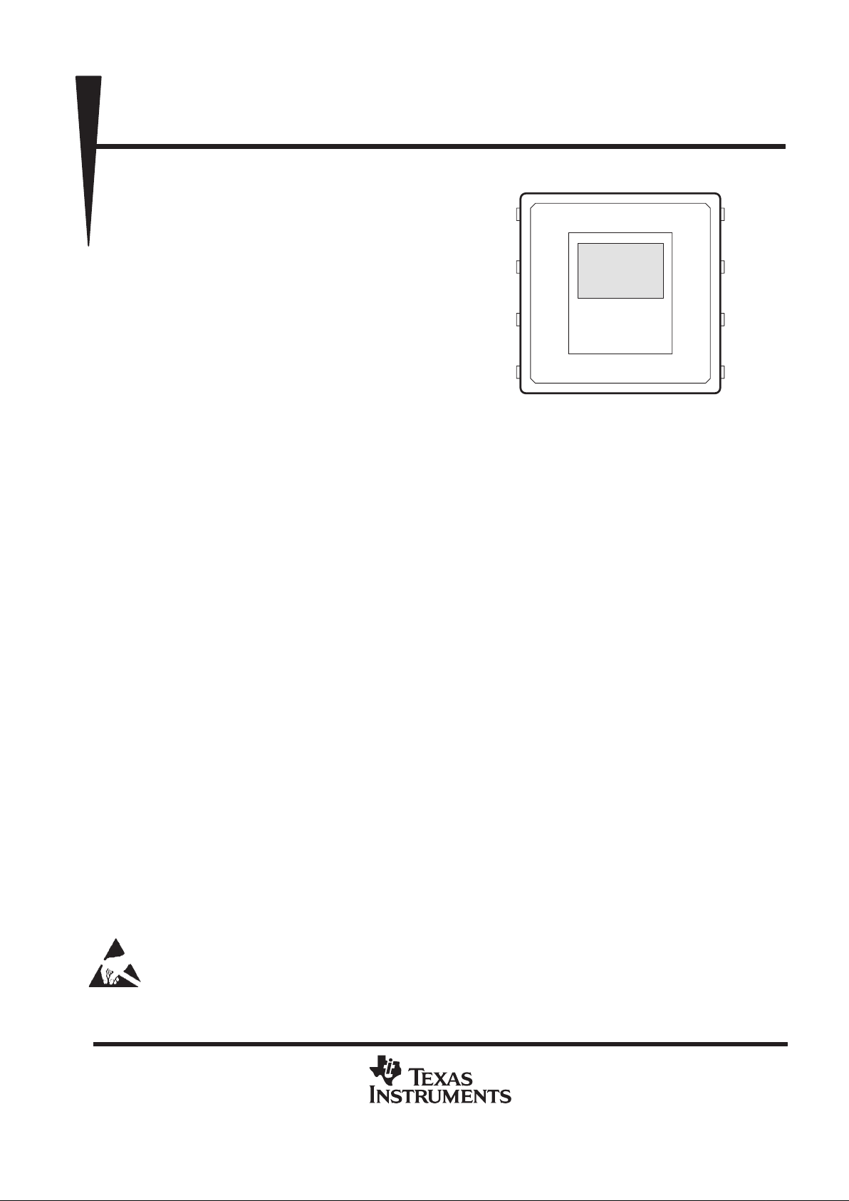
TC255P
336- × 244-PIXEL CCD IMAGE SENSOR
SOCS057 – JUNE 1996
Copyright 1996, Texas Instruments Incorporated
2-1
POST OFFICE BOX 655303 • DALLAS, TEXAS 75265
• Medium-Resolution, Solid-State Image
Sensor for Low-Cost B/W TV Applications
• 324(H) x 243(V) Active Elements in Image
Sensing Area
• 10-µm Square Pixels
• Fast Clear Capability
• Electronic Shutter Function From
1/60–1/50000 s
• Low Dark Current
• Electron-Hole Recombination Antiblooming
• Dynamic Range...66 dB Typical
• High Sensitivity
• High Blue Response
• 8-Pin Dual-In-Line Plastic Package
• 4-mm Image-Area Diagonal
• Solid-State Reliability With No Image
Burn-In, Residual Imaging, Image
Distortion, Image Lag, or Microphonics
• High Photoresponse Uniformity
description
The TC255P is a frame-transfer charge-coupled device (CCD) designed for use in B/W NTSC TV and specialpurpose applications where low cost and small size are desired.
The image-sensing area of the TC255P is configured in 243 lines with 336 elements in each line. Twelve
elements are provided in each line for dark reference. The blooming-protection feature of the sensor is based
on recombining excess charge with charge of opposite polarity in the substrate. This antiblooming is activated
by supplying clocking pulses to the antiblooming gate, which is an integral part of each image-sensing element.
The sensor can be operated in a noninterlace mode as a 324(H) by 243(V) sensor with low dark current. The
device can also be operated in an interlace mode, electronically displacing the image-sensing elements during
the charge integration in alternate fields, and effectively increasing the vertical resolution and minimizing
aliasing.
One important aspect of this image sensor is its high-speed image-transfer capability . This capability allows for
an electronic-shutter function comparable to interline-transfer and frame-interline-transfer sensors without the
loss of sensitivity and resolution inherent in those technologies.
The charge is converted to signal voltage with a 12-µV per electron conversion factor by a high-performance
charge-detection structure with built-in automatic reset and a voltage-reference generator. The signal is
buffered by a low-noise two-stage source-follower amplifier to provide high output-drive capability.
The TC255P uses TI-proprietary virtual-phase technology , which provides devices with high blue response, low
dark signal, high photoresponse uniformity, and single-phase clocking. The TC255P is characterized for
operation from –10°C to 45°C.
This MOS device contains limited built-in gate protection. During storage or handling, the device leads should be shorted together
or the device should be placed in conductive foam. In a circuit, unused inputs should always be connected to SUB. Under no
circumstances should pin voltages exceed absolute maximum ratings. Avoid shorting OUTn to ADB during operation to prevent
damage to the amplifier. The device can also be damaged if the output terminals are reverse-biased and an excessive current is
allowed to flow. Specific guidelines for handling devices of this type are contained in the publication
Guidelines for Handling
Electrostatic-Discharge-Sensitive (ESDS) Devices and Assemblies
available from Texas Instruments.
DUAL-IN-LINE PACKAGE
(TOP VIEW)
IAG2
ADB
SUB
OUT
ABG
IAG1
SAG
SRG
1
2
3
4
8
7
6
5
PRODUCTION DATA information is current as of publication date.
Products conform to specifications per the terms of Texas Instruments
standard warranty. Production processing does not necessarily include
testing of all parameters.
TC255P
336- × 244-PIXEL CCD IMAGE SENSOR
SOCS057 – JUNE 1996
2-2
POST OFFICE BOX 655303 • DALLAS, TEXAS 75265
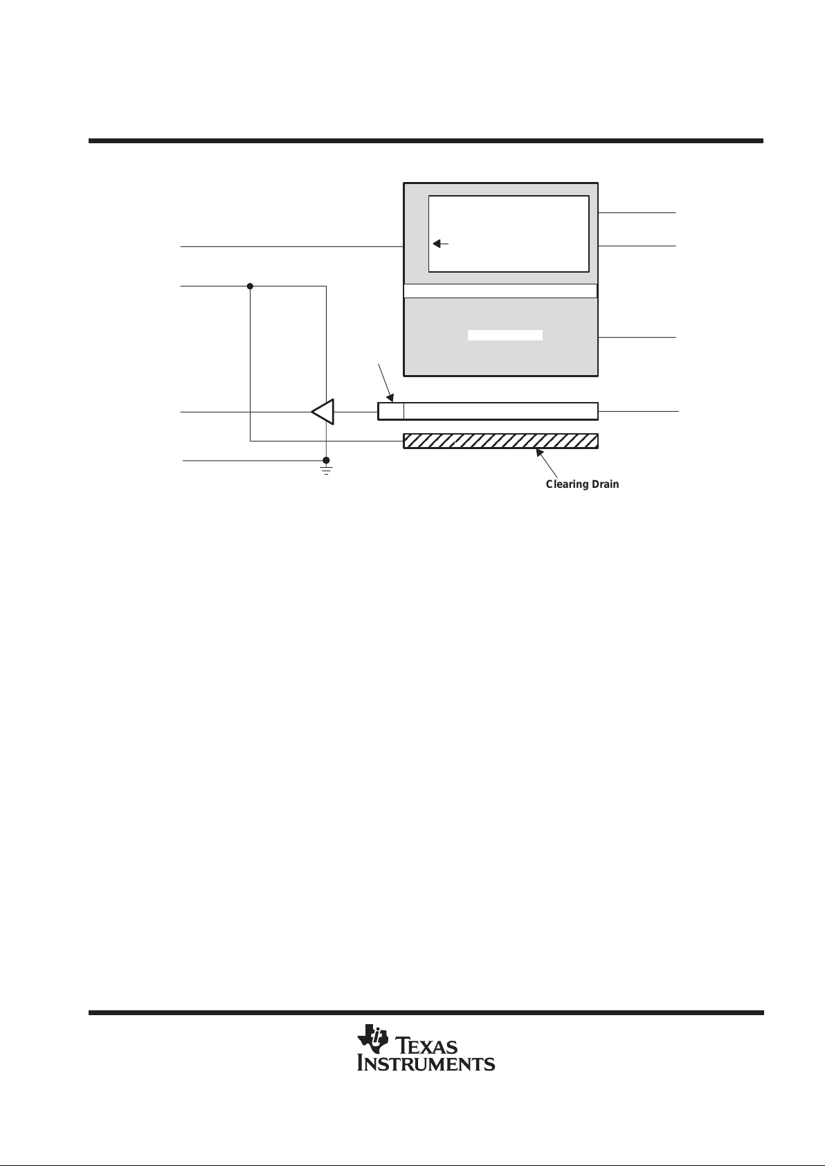
functional block diagram
Amplifier
OUT
ADB
IAG2
1
4
SAG
6
IAG1
ABG
7
8
Storage Area
Blooming Protection
Image Area With
Dark-Reference Elements
2
SUB
2 Dummy
Elements
3
Serial Register
SRG
5
Clear Line
Clearing Drain
TC255P
336- × 244-PIXEL CCD IMAGE SENSOR
SOCS057 – JUNE 1996
2-3
POST OFFICE BOX 655303 • DALLAS, TEXAS 75265
sensor topology diagram
Effective-Imaging Area
324 Active Pixels
12
243 Lines
1 Dark Line
1 Clear Line
244 Lines
336 Pixels
212 1324Dummy Pixels
Optical
Black
(OPB)
Dummy Pixel
Buffer Column
Active Pixels
Storage Area
Terminal Functions
TERMINAL
NAME NO.
I/O
DESCRIPTION
ABG 8 I Antiblooming gate
ADB 2 I Supply voltage for amplifier-drain bias
SUB 3 Substrate
IAG1 7 I Image-area gate 1
IAG2 1 I Image-area gate 2
OUT 4 O Output
SAG 6 I Storage-area gate
SRG 5 I Serial-register gate
TC255P
336- × 244-PIXEL CCD IMAGE SENSOR
SOCS057 – JUNE 1996
2-4
POST OFFICE BOX 655303 • DALLAS, TEXAS 75265
detailed description
The TC255P consists of five basic functional blocks: 1) the image-sensing area, 2) the image-clear line, 3) the
image-storage area, 4) the serial register, and 5) the charge-detection node and output amplifier.
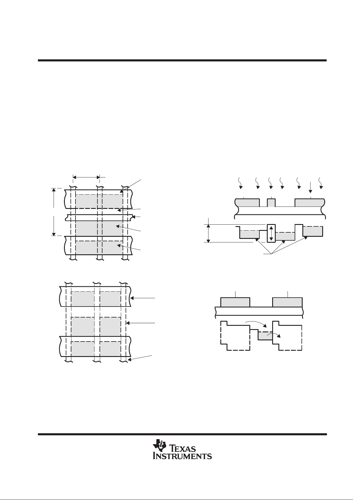
image-sensing area
Cross sections with potential-well diagrams and top views of image-sensing and storage-area elements are
shown in Figure 1 and Figure 2. As light enters the silicon in the image-sensing area, free electrons are
generated and collected in the potential wells of the sensing elements. During this time, the antiblooming gate
is activated by the application of a burst of pulses every horizontal-blanking interval. This prevents blooming
caused by the spilling of charge from overexposed elements into neighboring elements. To generate the dark
reference that is necessary in subsequent video-processing circuits for restoration of the video-black level, there
are 12 columns of elements on the left edge of the image-sensing area shielded from light. There is also one
column of elements on the right side of the image-sensing area and one line between the image-sensing area
and the image-clear line.
ABG
IAG
10 µm
Clocked Barrier
Virtual Barrier
Antiblooming Gate
Virtual Well
Clocked Well
Light
Antiblooming
Clocking Levels
Accumulated Charge
10 µm
Figure 1. Charge-Accumulation Process
SAG
Channel Stops
Virtual Phase
Clocked Phase
Figure 2. Charge-Transfer Process
image-clear line
During start-up or electronic-shutter operations, it is necessary to clear the image area of charge without
transferring it to the storage area. In such situations, the two image-area gates are clocked 244 times without
clocking the storage-area gate. The charge in the image area is then cleared through the image-clear line.
TC255P
336- × 244-PIXEL CCD IMAGE SENSOR
SOCS057 – JUNE 1996
2-5
POST OFFICE BOX 655303 • DALLAS, TEXAS 75265
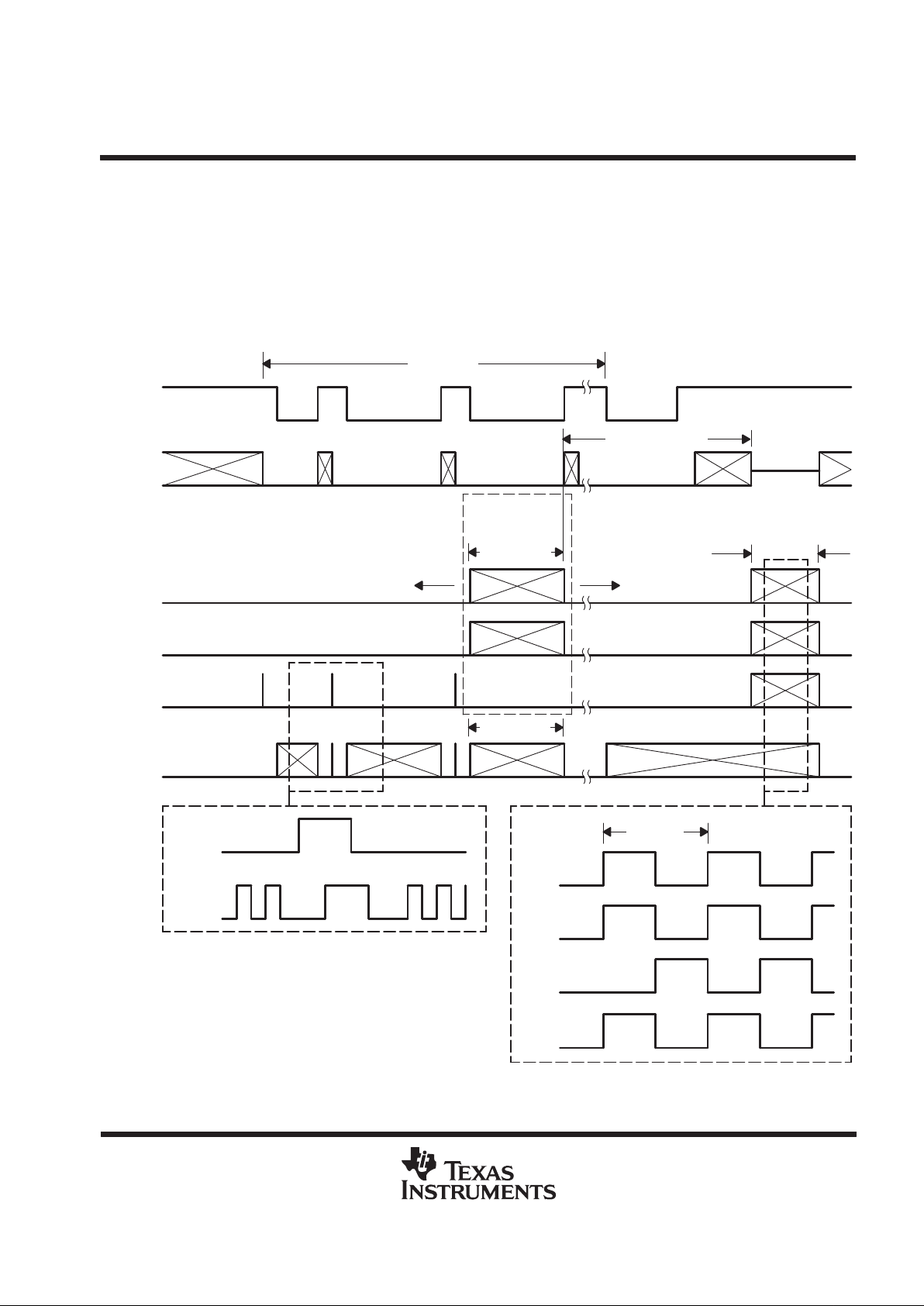
image-storage area
After exposure, the image-area charge packets are transferred through the image-clear line to the storage area.
The stored charge is then transferred line by line into the serial register for readout. Figure 3 illustrates the timing
to (1) transfer the image to the storage area and (2) to transfer each line from the storage area to the serial
register.
serial register
After each line is clocked into the serial register, it is read out pixel by pixel. Figure 3 illustrates the serial-register
clock sequence.
SAG
SRG
IAG1
IAG2
SAG
Expanded Section of Parallel Transfer
1) 2) 3)
1) End of serial readout of line
2) Transfer of new line to serial register
3) Beginning of readout of new line
244 Clocks
244 Cycles
Composite
Blank
ABG
IAG1
IAG2
SAG
SRG
339 Cycles
SRG
t = 80 ns
244 Clocks
Electronic
Shutter
Operation
Integration Time
Figure 3. Timing Diagram
TC255P
336- × 244-PIXEL CCD IMAGE SENSOR
SOCS057 – JUNE 1996
2-6
POST OFFICE BOX 655303 • DALLAS, TEXAS 75265
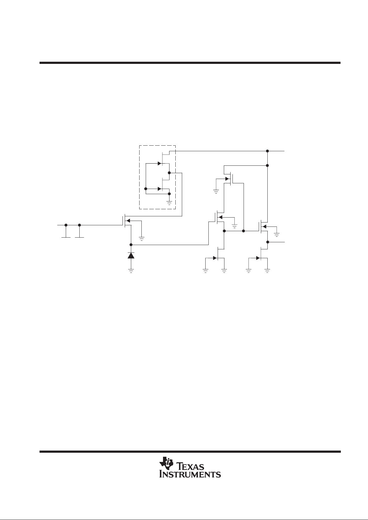
charge-detection node and output amplifier
The buffer amplifier converts charge into a video signal. Figure 4 shows the circuit diagram of the
charge-detection node and output amplifier. As charge is transferred into the detection node, the potential of
this node changes in proportion to the amount of signal received. This change is sensed by an MOS transistor
and, after proper buffering, the signal is supplied to the output terminal of the image sensor . After the potential
change is sensed, the node is reset to a reference voltage supplied by an on-chip reference generator. The reset
is accomplished by a reset gate that is connected internally to the serial register. The detection node and buf fer
amplifier are located a short distance from the edge of the storage area; therefore, two dummy cells are used
to span this distance.
Reference
Generator
Q0
Q1
Q2
Q3
Q5
Q6
V
O
Q4
QR
SRG
Detection
Node
ADB
Figure 4. Buffer Amplifier and Charge-Detection Node

TC255P
336- × 244-PIXEL CCD IMAGE SENSOR
SOCS057 – JUNE 1996
2-7
POST OFFICE BOX 655303 • DALLAS, TEXAS 75265
spurious-nonuniformity specification
The spurious-nonuniformity specification of the TC255P is based on several sensor characteristics:
• Amplitude of the nonuniform pixel
• Polarity of the nonuniform pixel
– Black
– White
• Column amplitude
The CCD sensor is characterized in both an illuminated condition and a dark condition. In the dark condition,
the nonuniformity is specified in terms of absolute amplitude as shown in Figure 5. In the illuminated condition,
the nonuniformity is specified as a percentage of the total illumination as shown in Figure 6.
The specification for the TC255P is as follows:
WHITE SPOT
(DARK)
WHITE SPOT
(ILLUMINATED)
COLUMN
(DARK)
COLUMN
(ILLUMINATED)
BLACK SPOT
(ILLUMINATED)
WHITE/BLACK
†
PAIR
x < 15 mV x < 15% x < 0.5 mV x < 1 mV x < 15% x < 9mV
†
A white/black pair nonuniformity will be no more than 2 pixels even for integration times of 1/60 second.
The conditions under which this specification is defined are as follows:
• The integration time is 1/60 second except for illuminated white spots, illuminated black spots and
white/black pair nonuniformities; in these three cases, the integration time is 1/240 second.
• The temperature is 45°C.
• The CCD video-output signal is 60 mV ± 10 mV.
mV
Amplitude
t
Illumination
% of Total
t
%
Figure 5. Pixel Nonuniformity, Figure 6. Pixel Nonuniformity,
Dark Condition Illuminated Condition

TC255P
336- × 244-PIXEL CCD IMAGE SENSOR
SOCS057 – JUNE 1996
2-8
POST OFFICE BOX 655303 • DALLAS, TEXAS 75265
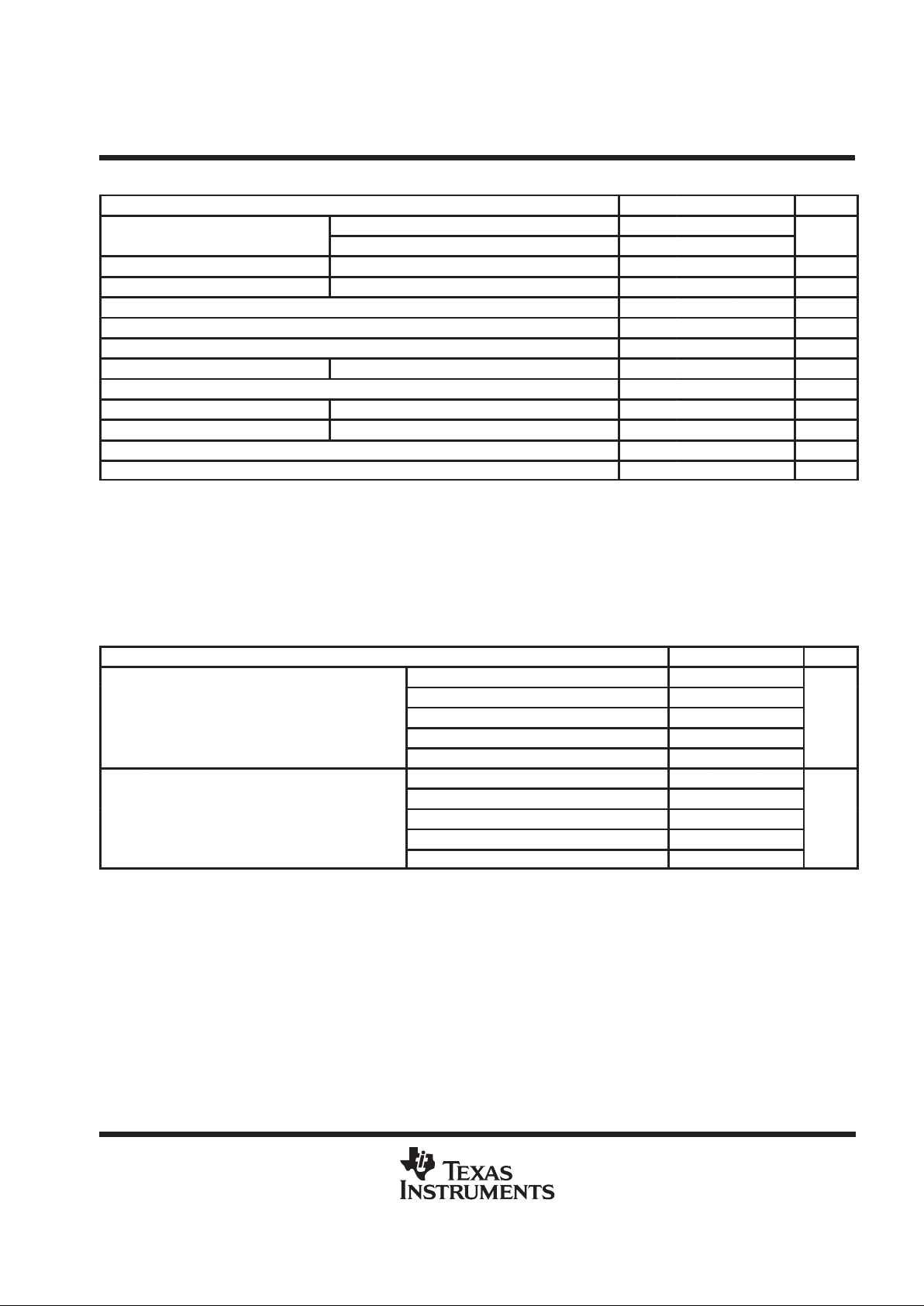
absolute maximum ratings over operating free-air temperature (unless otherwise noted)
†
Supply voltage range, V
CC
: ADB (see Note 1) 0 V to 15 V. . . . . . . . . . . . . . . . . . . . . . . . . . . . . . . . . . . . . . . . . .
Input voltage range, V
I
: ABG, IAG1, IAG2, SAG, SRG –15 V to 15 V. . . . . . . . . . . . . . . . . . . . . . . . . . . . . . . . .
Operating free-air temperature range, T
A
–10°C to 45°C. . . . . . . . . . . . . . . . . . . . . . . . . . . . . . . . . . . . . . . . . . . .
Storage temperature range, T
STG
–30°C to 85°C. . . . . . . . . . . . . . . . . . . . . . . . . . . . . . . . . . . . . . . . . . . . . . . . . . .
†
Stresses beyond those listed under “absolute maximum ratings” may cause permanent damage to the device. These are stress ratings only, and
functional operation of the device at these or any other conditions beyond those indicated under “recommended operating conditions” is not
implied. Exposure to absolute-maximum-rated conditions for extended periods may affect device reliability.
NOTE 1: All voltages are with respect to the substrate terminal.
recommended operating conditions
MIN NOM MAX UNIT
Supply voltage, V
CC
ADB 11 12 13 V
Substrate bias voltage 0 V
High level 1.5 2 2.5
IAG1, IAG2
Low level –10.5 –10 –9.5
High level 1.5 2 2.5
SAG
Low level –10.5 –10 –9.5
Input voltage, V
I
High level 1.5 2 2.5
V
SRG
Low level –10.5 –10 –9.5
High level 3.5 4 4.5
ABG
Intermediate level
‡
–2.5
Low level –8 –7 –6
ABG 6.25 12.5
IAG1, IAG2
25
Clock frequenc
y,
f
clock
SAG
12.5
MH
z
SRG
6.25 12.5
Load capacitive OUT 6 pF
Plastic package thermal conductivity 0.008 J/cm•s•°C
Operating free-air temperature, T
A
–10 45 °C
‡
Adjustment is required for optimum performance.

TC255P
336- × 244-PIXEL CCD IMAGE SENSOR
SOCS057 – JUNE 1996
2-9
POST OFFICE BOX 655303 • DALLAS, TEXAS 75265
electrical characteristics over recommended operating ranges of supply voltage and operating
free-air temperature (unless otherwise noted)
PARAMETER MIN TYP
†
MAX UNIT
Dynamic range (see Note 2) Antiblooming disabled (see Note 3) 66 dB
Charge-conversion factor 11 12 13 µV/e
Charge-transfer efficiency (see Note 4) 0.9995 0.99999
Signal-response delay time, τ (see Note 5) 20 ns
Gamma (see Note 6) 0.97 0.98 0.99
Output resistance 350 Ω
Noise-equivalent signal without correlated double sampling 62 electrons
Noise-equivalent signal with correlated double sampling (see Note 7) 31 electrons
ADB (see Note 8) 13 15 18
Rejection ratio
SRG (see Note 9) 50
dB
ABG (see Note 10) 40
Supply current 5 10 mA
IAG1, IAG2 1000
p
p
SRG 22
p
Input capacitance, C
i
ABG 850
pF
SAG 2000
†
All typical values are at TA = 25°C.
NOTES: 2. Dynamic range is –20 times the logarithm of the mean-noise signal divided by saturation-output signal.
3. For this test, the antiblooming gate must be biased at the intermediate level.
4. Charge-transfer efficiency is one minus the charge loss per transfer in the output register. The test is performed in the dark using
an electrical-input signal.
5. Signal-response delay time is the time between the falling edge of the SRG pulse and the output-signal valid state.
6. Gamma (γ) is the value of the exponent is the equation below for two points on the linear portion of the transfer-function curve (this
value represents points near saturation).
ǒ
Exposure (2)
Exposure (1)
Ǔ
g
+
ǒ
Output signal (2)
Output signal (1)
Ǔ
7. A three-level serial-gate clock is necessary to implement correlated double sampling.
8. ADB rejection ratio is –20 times the logarithm of the ac amplitude at the output divided by the ac amplitude at ADB (see Figure 11
for measured ADB rejection ratio as a function of frequency).
9. SRG rejection ratio is –20 times the logarithm of the ac amplitude at the output divided by the ac amplitude at SRG.
10. ABG rejection ratio is –20 times the logarithm of the ac amplitude at the output divided by the ac amplitude at ABG.
TC255P
336- × 244-PIXEL CCD IMAGE SENSOR
SOCS057 – JUNE 1996
2-10
POST OFFICE BOX 655303 • DALLAS, TEXAS 75265
optical characteristics, TA = 40°C (unless otherwise noted)
PARAMETER MIN TYP MAX UNIT
No IR filter 350
Sensitivit
y
With IR filter 45
mV/l
x
Saturation signal, V
sat
(see Note 11) Antiblooming disabled, Interlace off 600 750 mV
Maximum usable signal, V
use
Antiblooming enabled 200 250 mV
Blooming-overload ratio (see Note 12) 100 200
Image-area well capacity 50000 62500 electrons
Smear (see Notes 13 and 14) 0.00012
Dark current Interlace disabled, TA = 21°C 0.20 nA/cm
2
Dark signal 200 µV
Pixel uniformity Output signal = 60 mV ± 10 mV 15 mV
Column uniformity Output signal = 60 mV ± 10 mV 0.5 mV
Shading 15 %
Electronic-shutter capability 1/15000 1/60 s
NOTES: 11. Saturation is the condition in which further increase in exposure does not lead to further increase in output signal.
12. Blooming is the condition in which charge is induced in an element by light incident on another element. Blooming-overload ratio
is the ratio of blooming exposure to saturation exposure.
13. Smear is a measure of the error introduced by transferring charge through an illuminated pixel in shutterless operation. It is equivalent
to the ratio of the single-pixel transfer time to the exposure time using an illuminated section that is 1/10 of the image-area vertical
height with recommended clock frequencies.
14. The exposure time is 16.67 ms, the fast-dump clocking rate during vertical transfer is 12.5 MHz, and the illuminated section is 1/10
of the height of the image section.
timing requirements
MIN NOM MAX UNIT
ABG 10 40
IAG1, IAG2 (fast clear) 10 10
t
r
Rise time
IAG1, IAG2 (image transfer)
10 20
ns
SAG 10 20
SRG 10 40
ABG 10 40
IAG1, IAG2 (fast clear) 10 10
t
f
Fall time
IAG1, IAG2 (image transfer)
10 20
ns
SAG 10 20
SRG 10 40

TC255P
336- × 244-PIXEL CCD IMAGE SENSOR
SOCS057 – JUNE 1996
2-11
POST OFFICE BOX 655303 • DALLAS, TEXAS 75265
PARAMETER MEASUREMENT INFORMATION
DR (dynamic range)+20 log
ǒ
V
sat
Ǔ
V
n
d
B
Vn = noise-floor voltage
V
sat (min)
= minimum saturation voltage
V
use (max)
= maximum usable voltage
V
use (typ)
= typical user voltage (camera white clip)
NOTES: A. V
use (typ)
is defined as the voltage determined to equal the camera white clip. This voltage must be less than V
use
(max)
.
B. A system trade-off is necessary to determine the system light sensitivity versus the signal/noise ratio. By lowering
the V
use(typ)
,
the light sensitivity of the camera is increased; however, this sacrifices the signal/noise ratio of the camera.
SNR (signal-to-noise-rate)+20 log
ǒ
V
use
Ǔ
V
n
d
B
(light input)
Lux
Enabled
With Antiblooming
Blooming Point
Well Capacity
Dependent on
Disabled
With Antiblooming
Blooming Point
Gate High Level
Upon Antiblooming
Level Dependent
SNR
V
n
V
sat (min)
V
use (typ)
V
use (max)
V
O
DR
Figure 7. Typical V
sat,
V
use
Relationship

TC255P
336- × 244-PIXEL CCD IMAGE SENSOR
SOCS057 – JUNE 1996
2-12
POST OFFICE BOX 655303 • DALLAS, TEXAS 75265
PARAMETER MEASUREMENT INFORMATION
– 8.5 V
1.5 V to 2.5 V
– 8.5 V to –10 V
0%
15 ns10 ns
t
CCD Delay
SRG
OUT
90%
100%
Sample
and
Hold
Figure 8. SRG and CCD Output Waveforms

TC255P
336- × 244-PIXEL CCD IMAGE SENSOR
SOCS057 – JUNE 1996
2-13
POST OFFICE BOX 655303 • DALLAS, TEXAS 75265
TYPICAL CHARACTERISTICS
300 400 500 600 700 800 900 1000
0.001
0.01
0.1
1
CCD SPECTRAL RESPONSIVITY
Responsivity – A/W
Incident Wavelength – nm
Figure 9
300 400 500 600 700 800 900 1000
0.001
0.01
0.1
1
CCD QUANTUM EFFICIENCY
Quantum Efficiency
Incident Wavelength – nm
Figure 10

TC255P
336- × 244-PIXEL CCD IMAGE SENSOR
SOCS057 – JUNE 1996
2-14
POST OFFICE BOX 655303 • DALLAS, TEXAS 75265
TYPICAL CHARACTERISTICS
0 5 10 25
0
ADB Rejection Ratio – dB
f – Frequency – MHz
2
4
6
8
10
12
14
16
18
20
15 20
Figure 11. Measured ADB Rejection Ratio as a Function of Frequency
0 5 10 25
0
Noise-Power Spectral Density –nV/rt Hz
f – Frequency – MHz
50
100
150
200
250
300
15 20
Figure 12. Noise-Power Spectral Density

TC255P
336- × 244-PIXEL CCD IMAGE SENSOR
SOCS057 – JUNE 1996
2-15
POST OFFICE BOX 655303 • DALLAS, TEXAS 75265
APPLICATION INFORMATION
IAG1
SAG
SRG
IAG2
ADB
SUB
OUT
TC255P
ABG
8
7
6
5
1
2
3
4
VIA, VM, V
S
12 V
DC VOLTAGES
TMC57750
4443424140393837363534
54
55
56
57
58
59
60
61
62
63
64
27
26
25
24
23
22
21
20
19
18
17
56789101112131415
28
29
30
31
45 46 47 48
4321
53
52
51
50
WSEL2
ED
DSSEL
PHSEL1
FI
TEST1
S/H
SHTCOM
EU
TEST4
CBLK
CSYNC
GND
CPOB1
CPOB2
SSEL1
V
CC
SSEL2
SSEL3
VR
HR
WSEL1
CC
MINSEL
EFSEL3
EFSEL2
EFSEL1
MON4
MON3
MON2
MON1
GND
TEST3
TEST2
FSSEL
ABGSEL
ABG
ABM
V
CC
IAG1
IAG2
SAG
GND
SRG
SRM
DLSEL
PHSEL2
CDS
GND
MCLK/4
MCLK/2
XSEL
XOUT
XIN
CLKIN
SCAN
PUCHDVD
32
V
ACT
16
49
SRGSEL
33
SHTMON
V
WINDOW
V
CC
WIN
V
CC
CPOB1
CSYNC
CBLK
EU
ED
V
CC
S/H
CDS
V
CC
OUT
5 V
GND
V
CC
25 MHz
V
CC
V
CC
GND
EN
V
AB
1
2
3
4
5
6
7
8
9
10
11
12
ABIN
ABMIN
IA1IN
IA2IN
SAIN
SRIN
SRMIN
GND
24
23
22
21
20
19
18
17
16
15
14
13
ABOUT
V
ABL
GND
V
ABM
IA1OUT
V
IA
IA2OUT
GND
SAOUT
V
S
SROUT
V
SM
V
AB
V
CC
TMC57253
V
ABM
ADB
SUB
V
IA
V
S
V
SM
Buffer
and
Preamp
SN761210
18171615141312
6
5
4
3
2
1
7
8
9
10
19 20 21 22
DELA YIN
AGCOUT
DATAIN
S/HFB
SHP
SHD1
SHD2
GND
AGCFIL
AGCLVL
AGCMAX
IRIS
WINDOW
HOBP
GND
AGCFB
AMPTUNE
GAINSEL
AMPOUT
YIN
11
AMPIN
CHD
28
29
30
31
32
33
27
26
25
24
23
APGAIN
V
CC
VIDEO
GND
CSYNC
CLAMP
CHARAIN
V
CC
YHIN
APOUT
APFIL
38394041424344
37 36 35 34
CBLK
V
CENTER
WIDTH
IRISFIL
LOB
HIB
VREF
SYNCLVL
SULVL
HICPLVL
CC
CBLK
V
CTRLVL
WIDLVL
ED
EU
SYNCLVL
SULVL
HICPLVL
CC
4.7 µF
0.1 µF
0.1 µF
S/H
CDS
4.7 µF
Low-Pass
FIlter
0.1 µF
WIN
CPOB1
0.1 µF
AMPTUNE
V
CC
75Ω
CSYNC
CPOB1
To Monitor
V
CC
0.1 µF
V
CC
5 V
ADB 22 V
SUB 10 V
V
ABM
7.5 V
HICPLVL 1.9 V
SULVL 1.2 V
SYNCLVL 1.2 V
CTRLVL 1.0 V
WIDLVL 4.0 V
AMPTUNE 1.0 V
100 µF
V
CC
V
AB
V
ABL
14 V
3 V
NOTES: A. Decoupling capacitors are not shown.
B. TI recommends designing AC coupled systems.
(see
NoteB)
V
ABL
Figure 13. Typical Application Circuit Diagram

TC255P
336- × 244-PIXEL CCD IMAGE SENSOR
SOCS057 – JUNE 1996
2-16
POST OFFICE BOX 655303 • DALLAS, TEXAS 75265
APPLICATION INFORMATION
SUPPORT CIRCUITS
DEVICE PACKAGE APPLICATION FUNCTION
TMC57750PM 64 pin flatpack Timing generator EIA-170 timing and CCD control signals
TMC57253DSB 24 pin small outline Driver Driver for ABG, IAG1, IAG2, SAG, and SRG
SN761210FR 44 pin flatpack Video processor
SYNC, BLANK, AGC, IRIS, CLAMP, S/H, CDS, and
WINDOW
Figure 13. Typical Application Circuit Diagram (Continued)

TC255P
336- × 244-PIXEL CCD IMAGE SENSOR
SOCS057 – JUNE 1996
2-17
POST OFFICE BOX 655303 • DALLAS, TEXAS 75265
MECHANICAL DATA
The package for the TC255P consists of a plastic base, a glass window, and an 8-lead frame. The glass window is
sealed to the package by an epoxy adhesive. The package leads are configured in a dual in-line organization and
fit into mounting holes with 2,54 mm (0.1 in) center-to-center spacings.
Î
Î
Î
Î
Package Center
10,05
9,95
9,00
8,90
10,05
9,95
9,00
8,90
5,19
4,93
4,20
3,93
0,64
1,273,50
2,54
0,46
0,30
0,50
0,80
0,70
2,67
2,53
0,27
0,23
10,16
Chip Surface
1,10
1,20
1,50
1,40
Optical
Center
6/96
ALL LINEAR DIMENSIONS ARE IN MILLIMETERS AND PARENTHETICALLY IN INCHES
TC255P (8 pin)

IMPORTANT NOTICE
T exas Instruments and its subsidiaries (TI) reserve the right to make changes to their products or to discontinue
any product or service without notice, and advise customers to obtain the latest version of relevant information
to verify, before placing orders, that information being relied on is current and complete. All products are sold
subject to the terms and conditions of sale supplied at the time of order acknowledgement, including those
pertaining to warranty, patent infringement, and limitation of liability.
TI warrants performance of its semiconductor products to the specifications applicable at the time of sale in
accordance with TI’s standard warranty. Testing and other quality control techniques are utilized to the extent
TI deems necessary to support this warranty. Specific testing of all parameters of each device is not necessarily
performed, except those mandated by government requirements.
CERT AIN APPLICATIONS USING SEMICONDUCTOR PRODUCTS MAY INVOLVE POTENTIAL RISKS OF
DEATH, PERSONAL INJURY, OR SEVERE PROPERTY OR ENVIRONMENTAL DAMAGE (“CRITICAL
APPLICATIONS”). TI SEMICONDUCTOR PRODUCTS ARE NOT DESIGNED, AUTHORIZED, OR
WARRANTED TO BE SUITABLE FOR USE IN LIFE-SUPPORT DEVICES OR SYSTEMS OR OTHER
CRITICAL APPLICATIONS. INCLUSION OF TI PRODUCTS IN SUCH APPLICA TIONS IS UNDERST OOD TO
BE FULLY AT THE CUSTOMER’S RISK.
In order to minimize risks associated with the customer’s applications, adequate design and operating
safeguards must be provided by the customer to minimize inherent or procedural hazards.
TI assumes no liability for applications assistance or customer product design. TI does not warrant or represent
that any license, either express or implied, is granted under any patent right, copyright, mask work right, or other
intellectual property right of TI covering or relating to any combination, machine, or process in which such
semiconductor products or services might be or are used. TI’s publication of information regarding any third
party’s products or services does not constitute TI’s approval, warranty or endorsement thereof.
Copyright 1998, Texas Instruments Incorporated
 Loading...