

Texas Instruments SN74ACT3631-15PCB, SN74ACT3631-15PQ, SN74ACT3631-20PCB, SN74ACT3631-20PQ, SN74ACT3631-30PCB Datasheet
...
SN74ACT3631
CLOCKED FIRST-IN, FIRST-OUT MEMORY
SCAS246G – AUGUST 1993 – REVISED APRIL 1998
D
Free-Running CLKA and CLKB Can Be
Asynchronous or Coincident
D
Clocked FIFO Buffering Data From Port A
to Port B
D
Synchronous Read-Retransmit Capability
D
Mailbox Register in Each Direction
D
Programmable Almost-Full and
Almost-Empty Flags
D
Microprocessor Interface Control Logic
D
Input-Ready and Almost-Full Flags
Synchronized by CLKA
description
The SN74ACT3631 is a high-speed, low-power, CMOS clocked FIFO memory. It supports clock frequencies
up to 67 MHz and has read access times as fast as 1 1 ns. The 512 × 36 dual-port SRAM FIFO buffers data from
port A to port B. The FIFO memory has retransmit capability , which allows previously read data to be accessed
again. The FIFO has flags to indicate empty and full conditions and two programmable flags (almost full and
almost empty) to indicate when a selected number of words is stored in memory . Communication between each
port can take place with two 36-bit mailbox registers. Each mailbox register has a flag to signal when new mail
has been stored. Two or more devices can be used in parallel to create wider datapaths. Expansion also is
possible in word depth.
D
Output-Ready and Almost-Empty Flags
Synchronized by CLKB
D
Low-Power 0.8-µm Advanced CMOS
Technology
D
Supports Clock Frequencies up to 67 MHz
D
Fast Access Times of 11 ns
D
Pin-to-Pin Compatible With the
SN74ACT3641 and SN74ACT3651
D
Package Options Include 120-Pin Thin
Quad Flat (PCB) and 132-Pin Plastic Quad
Flat (PQ) Packages
512 × 36
The SN74ACT3631 is a clocked FIFO, which means each port employs a synchronous interface. All data
transfers through a port are gated to the low-to-high transition of a continuous (free-running) port clock by enable
signals. The continuous clocks for each port are independent of one another and can be asynchronous or
coincident. The enables for each port are arranged to provide a simple interface between microprocessors
and/or buses with synchronous control.
The input-ready (IR) flag and almost-full (AF
output-ready (OR) flag and almost-empty (AE
values for the AF and AE flags of the FIFO can be programmed from port A or through a serial input.
The SN74ACT3631 is characterized for operation from 0°C to 70°C.
For more information on this device family, see the following application reports:
D
FIFO Patented Synchronous Retransmit: Programmable DSP-Interface Application for FIR Filtering
(literature number SCAA007)
D
FIFO Mailbox-Bypass Registers: Using Bypass Registers to Initialize DMA Control
SCAA007)
D
Metastability Performance of Clocked FIFOs (literature number SCZA004).
) flag of the FIFO are two-stage synchronized to CLKA. The
) flag of the FIFO are two-stage synchronized to CLKB. Offset
(literature number
Please be aware that an important notice concerning availability, standard warranty, and use in critical applications of
Texas Instruments semiconductor products and disclaimers thereto appears at the end of this data sheet.
PRODUCTION DATA information is current as of publication date.
Products conform to specifications per the terms of Texas Instruments
standard warranty. Production processing does not necessarily include
testing of all parameters.
POST OFFICE BOX 655303 • DALLAS, TEXAS 75265
Copyright 1998, Texas Instruments Incorporated
1
SN74ACT3631
512 × 36
CLOCKED FIRST-IN, FIRST-OUT MEMORY
SCAS246G – AUGUST 1993 – REVISED APRIL 1998
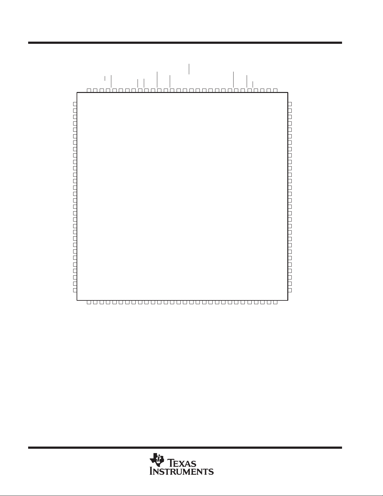
PCB PACKAGE
(TOP VIEW)
A35
A34
A33
A32
V
CC
A31
A30
GND
A29
A28
A27
A26
A25
A24
A23
GND
A22
V
CC
A21
A20
A19
A18
GND
A17
A16
A15
A14
A13
V
CC
A12
1
2
3
4
5
6
7
8
9
10
11
12
13
14
15
16
17
18
19
20
21
22
23
24
25
26
27
28
29
30
GND
CLKA
119
120
32
31
ENA
W/RA
117
118
33
CSAIROR
116
35
34
115
36
114
37
V
113
38
CC
CC
MBF2
V
110
41
MBAAFGND
108
109
43
42
AE
111
112
40
39
RST
107
44
FS0/SD
105
106
46
45
FS1/SEN
104
47
RTM
103
48
V
RFM
101
102
49
50
CC
NC
100
51
GND
MBB
98
99
53
52
MBF1
CSB
GND
96
97
95
54
5556575859
W/RB
94
ENB
CLKB
92
93
CC
V
91
60
90
89
88
87
86
85
84
83
82
81
80
79
78
77
76
75
74
73
72
71
70
69
68
67
66
65
64
63
62
61
B35
B34
B33
B32
GND
B31
B30
B29
B28
B27
B26
V
CC
B25
B24
GND
B23
B22
B21
B20
B19
B18
GND
B17
B16
V
CC
B15
B14
B13
B12
GND
A9
A8
A7
A1 1
A10
GND
NC – No internal connection
2
A6
A4
A5
A3
GND
POST OFFICE BOX 655303 • DALLAS, TEXAS 75265
V
CC
A2
A1
A0
B0
GND
B1
B2
B3
B4
B5
B6
GND
V
CC
B7
B8
B9
B10
B1 1
†
SN74ACT3631
512 × 36
CLOCKED FIRST-IN, FIRST-OUT MEMORY
SCAS246G – AUGUST 1993 – REVISED APRIL 1998
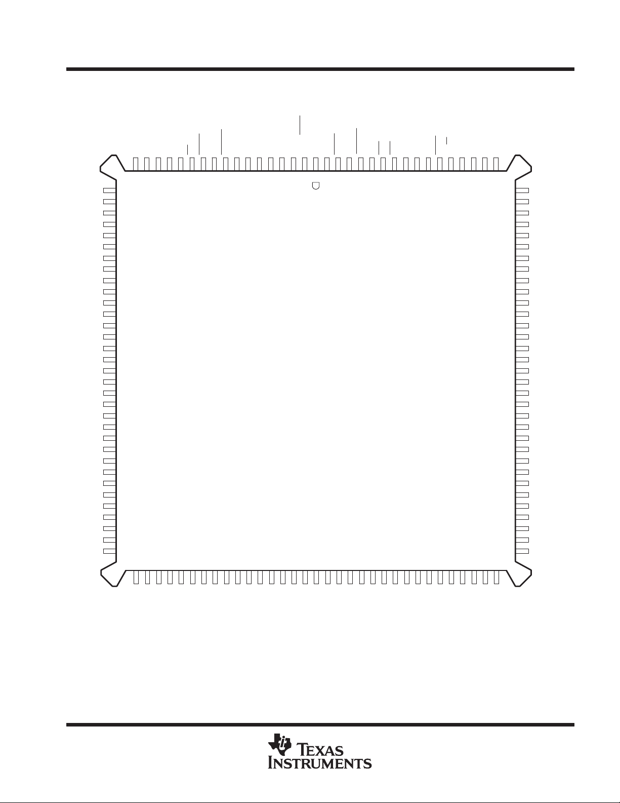
PQ PACKAGE
(TOP VIEW)
NC
B35
B34
B33
B32
GND
B31
B30
B29
B28
B27
B26
V
CC
B25
B24
GND
B23
B22
B21
B20
B19
B18
GND
B17
B16
V
CC
B15
B14
B13
B12
GND
NC
NC
CC
NCNCV
17 16 15 14 13 12 11 10 9 8 7 6 5 4 3 2
18
19
20
21
22
23
24
25
26
27
28
29
30
31
32
33
34
35
36
37
38
39
40
41
42
43
44
45
46
47
48
49
50
CLKB
5251 83828180797877767574737271706968676665646362616059585756555453
ENB
CSB
W/RB
GND
MBF1
GND
MBB
NC
V
CC
RFM
RTM
FS1/SEN
1
FS0/SD
GND
RST
132
131
130
MBA
129
CC
V
MBF2AEAF
126
128
127
125
CC
V
124
ORIRCSA
122
121
123
W/RA
ENA
120
119
CLKA
GND
118
117
NC
116
115
114
113
112
111
110
109
108
107
106
105
104
103
102
101
100
99
98
97
96
95
94
93
92
91
90
89
88
87
86
85
84
NC
NC
A35
A34
A33
A32
V
CC
A31
A30
GND
A29
A28
A27
A26
A25
A24
A23
GND
A22
V
CC
A21
A20
A19
A18
GND
A17
A16
A15
A14
A13
V
CC
A12
NC
B1 1
B9B8B7
B10
NC
NC – No internal connection
†
Uses Yamaichi socket IC51-1324-828
V
CC
B6
B5B4B3B2B1
GND
POST OFFICE BOX 655303 • DALLAS, TEXAS 75265
B0
A0A1A2
GND
CC
A3A4A5
V
A6A7A8
GND
A9
A10
A1 1
NC
GND
NC
3
SN74ACT3631
512 × 36
CLOCKED FIRST-IN, FIRST-OUT MEMORY
SCAS246G – AUGUST 1993 – REVISED APRIL 1998
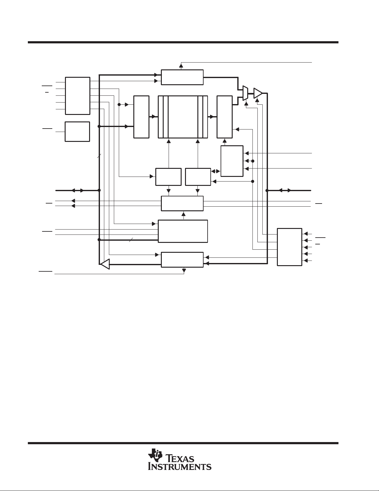
functional block diagram
CLKA
CSA
W/RA
ENA
MBA
RST
Port-A
Control
Logic
Reset
Logic
Input Register
MBF1
Mail1
Register
512 × 36
SRAM
Output Register
A0–A35
AF
FS0/SD
FS1/SEN
MBF2
36
Logic
Synch
Write
Pointer
IR
10
Status-Flag
Flag-Offset
Register
Register
Read
Pointer
Logic
Mail2
Retransmit
Port-B
Control
Logic
RTM
RFM
B0–B35
OR
AE
CLKB
CSB
W/RB
ENB
MBB
4
POST OFFICE BOX 655303 • DALLAS, TEXAS 75265
SN74ACT3631
512 × 36
CLOCKED FIRST-IN, FIRST-OUT MEMORY
SCAS246G – AUGUST 1993 – REVISED APRIL 1998
Terminal Functions
TERMINAL
NAME
A0–A35 I/O Port-A data. The 36-bit bidirectional data port for side A.
AE O
AF O
B0–B35 I/O Port-B data. The 36-bit bidirectional data port for side B.
CLKA I
CLKB I
CSA I
CSB I
ENA I Port-A master enable. ENA must be high to enable a low-to-high transition of CLKA to read or write data on port A.
ENB I Port-B master enable. ENB must be high to enable a low-to-high transition of CLKB to read or write data on port B.
FS1/SEN,
FS0/SD
IR O
MBA I Port-A mailbox select. A high level on MBA chooses a mailbox register for a port-A read or write operation.
MBB I
MBF1 O
MBF2 O
OR O
RFM I
RST I
RTM I
I/O DESCRIPTION
Almost-empty flag. Programmable flag synchronized to CLKB. AE is low when the number of words in the FIFO is less
than or equal to the value in the almost-empty offset register (X).
Almost-full flag. Programmable flag synchronized to CLKA. AF is low when the number of empty locations in the FIFO
is less than or equal to the value in the almost-full offset register (Y).
Port-A clock. CLKA is a continuous clock that synchronizes all data transfers through port A and can be asynchronous
or coincident to CLKB. IR and AF
Port-B clock. CLKB is a continuous clock that synchronizes all data transfers through port B and can be asynchronous
or coincident to CLKA. OR and AE
Port-A chip select. CSA must be low to enable a low-to-high transition of CLKA to read or write data on port A. The
A0–A35 outputs are in the high-impedance state when CSA
Port-B chip select. CSB must be low to enable a low-to-high transition of CLKB to read or write data on port B. The
B0–B35 outputs are in the high-impedance state when CSB
Flag offset select 1/serial enable, flag offset select 0/serial data. FS1/SEN and FS0/SD are dual-purpose inputs used
for flag offset register programming. During a device reset, FS1/SEN
method. Three offset register programming methods are available: automatically load one of two preset values, parallel
load from port A, and serial load.
I
When serial load is selected for flag offset register programming, FS1/SEN
low-to-high transition of CLKA. When FS1/SEN
X- and Y -offset registers. The number of bit writes required to program the offset register is 18. The first bit write stores
the Y-register MSB and the last bit write stores the X-register LSB.
Input-ready flag. IR is synchronized to the low-to-high transition of CLKA. When IR is low, the FIFO is full and writes
to its array are disabled. When the FIFO is in retransmit mode, IR indicates when the memory has been filled to the
point of the retransmit data and prevents further writes. IR is set low during reset and is set high after reset.
Port-B mailbox select. A high level on MBB chooses a mailbox register for a port-B read or write operation. When the
B0–B35 outputs are active, a high level on MBB selects data from the mail1 register for output and a low level selects
FIFO data for output.
Mail1 register flag. MBF1 is set low by the low-to-high transition of CLKA that writes data to the mail1 register . MBF1
is set high by a low-to-high transition of CLKB when a port-B read is selected and MBB is high. MBF1 is set high by
a reset.
Mail2 register flag. MBF2 is set low by the low-to-high transition of CLKB that writes data to the mail2 register . MBF2
is set high by a low-to-high transition of CLKA when a port-A read is selected and MBA is high. MBF2 is set high by
a reset.
Output-ready flag. OR is synchronized to the low-to-high transition of CLKB. When OR is low, the FIFO is empty and
reads are disabled. Ready data is present in the output register of the FIFO when OR is high. OR is forced low during
the reset and goes high on the third low-to-high transition of CLKB after a word is loaded to empty memory.
Read from mark. When the FIFO is in retransmit mode, a high on RFM enables a low-to-high transition of CLKB to reset
the read pointer to the beginning retransmit location and output the first selected retransmit data.
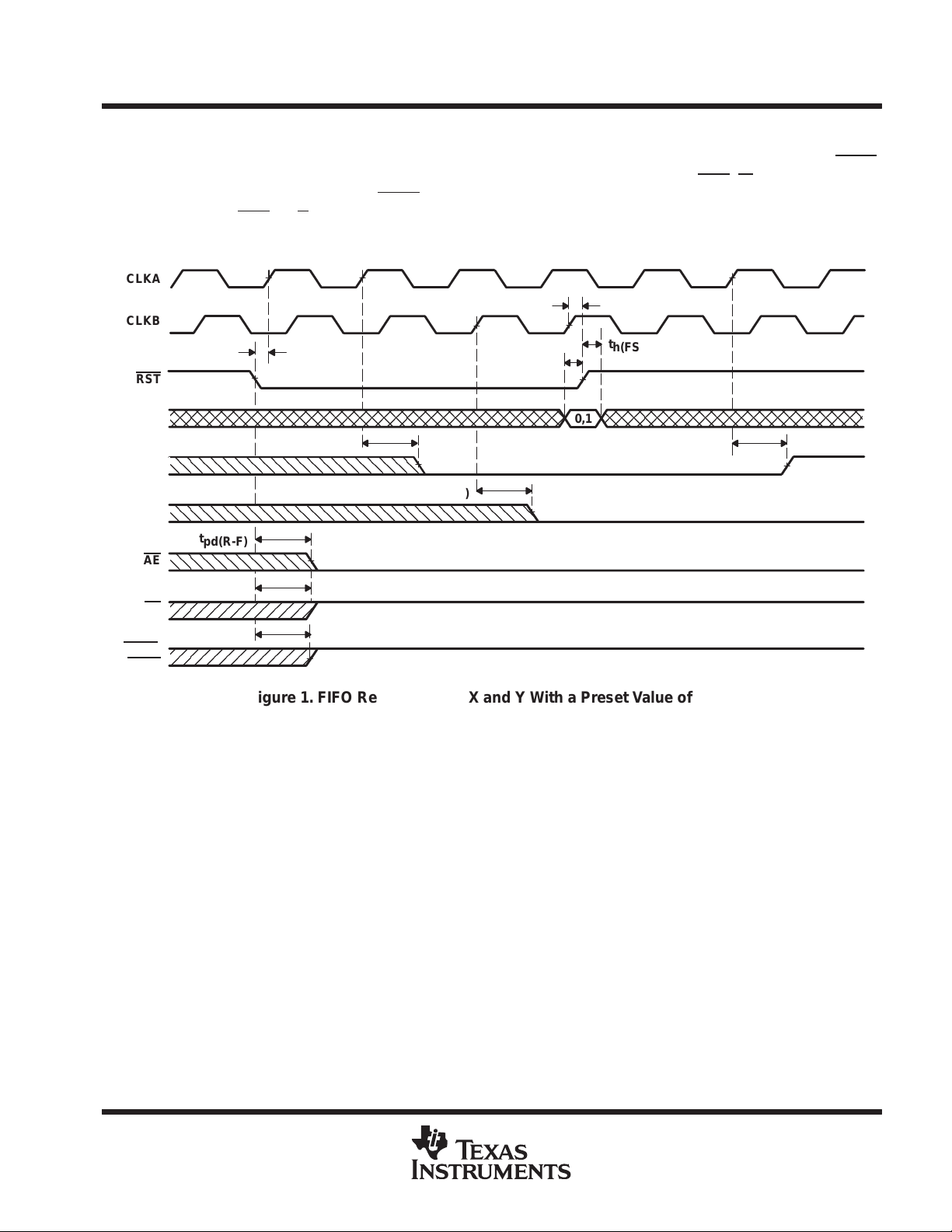
Reset. To reset the device, four low-to-high transitions of CLKA and four low-to-high transitions of CLKB must occur
while RST
Retransmit mode. When RTM is high and valid data is present in the FIFO output register (OR is high), a low-to-high
transition of CLKB selects the data for the beginning of a retransmit and puts the FIFO in retransmit mode. The selected
word remains the initial retransmit point until a low-to-high transition of CLKB occurs while RTM is low , taking the FIFO
out of retransmit mode.
is low. The low-to-high transition of RST latches the status of FS0 and FS1 for AF and AE offset selection.
are synchronous to the low-to-high transition of CLKA.
are synchronous to the low-to-high transition of CLKB.
is high.
is high.
and FS0/SD select the flag offset programming
is used as an enable synchronous to the
is low, a rising edge on CLKA loads the bit present on FS0/SD into the
POST OFFICE BOX 655303 • DALLAS, TEXAS 75265
5
SN74ACT3631
512 × 36
CLOCKED FIRST-IN, FIRST-OUT MEMORY
SCAS246G – AUGUST 1993 – REVISED APRIL 1998
Terminal Functions (Continued)
TERMINAL
NAME
W/RA I
W/RB I
I/O DESCRIPTION
Port-A write/read select. A high on W/RA selects a write operation and a low selects a read operation on port A for a
low-to-high transition of CLKA. The A0–A35 outputs are in the high-impedance state when W/R
Port-B write/read select. A low on W/RB selects a write operation and a high selects a read operation on port B for a
low-to-high transition of CLKB. The B0–B35 outputs are in the high-impedance state when W
A is high.
/RB is low.
detailed description
reset
The SN74ACT3631 is reset by taking the reset (RST
port-B clock (CLKB) low-to-high transitions. The reset input can switch asynchronously to the clocks. A reset
initializes the memory read and write pointers and forces the input-ready (IR) flag low, the output-ready (OR)
flag high, the almost-empty (AE
the mailbox flags (MBF1
, MBF2) high. After a FIFO is reset, its input-ready flag is set high after at least two clock
) flag low, and the almost-full (AF) flag high. Resetting the device also forces
cycles to begin normal operation. A FIFO must be reset after power up before data is written to its memory.
almost-empty flag and almost-full flag offset programming
Two registers in the SN74ACT3631 are used to hold the of fset values for the almost-empty and almost-full flags.
The almost-empty (AE
) flag offset register is labeled X, and the almost-full (AF) flag of fset register is labeled Y.
The offset registers can be loaded with a value in three ways: one of two preset values is loaded into the offset
registers, parallel load from port A, or serial load. The offset register programming mode is chosen by the flag
select (FS1, FS0) inputs during a low-to-high transition on the RST
) input low for at least four port-A clock (CLKA) and four
input (see Table 1).
Table 1. Flag Programming
FS1 FS0 RST
H H ↑ Serial load
H L ↑ 64
L H ↑ 8
L L ↑ Parallel load from port A
†
X register holds the offset for AE
offset for AF
.
X AND Y REGISTERS
; Y register holds the
†
preset values
If a preset value of 8 or 64 is chosen by FS1 and FS0 at the time of a RST low-to-high transition according to
Table 1, the preset value is automatically loaded into the X and Y registers. No other device initialization is
necessary to begin normal operation, and the IR flag is set high after two low-to-high transitions on CLKA.
parallel load from port A
To program the X and Y registers from port A, the device is reset with FS0 and FS1 low during the low-to-high
transition of RST
. After this reset is complete, the IR flag is set high after two low-to-high transitions on CLKA.
The first two writes to the FIFO do not store data in its memory but load the offset registers in the order Y, X.
Each offset register of the SN74ACT3631 uses port-A inputs (A8 –A0). The highest number input is used as
the most-significant bit of the binary number in each case. Each register value can be programmed from 1 to
508. After both offset registers are programmed from port A, subsequent FIFO writes store data in the SRAM.
6
POST OFFICE BOX 655303 • DALLAS, TEXAS 75265
SN74ACT3631
CLOCKED FIRST-IN, FIRST-OUT MEMORY
SCAS246G – AUGUST 1993 – REVISED APRIL 1998
serial load
To serially program the X and Y registers, the device is reset with FS0/SD and FS1/SEN high during the
low-to-high transition of RST
FS0/SD on each low-to-high transition of CLKA that FS1/SEN
the programming. The first bit write stores the most-significant bit of the Y register, and the last bit write stores
the least-significant bit of the X register. Each register value can be programmed from 1 to 508.
When the option to program the offset registers serially is chosen, the input-ready (IR) flag remains low until
all register bits are written. The IR flag is set high by the low-to-high transition of CLKA after the last bit is loaded
to allow normal FIFO operation.
FIFO write/read operation
. After this reset is complete, the X- and Y -register values are loaded bitwise through
is low. W rites of 18 bits are needed to complete
512 × 36
The state of the port-A data (A0 –A35) outputs is controlled by the port-A chip select (CSA
write/read select (W/R
high. The A0–A35 outputs are active when both CSA
A). The A0–A35 outputs are in the high-impedance state when either CSA or W/RA is
and W/RA are low.
Data is loaded into the FIFO from the A0–A35 inputs on a low-to-high transition of CLKA when CSA
port-A mailbox select (MBA) are low, W/R
A, the port-A enable (ENA), and the input-ready (IR) flag are high
) and the port-A
and the
(see Table 2). Writes to the FIFO are independent of any concurrent FIFO reads.
Table 2. Port-A Enable Function Table
CSA W/RA ENA MBA CLKA
H X X X X In high-impedance state None
L H L X X In high-impedance state None
L H H L ↑ In high-impedance state FIFO write
L H H H ↑ In high-impedance state Mail1 write
L L L L X Active, mail2 register None
L L H L ↑ Active, mail2 register None
L L L H X Active, mail2 register None
L L H H ↑ Active, mail2 register Mail2 read (set MBF2 high)
A0–A35 OUTPUTS PORT FUNCTION
The port-B control signals are identical to those of port A, with the exception that the port-B write/read select
(W
/RB) is the inverse of the port-A write/read select (W/RA). The state of the port-B data (B0–B35) outputs is
controlled by the port-B chip select (CSB
in the high-impedance state when either CSB
) and the port-B write/read select (W/RB). The B0–B35 outputs are
is high or W/RB is low. The B0–B35 outputs are active when CSB
is low and W/RB is high.
Data is read from the FIFO to its output register on a low-to-high transition of CLKB when CSB
mailbox select (MBB) are low, W
/RB, the port-B enable (ENB), and the output-ready (OR) flag are high
(see Table 3). Reads from the FIFO are independent of any concurrent FIFO writes.
POST OFFICE BOX 655303 • DALLAS, TEXAS 75265
and the port-B
7
SN74ACT3631
FIFO
†‡
512 × 36
CLOCKED FIRST-IN, FIRST-OUT MEMORY
SCAS246G – AUGUST 1993 – REVISED APRIL 1998
FIFO write/read operation (continued)
Table 3. Port-B Enable Function Table
CSB W/RB ENB MBB CLKB
H X X X X In high-impedance state None
L L L X X In high-impedance state None
L L H L ↑ In high-impedance state None
L L H H ↑ In high-impedance state Mail2 write
L H L L X Active, FIFO output register None
L H H L ↑ Active, FIFO output register FIFO read
L H L H X Active, mail1 register None
L H H H ↑ Active, mail1 register Mail1 read (set MBF1 high)
B0–B35 OUTPUTS PORT FUNCTION
The setup- and hold-time constraints to the port clocks for the port-chip selects and write/read selects are only
for enabling write and read operations and are not related to high-impedance control of the data outputs. If a
port enable is low during a clock cycle, the port-chip select and write/read select can change states during the
setup- and hold-time window of the cycle.
When the output-ready (OR) flag is low, the next data word is sent to the FIFO output register automatically by
the CLKB low-to-high transition that sets the output-ready flag high. When OR is high, an available data word
is clocked to the FIFO output register only when a FIFO read is selected by the port-B chip select (CSB
write/read select (W
/RB), enable (ENB), and mailbox select (MBB).
synchronized FIFO flags
Each FIFO flag is synchronized to its port clock through at least two flip-flop stages. This is done to improve the
flags’ reliability by reducing the probability of metastable events on their outputs when CLKA and CLKB operate
asynchronously to one another .
OR and AE are synchronized to CLKB. IR and AF are synchronized to CLKA.
Table 4 shows the relationship of each flag to the number of words stored in memory.
),
Table 4. FIFO Flag Operation
NUMBER OF WORDS IN
0 L L H H
1 to X H LHH
(X + 1) to [512 – (Y + 1)] H HHH
(512 – Y) to 511 H HLH
512 H H L L
†
X is the almost-empty offset for AE. Y is the almost-full offset for AF.
‡
When a word is present in the FIFO output register, its previous memory
location is free.
SYNCHRONIZED
TO CLKB
OR AE AF IR
SYNCHRONIZED
TO CLKA
8
POST OFFICE BOX 655303 • DALLAS, TEXAS 75265

SN74ACT3631
CLOCKED FIRST-IN, FIRST-OUT MEMORY
SCAS246G – AUGUST 1993 – REVISED APRIL 1998
output-ready flag (OR)
The output-ready flag of a FIFO is synchronized to the port clock that reads data from its array (CLKB). When
the output-ready flag is high, new data is present in the FIFO output register. When the output-ready flag is low ,
the previous data word is present in the FIFO output register and attempted FIFO reads are ignored.
A FIFO read pointer is incremented each time a new word is clocked to its output register. From the time a word
is written to a FIFO, it can be shifted to the FIFO output register in a minimum of three cycles of CLKB; therefore,
an output-ready flag is low if a word in memory is the next data to be sent to the FIFO output register and three
CLKB cycles have not elapsed since the time the word was written. The output-ready flag of the FIFO remains
low until the third low-to-high transition of CLKB occurs, simultaneously forcing the output-ready flag high and
shifting the word to the FIFO output register.
A low-to-high transition on CLKB begins the first synchronization cycle of a write if the clock transition
occurs at time t
synchronization cycle (see Figure 6).
input-ready flag (IR)
The input-ready flag of a FIFO is synchronized to the port clock that writes data to its array (CLKA). When the
input-ready flag is high, a memory location is free in the SRAM to write new data. No memory locations are free
when the input-ready flag is low and attempted writes to the FIFO are ignored.
, or greater, after the write. Otherwise, the subsequent CLKB cycle can be the first
sk(1)
512 × 36
Each time a word is written to a FIFO, its write pointer is incremented. From the time a word is read from a FIFO,
its previous memory location is ready to be written in a minimum of three cycles of CLKA; therefore, an
input-ready flag is low if less than two cycles of CLKA have elapsed since the next memory write location has
been read. The second low-to-high transition on CLKA after the read sets the input-ready flag high, and data
can be written in the following cycle.
A low-to-high transition on CLKA begins the first synchronization cycle of a read if the clock transition
occurs at time t
synchronization cycle (see Figure 7).
, or greater, after the read. Otherwise, the subsequent CLKA cycle can be the first
sk(1)
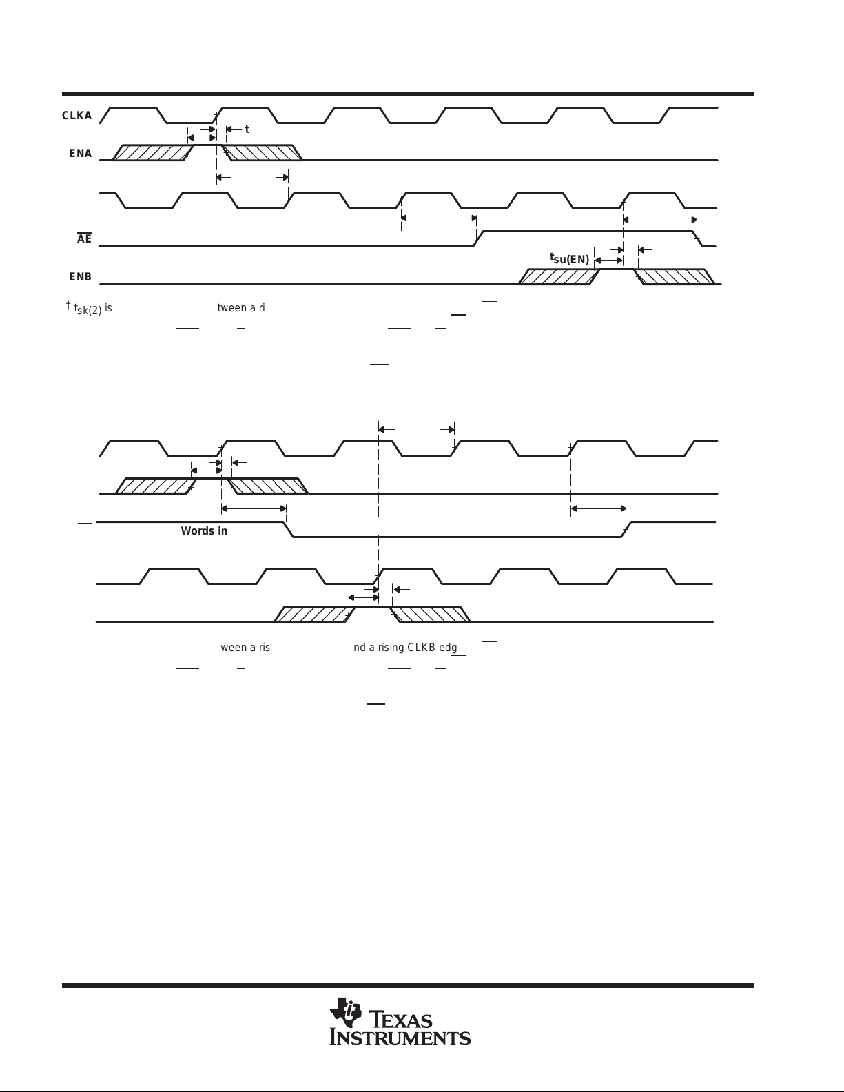
almost-empty flag (AE)
The almost-empty flag of a FIFO is synchronized to the port clock that reads data from its array (CLKB). The
almost-empty state is defined by the contents of register X. This register is loaded with a preset value during
a FIFO reset, programmed from port A, or programmed serially (see
programming
FIFO contains (X + 1) or more words. A data word present in the FIFO output register has been read from
memory.
Two low-to-high transitions of CLKB are required after a FIFO write for the almost-empty flag to reflect the new
level of fill; therefore, the almost-empty flag of a FIFO containing (X + 1) or more words remains low if two cycles
of CLKB have not elapsed since the write that filled the memory to the (X + 1) level. An almost-empty flag is set
high by the second low-to-high transition of CLKB after the FIFO write that fills memory to the (X + 1) level.
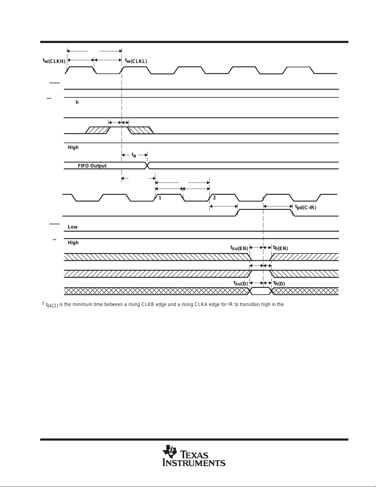
A low-to-high transition of CLKB begins the first synchronization cycle if it occurs at time t
the write that fills the FIFO to (X + 1) words. Otherwise, the subsequent CLKB cycle can be the first
synchronization cycle (see Figure 8).
). The almost-empty flag is low when the FIFO contains X or fewer words and is high when the
almost-empty flag and almost-full flag offset
, or greater, after
sk(2)
almost-full flag (AF)
The almost-full flag of a FIFO is synchronized to the port clock that writes data to its array (CLKA). The almost-full
state is defined by the contents of register Y. This register is loaded with a preset value during a FIFO reset,
programmed from port A, or programmed serially (see
programming
(512 – Y). The almost-full flag is high when the number of words in the FIFO is less than or equal to
[512 – (Y + 1)]. A data word present in the FIFO output register has been read from memory.
). The almost-full flag is low when the number of words in the FIFO is greater than or equal to
POST OFFICE BOX 655303 • DALLAS, TEXAS 75265
almost-empty flag and almost-full flag offset
9

SN74ACT3631
512 × 36
CLOCKED FIRST-IN, FIRST-OUT MEMORY
SCAS246G – AUGUST 1993 – REVISED APRIL 1998
Two low-to-high transitions of CLKA are required after a FIFO read for its almost-full flag to reflect the new level
of fill; therefore, the almost-full flag of a FIFO containing [512 – (Y + 1)] or fewer words remains low if two cycles
of CLKA have not elapsed since the read that reduced the number of words in memory to [512 – (Y + 1)]. An
almost-full flag is set high by the second low-to-high transition of CLKA after the FIFO read that reduces the
number of words in memory to [512 – (Y + 1)]. A low-to-high transition of CLKA begins the first synchronization
cycle if it occurs at time t
[512 – (Y + 1)]. Otherwise, the subsequent CLKA cycle can be the first synchronization cycle (see Figure 9).
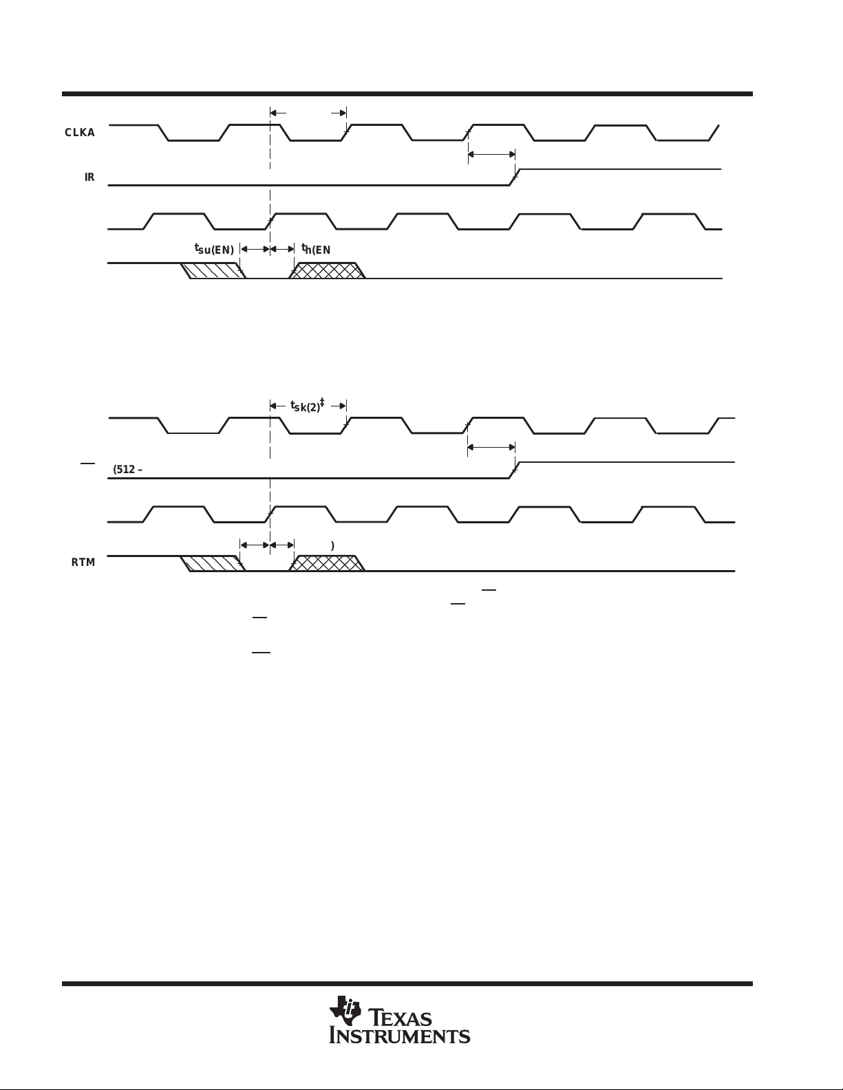
synchronous retransmit
The synchronous-retransmit feature of the SN74ACT3631 allows FIFO data to be read repeatedly starting at
a user-selected position. The FIFO is first put into retransmit mode to select a beginning word and prevent
ongoing FIFO write operations from destroying retransmit data. Data vectors with a minimum length of three
words can retransmit repeatedly starting at the selected word. The FIFO can be taken out of retransmit mode
at any time and allow normal device operation.
The FIFO is put in retransmit mode by a low-to-high transition on CLKB when the retransmit-mode (RTM) input
is high and OR is high. This rising CLKB edge marks the data present in the FIFO output register as the first
retransmit data. The FIFO remains in retransmit mode until a low-to-high transition occurs while RTM is low.
When two or more reads occur after the initial retransmit word, a retransmit is initiated by a low-to-high transition
on CLKB when the read-from-mark (RFM) input is high. This rising CLKB edge shifts the first retransmit word
to the FIFO output register and subsequent reads can begin immediately. Retransmit loops can be done
endlessly while the FIFO is in retransmit mode. RFM must be low during the CLKB rising edge that takes the
FIFO out of retransmit mode.
, or greater, after the read that reduces the number of words in memory to
sk(2)
When the FIFO is put into retransmit mode, it operates with two read pointers. The current read pointer operates
normally , incrementing each time a new word is shifted to the FIFO output register and used by the OR and AE
flags. The shadow read pointer stores the SRAM location at the time the device is put into retransmit mode and
does not change until the device is taken out of retransmit mode. The shadow read pointer is used by the IR
and AF
stores (512 – Y) words after the first retransmit word. The IR flag is set low by the 512th write after the first
retransmit word.
When the FIFO is in retransmit mode and RFM is high, a rising CLKB edge loads the current read pointer with
the shadow read-pointer value and the OR flag reflects the new level of fill immediately . If the retransmit changes
the FIFO status out of the almost-empty range, up to two CLKB rising edges after the retransmit cycle are
needed to switch AE
shifts the read pointer used by the IR and AF
of read pointer used by IR and AF
synchronizing cycles are needed before the flags reflect the change. A rising CLKA edge after the FIFO is taken
out of retransmit mode is the first synchronizing cycle of IR if it occurs at time t
CLKB edge (see Figure 12). A rising CLKA edge after the FIFO is taken out of retransmit mode is the first
synchronizing cycle of AF
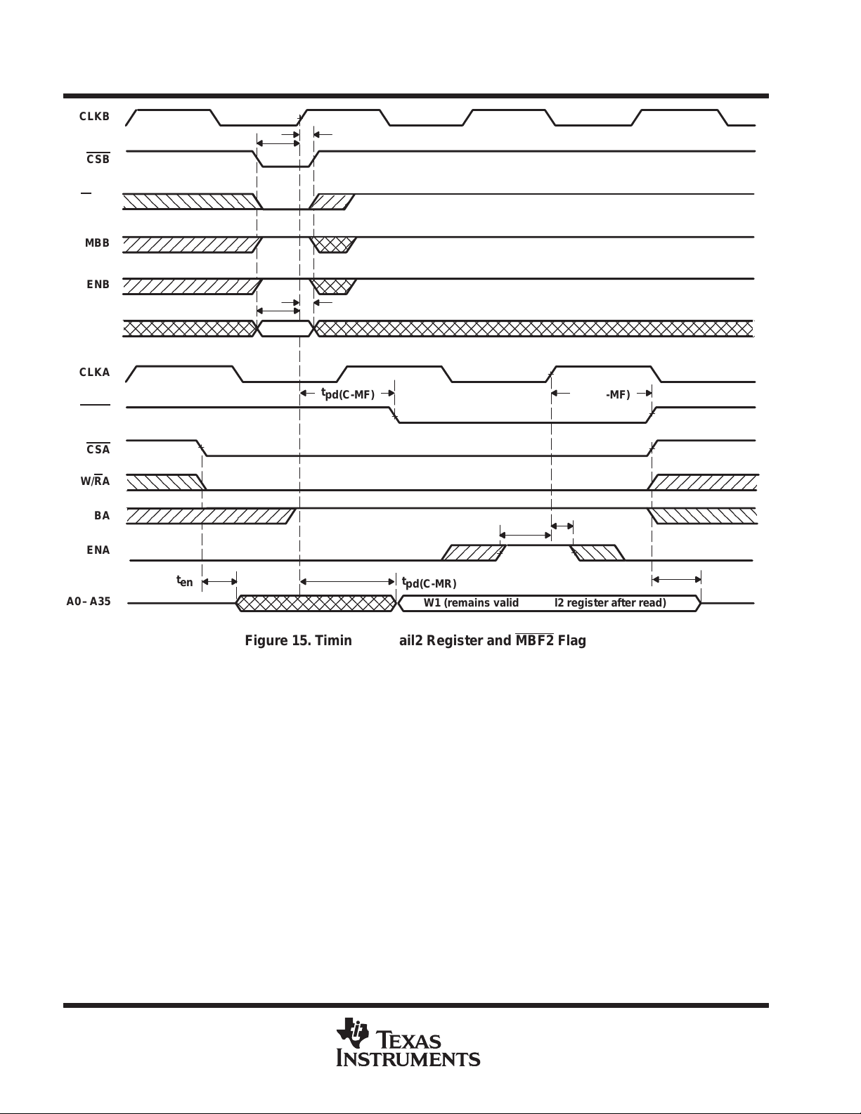
mailbox registers
Two 36-bit bypass registers pass command and control information between port A and port B. The
mailbox-select (MBA, MBB) inputs choose between a mail register and a FIFO for a port data transfer operation.
A low-to-high transition on CLKA writes A0–A35 data to the mail1 register when a port-A write is selected by
CSA
when a port-B write is selected by CSB
corresponding flag (MBF1
low.
flags. Data writes can proceed while the FIFO is in retransmit mode, but AF is set low by the write that
high (see Figure 11). The rising CLKB edge that takes the FIFO out of retransmit mode
flags from the shadow to the current read pointer. If the change
should cause one or both flags to transition high, at least two CLKA
, or greater, after the rising
sk(1)
if it occurs at time t
, W/RA, and ENA with MBA high. A low-to-high transition on CLKB writes B0–B35 data to the mail2 register
, W/RB, and ENB with MBB high. Writing data to a mail register sets its
or MBF2) low. Attempted writes to a mail register are ignored while its mail flag is
, or greater, after the rising CLKB edge (see Figure 14).
sk(2)
10
POST OFFICE BOX 655303 • DALLAS, TEXAS 75265
SN74ACT3631
CLOCKED FIRST-IN, FIRST-OUT MEMORY
SCAS246G – AUGUST 1993 – REVISED APRIL 1998
When the port-B data (B0–B35) outputs are active, the data on the bus comes from the FIFO output register
when the port-B mailbox select (MBB) input is low and from the mail1 register when MBB is high. Mail2 data
is always present on the port-A data (A0–A35) outputs when they are active. The mail1 register flag (MBF1
is set high by a low-to-high transition on CLKB when a port-B read is selected by CSB
MBB high. The mail2 register flag (MBF2
is selected by CSA
, W/RA, and ENA with MBA high. The data in a mail register remains intact after it is read
) is set high by a low-to-high transition on CLKA when a port-A read
and changes only when new data is written to the register.
CLKA
t
CLKB
RST
t
su(RS)
t
su(FS)
h(RS)
t
h(FS)
, W/RB, and ENB with
512 × 36
)
FS1, FS0
OR
AE
AF
MBF1,
MBF2
0,1
t
pd(C-IR)
IR
t
pd(C-OR)
t
pd(R-F)
t
pd(R-F)
t
pd(R-F)
t
pd(C-IR)
Figure 1. FIFO Reset Loading X and Y With a Preset Value of Eight
POST OFFICE BOX 655303 • DALLAS, TEXAS 75265
11

SN74ACT3631
512 × 36
CLOCKED FIRST-IN, FIRST-OUT MEMORY
SCAS246G – AUGUST 1993 – REVISED APRIL 1998
CLKA
RST
t
su(FS)
FS1, FS0
IR
ENA
A0–A35
NOTE A: CSA = L, W/RA = H, MBA = L. It is not necessary to program offset register bits on consecutive clock cycles.
4
t
h(FS)
t
pd(C-IR)
t
h(EN)
First Word Stored in FIFO
t
su(D)
AF Offset
(Y)
t
su(EN)
t
h(D)
AE Offset
(X)
Figure 2. Programming the AF Flag and AE Flag Offset Values From Port A
CLKA
4
RST
t
pd(C-IR)
IR
t
t
h(FS)
h(SP)
t
su(SEN)
t
su(SD)
AF Offset
(Y) MSB
t
su(FS)
FS1/SEN
t
su(FS)
FS0/SD
NOTE A: It is not necessary to program offset register bits on consecutive clock cycles. FIFO write attempts are ignored until IR is set high.
t
h(SEN)
t
h(SD)
t
su(SEN)
t
su(SD)
AE Offset
(X) LSB
t
h(SEN)
t
h(SD)
Figure 3. Serially Programming the AF Flag and AE Flag Offset Values
12
POST OFFICE BOX 655303 • DALLAS, TEXAS 75265

ÎÎÎ
ООООООО
t
w(CLKH)
CLKA
CSA
W/RA
MBA
ENA
A0–A35
SN74ACT3631
512 × 36
CLOCKED FIRST-IN, FIRST-OUT MEMORY
SCAS246G – AUGUST 1993 – REVISED APRIL 1998
t
c
t
w(CLKL)
IR
High
t
su(EN)
t
su(EN)
t
su(EN)
t
su(EN)
t
su(D)
W1
t
h(EN)
t
h(EN)
t
h(EN)
t
h(EN)
t
h(D)
t
su(EN)
W2
t
h(EN)
t
su(EN)
No Operation
t
h(EN)
t
w(CLKH)
CLKB
OR
CSB
W/RB
MBB
ENB
B0–B35
High
t
pd(M-DV)
Figure 4. FIFO Write-Cycle Timing
t
c
t
w(CLKL)
t
su(EN)
t
h(EN)
W1
t
a
t
en
t
su(EN)
W2
t
h(EN)
t
a
t
su(EN)
Operation
W3
No
t
h(EN)
t
dis
Figure 5. FIFO Read-Cycle Timing
POST OFFICE BOX 655303 • DALLAS, TEXAS 75265
13

SN74ACT3631
512 × 36
CLOCKED FIRST-IN, FIRST-OUT MEMORY
SCAS246G – AUGUST 1993 – REVISED APRIL 1998
t
w(CLKH)
CLKA
Low
CSA
t
c
t
w(CLKL)
W/RA
MBA
ENA
A0–A35
CLKB
OR
CSB
W/RB
MBB
ENB
B0–B35
High
t
su(EN)
t
su(EN)
High
IR
Low
High
Low
t
su(D)
W1
†
t
sk(1)
t
Old Data in FIFO Output Register
t
h(EN)
t
h(EN)
t
h(D)
w(CLKH)
123
Old Data in FIFO Output Register
t
c
t
w(CLKL)
t
pd(C-OR)
t
su(EN)
t
a
t
h(EN)
t
pd(C-OR)
W1
†
t
is the minimum time between a rising CLKA edge and a rising CLKB edge for OR to transition high and to clock the next word to the FIFO
sk(1)
output register in three CLKB cycles. If the time between the rising CLKA edge and rising CLKB edge is less than t
OR high and the first word load to the output register can occur one CLKB cycle later than shown.
, then the transition of
sk(1)
Figure 6. OR-Flag Timing and First Data-Word Fall-Through When the FIFO Is Empty
14
POST OFFICE BOX 655303 • DALLAS, TEXAS 75265
(1)
t
w(CLKH)
CLKB
SN74ACT3631
512 × 36
CLOCKED FIRST-IN, FIRST-OUT MEMORY
SCAS246G – AUGUST 1993 – REVISED APRIL 1998
t
c
t
w(CLKL)
CSB
W/RB
MBB
ENB
OR
B0–B35
CLKA
CSA
W/RA
MBA
ENA
A0–A35
Low
High
Low
t
su(EN)
High
FIFO Output Register Next Word From FIFO
IR
Low
High
t
h(EN)
t
a
t
sk(1)
t
w(CLKH)
FIFO Full
†
12
t
c
t
pd(C-IR)
t
w(CLKL)
t
su(EN)
t
su(EN)
t
su(D)
Write
t
h(EN)
t
h(EN)
t
h(D)
t
pd(C-IR)
†
t
is the minimum time between a rising CLKB edge and a rising CLKA edge for IR to transition high in the next CLKA cycle. If the time
sk(1)
between the rising CLKB edge and rising CLKA edge is less than t
, then IR can transition high one CLKA cycle later than shown.
sk
Figure 7. IR-Flag Timing and First Available Write When the FIFO Is Full
POST OFFICE BOX 655303 • DALLAS, TEXAS 75265
15
SN74ACT3631
512 × 36
CLOCKED FIRST-IN, FIRST-OUT MEMORY
SCAS246G – AUGUST 1993 – REVISED APRIL 1998
CLKA
t
t
su(EN)
ENA
CLKB
X Words in FIFO
AE
ENB
†
t
is the minimum time between a rising CLKA edge and a rising CLKB edge for AE to transition high in the next CLKB cycle. If the time
sk(2)
between the rising CLKA edge and rising CLKB edge is less than t
NOTE A: FIFO write (CSA
CLKA
t
su(EN)
ENA
AF
[512 – (Y + 1)] Words in FIFO
= L, W/RA = H, MBA = L), FIFO read (CSB = L, W/RB = H, MBB = L)
t
pd(C-AF)
h(EN)
†
t
sk(2)
1
2
t
sk(2)
pd(C-AE)
, then AE
(X + 1) Words in FIFO
t
su(EN)
can transition high one CLKB cycle later than shown.
Figure 8. Timing for AE When FIFO Is Almost Empty
‡
t
sk(2)
t
h(EN)
(512 – Y) Words in FIFO
12
t
pd(C-AF)
t
pd(C-AE)
t
h(EN)
CLKB
t
sk(2)
h(EN)
, then AF
can transition high one CLKA cycle later than shown.
t
su(EN)
ENB
‡
t
is the minimum time between a rising CLKA edge and a rising CLKB edge for AF to transition high in the next CLKA cycle. If the time
sk(2)
between the rising CLKB edge and rising CLKA edge is less than t
NOTE A: FIFO write (CSA
= L, W/RA = H, MBA = L), FIFO read (CSB = L, W/RB = H, MBB = L)
Figure 9. Timing for AF When the FIFO Is Almost Full
16
POST OFFICE BOX 655303 • DALLAS, TEXAS 75265
CLKB
ENB
RTM
t
su(EN)
t
su(EN)
t
h(EN)
t
h(EN)
SN74ACT3631
CLOCKED FIRST-IN, FIRST-OUT MEMORY
SCAS246G – AUGUST 1993 – REVISED APRIL 1998
t
su(EN)
t
h(EN)
t
su(EN)
t
h(EN)
512 × 36
t
su(EN)
RFM
OR
High
t
a
B0–B35
NOTE A: CSB = L, W/RB = H, MBB = L. No input enables other than RTM and RFM are needed to control retransmit mode or begin a retransmit.
Other enables are shown only to relate retransmit operations to the FIFO output register.
W0 W1
Initiate Retransmit Mode
With W0 as First Word
t
a
W2
Retransmit From
Selected Position
t
t
a
h(EN)
t
a
W0
End Retransmit
Mode
W1
Figure 10. Retransmit Timing Showing Minimum Retransmit Length
CLKB
RTM
RFM
High
t
su(RM)
t
h(RM)
12
t
pd(C-AE)
AE
NOTE A: X is the value loaded in the AE flag offset register.
X or Fewer Words From Empty
(X + 1) or More Words From Empty
Figure 11. AE Maximum Latency When Retransmit Increases the Number of Stored Words Above X
POST OFFICE BOX 655303 • DALLAS, TEXAS 75265
17
SN74ACT3631
(1)
512 × 36
CLOCKED FIRST-IN, FIRST-OUT MEMORY
SCAS246G – AUGUST 1993 – REVISED APRIL 1998
†
t
sk(1)
CLKA
IR
CLKB
FIFO Filled to First Retransmit Word
12
t
pd(C-IR)
One or More Write Locations Available
t
su(EN)
RTM
†
t
is the minimum time between a rising CLKB edge and a rising CLKA edge for IR to transition high in the next CLKA cycle. If the time
sk(1)
between the rising CLKB edge and rising CLKA edge is less than t
t
h(EN)
, then IR can transition high one CLKA cycle later than shown.
sk
Figure 12. IR Timing From the End of Retransmit Mode When One or More Write Locations Are Available
‡
t
sk(2)
CLKA
(512 – Y) or More Words Past First Retransmit Word
AF
CLKB
t
su(EN)
RTM
‡
t
is the minimum time between a rising CLKB edge and a rising CLKA edge for AF
sk(2)
between the rising CLKB edge and rising CLKA edge is less than t
NOTE A: Y is the value loaded in the AF
t
h(EN)
flag offset register .
12
t
pd(C-AE)
(Y + 1) or More Write Locations Available
to transition high in the next CLKA cycle. If the time
can transition high one CLKA cycle later than shown.
sk(2)
, then AF
18
Figure 13. AF Timing From the End of Retransmit Mode When (Y + 1)
or More Write Locations Are Available
POST OFFICE BOX 655303 • DALLAS, TEXAS 75265

CLKA
CSA
W/RA
MBA
ENA
A0–A35
CLKB
MBF1
t
su(EN)
t
su(D)
W1
t
h(EN)
t
h(D)
t
pd(C-MF)
SN74ACT3631
512 × 36
CLOCKED FIRST-IN, FIRST-OUT MEMORY
SCAS246G – AUGUST 1993 – REVISED APRIL 1998
t
pd(C-MF)
CSB
W/RB
MBB
ENB
B0–B35
t
t
su(EN)
t
t
en
FIFO Output Register
pd(M-DV)
t
pd(C-MR)
W1 (remains valid in mail1 register after read)
h(EN)
t
dis
Figure 14. Timing for Mail1 Register and MBF1 Flag
POST OFFICE BOX 655303 • DALLAS, TEXAS 75265
19
SN74ACT3631
512 × 36
CLOCKED FIRST-IN, FIRST-OUT MEMORY
SCAS246G – AUGUST 1993 – REVISED APRIL 1998
CLKB
t
h(EN)
t
h(D)
t
pd(C-MF)
CSB
W/RB
MBB
ENB
B0–B35
CLKA
MBF2
t
su(EN)
t
su(D)
W1
t
pd(C-MF)
CSA
W/RA
MBA
ENA
A0–A35
t
t
su(EN)
t
en
t
pd(C-MR)
W1 (remains valid in mail2 register after read)
h(EN)
t
dis
Figure 15. Timing for Mail2 Register and MBF2 Flag
20
POST OFFICE BOX 655303 • DALLAS, TEXAS 75265
§
Other in uts at V
CC
GND
SN74ACT3631
512 × 36
CLOCKED FIRST-IN, FIRST-OUT MEMORY
SCAS246G – AUGUST 1993 – REVISED APRIL 1998
absolute maximum ratings over operating free-air temperature range (unless otherwise noted)
Supply voltage range, V
Input voltage range, V
Output voltage range, V
Input clamp current, I
Output clamp current, I
Continuous output current, I
Continuous current through V
Package thermal impedance,
Storage temperature range, T
†
Stresses beyond those listed under “absolute maximum ratings” may cause permanent damage to the device. These are stress ratings only, and
functional operation of the device at these or any other conditions beyond those indicated under “recommended operating conditions” is not
implied. Exposure to absolute-maximum-rated conditions for extended periods may affect device reliability.
NOTES: 1. The input and output voltage ratings can be exceeded provided the input and output current ratings are observed.
2. The package thermal impedance is calculated in accordance with JESD 51.
–0.5 V to 7 V. . . . . . . . . . . . . . . . . . . . . . . . . . . . . . . . . . . . . . . . . . . . . . . . . . . . . . . . . .
CC
(see Note 1) –0.5 V to VCC + 0.5 V. . . . . . . . . . . . . . . . . . . . . . . . . . . . . . . . . . . . . . . . . .
I
(see Note 1) –0.5 V to VCC + 0.5 V. . . . . . . . . . . . . . . . . . . . . . . . . . . . . . . . . . . . . . . .
O
(VI < 0 or VI > VCC) ±20 mA. . . . . . . . . . . . . . . . . . . . . . . . . . . . . . . . . . . . . . . . . . . . . . . .
IK
(VO < 0 or VO > VCC) ±50 mA. . . . . . . . . . . . . . . . . . . . . . . . . . . . . . . . . . . . . . . . . . . .
OK
(VO = 0 to VCC) ±50 mA. . . . . . . . . . . . . . . . . . . . . . . . . . . . . . . . . . . . . . . . . . . . . .
O
or GND ±400 mA. . . . . . . . . . . . . . . . . . . . . . . . . . . . . . . . . . . . . . . . . . . . . . . . . .
CC
q
(see Note 2): PCB package 28°C/W. . . . . . . . . . . . . . . . . . . . . . . . . . . . . . . .
JA
PQ package 46°C/W. . . . . . . . . . . . . . . . . . . . . . . . . . . . . . . . .
–65°C to 150°C. . . . . . . . . . . . . . . . . . . . . . . . . . . . . . . . . . . . . . . . . . . . . . . . . . .
stg
recommended operating conditions
MIN MAX UNIT
V
V
V
I
OH
I
OL
T
CC
IH
IL
A
Supply voltage 4.5 5.5 V
High-level input voltage 2 V
Low-level input voltage 0.8 V
High-level output current –4 mA
Low-level output current 8 mA
Operating free-air temperature 0 70 °C
†
electrical characteristics over recommended operating free-air temperature range (unless
otherwise noted)
PARAMETER TEST CONDITIONS MIN TYP‡MAX UNIT
V
OH
V
OL
I
I
I
OZ
I
CC
∆I
CC
C
i
C
‡
All typical values are at VCC = 5 V, TA = 25°C.
§
This is the supply current when each input is at one of the specified TTL voltage levels rather than 0 V or VCC.
o
VCC = 4.5 V, IOH = –4 mA 2.4 V
VCC = 4.5 V, IOL = 8 mA 0.5 V
VCC = 5.5 V, VI = VCC or 0 ±5 µA
VCC = 5.5 V, VO = VCC or 0 ±5 µA
VCC = 5.5 V, VI = VCC – 0.2 V or 0 400 µA
CSA = V
VCC = 5.5 V, One input at 3.4 V,
p
VI = 0, f = 1 MHz 4 pF
VO = 0, f = 1 MHz 8 pF
or
CSB = V
CSA = V
CSB = V
All other inputs 1
A0–A35 0
IH
B0–B35 0
IH
A0–A35 1
IL
B0–B35 1
IL
mA
POST OFFICE BOX 655303 • DALLAS, TEXAS 75265
21

SN74ACT3631
UNIT
512 × 36
CLOCKED FIRST-IN, FIRST-OUT MEMORY
SCAS246G – AUGUST 1993 – REVISED APRIL 1998
timing requirements over recommended ranges of supply voltage and operating free-air
temperature (see Figures 1 through 16)
’ACT3631-15 ’ACT3631-20 ’ACT3631-30
MIN MAX MIN MAX MIN MAX
f
clock
t
c
t
w(CH)
t
w(CL)
t
su(D)
t
su(SEN)
t
su(EN2)
t
su(RM)
t
su(RS)
t
su(FS)
t
su(SD)
t
su(EN1)
t
h(D)
t
h(EN1)
t
h(EN2)
t
h(RM)
t
h(RS)
t
h(FS)
t
h(SP)
t
h(SD)
t
h(SEN)
t
sk(1)
t
sk(2)
†
Requirement to count the clock edge as one of at least four needed to reset a FIFO
‡
Applies only when serial load method is used to program flag offset registers
§
Skew time is not a timing constraint for proper device operation and is included to illustrate the timing relationship between CLKA cycle and CLKB
cycle.
Clock frequency, CLKA or CLKB 66.7 50 33.4 MHz
Clock cycle time, CLKA or CLKB 15 20 30 ns
Pulse duration, CLKA and CLKB high 6 8 12 ns
Pulse duration, CLKA and CLKB low 6 8 12 ns
Setup time, A0–A35 before CLKA↑ and B0–B35 before CLKB↑ 7 7.5 8 ns
‡
Setup time, FS1/SEN before CLKA↑ 5 6 7 ns
Setup time, CSA, W/RA, and MBA to CLKA↑;
CSB
, W/RB, and MBB before CLKB↑
Setup time, RTM and RFM to CLKB↑ 6 6.5 7 ns
Setup time, RST low before CLKA↑ or CLKB↑
Setup time, FS0 and FS1 before RST high 9 10 11 ns
‡
Setup time, FS0/SD before CLKA↑ 5 6 7 ns
Setup time, ENA to CLKA↑; ENB to CLKB↑ 5 6 7 ns
Hold time, A0–A35 after CLKA↑ and B0–B35 after CLKB↑ 0 0 0 ns
Hold time, ENA after CLKA↑; ENB after CLKB↑ 0 0 0 ns
Hold time, CSA, W/RA, and MBA after CLKA↑;
CSB
, W/RB, and MBB after CLKB↑
Hold time, RTM and RFM after CLKB↑ 0 0 0 ns
Hold time, RST low after CLKA↑ or CLKB↑
Hold time, FS0 and FS1 after RST high 0 0 0 ns
‡
Hold time, FS1/SEN high after RST high 0 0 0 ns
‡
Hold time, FS0/SD after CLKA↑ 0 0 0 ns
‡
Hold time, FS1/SEN after CLKA↑ 0 0 0 ns
§
Skew time between CLKA↑ and CLKB↑ for OR and IR 9 11 13 ns
§
Skew time between CLKA↑ and CLKB↑ for AE and AF 12 16 20 ns
†
†
7 7.5 8 ns
5 6 7 ns
0 0 0 ns
5 6 7 ns
22
POST OFFICE BOX 655303 • DALLAS, TEXAS 75265

PARAMETER
UNIT
SN74ACT3631
512 × 36
CLOCKED FIRST-IN, FIRST-OUT MEMORY
SCAS246G – AUGUST 1993 – REVISED APRIL 1998
switching characteristics over recommended ranges of supply voltage and operating free-air
temperature, C
f
max
t
a
t
pd(C-IR)
t
pd(C-OR)
t
pd(C-AE)
t
pd(C-AF)
t
pd(C-MF)
t
pd(C-MR)
t
pd(M-DV)
t
pd(R-F)
t
en
t
dis
†
Writing data to the mail1 register when the B0–B35 outputs are active and MBB is high
‡
Writing data to the mail2 register when the A0–A35 outputs are active and MBA is high
= 30 pF (see Figures 1 through 15)
L
’ACT3631-15 ’ACT3631-20 ’ACT3631-30
MIN MAX MIN MAX MIN MAX
66.7 50 33.4 MHz
Access time, CLKB↑ to B0–B35 3 11 3 13 15 ns
Propagation delay time, CLKA↑ to IR 0 8 0 10 0 12 ns
Propagation delay time, CLKB↑ to OR 1 8 1 10 1 12 ns
Propagation delay time, CLKB↑ to AE 1 8 1 10 1 12 ns
Propagation delay time, CLKA↑ to AF 1 8 1 10 1 12 ns
Propagation delay time, CLKA↑ to MBF1 low or MBF2 high and
CLKB↑ to MBF2
Propagation delay time, CLKA↑ to B0–B35† and CLKB↑ to
A0–A35
Propagation delay time, MBB to B0–B35 valid 3 13 3 15 3 17 ns
Propagation delay time, RST low to AE low and AF high 1 15 1 20 1 30 ns
Enable time, CSA and W/RA low to A0–A35 active and CSB
low and W/RB high to B0–B35 active
Disable time, CSA or W/RA high to A0–A35 at high impedance
and CSB
low or MBF1 high
‡
high or W/RB low to B0–B35 at high impedance
0 8 0 10 0 12 ns
3 13.5 3 15 3 17 ns
2 12 2 13 2 14 ns
1 10 1 11 1 12 ns
POST OFFICE BOX 655303 • DALLAS, TEXAS 75265
23
SN74ACT3631
512 × 36
CLOCKED FIRST-IN, FIRST-OUT MEMORY
SCAS246G – AUGUST 1993 – REVISED APRIL 1998
PARAMETER MEASUREMENT INFORMATION
From Output
Under Test
5 V
1100 Ω
Output
Enable
Low-Level
Output
High-Level
Output
Timing
Input
Data,
Enable
Input
1.5 V
t
t
su
VOLTAGE WAVEFORMS
SETUP AND HOLD TIMES
1.5 V 1.5 V
t
PLZ
t
PHZ
VOLTAGE WAVEFORMS
ENABLE AND DISABLE TIMES
h
1.5 V1.5 V
1.5 V
1.5 V
3 V
GND
3 V
GND
t
PZL
t
PZH
680 Ω
LOAD CIRCUIT
3 V
GND
≈ 3 V
V
OL
V
OH
≈ 0 V
30 pF
(see Note A)
High-Level
Input
Low-Level
Input
Input
In-Phase
Output
1.5 V
t
w
1.5 V
VOLTAGE WAVEFORMS
PULSE DURATIONS
1.5 V 1.5 V
t
pd
VOLTAGE WAVEFORMS
PROPAGATION DELAY TIMES
1.5 V
1.5 V
3 V
GND
3 V
GND
3 V
GND
t
pd
V
OH
1.5 V1.5 V
V
OL
NOTES: A. Includes probe and jig capacitance
B. t
C. t
PZL
PLZ
and t
and t
are the same as ten.
PZH
are the same as t
PHZ
Figure 16. Load Circuit and Voltage Waveforms
24
.
dis
POST OFFICE BOX 655303 • DALLAS, TEXAS 75265

SN74ACT3631
512 × 36
CLOCKED FIRST-IN, FIRST-OUT MEMORY
SCAS246G – AUGUST 1993 – REVISED APRIL 1998
TYPICAL CHARACTERISTICS
SUPPLY CURRENT
vs
CLOCK FREQUENCY
250
f
= 1/2 f
data
TA = 25°C
CL = 0 pF
200
150
100
CC(f)
I – Supply Current – mA
50
clock
VCC = 5.5 V
VCC = 5 V
VCC = 4.5 V
0
0 1020304050
f
– Clock Frequency – MHz
clock
Figure 17
60 70
POST OFFICE BOX 655303 • DALLAS, TEXAS 75265
25

IMPORTANT NOTICE
T exas Instruments and its subsidiaries (TI) reserve the right to make changes to their products or to discontinue
any product or service without notice, and advise customers to obtain the latest version of relevant information
to verify, before placing orders, that information being relied on is current and complete. All products are sold
subject to the terms and conditions of sale supplied at the time of order acknowledgement, including those
pertaining to warranty, patent infringement, and limitation of liability.
TI warrants performance of its semiconductor products to the specifications applicable at the time of sale in
accordance with TI’s standard warranty. Testing and other quality control techniques are utilized to the extent
TI deems necessary to support this warranty . Specific testing of all parameters of each device is not necessarily
performed, except those mandated by government requirements.
CERT AIN APPLICATIONS USING SEMICONDUCTOR PRODUCTS MA Y INVOLVE POTENTIAL RISKS OF
DEATH, PERSONAL INJURY, OR SEVERE PROPERTY OR ENVIRONMENTAL DAMAGE (“CRITICAL
APPLICATIONS”). TI SEMICONDUCTOR PRODUCTS ARE NOT DESIGNED, AUTHORIZED, OR
WARRANTED TO BE SUITABLE FOR USE IN LIFE-SUPPORT DEVICES OR SYSTEMS OR OTHER
CRITICAL APPLICA TIONS. INCLUSION OF TI PRODUCTS IN SUCH APPLICATIONS IS UNDERST OOD TO
BE FULLY AT THE CUSTOMER’S RISK.
In order to minimize risks associated with the customer’s applications, adequate design and operating
safeguards must be provided by the customer to minimize inherent or procedural hazards.
TI assumes no liability for applications assistance or customer product design. TI does not warrant or represent
that any license, either express or implied, is granted under any patent right, copyright, mask work right, or other
intellectual property right of TI covering or relating to any combination, machine, or process in which such
semiconductor products or services might be or are used. TI’s publication of information regarding any third
party’s products or services does not constitute TI’s approval, warranty or endorsement thereof.
Copyright 1999, Texas Instruments Incorporated
 Loading...