

Texas Instruments SN74ABTH18502APMR, SN74ABTH182502APM, SN74ABTH18502APM, SNJ54ABTH18502AHV Datasheet
D
Members of the Texas Instruments
SCOPE
D
Members of the Texas Instruments
Widebus
D
Compatible With the IEEE Standard
SN54ABTH18502A, SN54ABTH182502A, SN74ABTH18502A, SN74ABTH182502A
Family of Testability Products
Family
1149.1-1990 (JTAG) Test Access Port
and Boundary-Scan Architecture
D
UBT
(Universal Bus Transceiver)
Combines D-Type Latches and D-Type
Flip-Flops for Operation in Transparent,
Latched, or Clocked Mode
D
Bus Hold on Data Inputs Eliminates the
Need for External Pullup Resistors
D
B-Port Outputs of ’ABTH182502A Devices
Have Equivalent 25-Ω Series Resistors, So
No External Resistors Are Required
D
State-of-the-Art
EPIC-ΙΙB
BiCMOS Design
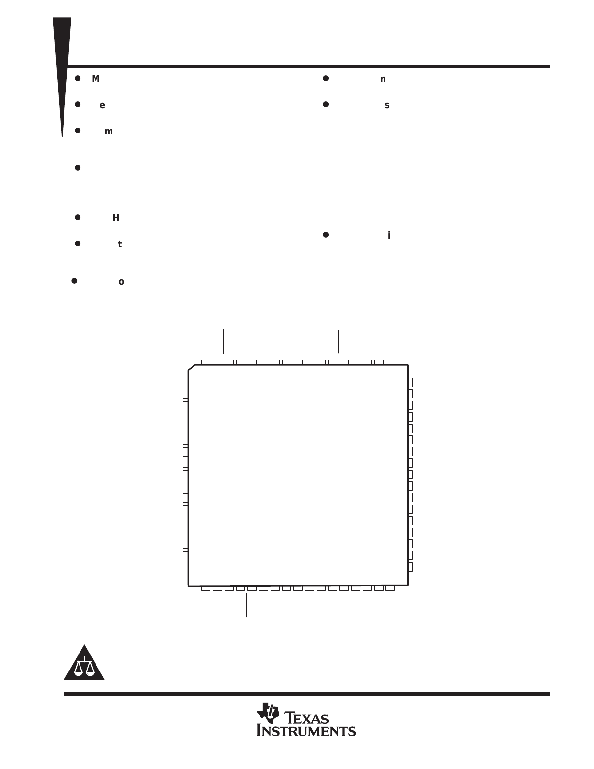
SN54ABTH18502A, SN54ABTH182502A . . . HV PACKAGE
SCAN TEST DEVICES
WITH 18-BIT UNIVERSAL BUS TRANSCEIVERS
SCBS164E – AUGUST 1993 – REVISED DECEMBER 1996
D
One Boundary-Scan Cell Per I/O
Architecture Improves Scan Efficiency
D
(TOP VIEW)
SCOPE
– IEEE Standard 1149.1-1990 Required
– Parallel-Signature Analysis at Inputs
– Pseudo-Random Pattern Generation
– Sample Inputs/Toggle Outputs
– Binary Count From Outputs
– Device Identification
– Even-Parity Opcodes
D
Packaged in 64-Pin Plastic Thin Quad Flat
(PM) Packages Using 0.5-mm
Center-to-Center Spacings and 68-Pin
Ceramic Quad Flat (HV) Packages Using
25-mil Center-to-Center Spacings
Instruction Set
Instructions and Optional CLAMP and
HIGHZ
From Outputs
1A2
1A1
1OEAB
GND
87 65493168672
1A3
1A4
1A5
GND
1A6
1A7
1A8
1A9
V
2A1
2A2
2A3
GND
2A4
2A5
2A6
10
11
12
13
14
15
16
17
18
NC
19
CC
20
21
22
23
24
25
26
28 29 30 31 32 33 34
2A9
2A7
2A8
GND
NC – No internal connection
1LEAB
1CLKAB
2LEAB
2OEAB
CC
VNCTMS
TDO
35 36 37 38 39
NC
TDI
2CLKAB
1CLKBA
1LEBA
1OEBA
66 652764 63 62 61
CC
V
TCK
2LEBA
2CLKBA
GND
1B1
1B2
40 41 42 43
2B9
GND
2OEBA
1B3
60
59
58
57
56
55
54
53
52
51
50
49
48
47
46
45
44
2B8
1B4
1B5
1B6
GND
1B7
1B8
1B9
V
CC
NC
2B1
2B2
2B3
2B4
GND
2B5
2B6
2B7
Please be aware that an important notice concerning availability, standard warranty, and use in critical applications of
Texas Instruments semiconductor products and disclaimers thereto appears at the end of this data sheet.
SCOPE, Widebus, UBT, and EPIC-ΙΙB are trademarks of Texas Instruments Incorporated.
UNLESS OTHERWISE NOTED this document contains PRODUCTION
DATA information current as of publication date. Products conform to
specifications per the terms of Texas Instruments standard warranty.
Production processing does not necessarily include testing of all
parameters.
POST OFFICE BOX 655303 • DALLAS, TEXAS 75265
Copyright 1996, Texas Instruments Incorporated
On products compliant to MIL-PRF-38535, all parameters are tested
unless otherwise noted. On all other products, production
processing does not necessarily include testing of all parameters.
1
SN54ABTH18502A, SN54ABTH182502A, SN74ABTH18502A, SN74ABTH182502A
SCAN TEST DEVICES
WITH 18-BIT UNIVERSAL BUS TRANSCEIVERS
SCBS164E – AUGUST 1993 – REVISED DECEMBER 1996
1A3
1A4
1A5
GND
1A6
1A7
1A8
1A9
V
CC
2A1
2A2
2A3
GND
2A4
2A5
2A6
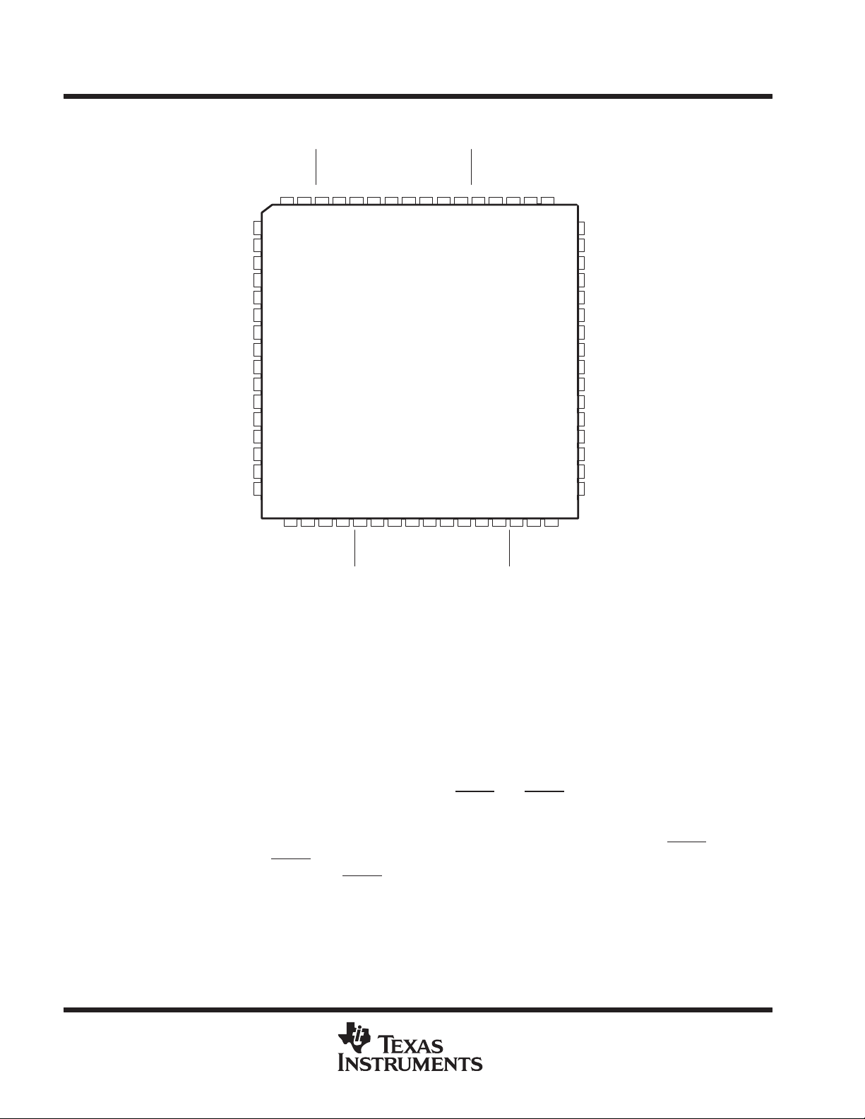
SN74ABTH18502A, SN74ABTH182502A . . . PM PACKAGE
1OEAB
1A1
GND
20
1A2
63 62 61 60 5964 58 56 55 5457
1
2
3
4
5
6
7
8
9
10
11
12
13
14
15
16
18 19
(TOP VIEW)
1CLKAB
TDO
1LEAB
21 22 23 24
CC
V
1LEBA
TMS
1CLKBA
53 521751 50 49
25 26 27 28 29
1OEBA
GND
30 31 32
1B1
1B2
1B3
48
47
46
45
44
43
42
41
40
39
38
37
36
35
34
33
1B4
1B5
1B6
GND
1B7
1B8
1B9
V
CC
2B1
2B2
2B3
2B4
GND
2B5
2B6
2B7
CC
2LEAB
2CLKAB
TDI
V
TCK
2CLKBA
GND
2LEBA
2B9
2OEBA
2B8
2A7
2A8
2A9
GND
2OEAB
description
The ’ABTH18502A and ’ABTH182502A scan test devices with 18-bit universal bus transceivers are members
of the Texas Instruments SCOPE testability integrated-circuit family. This family of devices supports IEEE
Standard 1 149.1-1990 boundary scan to facilitate testing of complex circuit-board assemblies. Scan access to
the test circuitry is accomplished via the 4-wire test access port (TAP) interface.
In the normal mode, these devices are 18-bit universal bus transceivers that combine D-type latches and D-type
flip-flops to allow data flow in transparent, latched, or clocked modes. They can be used either as two 9-bit
transceivers or one 18-bit transceiver. The test circuitry can be activated by the TAP to take snapshot samples
of the data appearing at the device pins or to perform a self test on the boundary-test cells. Activating the T AP
in the normal mode does not affect the functional operation of the SCOPE universal bus transceivers.
Data flow in each direction is controlled by output-enable (OEAB
and clock (CLKAB and CLKBA) inputs. For A-to-B data flow, the device operates in the transparent mode when
LEAB is high. When LEAB is low , the A-bus data is latched while CLKAB is held at a static low or high logic level.
Otherwise, if LEAB is low, A-bus data is stored on a low-to-high transition of CLKAB. When OEAB is low, the
B outputs are active. When OEAB
is high, the B outputs are in the high-impedance state. B-to-A data flow is
similar to A-to-B data flow but uses the OEBA, LEBA, and CLKBA inputs.
In the test mode, the normal operation of the SCOPE universal bus transceivers is inhibited and the test circuitry
is enabled to observe and control the I/O boundary of the device. When enabled, the test circuitry performs
boundary-scan test operations according to the protocol described in IEEE Standard 1149.1-1990.
and OEBA), latch-enable (LEAB and LEBA),
2
POST OFFICE BOX 655303 • DALLAS, TEXAS 75265
SN54ABTH18502A, SN54ABTH182502A, SN74ABTH18502A, SN74ABTH182502A
SCAN TEST DEVICES
WITH 18-BIT UNIVERSAL BUS TRANSCEIVERS
SCBS164E – AUGUST 1993 – REVISED DECEMBER 1996
description (continued)
Four dedicated test pins observe and control the operation of the test circuitry: test data input (TDI), test data
output (TDO), test mode select (TMS), and test clock (TCK). Additionally , the test circuitry performs other testing
functions such as parallel-signature analysis (PSA) on data inputs and pseudo-random pattern generation
(PRPG) from data outputs. All testing and scan operations are synchronized to the TAP interface.
Improved scan efficiency is accomplished through the adoption of a one boundary-scan cell (BSC) per I/O pin
architecture. This architecture is implemented in such a way as to capture the most pertinent test data. A
PSA/COUNT instruction also is included to ease the testing of memories and other circuits where a binary count
addressing scheme is useful.
Active bus-hold circuitry holds unused or floating data inputs at a valid logic level.
The B-port outputs of ’ABTH182502A, which are designed to source or sink up to 12 mA, include 25-Ω series
resistors to reduce overshoot and undershoot.
The SN54ABTH18502A and SN54ABTH182502A are characterized for operation over the full military
temperature range of –55°C to 125°C. The SN74ABTH18502A and SN74ABTH182502A are characterized for
operation from –40°C to 85°C.
FUNCTION TABLE
(normal mode, each register)
INPUTS
OEAB LEAB CLKAB A
L L L X B
L L ↑ LL
L L ↑ HH
L HXLL
L HXHH
H X X X Z
†
A-to-B data flow is shown. B-to-A data flow is similar
but uses OEBA
‡
Output level before the indicated steady-state input
conditions were established
, LEBA, and CLKBA.
†
OUTPUT
B
‡
0
POST OFFICE BOX 655303 • DALLAS, TEXAS 75265
3
SN54ABTH18502A, SN54ABTH182502A, SN74ABTH18502A, SN74ABTH182502A
SCAN TEST DEVICES
WITH 18-BIT UNIVERSAL BUS TRANSCEIVERS
SCBS164E – AUGUST 1993 – REVISED DECEMBER 1996
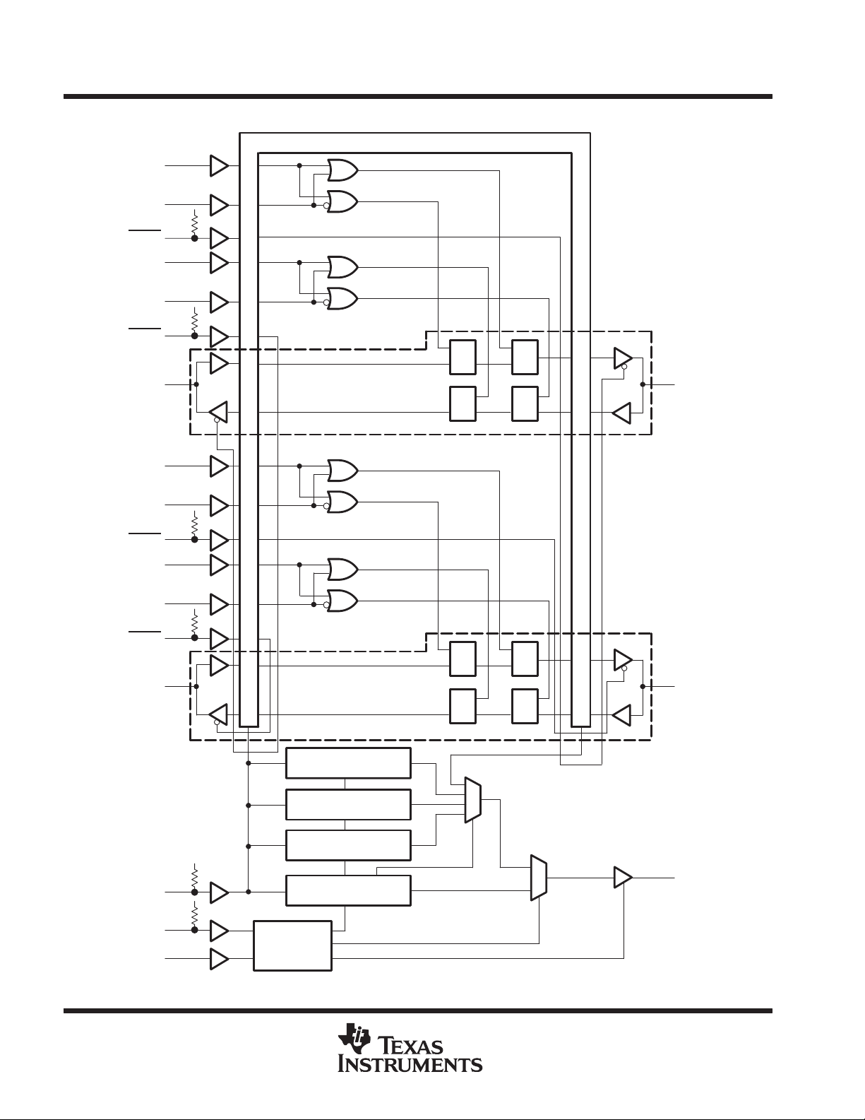
functional block diagram
1LEAB
1CLKAB
1OEAB
1LEBA
1CLKBA
1OEBA
1A1
2LEAB
2CLKAB
2OEAB
2LEBA
60
59
V
CC
62
54
55
V
CC
53
63
One of Nine Channels
22
23
V
CC
21
28
Boundary-Scan Register
C1
1D
C1
1D
C1
1D
C1
1D
51
1B1
2A1
TDI
TMS
TCK
27
V
CC
30
10
V
CC
24
V
CC
56
26
Controller
2CLKBA
2OEBA
Pin numbers shown are for the PM package.
One of Nine Channels
Bypass Register
Boundary-Control
Register
Identification
Register
Instruction
Register
TAP
C1
1D
C1
1D
C1
1D
C1
1D
40
58
2B1
TDO
4
POST OFFICE BOX 655303 • DALLAS, TEXAS 75265
SN54ABTH18502A, SN54ABTH182502A, SN74ABTH18502A, SN74ABTH182502A
WITH 18-BIT UNIVERSAL BUS TRANSCEIVERS
Terminal Functions
TERMINAL NAME DESCRIPTION
1A1–1A9,
2A1–2A9
1B1–1B9,
2B1–2B9
1CLKAB, 1CLKBA,
2CLKAB, 2CLKBA
GND Ground
1LEAB, 1LEBA,
2LEAB, 2LEBA
1OEAB, 1OEBA,
2OEAB
, 2OEBA
TCK
TDI
TDO
TMS
V
CC
Normal-function A-bus I/O ports. See function table for normal-mode logic.
Normal-function B-bus I/O ports. See function table for normal-mode logic.
Normal-function clock inputs. See function table for normal-mode logic.
Normal-function latch enables. See function table for normal-mode logic.
Normal-function output enables. See function table for normal-mode logic. An internal pullup at each terminal forces the
terminal to a high level if left unconnected.
T est clock. One of four terminals required by IEEE Standard 1149.1-1990. T est operations of the device are synchronous
to TCK. Data is captured on the rising edge of TCK and outputs change on the falling edge of TCK.
Test data input. One of four terminals required by IEEE Standard 1 149.1-1990. TDI is the serial input for shifting data
through the instruction register or selected data register. An internal pullup forces TDI to a high level if left unconnected.
T est data output. One of four terminals required by IEEE Standard 1 149.1-1990. TDO is the serial output for shifting data
through the instruction register or selected data register.
T est mode select. One of four terminals required by IEEE Standard 1149.1-1990. TMS directs the device through its T AP
controller states. An internal pullup forces TMS to a high level if left unconnected.
Supply voltage
SCAN TEST DEVICES
SCBS164E – AUGUST 1993 – REVISED DECEMBER 1996
POST OFFICE BOX 655303 • DALLAS, TEXAS 75265
5
SN54ABTH18502A, SN54ABTH182502A, SN74ABTH18502A, SN74ABTH182502A
SCAN TEST DEVICES
WITH 18-BIT UNIVERSAL BUS TRANSCEIVERS
SCBS164E – AUGUST 1993 – REVISED DECEMBER 1996
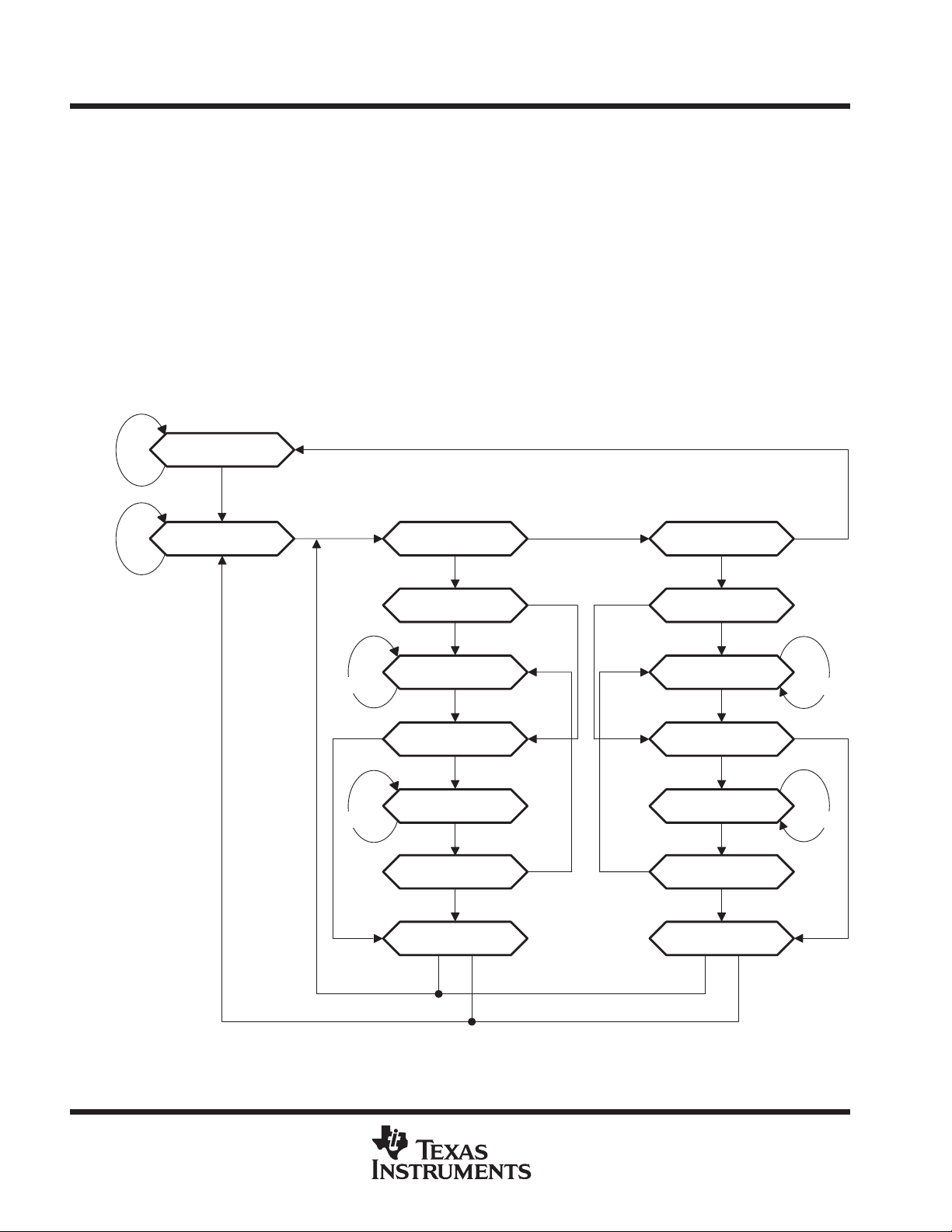
test architecture
Serial-test information is conveyed by means of a 4-wire test bus or TAP that conforms to IEEE Standard
1 149.1-1990. Test instructions, test data, and test control signals all are passed along this serial-test bus. The
TAP controller monitors two signals from the test bus, TCK and TMS. The TAP controller extracts the
synchronization (TCK) and state control (TMS) signals from the test bus and generates the appropriate on-chip
control signals for the test structures in the device. Figure 1 shows the TAP-controller state diagram.
The T AP controller is fully synchronous to the TCK signal. Input data is captured on the rising edge of TCK and
output data changes on the falling edge of TCK. This scheme ensures that data to be captured is valid for fully
one-half of the TCK cycle.
The functional block diagram illustrates the IEEE Standard 1149.1-1990 4-wire test bus and boundary-scan
architecture and the relationship among the test bus, the T AP controller, and the test registers. As illustrated,
the device contains an 8-bit instruction register and four test-data registers: a 48-bit boundary-scan register, a
3-bit boundary-control register, a 1-bit bypass register, and a 32-bit device-identification register.
Test-Logic-Reset
TMS = H
TMS = L
TMS = L
Run-Test/Idle Select-DR-Scan
TMS = L
Capture-DR
TMS = L
Shift-DR
TMS = L
TMS = H
TMS = H
Exit1-DR
TMS = L
Pause-DR
TMS = L
TMS = H
Exit2-DR
TMS = H
TMS = HTMS = H
TMS = H TMS = H
TMS = L
TMS = L
Select-IR-Scan
TMS = H
TMS = L
Capture-IR
TMS = L
Shift-IR
TMS = L
TMS = H
TMS = H
Exit1-IR
TMS = L
Pause-IR
TMS = L
TMS = H
Exit2-IR
TMS = H
Update-DR
TMS = LTMS = H
Update-IR
TMS = LTMS = H
Figure 1. TAP-Controller State Diagram
6
POST OFFICE BOX 655303 • DALLAS, TEXAS 75265

SN54ABTH18502A, SN54ABTH182502A, SN74ABTH18502A, SN74ABTH182502A
SCAN TEST DEVICES
WITH 18-BIT UNIVERSAL BUS TRANSCEIVERS
SCBS164E – AUGUST 1993 – REVISED DECEMBER 1996
state diagram description
The T AP controller is a synchronous finite state machine that provides test control signals throughout the device.
The state diagram shown in Figure 1 is in accordance with IEEE Standard 1149.1-1990. The TAP controller
proceeds through its states based on the level of TMS at the rising edge of TCK.
As shown, the T AP controller consists of 16 states. There are six stable states (indicated by a looping arrow in
the state diagram) and ten unstable states. A stable state is a state the T AP controller can retain for consecutive
TCK cycles. Any state that does not meet this criterion is an unstable state.
There are two main paths through the state diagram: one to access and control the selected data register and
one to access and control the instruction register. Only one register can be accessed at a time.
Test-Logic-Reset
The device powers up in the T est-Logic-Reset state. In the stable Test-Logic-Reset state, the test logic is reset
and is disabled so that the normal logic function of the device is performed. The instruction register is reset to
an opcode that selects the optional IDCODE instruction, if supported, or the BYP ASS instruction. Certain data
registers also can be reset to their power-up values.
The state machine is constructed such that the T AP controller returns to the Test-Logic-Reset state in no more
than five TCK cycles if TMS is left high. TMS has an internal pullup resistor that forces it high if left unconnected
or if a board defect causes it to be open circuited.
For the ’ABTH18502A and ’ABTH182502A, the instruction register is reset to the binary value 10000001, which
selects the IDCODE instruction. Bits 47–44 in the boundary-scan register are reset to logic 1, ensuring that
these cells, which control A-port and B-port outputs, are set to benign values (i.e., if test mode were invoked,
the outputs would be at high-impedance state). Reset values of other bits in the boundary-scan register should
be considered indeterminate. The boundary-control register is reset to the binary value 010, which selects the
PSA test operation.
Run-Test/Idle
The T AP controller must pass through the Run-T est/Idle state (from T est-Logic-Reset) before executing any test
operations. The Run-Test/Idle state also can be entered following data-register or instruction-register scans.
Run-Test/Idle is a stable state in which the test logic can be actively running a test or can be idle. The test
operations selected by the boundary-control register are performed while the TAP controller is in the
Run-Test/Idle state.
Select-DR-Scan, Select-lR-Scan
No specific function is performed in the Select-DR-Scan and Select-lR-Scan states, and the T AP controller exits
either of these states on the next TCK cycle. These states allow the selection of either data-register scan or
instruction-register scan.
Capture-DR
When a data-register scan is selected, the TAP controller must pass through the Capture-DR state. In the
Capture-DR state, the selected data register can capture a data value as specified by the current instruction.
Such capture operations occur on the rising edge of TCK, upon which the T AP controller exits the Capture-DR
state.
Shift-DR
Upon entry to the Shift-DR state, the data register is placed in the scan path between TDI and TDO, and on the
first falling edge of TCK, TDO goes from the high-impedance state to an active state. TDO enables to the logic
level present in the least-significant bit of the selected data register.
POST OFFICE BOX 655303 • DALLAS, TEXAS 75265
7

SN54ABTH18502A, SN54ABTH182502A, SN74ABTH18502A, SN74ABTH182502A
SCAN TEST DEVICES
WITH 18-BIT UNIVERSAL BUS TRANSCEIVERS
SCBS164E – AUGUST 1993 – REVISED DECEMBER 1996
Shift-DR (continued)
While in the stable Shift-DR state, data is serially shifted through the selected data register on each TCK cycle.
The first shift occurs on the first rising edge of TCK after entry to the Shift-DR state (i.e., no shifting occurs during
the TCK cycle in which the T AP controller changes from Capture-DR to Shift-DR or from Exit2-DR to Shift-DR).
The last shift occurs on the rising edge of TCK, upon which the TAP controller exits the Shift-DR state.
Exit1-DR, Exit2-DR
The Exit1-DR and Exit2-DR states are temporary states that end a data-register scan. It is possible to return
to the Shift-DR state from either Exit1-DR or Exit2-DR without recapturing the data register. On the first falling
edge of TCK after entry to Exit1-DR, TDO goes from the active state to the high-impedance state.
Pause-DR
No specific function is performed in the stable Pause-DR state, in which the TAP controller can remain
indefinitely . The Pause-DR state can suspend and resume data-register scan operations without loss of data.
Update-DR
If the current instruction calls for the selected data register to be updated with current data, such update occurs
on the falling edge of TCK, following entry to the Update-DR state.
Capture-IR
When an instruction-register scan is selected, the TAP controller must pass through the Capture-IR state. In
the Capture-IR state, the instruction register captures its current status value. This capture operation occurs
on the rising edge of TCK, upon which the T AP controller exits the Capture-IR state. For the ’ABTH18502A and
’ABTH182502A, the status value loaded in the Capture-IR state is the fixed binary value 10000001.
Shift-IR
Upon entry to the Shift-IR state, the instruction register is placed in the scan path between TDI and TDO, and
on the first falling edge of TCK, TDO goes from the high-impedance state to an active state. TDO enables to
the logic level present in the least-significant bit of the instruction register.
While in the stable Shift-IR state, instruction data is serially shifted through the instruction register on each TCK
cycle. The first shift occurs on the first rising edge of TCK after entry to the Shift-IR state (i.e., no shifting occurs
during the TCK cycle in which the TAP controller changes from Capture-IR to Shift-IR or from Exit2-IR to
Shift-IR). The last shift occurs on the rising edge of TCK, upon which the T AP controller exits the Shift-IR state.
Exit1-IR, Exit2-IR
The Exit1-IR and Exit2-IR states are temporary states that end an instruction-register scan. It is possible to
return to the Shift-IR state from either Exit1-IR or Exit2-IR without recapturing the instruction register. On the
first falling edge of TCK after entry to Exit1-IR, TDO goes from the active state to the high-impedance state.
Pause-IR
No specific function is performed in the stable Pause-IR state, in which the TAP controller can remain
indefinitely. The Pause-IR state can suspend and resume instruction-register scan operations without loss of
data.
Update-IR
The current instruction is updated and takes effect on the falling edge of TCK, following entry to the Update-IR
state.
8
POST OFFICE BOX 655303 • DALLAS, TEXAS 75265
SN54ABTH18502A, SN54ABTH182502A, SN74ABTH18502A, SN74ABTH182502A
SCAN TEST DEVICES
WITH 18-BIT UNIVERSAL BUS TRANSCEIVERS
SCBS164E – AUGUST 1993 – REVISED DECEMBER 1996
register overview
With the exception of the bypass and device-identification registers, any test register can be thought of as a
serial-shift register with a shadow latch on each bit. The bypass and device-identification registers differ in that
they contain only a shift register. During the appropriate capture state (Capture-IR for instruction register,
Capture-DR for data registers), the shift register can be parallel loaded from a source specified by the current
instruction. During the appropriate shift state (Shift-IR or Shift-DR), the contents of the shift register are shifted
out from TDO while new contents are shifted in at TDI. During the appropriate update state (Update-IR or
Update-DR), the shadow latches are updated from the shift register.
instruction register description
The instruction register (IR) is eight bits long and tells the device what instruction is to be executed. Information
contained in the instruction includes the mode of operation (either normal mode, in which the device performs
its normal logic function, or test mode, in which the normal logic function is inhibited or altered), the test operation
to be performed, which of the four data registers is to be selected for inclusion in the scan path during
data-register scans, and the source of data to be captured into the selected data register during Capture-DR.
Table 3 lists the instructions supported by the ’ABTH18502A and ’ABTH182502A. The even-parity feature
specified for SCOPE devices is supported in this device. Bit 7 of the instruction opcode is the parity bit. Any
instructions that are defined for SCOPE devices but are not supported by this device default to BYPASS.
During Capture-IR, the IR captures the binary value 10000001. As an instruction is shifted in, this value is shifted
out via TDO and can be inspected as verification that the IR is in the scan path. During Update-IR, the value
that has been shifted into the IR is loaded into shadow latches. At this time, the current instruction is updated
and any specified mode change takes effect. At power up or in the Test-Logic-Reset state, the IR is reset to the
binary value 10000001, which selects the IDCODE instruction. The IR order of scan is shown in Figure 2.
Bit 7
Parity
(MSB)
Bit 6 Bit 5 Bit 4 Bit 3 Bit 2 Bit 1
Bit 0
(LSB)
TDOTDI
Figure 2. Instruction Register Order of Scan
POST OFFICE BOX 655303 • DALLAS, TEXAS 75265
9
SN54ABTH18502A, SN54ABTH182502A, SN74ABTH18502A, SN74ABTH182502A
SCAN TEST DEVICES
WITH 18-BIT UNIVERSAL BUS TRANSCEIVERS
SCBS164E – AUGUST 1993 – REVISED DECEMBER 1996
data register description
boundary-scan register
The boundary-scan register (BSR) is 48 bits long. It contains one boundary-scan cell (BSC) for each
normal-function input pin and one BSC for each normal-function I/O pin (one single cell for both input data and
output data). The BSR is used to store test data that is to be applied externally to the device output pins, and/or
to capture data that appears internally at the outputs of the normal on-chip logic and/or externally at the device
input pins.
The source of data to be captured into the BSR during Capture-DR is determined by the current instruction. The
contents of the BSR can change during Run-Test/Idle as determined by the current instruction. At power up or
in T est-Logic-Reset, BSCs 47–44 are reset to logic 1, ensuring that these cells, which control A-port and B-port
outputs, are set to benign values (i.e., if test mode were invoked, the outputs would be at high-impedance state).
Reset values of other BSCs should be considered indeterminate.
The BSR order of scan is from TDI through bits 47–0 to TDO. T able 1 shows the BSR bits and their associated
device pin signals.
Table 1. Boundary-Scan Register Configuration
BSR BIT
NUMBER
47 2OEAB 35 2A9-I/O 17 2B9-I/O
46 1OEAB 34 2A8-I/O 16 2B8-I/O
45 2OEBA 33 2A7-I/O 15 2B7-I/O
44 1OEBA 32 2A6-I/O 14 2B6-I/O
43 2CLKAB 31 2A5-I/O 13 2B5-I/O
42 1CLKAB 30 2A4-I/O 12 2B4-I/O
41 2CLKBA 29 2A3-I/O 11 2B3-I/O
40 1CLKBA 28 2A2-I/O 10 2B2-I/O
39 2LEAB 27 2A1-I/O 9 2B1-I/O
38 1LEAB 26 1A9-I/O 8 1B9-I/O
37 2LEBA 25 1A8-I/O 7 1B8-I/O
36 1LEBA 24 1A7-I/O 6 1B7-I/O
23 1A6-I/O 5 1B6-I/O
22 1A5-I/O 4 1B5-I/O
21 1A4-I/O 3 1B4-I/O
20 1A3-I/O 2 1B3-I/O
19 1A2-I/O 1 1B2-I/O
18 1A1-I/O 0 1B1-I/O
DEVICE
SIGNAL
BSR BIT
NUMBER
DEVICE
SIGNAL
BSR BIT
NUMBER
DEVICE
SIGNAL
10
POST OFFICE BOX 655303 • DALLAS, TEXAS 75265
SN54ABTH18502A, SN54ABTH182502A, SN74ABTH18502A, SN74ABTH182502A
SCAN TEST DEVICES
WITH 18-BIT UNIVERSAL BUS TRANSCEIVERS
SCBS164E – AUGUST 1993 – REVISED DECEMBER 1996
boundary-control register
The boundary-control register (BCR) is three bits long. The BCR is used in the context of the boundary-run test
(RUNT) instruction to implement additional test operations not included in the basic SCOPE instruction set.
Such operations include PRPG, PSA, and binary count up (COUNT). Table 4 shows the test operations that
are decoded by the BCR.
During Capture-DR, the contents of the BCR are not changed. At power up or in Test-Logic-Reset, the BCR is
reset to the binary value 010, which selects the PSA test operation. The BCR order of scan is shown in
Figure 3.
Bit 2
(MSB)
Bit 1
Bit 0
(LSB)
TDOTDI
Figure 3. Boundary-Control Register Order of Scan
bypass register
The bypass register is a 1-bit scan path that can be selected to shorten the length of the system scan path,
reducing the number of bits per test pattern that must be applied to complete a test operation. During
Capture-DR, the bypass register captures a logic 0. The bypass register order of scan is shown in
Figure 4.
Bit 0
TDOTDI
Figure 4. Bypass Register Order of Scan
POST OFFICE BOX 655303 • DALLAS, TEXAS 75265
11
SN54ABTH18502A, SN54ABTH182502A, SN74ABTH18502A, SN74ABTH182502A
SCAN TEST DEVICES
WITH 18-BIT UNIVERSAL BUS TRANSCEIVERS
SCBS164E – AUGUST 1993 – REVISED DECEMBER 1996
device-identification register
The device-identification register (IDR) is 32 bits long. It can be selected and read to identify the manufacturer,
part number, and version of this device.
For the ’ABTH18502A , the binary value 000000000000001001 1100000010111 1 (0002702F, hex) is captured
(during Capture-DR state) in the IDR to identify this device as Texas Instruments SN54/74ABTH18502A.
For the ’ABTH182502A , the binary value 0000000000000010101 10000001011 1 1 (0002B02F , hex) is captured
(during Capture-DR state) in the IDR to identify this device as Texas Instruments SN54/74ABTH182502A.
The IDR order of scan is from TDI through bits 31–0 to TDO. T able 2 shows the IDR bits and their significance.
Table 2. Device-Identification Register Configuration
IDR BIT
NUMBER
31 VERSION3 27 PARTNUMBER15 11 MANUFACTURER10
30 VERSION2 26 PARTNUMBER14 10 MANUFACTURER09
29 VERSION1 25 PARTNUMBER13 9 MANUFACTURER08
28 VERSION0 24 PARTNUMBER12 8 MANUFACTURER07
23 PARTNUMBER11 7 MANUFACTURER06
22 PARTNUMBER10 6 MANUFACTURER05
21 PARTNUMBER09 5 MANUFACTURER04
20 PARTNUMBER08 4 MANUFACTURER03
19 PARTNUMBER07 3 MANUFACTURER02
18 PARTNUMBER06 2 MANUFACTURER01
17 PARTNUMBER05 1 MANUFACTURER00
16 PARTNUMBER04 0 LOGIC1
15 PARTNUMBER03
14 PARTNUMBER02
13 PARTNUMBER01
12 PARTNUMBER00
†
Note that for TI products, bits 11–0 of the device-identification register always contain the binary value 000000101111
(02F, hex).
IDENTIFICATION
SIGNIFICANCE
IDR BIT
NUMBER
IDENTIFICATION
SIGNIFICANCE
IDR BIT
NUMBER
IDENTIFICATION
SIGNIFICANCE
†
†
†
†
†
†
†
†
†
†
†
†
12
POST OFFICE BOX 655303 • DALLAS, TEXAS 75265

SN54ABTH18502A, SN54ABTH182502A, SN74ABTH18502A, SN74ABTH182502A
SCAN TEST DEVICES
WITH 18-BIT UNIVERSAL BUS TRANSCEIVERS
SCBS164E – AUGUST 1993 – REVISED DECEMBER 1996
instruction-register opcode description
The instruction-register opcodes are shown in Table 3. The following descriptions detail the operation of each
instruction.
Table 3. Instruction-Register Opcodes
BINARY CODE
BIT 7 → BIT 0
MSB → LSB
00000000 EXTEST Boundary scan Boundary scan Test
10000001 IDCODE Identification read Device identification Normal
10000010 SAMPLE/PRELOAD Sample boundary Boundary scan Normal
0000001 1 BYPASS
10000100 BYPASS
00000101 BYPASS
00000110 HIGHZ Control boundary to high impedance Bypass Modified test
100001 11 CLAMP Control boundary to 1/0 Bypass Test
10001000 BYPASS
00001001 RUNT Boundary-run test Bypass Test
00001010 READBN Boundary read Boundary scan Normal
1000101 1 READBT Boundary read Boundary scan T est
00001 100 CELLTST Boundary self test Boundary scan Normal
10001 101 TOPHIP Boundary toggle outputs Bypass Test
10001 110 SCANCN Boundary-control register scan Boundary control Normal
00001 11 1 SCANCT Boundary-control register scan Boundary control Test
All others BYPASS Bypass scan Bypass Normal
†
Bit 7 is used to maintain even parity in the 8-bit instruction.
‡
The BYPASS instruction is executed in lieu of a SCOPE instruction that is not supported in the ’ABTH18502A or ’ABTH182502A.
†
SCOPE OPCODE DESCRIPTION
‡
‡
‡
‡
SELECTED DATA
REGISTER
Bypass scan Bypass Normal
Bypass scan Bypass Normal
Bypass scan Bypass Normal
Bypass scan Bypass Normal
MODE
boundary scan
This instruction conforms to the IEEE Standard 1149.1-1990 EXTEST instruction. The BSR is selected in the
scan path. Data appearing at the device input and I/O pins is captured in the associated BSCs. Data that has
been scanned into the I/O BSCs for pins in the output mode is applied to the device I/O pins. Data present at
the device pins, except for output-enables, is passed through the BSCs to the normal on-chip logic. For I/O pins,
the operation of a pin as input or output is determined by the contents of the output-enable BSCs (bits 47–44
of the BSR). When a given output enable is active (logic 0), the associated I/O pins operate in the output mode.
Otherwise, the I/O pins operate in the input mode. The device operates in the test mode.
identification read
This instruction conforms to the IEEE Standard 1149.1-1990 IDCODE instruction. The IDR is selected in the
scan path. The device operates in the normal mode.
sample boundary
This instruction conforms to the IEEE Standard 1149.1-1990 SAMPLE/PRELOAD instruction. The BSR is
selected in the scan path. Data appearing at the device input pins and I/O pins in the input mode is captured
in the associated BSCs, while data appearing at the outputs of the normal on-chip logic is captured in the BSCs
associated with I/O pins in the output mode. The device operates in the normal mode.
POST OFFICE BOX 655303 • DALLAS, TEXAS 75265
13

SN54ABTH18502A, SN54ABTH182502A, SN74ABTH18502A, SN74ABTH182502A
SCAN TEST DEVICES
WITH 18-BIT UNIVERSAL BUS TRANSCEIVERS
SCBS164E – AUGUST 1993 – REVISED DECEMBER 1996
bypass scan
This instruction conforms to the IEEE Standard 1149.1-1990 BYPASS instruction. The bypass register is
selected in the scan path. A logic 0 value is captured in the bypass register during Capture-DR. The device
operates in the normal mode.
control boundary to high impedance
This instruction conforms to the IEEE Standard 1149.1a-1993 HIGHZ instruction. The bypass register is
selected in the scan path. A logic 0 value is captured in the bypass register during Capture-DR. The device
operates in a modified test mode in which all device I/O pins are placed in the high-impedance state, the device
input pins remain operational, and the normal on-chip logic function is performed.
control boundary to 1/0
This instruction conforms to the IEEE Standard 1149.1a-1993 CLAMP instruction. The bypass register is
selected in the scan path. A logic 0 value is captured in the bypass register during Capture-DR. Data in the I/O
BSCs for pins in the output mode is applied to the device I/O pins. The device operates in the test mode.
boundary-run test
The bypass register is selected in the scan path. A logic 0 value is captured in the bypass register during
Capture-DR. The device operates in the test mode. The test operation specified in the BCR is executed during
Run-Test/Idle. The five test operations decoded by the BCR are: sample inputs/toggle outputs (TOPSIP),
PRPG, PSA, simultaneous PSA and PRPG (PSA/PRPG), and simultaneous PSA and binary count up
(PSA/COUNT).
boundary read
The BSR is selected in the scan path. The value in the BSR remains unchanged during Capture-DR. This
instruction is useful for inspecting data after a PSA operation.
boundary self test
The BSR is selected in the scan path. All BSCs capture the inverse of their current values during Capture-DR.
In this way , the contents of the shadow latches can be read out to verify the integrity of both shift-register and
shadow-latch elements of the BSR. The device operates in the normal mode.
boundary toggle outputs
The bypass register is selected in the scan path. A logic 0 value is captured in the bypass register during
Capture-DR. Data in the shift-register elements of the selected output-mode BSCs is toggled on each rising
edge of TCK in Run-T est/Idle, updated in the shadow latches, and applied to the associated device I/O pins on
each falling edge of TCK in Run-Test/Idle. Data in the input-mode BSCs remains constant. Data appearing at
the device input or I/O pins is not captured in the input-mode BSCs. The device operates in the test mode.
boundary-control-register scan
The BCR is selected in the scan path. The value in the BCR remains unchanged during Capture-DR. This
operation must be performed before a RUNT operation to specify which test operation is to be executed.
14
POST OFFICE BOX 655303 • DALLAS, TEXAS 75265

SN54ABTH18502A, SN54ABTH182502A, SN74ABTH18502A, SN74ABTH182502A
SCAN TEST DEVICES
WITH 18-BIT UNIVERSAL BUS TRANSCEIVERS
SCBS164E – AUGUST 1993 – REVISED DECEMBER 1996
boundary-control-register opcode description
The BCR opcodes are decoded from BCR bits 2–0 as shown in T able 4. The selected test operation is performed
while the RUNT instruction is executed in the Run-T est/Idle state. The following descriptions detail the operation
of each BCR instruction and illustrate the associated PSA and PRPG algorithms.
Table 4. Boundary-Control Register Opcodes
BINARY CODE
BIT 2 → BIT 0
MSB → LSB
X00 Sample inputs/toggle outputs (TOPSIP)
X01 Pseudo-random pattern generation/36-bit mode (PRPG)
X10 Parallel-signature analysis/36-bit mode (PSA)
011 Simultaneous PSA and PRPG/18-bit mode (PSA/PRPG)
111 Simultaneous PSA and binary count up/18-bit mode (PSA/COUNT)
While the control input BSCs (bits 47–36) are not included in the toggle, PSA, PRPG, or COUNT algorithms,
the output-enable BSCs (bits 47–44 of the BSR) control the drive state (active or high impedance) of the selected
device output pins. These BCR instructions are valid only when both bytes of the device are operating in one
direction of data flow (that is, 1OEAB ≠ 1OEBA and 2OEAB ≠ 2OEBA) and in the same direction of data flow
(that is, 1OEAB = 2OEAB and 1OEBA = 2OEBA). Otherwise, the bypass instruction is operated.
DESCRIPTION
sample inputs/toggle outputs (TOPSIP)
Data appearing at the selected device input-mode I/O pins is captured in the shift-register elements of the
associated BSCs on each rising edge of TCK. Data in the shift-register elements of the selected output-mode
BSCs is toggled on each rising edge of TCK, updated in the shadow latches, and applied to the associated
device I/O pins on each falling edge of TCK.
POST OFFICE BOX 655303 • DALLAS, TEXAS 75265
15

SN54ABTH18502A, SN54ABTH182502A, SN74ABTH18502A, SN74ABTH182502A
SCAN TEST DEVICES
WITH 18-BIT UNIVERSAL BUS TRANSCEIVERS
SCBS164E – AUGUST 1993 – REVISED DECEMBER 1996
pseudo-random pattern generation (PRPG)
A pseudo-random pattern is generated in the shift-register elements of the selected BSCs on each rising edge
of TCK, updated in the shadow latches, and applied to the associated device output-mode I/O pins on each
falling edge of TCK. Figures 5 and 6 illustrate the 36-bit linear-feedback shift-register algorithms through which
the patterns are generated. An initial seed value should be scanned into the BSR before performing this
operation. A seed value of all zeroes does not produce additional patterns.
2A7-I/O 2A6-I/O 2A5-I/O 2A4-I/O 2A3-I/O 2A2-I/O 2A1-I/O2A8-I/O2A9-I/O
1A7-I/O 1A6-I/O 1A5-I/O 1A4-I/O 1A3-I/O 1A2-I/O 1A1-I/O1A8-I/O1A9-I/O
2B8-I/O 2B7-I/O 2B6-I/O 2B5-I/O 2B4-I/O 2B3-I/O 2B2-I/O 2B1-I/O2B9-I/O
=
1B8-I/O 1B7-I/O 1B6-I/O 1B5-I/O 1B4-I/O 1B3-I/O 1B2-I/O 1B1-I/O1B9-I/O
Figure 5. 36-Bit PRPG Configuration (1OEAB = 2OEAB = 0, 1OEBA = 2OEBA = 1)
16
POST OFFICE BOX 655303 • DALLAS, TEXAS 75265
SN54ABTH18502A, SN54ABTH182502A, SN74ABTH18502A, SN74ABTH182502A
WITH 18-BIT UNIVERSAL BUS TRANSCEIVERS
pseudo-random pattern generation (PRPG) (continued)
2B7-I/O 2B6-I/O 2B5-I/O 2B4-I/O 2B3-I/O 2B2-I/O 2B1-I/O2B8-I/O2B9-I/O
1B7-I/O 1B6-I/O 1B5-I/O 1B4-I/O 1B3-I/O 1B2-I/O 1B1-I/O1B8-I/O1B9-I/O
2A8-I/O 2A7-I/O 2A6-I/O 2A5-I/O 2A4-I/O 2A3-I/O 2A2-I/O 2A1-I/O2A9-I/O
SCAN TEST DEVICES
SCBS164E – AUGUST 1993 – REVISED DECEMBER 1996
=
1A8-I/O 1A7-I/O 1A6-I/O 1A5-I/O 1A4-I/O 1A3-I/O 1A2-I/O 1A1-I/O1A9-I/O
Figure 6. 36-Bit PRPG Configuration (1OEAB = 2OEAB = 1, 1OEBA = 2OEBA = 0)
POST OFFICE BOX 655303 • DALLAS, TEXAS 75265
17
SN54ABTH18502A, SN54ABTH182502A, SN74ABTH18502A, SN74ABTH182502A
SCAN TEST DEVICES
WITH 18-BIT UNIVERSAL BUS TRANSCEIVERS
SCBS164E – AUGUST 1993 – REVISED DECEMBER 1996
parallel-signature analysis (PSA)
Data appearing at the selected device input-mode I/O pins is compressed into a 36-bit parallel signature in the
shift-register elements of the selected BSCs on each rising edge of TCK. Data in the shadow latches of the
selected output-mode BSCs remains constant and is applied to the associated device I/O pins. Figures 7 and 8
illustrate the 36-bit linear-feedback shift-register algorithms through which the signature is generated. An initial
seed value should be scanned into the BSR before performing this operation.
2A7-I/O 2A6-I/O 2A5-I/O 2A4-I/O 2A3-I/O 2A2-I/O 2A1-I/O2A8-I/O2A9-I/O
1A7-I/O 1A6-I/O 1A5-I/O 1A4-I/O 1A3-I/O 1A2-I/O 1A1-I/O1A8-I/O1A9-I/O
2B8-I/O 2B7-I/O 2B6-I/O 2B5-I/O 2B4-I/O 2B3-I/O 2B2-I/O 2B1-I/O2B9-I/O
=
=
1B8-I/O 1B7-I/O 1B6-I/O 1B5-I/O 1B4-I/O 1B3-I/O 1B2-I/O 1B1-I/O1B9-I/O
Figure 7. 36-Bit PSA Configuration (1OEAB = 2OEAB = 0, 1OEBA = 2OEBA = 1)
18
POST OFFICE BOX 655303 • DALLAS, TEXAS 75265

SN54ABTH18502A, SN54ABTH182502A, SN74ABTH18502A, SN74ABTH182502A
parallel-signature analysis (PSA) (continued)
2B7-I/O 2B6-I/O 2B5-I/O 2B4-I/O 2B3-I/O 2B2-I/O 2B1-I/O2B8-I/O2B9-I/O
1B7-I/O 1B6-I/O 1B5-I/O 1B4-I/O 1B3-I/O 1B2-I/O 1B1-I/O1B8-I/O1B9-I/O
2A8-I/O 2A7-I/O 2A6-I/O 2A5-I/O 2A4-I/O 2A3-I/O 2A2-I/O 2A1-I/O2A9-I/O
SCAN TEST DEVICES
WITH 18-BIT UNIVERSAL BUS TRANSCEIVERS
SCBS164E – AUGUST 1993 – REVISED DECEMBER 1996
=
=
1A8-I/O 1A7-I/O 1A6-I/O 1A5-I/O 1A4-I/O 1A3-I/O 1A2-I/O 1A1-I/O1A9-I/O
Figure 8. 36-Bit PSA Configuration (1OEAB = 2OEAB = 1, 1OEBA = 2OEBA = 0)
POST OFFICE BOX 655303 • DALLAS, TEXAS 75265
19

SN54ABTH18502A, SN54ABTH182502A, SN74ABTH18502A, SN74ABTH182502A
SCAN TEST DEVICES
WITH 18-BIT UNIVERSAL BUS TRANSCEIVERS
SCBS164E – AUGUST 1993 – REVISED DECEMBER 1996
simultaneous PSA and PRPG (PSA/PRPG)
Data appearing at the selected device input-mode I/O pins is compressed into an 18-bit parallel signature in
the shift-register elements of the selected input-mode BSCs on each rising edge of TCK. At the same time, an
18-bit pseudo-random pattern is generated in the shift-register elements of the selected output-mode BSCs on
each rising edge of TCK, updated in the shadow latches, and applied to the associated device I/O pins on each
falling edge of TCK. Figures 9 and 10 illustrate the 18-bit linear-feedback shift-register algorithms through which
the signature and patterns are generated. An initial seed value should be scanned into the BSR before
performing this operation. A seed value of all zeroes does not produce additional patterns.
2A7-I/O 2A6-I/O 2A5-I/O 2A4-I/O 2A3-I/O 2A2-I/O 2A1-I/O2A8-I/O2A9-I/O
1A7-I/O 1A6-I/O 1A5-I/O 1A4-I/O 1A3-I/O 1A2-I/O 1A1-I/O1A8-I/O1A9-I/O
2B8-I/O 2B7-I/O 2B6-I/O 2B5-I/O 2B4-I/O 2B3-I/O 2B2-I/O 2B1-I/O2B9-I/O
=
=
1B8-I/O 1B7-I/O 1B6-I/O 1B5-I/O 1B4-I/O 1B3-I/O 1B2-I/O 1B1-I/O1B9-I/O
Figure 9. 18-Bit PSA/PRPG Configuration (1OEAB = 2OEAB = 0, 1OEBA = 2OEBA = 1)
20
POST OFFICE BOX 655303 • DALLAS, TEXAS 75265

SN54ABTH18502A, SN54ABTH182502A, SN74ABTH18502A, SN74ABTH182502A
WITH 18-BIT UNIVERSAL BUS TRANSCEIVERS
simultaneous PSA and PRPG (PSA/PRPG) (continued)
2B7-I/O 2B6-I/O 2B5-I/O 2B4-I/O 2B3-I/O 2B2-I/O 2B1-I/O2B8-I/O2B9-I/O
1B7-I/O 1B6-I/O 1B5-I/O 1B4-I/O 1B3-I/O 1B2-I/O 1B1-I/O1B8-I/O1B9-I/O
SCAN TEST DEVICES
SCBS164E – AUGUST 1993 – REVISED DECEMBER 1996
2A8-I/O 2A7-I/O 2A6-I/O 2A5-I/O 2A4-I/O 2A3-I/O 2A2-I/O 2A1-I/O2A9-I/O
=
=
1A8-I/O 1A7-I/O 1A6-I/O 1A5-I/O 1A4-I/O 1A3-I/O 1A2-I/O 1A1-I/O1A9-I/O
Figure 10. 18-Bit PSA/PRPG Configuration (1OEAB = 2OEAB = 1, 1OEBA = 2OEBA = 0)
POST OFFICE BOX 655303 • DALLAS, TEXAS 75265
21

SN54ABTH18502A, SN54ABTH182502A, SN74ABTH18502A, SN74ABTH182502A
SCAN TEST DEVICES
WITH 18-BIT UNIVERSAL BUS TRANSCEIVERS
SCBS164E – AUGUST 1993 – REVISED DECEMBER 1996
simultaneous PSA and binary count up (PSA/COUNT)
Data appearing at the selected device input-mode I/O pins is compressed into an 18-bit parallel signature in
the shift-register elements of the selected input-mode BSCs on each rising edge of TCK. At the same time, an
18-bit binary count-up pattern is generated in the shift-register elements of the selected output-mode BSCs on
each rising edge of TCK, updated in the shadow latches, and applied to the associated device I/O pins on each
falling edge of TCK. Figures 11 and 12 illustrate the 18-bit linear-feedback shift-register algorithms through
which the signature is generated. An initial seed value should be scanned into the BSR before performing this
operation.
2A7-I/O 2A6-I/O 2A5-I/O 2A4-I/O 2A3-I/O 2A2-I/O 2A1-I/O2A8-I/O2A9-I/O
1A7-I/O 1A6-I/O 1A5-I/O 1A4-I/O 1A3-I/O 1A2-I/O 1A1-I/O1A8-I/O1A9-I/O
MSB
2B8-I/O 2B7-I/O 2B6-I/O 2B5-I/O 2B4-I/O 2B3-I/O 2B2-I/O 2B1-I/O2B9-I/O
LSB
=
=
1B8-I/O 1B7-I/O 1B6-I/O 1B5-I/O 1B4-I/O 1B3-I/O 1B2-I/O 1B1-I/O1B9-I/O
Figure 11. 18-Bit PSA/COUNT Configuration (1OEAB = 2OEAB = 0, 1OEBA = 2OEBA = 1)
22
POST OFFICE BOX 655303 • DALLAS, TEXAS 75265

SN54ABTH18502A, SN54ABTH182502A, SN74ABTH18502A, SN74ABTH182502A
WITH 18-BIT UNIVERSAL BUS TRANSCEIVERS
simultaneous PSA and binary count up (PSA/COUNT) (continued)
2B7-I/O 2B6-I/O 2B5-I/O 2B4-I/O 2B3-I/O 2B2-I/O 2B1-I/O2B8-I/O2B9-I/O
SCAN TEST DEVICES
SCBS164E – AUGUST 1993 – REVISED DECEMBER 1996
1B9-I/O
MSB
2A8-I/O 2A7-I/O 2A6-I/O 2A5-I/O 2A4-I/O 2A3-I/O 2A2-I/O 2A1-I/O2A9-I/O
=
=
1A8-I/O 1A7-I/O 1A6-I/O 1A5-I/O 1A4-I/O 1A3-I/O 1A2-I/O 1A1-I/O1A9-I/O
1B7-I/O 1B6-I/O 1B5-I/O 1B4-I/O 1B3-I/O 1B2-I/O 1B1-I/O1B8-I/O
LSB
Figure 12. 18-Bit PSA/COUNT Configuration (1OEAB = 2OEAB = 1, 1OEBA = 2OEBA = 0)
POST OFFICE BOX 655303 • DALLAS, TEXAS 75265
23

SN54ABTH18502A, SN54ABTH182502A, SN74ABTH18502A, SN74ABTH182502A
SCAN TEST DEVICES
WITH 18-BIT UNIVERSAL BUS TRANSCEIVERS
SCBS164E – AUGUST 1993 – REVISED DECEMBER 1996
timing description
All test operations of the ’ABTH18502A and ’ABTH182502A are synchronous to TCK. Data on the TDI, TMS,
and normal-function inputs is captured on the rising edge of TCK. Data appears on the TDO and normal-function
output pins on the falling edge of TCK. The T AP controller is advanced through its states (as shown in Figure 1)
by changing the value of TMS on the falling edge of TCK and then applying a rising edge to TCK.
A simple timing example is shown in Figure 13. In this example, the TAP controller begins in the
Test-Logic-Reset state and is advanced through its states, to perform one instruction-register scan and one
data-register scan. While in the Shift-IR and Shift-DR states, TDI is used to input serial data, and TDO is used
to output serial data. The TAP controller is then returned to the Test-Logic-Reset state. Table 5 details the
operation of the test circuitry during each TCK cycle.
Table 5. Explanation of Timing Example
TCK
CYCLE(S)
1 Test-Logic-Reset
2 Run-Test/Idle
3 Select-DR-Scan
4 Select-IR-Scan
5 Capture-IR
6 Shift-IR
7–13 Shift-IR
14 Exit1-IR TDO becomes inactive (goes to the high-impedance state) on the falling edge of TCK.
15 Update-IR The IR is updated with the new instruction (BYPASS) on the falling edge of TCK.
16 Select-DR-Scan
17 Capture-DR
18 Shift-DR
19–20 Shift-DR The binary value 101 is shifted in via TDI, while the binary value 010 is shifted out via TDO.
21 Exit1-DR TDO becomes inactive (goes to the high-impedance state) on the falling edge of TCK.
22 Update-DR In general, the selected data register is updated with the new data on the falling edge of TCK.
23 Select-DR-Scan
24 Select-IR-Scan
25 Test-Logic-Reset Test operation completed
TAP STATE
AFTER TCK
DESCRIPTION
TMS is changed to a logic 0 value on the falling edge of TCK to begin advancing the TAP controller toward
the desired state.
The IR captures the 8-bit binary value 10000001 on the rising edge of TCK as the TAP controller exits the
Capture-IR state.
TDO becomes active and TDI is made valid on the falling edge of TCK. The first bit is shifted into the TAP on
the rising edge of TCK as the TAP controller advances to the next state.
One bit is shifted into the IR on each TCK rising edge. With TDI held at a logic 1 value, the 8-bit binary value
11111111 is serially scanned into the IR. At the same time, the 8-bit binary value 10000001 is serially scanned
out of the IR via TDO. In TCK cycle 13, TMS is changed to a logic 1 value to end the IR scan on the next TCK
cycle. The last bit of the instruction is shifted as the TAP controller advances from Shift-IR to Exit1-IR.
The bypass register captures a logic 0 value on the rising edge of TCK as the TAP controller exits the
Capture-DR state.
TDO becomes active and TDI is made valid on the falling edge of TCK. The first bit is shifted into the TAP on
the rising edge of TCK as the TAP controller advances to the next state.
24
POST OFFICE BOX 655303 • DALLAS, TEXAS 75265

ООООО
ООООО
SN54ABTH18502A, SN54ABTH182502A, SN74ABTH18502A, SN74ABTH182502A
timing description (continued)
1 2 3 4 5 6 7 8 9 10 11 12 13 14 15 16 17 18 19 20 21 22 23 24 25
TCK
TMS
TDI
TDO
SCAN TEST DEVICES
WITH 18-BIT UNIVERSAL BUS TRANSCEIVERS
SCBS164E – AUGUST 1993 – REVISED DECEMBER 1996
TAP
Controller
State
Run-Test/Idle
Test-Logic-Reset
Select-DR-Scan
Capture-IR
Select-IR-Scan
Shift-IR
3-State (TDO) or Don’t Care (TDI)
Exit1-IR
Update-IR
Capture-DR
Select-DR-Scan
Shift-DR
Exit1-DR
Update-DR
Select-IR-Scan
Select-DR-Scan
Figure 13. Timing Example
absolute maximum ratings over operating free-air temperature range (unless otherwise noted)
Supply voltage range, VCC –0.5 V to 7 V. . . . . . . . . . . . . . . . . . . . . . . . . . . . . . . . . . . . . . . . . . . . . . . . . . . . . . . . . .
Input voltage range, VI: except I/O ports (see Note 1) –0.5 V to 7 V. . . . . . . . . . . . . . . . . . . . . . . . . . . . . . . . . .
I/O ports (see Note 1) –0.5 V to 5.5 V. . . . . . . . . . . . . . . . . . . . . . . . . . . . . . . . . . . . . . . .
Voltage range applied to any output in the high state or power-off state, VO –0.5 V to 5.5 V. . . . . . . . . . . . . .
Current into any output in the low state, IO: SN54ABTH18502A 96 mA. . . . . . . . . . . . . . . . . . . . . . . . . . . . . . . .
SN54ABTH182502A (A port or TDO) 96 mA. . . . . . . . . . . . . . . . .
SN54ABTH182502A (B port) 30 mA. . . . . . . . . . . . . . . . . . . . . . . .
SN74ABTH18502A 128 mA. . . . . . . . . . . . . . . . . . . . . . . . . . . . . . .
SN74ABTH182502A (A port or TDO) 128 mA. . . . . . . . . . . . . . . .
SN74ABTH182502A (B port) 30 mA. . . . . . . . . . . . . . . . . . . . . . . .
Input clamp current, I
Output clamp current, I
Continuous current through VCC 576 mA. . . . . . . . . . . . . . . . . . . . . . . . . . . . . . . . . . . . . . . . . . . . . . . . . . . . . . . . . .
Continuous current through GND 1152 mA. . . . . . . . . . . . . . . . . . . . . . . . . . . . . . . . . . . . . . . . . . . . . . . . . . . . . . . .
Maximum power dissipation at T
Storage temperature range, T
†
Stresses beyond those listed under “absolute maximum ratings” may cause permanent damage to the device. These are stress ratings only, and
functional operation of the device at these or any other conditions beyond those indicated under “recommended operating conditions” is not
implied. Exposure to absolute-maximum-rated conditions for extended periods may affect device reliability.
NOTES: 1. The input and output negative-voltage ratings can be exceeded if the input and output clamp-current ratings are observed.
2. The maximum package power dissipation is calculated using a junction temperature of 150°C and a board trace length of 75 mils.
For more information, refer to the
Book
, literature number SCBD002.
(V
< 0) –18 mA. . . . . . . . . . . . . . . . . . . . . . . . . . . . . . . . . . . . . . . . . . . . . . . . . . . . . . . . . . .
IK
I
(V
< 0) –50 mA. . . . . . . . . . . . . . . . . . . . . . . . . . . . . . . . . . . . . . . . . . . . . . . . . . . . . . . .
OK
O
= 55°C (in still air) (see Note 2): PM package 1 W. . . . . . . . . . . . . . . . . . . .
A
–65°C to 150°C. . . . . . . . . . . . . . . . . . . . . . . . . . . . . . . . . . . . . . . . . . . . . . . . . . .
stg
Package Thermal Considerations
application note in the
ABT Advanced BiCMOS T echnology Data
Test-Logic-Reset
†
POST OFFICE BOX 655303 • DALLAS, TEXAS 75265
25
SN54ABTH18502A, SN54ABTH182502A, SN74ABTH18502A, SN74ABTH182502A
UNIT
SCAN TEST DEVICES
WITH 18-BIT UNIVERSAL BUS TRANSCEIVERS
SCBS164E – AUGUST 1993 – REVISED DECEMBER 1996
recommended operating conditions
SN54ABTH18502A SN74ABTH18502A
MIN MAX MIN MAX
V
CC
V
IH
V
IL
V
I
I
OH
I
OL
∆t/∆v Input transition rise or fall rate 10 10 ns/V
T
A
Supply voltage 4.5 5.5 4.5 5.5 V
High-level input voltage 2 2 V
Low-level input voltage 0.8 0.8 V
Input voltage 0 V
High-level output current –24 –32 mA
Low-level output current 48 64 mA
Operating free-air temperature –55 125 –40 85 °C
CC
0 V
CC
V
26
POST OFFICE BOX 655303 • DALLAS, TEXAS 75265

I
µ
I
‡
A or B ports
V
4.5 V
A
,
V
CC
5.5 V,
SN54ABTH18502A, SN54ABTH182502A, SN74ABTH18502A, SN74ABTH182502A
SCAN TEST DEVICES
WITH 18-BIT UNIVERSAL BUS TRANSCEIVERS
SCBS164E – AUGUST 1993 – REVISED DECEMBER 1996
electrical characteristics over recommended operating free-air temperature range (unless
otherwise noted)
SN54ABTH18502A
PARAMETER TEST CONDITIONS
V
IK
V
OH
V
OL
CLK, LE, TCK
I
I
I
IH
I
IL
I(hold)
I
OZH
I
OZL
I
OZPU
I
OZPD
I
off
I
CEX
§
I
O
I
CC
∆I
CC
C
i
C
io
C
o
†
All typical values are at VCC = 5 V.
‡
The parameter I
§
Not more than one output should be tested at a time, and the duration of the test should not exceed one second.
¶
This is the increase in supply current for each input that is at the specified TTL voltage level rather than VCC or GND.
VCC = 0 to 5.5 V,
A or B ports VCC = 5.5 V, VI = VCC or GND ±20 ±20
OE, TDI, TMS VCC = 5.5 V, VI = V
OE, TDI, TMS VCC = 5.5 V, VI = GND –40 –150 –40 –150 µA
p
TDO
TDO
TDO
TDO
Outputs high VCC = 5.5 V, VO = 5.5 V 50 50 µA
Outputs high
Outputs low
Outputs disabled
¶
Control inputs VI = 2.5 V or 0.5 V 7 pF
A or B ports VO = 2.5 V or 0.5 V 10 pF
TDO VO = 2.5 V or 0.5 V 7 pF
includes the off-state output leakage current.
I(hold)
VCC = 4.5 V, II = –18 mA –1.2 –1.2 V
VCC = 4.5 V, IOH = –3 mA 2.5 2.5
VCC = 5 V, IOH = –3 mA 3 3
VCC = 4.5 V, IOH = –24 mA 2 2
VCC = 4.5 V, IOL = 48 mA 0.55 0.55 V
VCC = 0 to 5.5 V, VI = VCC or GND ±1 ±1
CC
=
CC
VCC = 2.1 V to 5.5 V,
VO = 2.7 V, OE
VCC = 2.1 V to 5.5 V,
VO = 0.5 V, OE
VCC = 0 to 2.1 V,
VO = 2.7 V or 0.5 V, OE
VCC = 2.1 V to 0,
VO = 2.7 V or 0.5 V, OE
VCC = 0, VI or VO ≤ 4.5 V ±100 µA
VCC = 5.5 V, VO = 2.5 V –50 –110 –200 –50 –200 mA
V
= 5.5 V
IO = 0,
VI = VCC or GND
VCC = 5.5 V, One input at 3.4 V,
Other inputs at VCC or GND
VI = 0.8 V 75 220 500 75 500
VI = 2 V –75 –180 –500 –75 –500
= 2 V
= 2 V
= 0.8 V
= 0.8 V
A or B ports
TA = 25°C TA = –55°C to 125°C
MIN
†
TYP
MAX MIN MAX
10 10 µA
10 10 µA
–10 –10 µA
±50 ±50 µA
±50 ±50 µA
1.6 5.5 5.5
19 24 24
0.9 3.6 3.6
1.5 1.5 mA
UNIT
V
µA
µ
mA
POST OFFICE BOX 655303 • DALLAS, TEXAS 75265
27

SN54ABTH18502A, SN54ABTH182502A, SN74ABTH18502A, SN74ABTH182502A
V
V
V
V
VOLV
V
V
I
A
I
‡
A or B ports
V
V
A
V
CC
SCAN TEST DEVICES
WITH 18-BIT UNIVERSAL BUS TRANSCEIVERS
SCBS164E – AUGUST 1993 – REVISED DECEMBER 1996
electrical characteristics over recommended operating free-air temperature range (unless
otherwise noted)
SN74ABTH18502A
PARAMETER TEST CONDITIONS
V
IK
OH
I
I
IH
I
IL
I(hold)
I
OZH
I
OZL
I
OZPU
I
OZPD
I
off
I
CEX
I
O
I
CC
∆I
CC
C
i
C
io
C
o
†
All typical values are at VCC = 5 V.
‡
The parameter I
§
Not more than one output should be tested at a time, and the duration of the test should not exceed one second.
¶
This is the increase in supply current for each input that is at the specified TTL voltage level rather than VCC or GND.
CLK, LE, TCK VCC = 0 to 5.5 V, VI = VCC or GND ±1 ±1
A or B ports VCC = 5.5 V, VI = VCC or GND ±20 ±20
OE, TDI, TMS VCC = 5.5 V, VI = V
OE, TDI, TMS VCC = 5.5 V, VI = GND –40 –150 –40 –150 µA
p
TDO
TDO
TDO
TDO
Outputs high VCC = 5.5 V, VO = 5.5 V 50 50 µA
§
Outputs high
Outputs low
Outputs disabled
¶
Control inputs VI = 2.5 V or 0.5 V 5 pF
A or B ports VO = 2.5 V or 0.5 V 10 pF
TDO VO = 2.5 V or 0.5 V 8 pF
includes the off-state output leakage current.
I(hold)
VCC = 4.5 V, II = –18 mA –1.2 –1.2 V
VCC = 4.5 V, IOH = –3 mA 2.5 2.5
VCC = 5 V, IOH = –3 mA 3 3
= 4.5
CC
= 4.5
CC
= 4.5
CC
VCC = 2.1 V to 5.5 V,
VO = 2.7 V, OE
VCC = 2.1 V to 5.5 V,
VO = 0.5 V, OE
VCC = 0 to 2.1 V,
VO = 2.7 V or 0.5 V, OE
VCC = 2.1 V to 0,
VO = 2.7 V or 0.5 V, OE
VCC = 0, VI or VO ≤ 4.5 V ±100 ±100 µA
VCC = 5.5 V, VO = 2.5 V –50 –110 –200 –50 –200 mA
=
= 5.5 V,
IO = 0,
VI = VCC or GND
VCC = 5.5 V, One input at 3.4 V,
Other inputs at VCC or GND
IOH = –24 mA 2
IOH = –32 mA 2 2
IOL = 48 mA 0.55
IOL = 64 mA 0.55 0.55
CC
VI = 0.8 V 75 220 500 75 500
VI = 2 V –75 –180 –500 –75 –500
= 2 V
= 2 V
= 0.8 V
= 0.8 V
A or B ports
TA = 25°C TA = –40°C to 85°C
MIN TYP†MAX MIN MAX
10 10 µA
10 10 µA
–10 –10 µA
±50 ±50 µA
±50 ±50 µA
1.6 2.2 2.2
19 24 24
0.9 2 2
1.5 1.5 mA
UNIT
µ
µ
mA
28
POST OFFICE BOX 655303 • DALLAS, TEXAS 75265

UNIT
twPulse duration
ns
A bef
LEAB↓
LEBA↓
thHold time
ns
UNIT
SN54ABTH18502A, SN54ABTH182502A, SN74ABTH18502A, SN74ABTH182502A
SCAN TEST DEVICES
WITH 18-BIT UNIVERSAL BUS TRANSCEIVERS
SCBS164E – AUGUST 1993 – REVISED DECEMBER 1996
timing requirements over recommended ranges of supply voltage and operating free-air
temperature (unless otherwise noted) (normal mode) (see Figure 14)1
SN54ABTH18502A SN74ABTH18502A
MIN MAX MIN MAX
f
clock
t
su
timing requirements over recommended ranges of supply voltage and operating free-air
temperature (unless otherwise noted) (test mode) (see Figure 14)
f
clock
t
w
t
su
t
h
t
d
t
r
* On products compliant to MIL-PRF-38535, this parameter is not production tested.
Clock frequency CLKAB or CLKBA 0 100 0 100 MHz
CLKAB or CLKBA high or low 3.8 3.5
LEAB or LEBA high 3.5 3.5
A before CLKAB↑ or B before CLKBA↑ 3.5 3.5
Setup time
Clock frequency TCK 0 50 0 50 MHz
Pulse duration TCK high or low 8 8 ns
Setup time
Hold time
Delay time Power up to TCK↑ 50* 50 ns
Rise time VCC power up 1* 1 µs
ore
A after CLKAB↑ or B after CLKBA↑ 2.9 0.5
A after LEAB↓ or B after LEBA↓ 4.0 3
A, B, CLK, LE, or OE before TCK↑ 6 6
TDI before TCK↑
TMS before TCK↑ 3 3
A, B, CLK, LE, or OE after TCK↑ 2.9 1.5
TDI after TCK↑
TMS after TCK↑ 1.5 1.5
or B before
CLK high 4.0 3.5
CLK low 2 2
SN54ABTH18502A SN74ABTH18502A
MIN MAX MIN MAX
4.5 4.5
1 1
ns
ns
ns
POST OFFICE BOX 655303 • DALLAS, TEXAS 75265
29

SN54ABTH18502A, SN54ABTH182502A, SN74ABTH18502A, SN74ABTH182502A
A or B
B or A
ns
CLKAB or CLKBA
B or A
ns
LEAB or LEBA
B or A
ns
OEAB
OEBA
B or A
ns
OEAB or OEBA
B or A
ns
A or B
B or A
ns
CLKAB or CLKBA
B or A
ns
LEAB or LEBA
B or A
ns
OEAB
OEBA
B or A
ns
OEAB or OEBA
B or A
ns
SCAN TEST DEVICES
WITH 18-BIT UNIVERSAL BUS TRANSCEIVERS
SCBS164E – AUGUST 1993 – REVISED DECEMBER 1996
switching characteristics over recommended ranges of supply voltage and operating free-air
temperature (unless otherwise noted) (normal mode) (see Figure 14)1
SN54ABTH18502A
PARAMETER
f
max
t
PLH
t
PHL
t
PLH
t
PHL
t
PLH
t
PHL
t
PZH
t
PZL
t
PHZ
t
PLZ
FROM
(INPUT)
CLKAB or CLKBA 100 130 100 MHz
or
TO
(OUTPUT)
VCC = 5 V,
TA = 25°C
MIN TYP MAX MIN MAX
1.5 3.1 5 1.5 6
1.5 3.6 5 1.5 6
1.5 3.7 5.2 1.5 6.4
1.5 3.8 5.2 1.5 6.4
1.5 3.9 5.5 1.5 6.5
1.5 3.6 5.5 1.5 6.5
1.5 4 5.8 1.5 7.5
1.5 4.2 5.8 1.5 7.5
2.8 5.9 7.2 2.8 8.9
2 4.5 6 2 7.5
VCC = 4.5 V to 5.5 V,
TA = –55°C to 125°C
UNIT
switching characteristics over recommended ranges of supply voltage and operating free-air
temperature (unless otherwise noted) (normal mode) (see Figure 14)
SN74ABTH18502A
PARAMETER
f
max
t
PLH
t
PHL
t
PLH
t
PHL
t
PLH
t
PHL
t
PZH
t
PZL
t
PHZ
t
PLZ
FROM
(INPUT)
CLKAB or CLKBA 100 130 100 MHz
or
TO
(OUTPUT)
VCC = 5 V,
TA = 25°C
MIN TYP MAX MIN MAX
1.5 3.1 5 1.5 5.5
1.5 3.6 5 1.5 5.5
1.5 3.7 5 1.5 5.5
1.5 3.8 5 1.5 5.5
1.5 3.9 5.5 1.5 6
1.5 3.6 5.5 1.5 6
1.5 4 5.8 1.5 7
1.5 4.2 5.8 1.5 7
3 5.9 7 3 8
2 4.5 6 2 7
VCC = 4.5 V to 5.5 V,
TA = –40°C to 85°C
UNIT
30
POST OFFICE BOX 655303 • DALLAS, TEXAS 75265

(INPUT)
(OUTPUT)
TCK↓
A or B
ns
TCK↓
TDO
ns
TCK↓
A or B
ns
TCK↓
TDO
ns
TCK↓
A or B
ns
TCK↓
TDO
ns
SN54ABTH18502A, SN54ABTH182502A, SN74ABTH18502A, SN74ABTH182502A
SCAN TEST DEVICES
WITH 18-BIT UNIVERSAL BUS TRANSCEIVERS
SCBS164E – AUGUST 1993 – REVISED DECEMBER 1996
switching characteristics over recommended ranges of supply voltage and operating free-air
temperature (unless otherwise noted) (test mode) (see Figure 14)
PARAMETER
f
max
t
PLH
t
PHL
t
PLH
t
PHL
t
PZH
t
PZL
t
PZH
t
PZL
t
PHZ
t
PLZ
t
PHZ
t
PLZ
FROM
TCK 50 90 50 50 MHz
TO
VCC = 5 V,
TA = 25°C
MIN TYP MAX MIN MAX MIN MAX
2.5 7.4 11 2.5 14.5 2.5 13.1
2.5 7.6 10.8 2.5 14 2.5 12.4
2 3.8 5.1 2 7 2 5.6
2 4 5.1 2 7 2 5.6
4 8 11.5 4 14.5 4 13.4
4 8 11.8 4 15 4 13.6
2 3.9 5.7 2 7.5 2 6.6
2 4.2 6.2 2 8 2 6.9
4 10.8 13 4 18 4 15
3 9.1 13.3 3 17.5 3 15
3 5.3 6.8 3 8 3 7.2
2.5 4.2 5.5 2.5 8 2.5 6.3
SN54ABTH18502A SN74ABTH18502A
UNIT
POST OFFICE BOX 655303 • DALLAS, TEXAS 75265
31

SN54ABTH18502A, SN54ABTH182502A, SN74ABTH18502A, SN74ABTH182502A
UNIT
IOHHigh-level output current
mA
IOLLow-level output current
mA
SCAN TEST DEVICES
WITH 18-BIT UNIVERSAL BUS TRANSCEIVERS
SCBS164E – AUGUST 1993 – REVISED DECEMBER 1996
recommended operating conditions
SN54ABTH182502A SN74ABTH182502A
MIN MAX MIN MAX
V
CC
V
IH
V
IL
V
I
∆t/∆v Input transition rise or fall rate 10 10 ns/V
T
A
Supply voltage 4.5 5.5 4.5 5.5 V
High-level input voltage 2 2 V
Low-level input voltage 0.8 0.8 V
Input voltage 0 V
p
p
Operating free-air temperature –55 125 –40 85 °C
A port, TDO –24 –32
B port –12 –12
A port, TDO 48 64
B port 12 12
CC
0 V
CC
V
PRODUCT PREVIEW information concerns products in the formative or
design phase of development. Characteristic data and other
specifications are design goals. Texas Instruments reserves the right to
change or discontinue these products without notice.
32
POST OFFICE BOX 655303 • DALLAS, TEXAS 75265

PARAMETER
TEST CONDITIONS
UNIT
A port, TDO
V
4.5 V
V
V
B port
V
V
A port, TDO
V
4.5 V
V
V
B port
V
V
I
A
I
‡
A or B ports
V
V
A
I
§
mA
V
CC
I
CC
A or B orts
mA
SN54ABTH18502A, SN54ABTH182502A, SN74ABTH18502A, SN74ABTH182502A
SCAN TEST DEVICES
WITH 18-BIT UNIVERSAL BUS TRANSCEIVERS
SCBS164E – AUGUST 1993 – REVISED DECEMBER 1996
electrical characteristics over recommended operating free-air temperature range (unless
otherwise noted)
TA = 25°C SN54ABTH182502A SN74ABTH182502A
MIN TYP†MAX MIN MAX MIN MAX
V
IK
p
OH
p
p
OL
p
CLK, LE, TCK
I
A or B ports
I
IH
I
IL
I(hold)
I
OZH
I
OZL
I
OZPU
I
OZPD
I
off
I
CEX
O
∆I
CC
* On products compliant to MIL-PRF-38535, this parameter does not apply.
†
All typical values are at VCC = 5 V.
‡
The parameter I
§
Not more than one output should be tested at a time, and the duration of the test should not exceed one second.
¶
This is the increase in supply current for each input that is at the specified TTL voltage level rather than VCC or GND.
OE, TDI, TMS VCC = 5.5 V, VI = V
OE, TDI, TMS VCC = 5.5 V, VI = GND –40 –150 –40 –150 –40 –150 µA
p
TDO
TDO
TDO
TDO
Outputs high VCC = 5.5 V, VO = 5.5 V 50 50 50 µA
A port, TDO VCC = 5.5 V, VO = 2.5 V –50 –110 –200 –50 –200 –50 –200
B port VCC = 5.5 V, VO = 2.5 V –25 –55 –100 –25 –100 –25 –100
Outputs high
Outputs low
Outputs
disabled
¶
I(hold)
VCC = 4.5 V, II = –18 mA –1.2 –1.2 –1.2 V
VCC = 4.5 V, IOH = –3 mA 2.5 2.5 2.5
VCC = 5 V, IOH = –3 mA 3 3 3
=
CC
VCC = 4.5 V, IOH = –1 mA 3.35 3.3 3.35
VCC = 5 V, IOH = –1 mA 3.85 3.8 3.85
= 4.5
CC
=
CC
= 4.5
CC
VCC = 0 to 5.5 V,
VI = VCC or GND
VCC = 5.5 V,
VI = VCC or GND
= 4.5
CC
VCC = 2.1 V to 5.5 V,
VO = 2.7 V, OE
VCC = 2.1 V to 5.5 V,
VO = 0.5 V, OE
VCC = 0 to 2.1 V,
VO = 2.7 V or 0.5 V, OE
VCC = 2.1 V to 0,
VO = 2.7 V or 0.5 V, OE
VCC = 0, VI or VO ≤ 4.5 V ±100 ±100 µA
=
= 5.5 V,
IO = 0,
VI = VCC or
GND
VCC = 5.5 V, One input at 3.4 V,
Other inputs at VCC or GND
includes the off-state output leakage current.
IOH = –24 mA 2 2
IOH = –32 mA 2* 2
IOH = –3 mA 3.1 3 3.1
IOH = –12 mA 2.6* 2.6
IOL = 48 mA 0.55 0.55
IOL = 64 mA 0.55* 0.55
IOL = 8 mA 0.8 0.8 0.65
IOL = 12 mA 0.8* 0.8
±1 ±1 ±1
±20 ±20 ±20
CC
VI = 0.8 V 75 220 500 75 500
VI = 2 V –75 –180 –500 –75 –500
= 2 V
= 2 V
= 0.8 V
= 0.8 V
1.6 2.2 2.2 2.2
p
0.9 2 2 2
10 10 10 µA
10 10 10 µA
–10 –10 –10 µA
±50 ±50 µA
±50 ±50 µA
21 27 27 27
1.5 1.5 1.5 mA
µ
µ
PRODUCT PREVIEW information concerns products in the formative or
design phase of development. Characteristic data and other
specifications are design goals. Texas Instruments reserves the right to
change or discontinue these products without notice.
POST OFFICE BOX 655303 • DALLAS, TEXAS 75265
33

SN54ABTH18502A, SN54ABTH182502A, SN74ABTH18502A, SN74ABTH182502A
PARAMETER
TEST CONDITIONS
UNIT
UNIT
twPulse duration
ns
A bef
LEAB↓
LEBA↓
thHold time
ns
UNIT
SCAN TEST DEVICES
WITH 18-BIT UNIVERSAL BUS TRANSCEIVERS
SCBS164E – AUGUST 1993 – REVISED DECEMBER 1996
electrical characteristics over recommended operating free-air temperature range (unless
otherwise noted) (continued)
TA = 25°C SN54ABTH182502A SN74ABTH182502A
MIN TYP†MAX MIN MAX MIN MAX
C
i
C
io
C
o
†
All typical values are at VCC = 5 V.
timing requirements over recommended ranges of supply voltage and operating free-air
temperature (unless otherwise noted) (normal mode) (see Figure 14)12
f
clock
t
su
Control
inputs
A or B ports VO = 2.5 V or 0.5 V 10 pF
TDO VO = 2.5 V or 0.5 V 8 pF
Clock frequency CLKAB or CLKBA 0 100 0 100 MHz
Setup time
VI = 2.5 V or 0.5 V 5 pF
SN54ABTH182502A SN74ABTH182502A
MIN MAX MIN MAX
CLKAB or CLKBA high or low 3.5 3.5
LEAB or LEBA high 3.5 3.5
A before CLKAB↑ or B before CLKBA↑ 3.5 3.5
ore
A after CLKAB↑ or B after CLKBA↑ 0.5 0.5
A after LEAB↓ or B after LEBA↓ 3 3
or B before
CLK high 3.5 3.5
CLK low 2 2
ns
timing requirements over recommended ranges of supply voltage and operating free-air
temperature (unless otherwise noted) (test mode) (see Figure 14)
SN54ABTH182502A SN74ABTH182502A
MIN MAX MIN MAX
f
clock
t
w
t
su
t
h
t
d
t
r
Clock frequency TCK 0 50 0 50 MHz
Pulse duration TCK high or low 8 8 ns
A, B, CLK, LE, or OE before TCK↑ 6 6
Setup time
Hold time
Delay time Power up to TCK↑ 50 50 ns
Rise time VCC power up 1 1 µs
TDI before TCK↑
TMS before TCK↑ 3 3
A, B, CLK, LE, or OE after TCK↑ 1.5 1.5
TDI after TCK↑
TMS after TCK↑ 1.5 1.5
4.5 4.5
1 1
ns
ns
PRODUCT PREVIEW information concerns products in the formative or
design phase of development. Characteristic data and other
specifications are design goals. Texas Instruments reserves the right to
change or discontinue these products without notice.
34
POST OFFICE BOX 655303 • DALLAS, TEXAS 75265

(INPUT)
(OUTPUT)
A
B
ns
B
A
ns
CLKAB
B
ns
CLKBA
A
ns
LEAB
B
ns
LEBA
A
ns
OEAB
OEBA
B or A
ns
OEAB or OEBA
B or A
ns
(INPUT)
(OUTPUT)
TCK↓
A or B
ns
TCK↓
TDO
ns
TCK↓
A or B
ns
TCK↓
TDO
ns
TCK↓
A or B
ns
TCK↓
TDO
ns
SN54ABTH18502A, SN54ABTH182502A, SN74ABTH18502A, SN74ABTH182502A
SCAN TEST DEVICES
WITH 18-BIT UNIVERSAL BUS TRANSCEIVERS
SCBS164E – AUGUST 1993 – REVISED DECEMBER 1996
switching characteristics over recommended ranges of supply voltage and operating free-air
temperature (unless otherwise noted) (normal mode) (see Figure 14)12
PARAMETER
f
max
t
PLH
t
PHL
t
PLH
t
PHL
t
PLH
t
PHL
t
PLH
t
PHL
t
PLH
t
PHL
t
PLH
t
PHL
t
PZH
t
PZL
t
PHZ
t
PLZ
FROM
CLKAB or
CLKBA
or
TO
VCC = 5 V,
TA = 25°C
MIN TYP MAX MIN MAX MIN MAX
100 130 100 100 MHz
1.5 3.1 5 1.5 6 1.5 5.5
1.5 3.6 5.6 1.5 6.4 1.5 6.2
1.5 3.1 5 1.5 6 1.5 5.5
1.5 3.6 5 1.5 6 1.5 5.5
1.5 3.7 5.4 1.5 6.2 1.5 6.1
1.5 4 5.8 1.5 6.4 1.5 6.2
1.5 3.7 5 1.5 6 1.5 5.5
1.5 3.8 5 1.5 6 1.5 5.5
1.5 3.9 5.6 1.5 6.5 1.5 6.3
1.5 3.6 5.6 1.5 6.5 1.5 6.2
1.5 3.9 5.5 1.5 6.5 1.5 6
1.5 3.6 5.5 1.5 6.5 1.5 6
1.5 4 5.8 1.5 7.5 1.5 7
1.5 4.2 5.8 1.5 7.5 1.5 7
3 5.9 7 3 8.5 3 8
2 4.5 6 2 7.5 2 7
SN54ABTH182502A SN74ABTH182502A
UNIT
switching characteristics over recommended ranges of supply voltage and operating free-air
temperature (unless otherwise noted) (test mode) (see Figure 14)
PARAMETER
f
max
t
PLH
t
PHL
t
PLH
t
PHL
t
PZH
t
PZL
t
PZH
t
PZL
t
PHZ
t
PLZ
t
PHZ
t
PLZ
FROM
TCK 50 90 50 50 MHz
TO
VCC = 5 V,
TA = 25°C
MIN TYP MAX MIN MAX MIN MAX
2.5 7.4 11 2.5 14.5 2.5 13.1
2.5 7.6 10.8 2.5 14 2.5 12.4
2 3.8 5.1 2 7 2 5.6
2 4 5.1 2 7 2 5.6
4 8 11.5 4 14.5 4 13.4
4 8 11.8 4 15 4 13.6
2 3.9 5.7 2 7.5 2 6.6
2 4.2 6.2 2 8 2 6.9
4 10.8 13 4 18 4 15
3 9.1 13.3 3 17.5 3 15
3 5.3 6.8 3 8 3 7.2
2.5 4.2 5.5 2.5 8 2.5 6.3
SN54ABTH182502A SN74ABTH182502A
UNIT
PRODUCT PREVIEW information concerns products in the formative or
design phase of development. Characteristic data and other
specifications are design goals. Texas Instruments reserves the right to
change or discontinue these products without notice.
POST OFFICE BOX 655303 • DALLAS, TEXAS 75265
35

SN54ABTH18502A, SN54ABTH182502A, SN74ABTH18502A, SN74ABTH182502A
SCAN TEST DEVICES
WITH 18-BIT UNIVERSAL BUS TRANSCEIVERS
SCBS164E – AUGUST 1993 – REVISED DECEMBER 1996
PARAMETER MEASUREMENT INFORMATION
7 V
From Output
Under Test
CL = 50 pF
(see Note A)
Input
500 Ω
500 Ω
LOAD CIRCUIT
t
w
1.5 V 1.5 V
VOLTAGE WAVEFORMS
PULSE DURATION
S1
Open
GND
3 V
0 V
Timing Input
Data Input
TEST S1
t
PLH/tPHL
t
PLZ/tPZL
t
PHZ/tPZH
t
su
1.5 V 1.5 V
VOLTAGE WAVEFORMS
SETUP AND HOLD TIMES
Open
Open
1.5 V
t
7 V
h
3 V
0 V
3 V
0 V
Input
t
PLH
Output
t
PHL
Output
PROPAGATION DELAY TIMES
INVERTING AND NONINVERTING OUTPUTS
NOTES: A. CL includes probe and jig capacitance.
B. Waveform 1 is for an output with internal conditions such that the output is low except when disabled by the output control.
Waveform 2 is for an output with internal conditions such that the output is high except when disabled by the output control.
C. All input pulses are supplied by generators having the following characteristics: PRR ≤ 10 MHz, ZO = 50 Ω, tr ≤ 2.5 ns , tf≤ 2.5 ns.
D. The outputs are measured one at a time with one transition per measurement.
1.5 V 1.5 V
1.5 V
VOLTAGE WAVEFORMS
Figure 14. Load Circuit and Voltage Waveforms
t
PHL
1.5 V
t
PLH
1.5 V1.5 V
3 V
0 V
V
V
V
V
OH
OL
OH
OL
Output
Control
Output
Waveform 1
S1 at 7 V
(see Note B)
Output
Waveform 2
S1 at Open
(see Note B)
1.5 V
t
PZL
t
PLZ
1.5 V
t
t
PZH
ENABLE AND DISABLE TIMES
LOW- AND HIGH-LEVEL ENABLING
PHZ
1.5 V
VOLTAGE WAVEFORMS
1.5 V
VOL + 0.3 V
VOH – 0.3 V
3 V
0 V
3.5 V
V
OL
V
OH
[
0 V
36
POST OFFICE BOX 655303 • DALLAS, TEXAS 75265

IMPORTANT NOTICE
T exas Instruments and its subsidiaries (TI) reserve the right to make changes to their products or to discontinue
any product or service without notice, and advise customers to obtain the latest version of relevant information
to verify, before placing orders, that information being relied on is current and complete. All products are sold
subject to the terms and conditions of sale supplied at the time of order acknowledgement, including those
pertaining to warranty, patent infringement, and limitation of liability.
TI warrants performance of its semiconductor products to the specifications applicable at the time of sale in
accordance with TI’s standard warranty. Testing and other quality control techniques are utilized to the extent
TI deems necessary to support this warranty . Specific testing of all parameters of each device is not necessarily
performed, except those mandated by government requirements.
CERTAIN APPLICA TIONS USING SEMICONDUCT OR PRODUCTS MAY INVOLVE POTENTIAL RISKS OF
DEATH, PERSONAL INJURY, OR SEVERE PROPERTY OR ENVIRONMENTAL DAMAGE (“CRITICAL
APPLICATIONS”). TI SEMICONDUCTOR PRODUCTS ARE NOT DESIGNED, AUTHORIZED, OR
WARRANTED TO BE SUITABLE FOR USE IN LIFE-SUPPORT DEVICES OR SYSTEMS OR OTHER
CRITICAL APPLICA TIONS. INCLUSION OF TI PRODUCTS IN SUCH APPLICATIONS IS UNDERST OOD TO
BE FULLY AT THE CUSTOMER’S RISK.
In order to minimize risks associated with the customer’s applications, adequate design and operating
safeguards must be provided by the customer to minimize inherent or procedural hazards.
TI assumes no liability for applications assistance or customer product design. TI does not warrant or represent
that any license, either express or implied, is granted under any patent right, copyright, mask work right, or other
intellectual property right of TI covering or relating to any combination, machine, or process in which such
semiconductor products or services might be or are used. TI’s publication of information regarding any third
party’s products or services does not constitute TI’s approval, warranty or endorsement thereof.
Copyright 1998, Texas Instruments Incorporated
 Loading...