

SN54ABT16260, SN74ABTH16260
12-BIT TO 24-BIT MULTIPLEXED D-TYPE LATCHES
WITH 3-STATE OUTPUTS
SCBS204C – JUNE 1992 – REVISED MA Y 1997
1
POST OFFICE BOX 655303 • DALLAS, TEXAS 75265
D
Members of the Texas Instruments
Widebus
Family
D
State-of-the-Art
EPIC-ΙΙB
BiCMOS Design
Significantly Reduces Power Dissipation
D
ESD Protection Exceeds 2000 V Per
MIL-STD-883, Method 3015; Exceeds 200 V
Using Machine Model (C = 200 pF, R = 0)
D
Latch-Up Performance Exceeds 500 mA Per
JEDEC Standard JESD-17
D
T ypical V
OLP
(Output Ground Bounce) < 1 V
at VCC = 5 V, TA = 25°C
D
High-Impedance State During Power Up
and Power Down
D
Distributed VCC and GND Pin Configuration
Minimizes High-Speed Switching Noise
D
Flow-Through Architecture Optimizes PCB
Layout
D
High-Drive Outputs (–32-mA IOH, 64-mA IOL)
D
Bus Hold on Data Inputs Eliminates the
Need for External Pullup/Pulldown
Resistors
D
Package Options Include Plastic 300-mil
Shrink Small-Outline (DL) Package and
380-mil Fine-Pitch Ceramic Flat (WD)
Package Using 25-mil Center-to-Center
Spacings
description
The SN54ABT16260 and SN74ABTH16260 are
12-bit to 24-bit multiplexed D-type latches used in
applications in which two separate data paths
must be multiplexed onto, or demultiplexed from,
a single data path. Typical applications include
multiplexing and/or demultiplexing of address and
data information in microprocessor or
bus-interface applications. This device is also
useful in memory-interleaving applications.
Three 12-bit I/O ports (A1–A12, 1B1–1B12, and 2B1–2B12) are available for address and/or data transfer. The
output-enable (OE1B
, OE2B, and OEA) inputs control the bus-transceiver functions. The OE1B and OE2B
control signals also allow bank control in the A-to-B direction.
Address and/or data information can be stored using the internal storage latches. The latch-enable (LE1B,
LE2B, LEA1B, and LEA2B) inputs are used to control data storage. When the latch-enable input is high, the
latch is transparent. When the latch-enable input goes low, the data present at the inputs is latched and remains
latched until the latch-enable input is returned high.
Copyright 1997, Texas Instruments Incorporated
PRODUCTION DATA information is current as of publication date.
Products conform to specifications per the terms of Texas Instruments
standard warranty. Production processing does not necessarily include
testing of all parameters.
Widebus and EPIC-ΙΙB are trademarks of Texas Instruments Incorporated.
Please be aware that an important notice concerning availability, standard warranty, and use in critical applications of
Texas Instruments semiconductor products and disclaimers thereto appears at the end of this data sheet.
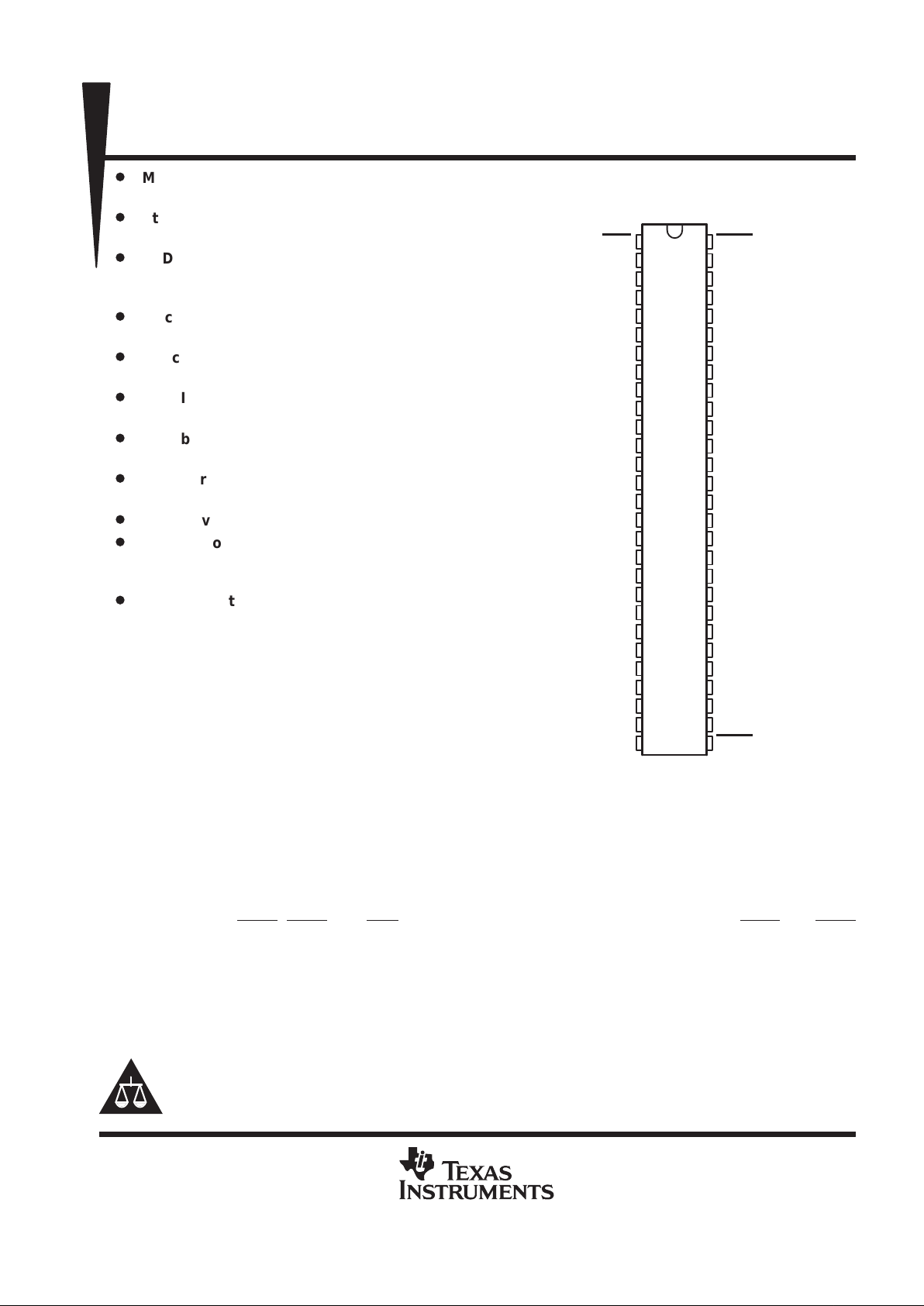
SN54ABT16260 . . . WD PACKAGE
SN74ABTH16260 . . . DL PACKAGE
(TOP VIEW)
1
2
3
4
5
6
7
8
9
10
11
12
13
14
15
16
17
18
19
20
21
22
23
24
25
26
27
28
56
55
54
53
52
51
50
49
48
47
46
45
44
43
42
41
40
39
38
37
36
35
34
33
32
31
30
29
OEA
LE1B
2B3
GND
2B2
2B1
V
CC
A1
A2
A3
GND
A4
A5
A6
A7
A8
A9
GND
A10
A11
A12
V
CC
1B1
1B2
GND
1B3
LE2B
SEL
OE2B
LEA2B
2B4
GND
2B5
2B6
V
CC
2B7
2B8
2B9
GND
2B10
2B11
2B12
1B12
1B11
1B10
GND
1B9
1B8
1B7
V
CC
1B6
1B5
GND
1B4
LEA1B
OE1B
SN54ABT16260, SN74ABTH16260
12-BIT TO 24-BIT MULTIPLEXED D-TYPE LATCHES
WITH 3-STATE OUTPUTS
SCBS204C – JUNE 1992 – REVISED MA Y 1997
2
POST OFFICE BOX 655303 • DALLAS, TEXAS 75265
description (continued)
When VCC is between 0 and 2.1 V , the device is in the high-impedance state during power up or power down.
However, to ensure the high-impedance state above 2.1 V, OE should be tied to VCC through a pullup resistor;
the minimum value of the resistor is determined by the current-sinking capability of the driver.
Active bus-hold circuitry is provided to hold unused or floating data inputs at a valid logic level.
The SN54ABT16260 is characterized for operation over the full military temperature range of –55°C to 125°C.
The SN74ABTH16260 is characterized for operation from –40°C to 85°C.
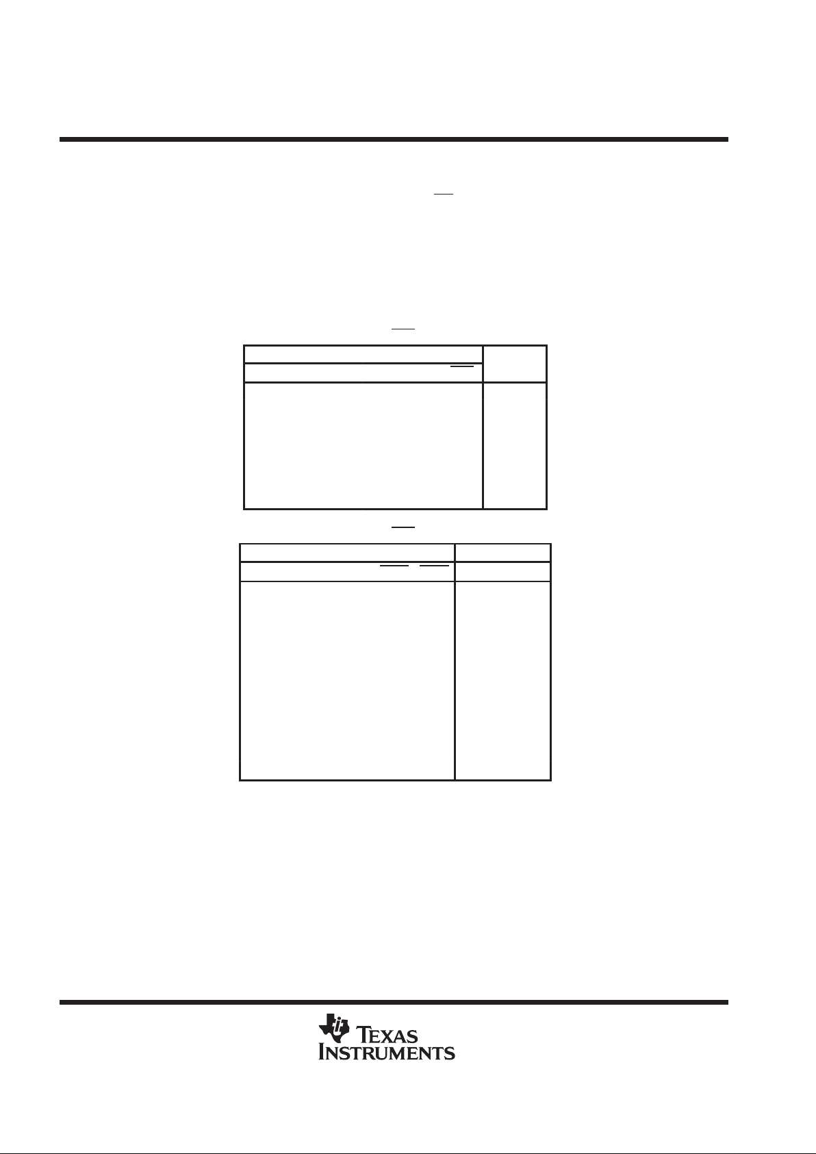
Function Tables
B TO A (OEB = H)
INPUTS
OUTPUT
1B 2B SEL LE1B LE2B OEA
A
H X H H X L H
L XHHXL L
X XHLXL A
0
X HLXHL H
X LLXHL L
X XLXLL A
0
X X X X X H Z
A TO B (OEA = H)
INPUTS
OUTPUTS
A LEA1B LEA2B OE1B OE2B 1B 2B
H H H L L H H
L HHLLLL
H HLLLH2B
0
L HLLLL2B
0
H LHLL1B0H
L LHLL1B0L
X LLLL1B02B
0
X XXHHZZ
X X X L H Active Z
X XXHLZActive
X X X L L Active Active
SN54ABT16260, SN74ABTH16260
12-BIT TO 24-BIT MULTIPLEXED D-TYPE LATCHES
WITH 3-STATE OUTPUTS
SCBS204C – JUNE 1992 – REVISED MA Y 1997
3
POST OFFICE BOX 655303 • DALLAS, TEXAS 75265
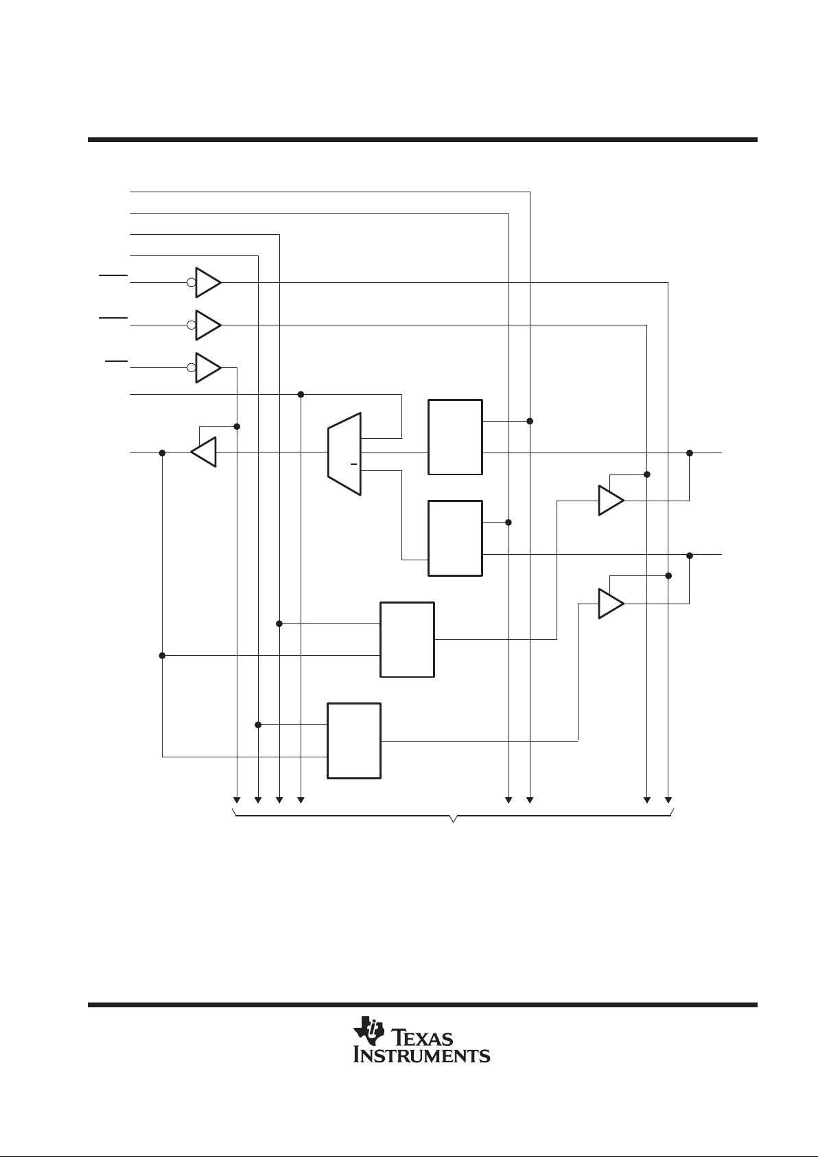
logic diagram (positive logic)
C1
1D
C1
1D
C1
1D
C1
1D
G1
To 11 Other Channels
LE1B
LE2B
LEA1B
LEA2B
OE2B
OE1B
OEA
SEL
A1 1B1
2B1
1
1
27
2
30
55
56
29
1
28
8
23
6
 Loading...