

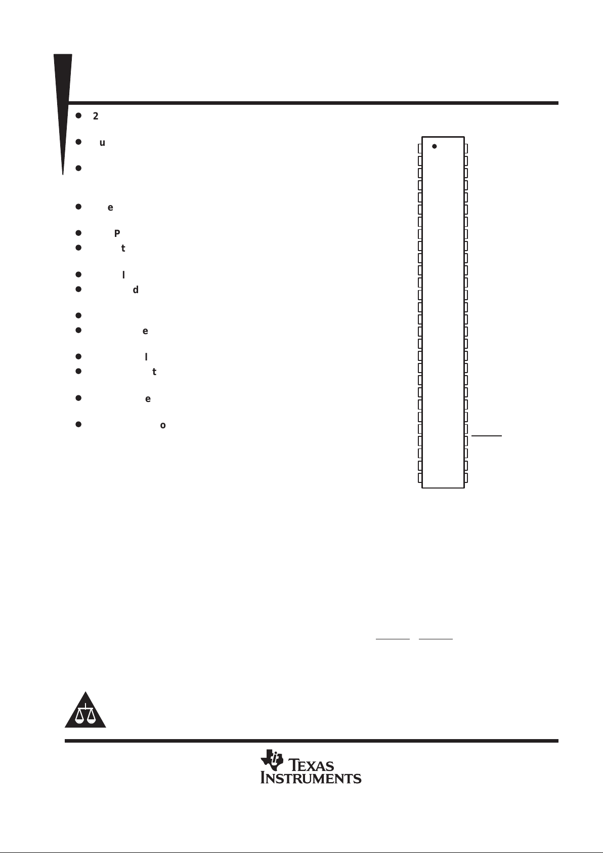
SN65LVDS93
LVDS SERDES TRANSMITTER
SLLS302F – MAY 1998 – REVISED FEBRUAR Y 2000
1
POST OFFICE BOX 655303 • DALLAS, TEXAS 75265
D
28:4 Data Channel Compression at up to
1.82 Gigabits per Second Throughput
D
Suited for Point-to-Point Subsystem
Communication With Very Low EMI
D
28 Data Channels Plus Clock in
Low-Voltage TTL and 4 Data Channels Plus
Clock Out Low-Voltage Differential
D
Selectable Rising or Falling Clock Edge
Triggered Inputs
D
Bus Pins Tolerate 6-kV HBM ESD
D
Operates From a Single 3.3-V Supply and
250 mW (Typ)
D
5-V Tolerant Data Inputs
D
Packaged in Thin Shrink Small-Outline
Package With 20 Mil Terminal Pitch
D
Consumes <1 mW When Disabled
D
Wide Phase-Lock Input Frequency Range
20 MHz to 65 MHz
D
No External Components Required for PLL
D
Outputs Meet or Exceed the Requirements
of ANSI EIA/TIA-644 Standard
D
Industrial Temperature Qualified
T
A
= –40°C to 85°C
D
Replacement for the DS90CR285
description
The SN65LVDS93 LVDS serdes (serializer/deserializer) transmitter contains four 7-bit parallelload serial-out shift registers, a 7× clock
synthesizer, and five low-voltage differential signaling (LVDS) drivers in a single integrated circuit. These
functions allow 28 bits of single-ended LVTTL data to be synchronously transmitted over five balanced-pair
conductors for receipt by a compatible receiver, such as the SN65LVDS94.
When transmitting, data bits D0 through D27 are each loaded into registers upon the edge of the input clock
signal (CLKIN). The rising or falling edge of the clock can be selected via the clock select (CLKSEL) pin. The
frequency of CLKIN is multiplied seven times and then used to serially unload the data registers in 7-bit slices.
The four serial streams and a phase-locked clock (CLKOUT) are then output to LVDS output drivers. The
frequency of CLKOUT is the same as the input clock, CLKIN.
The SN65LVDS93 requires no external components and little or no control. The data bus appears the same
at the input to the transmitter and output of the receiver with the data transmission transparent to the user(s).
The only user intervention is selecting a clock rising edge by inputting a high level to CLKSEL or a falling edge
with a low-level input and the possible use of the shutdown/clear (SHTDN
). SHTDN is an active-low input to
inhibit the clock and shut off the LVDS output drivers for lower power consumption. A low level on this signal
clears all internal registers at a low level.
The SN65LVDS93 is characterized for operation over ambient air temperatures of –40°C to 85°C.
Copyright 2000, Texas Instruments Incorporated
PRODUCTION DATA information is current as of publication date.
Products conform to specifications per the terms of Texas Instruments
standard warranty. Production processing does not necessarily include
testing of all parameters.
Please be aware that an important notice concerning availability, standard warranty, and use in critical applications of
Texas Instruments semiconductor products and disclaimers thereto appears at the end of this data sheet.
1
2
3
4
5
6
7
8
9
10
11
12
13
14
15
16
17
18
19
20
21
22
23
24
25
26
27
28
56
55
54
53
52
51
50
49
48
47
46
45
44
43
42
41
40
39
38
37
36
35
34
33
32
31
30
29
V
CC
D5
D6
D7
GND
D8
D9
D10
V
CC
D11
D12
D13
GND
D14
D15
D16
CLKSEL
D17
D18
D19
GND
D20
D21
D22
D23
V
CC
D24
D25
D4
D3
D2
GND
D1
D0
D27
LVDSGND
Y1M
Y1P
Y2M
Y2P
LVDSV
CC
LVDSGND
Y3M
Y3P
CLKOUTM
CLKOUTP
Y4M
Y4P
LVDSGND
PLLGND
PLLV
CC
PLLGND
SHTDN
CLKIN
D26
GND
DGG PACKAGE
(TOP VIEW)
SN65LVDS93
LVDS SERDES TRANSMITTER
SLLS302F – MAY 1998 – REVISED FEBRUAR Y 2000
2
POST OFFICE BOX 655303 • DALLAS, TEXAS 75265
functional block diagram
A,B, ...G
SHIFT/LOAD
CLK
Parallel-Load 7-Bit
Shift Register
7
A,B, ...G
SHIFT/LOAD
CLK
Parallel-Load 7-Bit
Shift Register
7
A,B, ...G
SHIFT/LOAD
CLK
Parallel-Load 7-Bit
Shift Register
7
A,B, ...G
SHIFT/LOAD
CLK
Parallel-Load 7-Bit
Shift Register
7
Control Logic
7×CLK
CLK
CLKINH
7× Clock/PLL
SHTDN
CLKIN
D5, D10, D11, D16,
D17, D23, D27
D19, D20, D21, D22,
D24, D25, D26
D8, D9, D12, D13,
D14, D15, D18
D0, D1, D2, D3,
D4, D6, D7
Y0P
Y0M
Y1P
Y1M
Y2P
Y2M
Y3P
Y3M
CLKOUTP
CLKOUTM
Input Bus
CLKSEL
RISING/FALLING
EDGE

SN65LVDS93
LVDS SERDES TRANSMITTER
SLLS302F – MAY 1998 – REVISED FEBRUAR Y 2000
3
POST OFFICE BOX 655303 • DALLAS, TEXAS 75265
CLKOUT
CLKIN
or
CLKIN
D0
Y0
Y1
Y2
Y3
D0–1 D7 D6 D4 D3 D2 D1 D0 D7+1
D8–1 D18 D15 D14 D13 D12 D9 D8 D18+1
D19–1 D26 D25 D24 D22 D21 D20 D19 D26+1
D27–1 D23 D17 D16 D11 D10 D5 D27 D23+1
Current Cycle
Next
Cycle
Previous Cycle
Figure 1. Typical ’LVDS93 Load and Shift Sequences
equivalent input and output schematic diagrams
V
CC
50 Ω
300 kΩ
7 V
Dn or
SHTDN
V
CC
7 V
10 kΩ
5 Ω
YnP or YnM
INPUT OUTPUT
SN65LVDS93
LVDS SERDES TRANSMITTER
SLLS302F – MAY 1998 – REVISED FEBRUAR Y 2000
4
POST OFFICE BOX 655303 • DALLAS, TEXAS 75265
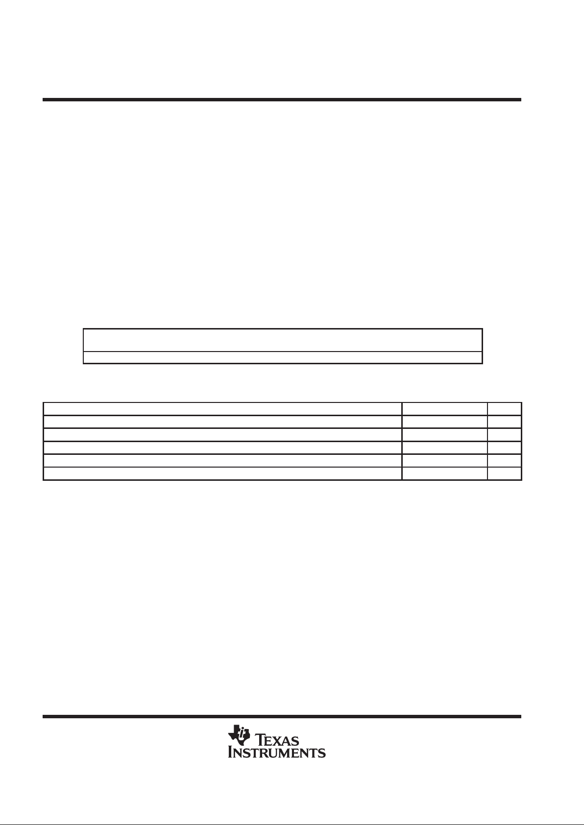
absolute maximum ratings over operating free-air temperature (unless otherwise noted)
†
Supply voltage range, VCC (see Note 1) –0.5 V to 4 V. . . . . . . . . . . . . . . . . . . . . . . . . . . . . . . . . . . . . . . . . . . . . .
Voltage range at any output terminal, VO –0.5 V to VCC + 0.5 V. . . . . . . . . . . . . . . . . . . . . . . . . . . . . . . . . . . . . . .
Voltage range at any input terminal, V
I
–0.5 V to 5.5 V. . . . . . . . . . . . . . . . . . . . . . . . . . . . . . . . . . . . . . . . . . . . . . .
Electrostatic discharge (see Note 2): Bus Pins (Class 3A) 6 KV. . . . . . . . . . . . . . . . . . . . . . . . . . . . . . . . . . . . .
Bus Pins (Class 2B) 400 V. . . . . . . . . . . . . . . . . . . . . . . . . . . . . . . . . . . .
Bus Pins (Class 2A) 6 KV. . . . . . . . . . . . . . . . . . . . . . . . . . . . . . . . . . . . .
Bus Pins (Class 2B) 200 V. . . . . . . . . . . . . . . . . . . . . . . . . . . . . . . . . . . .
Continuous total power dissipation See Dissipation Rating Table. . . . . . . . . . . . . . . . . . . . . . . . . . . . . . . . . . . . .
Operating free-air temperature range, T
A
–40°C to 85°C. . . . . . . . . . . . . . . . . . . . . . . . . . . . . . . . . . . . . . . . . . . .
Storage temperature range, T
stg
–65°C to 150°C. . . . . . . . . . . . . . . . . . . . . . . . . . . . . . . . . . . . . . . . . . . . . . . . . . .
Lead temperature 1,6 mm (1/16 inch) from case for 10 seconds 260°C. . . . . . . . . . . . . . . . . . . . . . . . . . . . . . .
†
Stresses beyond those listed under “absolute maximum ratings” may cause permanent damage to the device. These are stress ratings only, and
functional operation of the device at these or any other conditions beyond those indicated under “recommended operating conditions” is not
implied. Exposure to absolute-maximum-rated conditions for extended periods may affect device reliability.
NOTES: 1. All voltage values are with respect to the GND terminals.
2. This rating is measured using MIL-STD-883C Method, 3015.7.
DISSIPATION RATING T ABLE
PACKAGE
TA ≤ 25°C
POWER RATING
DERATING FACTOR
‡
ABOVE TA = 25°C
TA = 70°C
POWER RATING
TA = 85°C
POWER RATING
DGG 1377 mW 11 mW/°C 882 mW 717 mW
‡
This is the inverse of the junction-to-ambient thermal resistance when board-mounted and with no air flow.
recommended operating conditions
MIN NOM MAX UNIT
Supply voltage, V
CC
3 3.3 3.6 V
High-level input voltage, V
IH
2 V
Low-level input voltage, V
IL
0.8 V
Differential load impedance, Z
L
90 132 Ω
Operating free-air temperature, T
A
–40 85 °C

SN65LVDS93
LVDS SERDES TRANSMITTER
SLLS302F – MAY 1998 – REVISED FEBRUAR Y 2000
5
POST OFFICE BOX 655303 • DALLAS, TEXAS 75265
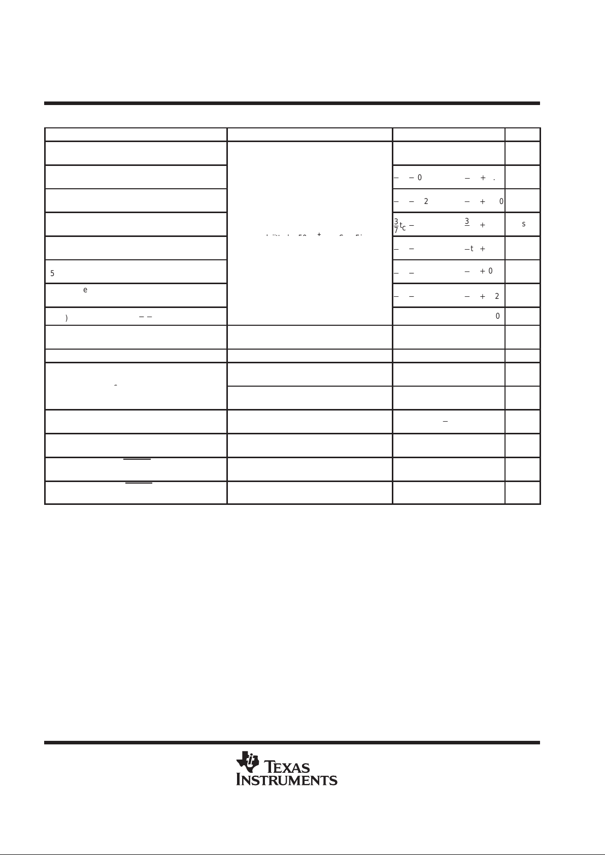
electrical characteristics over recommended operating free-air temperature range (unless
otherwise noted)
PARAMETER TEST CONDITIONS MIN TYP†MAX UNIT
V
T
Input voltage threshold 1.4 V
|VOD| Differential steady-state output voltage magnitude 247 454 mV
∆|VOD|
Change in the steady-state differential output
voltage magnitude between opposite binary states
RL = 100 Ω, See Figure 3
50 mV
V
OC(SS)
Steady-state common-mode output voltage See Figure 3 1.125 1.375 V
V
OC(PP)
Peak-to-peak common-mode output voltage 150 mV
I
IH
High-level input current VIH = V
CC
20 µA
I
IL
Low-level input current VIL = 0 V ±10 µA
p
VOY = 0 V ±24 mA
IOSShort-circuit output current
VOD = 0 V ±12 mA
I
OZ
High-impedance state output current VO = 0 V to V
CC
±20 µA
Disabled, All inputs at GND 350 µA
I
CC(AVG)
Quiescent current (average)
Enabled, RL = 100 Ω (5 places),
Worst-case pattern (see Figure 4),
tc = 15.38 ns
95 120 mA
C
i
Input capacitance 3 pF
†
All typical values are at VCC = 3.3 V, TA = 25°C.
timing requirements
MIN NOM MAX
UNIT
t
c
Input clock period 15.4 t
c
50 ns
t
w
High-level input clock pulse width duration 0.4t
c
0.6t
c
ns
t
t
Input signal transition time 5 ns
t
su
Data setup time, D0 through D27 before CLKIN↑ or CLKIN↓ (See Figure 2) 3 ns
t
h
Data hold time, D0 through D27 after CLKIN↓ or CLKIN↑ (See Figure 2) 1.5 ns
SN65LVDS93
LVDS SERDES TRANSMITTER
SLLS302F – MAY 1998 – REVISED FEBRUAR Y 2000
6
POST OFFICE BOX 655303 • DALLAS, TEXAS 75265
switching characteristics over recommended operating conditions (unless otherwise noted)
PARAMETER TEST CONDITIONS MIN TYP
†
MAX UNIT
t
0
Delay time, CLKOUT↑ to serial bit
position 0
–0.20 0 0.20 ns
t
1
Delay time, CLKOUT↑ to serial bit
position 1
1
7
tc*
0.20
1
7
tc)
0.20
ns
t
2
Delay time, CLKOUT↑ serial bit
position 2
2
7
tc*
0.20
2
7
tc)
0.20
ns
t
3
Delay time, CLKOUT↑ serial bit
position 3
tc = 15.38 ns (±0.2%),
3
7
tc*
0.20
3
7
tc)
0.20
ns
t
4
Delay time, CLKOUT↑ to serial bit
position 4
|Input clock jitter| < 50 ps‡, See Figure 5
4
7
tc*
0.20
4
7
tc)
0.20
ns
t
5
Delay time, CLKOUT↑ to serial bit
position 5
5
7
tc*
0.20
5
7
tc)
0.20
ns
t
6
Delay time, CLKOUT↑ to serial bit
position 6
6
7
tc*
0.20
6
7
tc)
0.20
ns
t
sk(o)
Output skew,
tn*
n
7
t
c
–0.20 0.20 ns
t
7
Delay time, CLKIN↓ or CLKIN↑ to
CLKOUT↑
tc = 15.38 ns (±0.2%),
|Input clock jitter| < 50 ps‡, See Figure 5
4.2 ns
t
c(o)
Output clock period t
c
ps
tc = 15.38 ns + 0.75sin(2π500E3t) ± 0.05 ns,
See Figure 6
±80 ps
∆t
c(o)
Output clock
cycle-to-cycle
jitt
er
§
tc = 15.38 ns + 0.75sin(2π3E6t) ± 0.05 ns,
See Figure 6
±300 ns
t
w
High-level output clock pulse duration
4
7
t
c
ps
t
t
Differential output voltage transition time
(tr or tf)
See Figure 3 260 700 1500 ps
t
en
Enable time, SHTDN↑ to phase lock
(Yn valid)
See Figure 7 1 ms
t
dis
Disable time, SHTDN↓ to off-state
(CLKOUT low)
See Figure 8 250 ns
†
All typical values are at VCC = 3.3 V, TA = 25°C.
‡
Input clock jitter is the magnitude of the charge in the input clock period
§
The output clock jitter is the change in the output clock period from one cycle to the next cycle observed over 15,000 cycles.

SN65LVDS93
LVDS SERDES TRANSMITTER
SLLS302F – MAY 1998 – REVISED FEBRUAR Y 2000
7
POST OFFICE BOX 655303 • DALLAS, TEXAS 75265
PARAMETER MEASUREMENT INFORMATION
Dn
t
su
CLKIN
t
h
CLKSEL LOW
CLKSEL HIGH
NOTE: All input timing is defined at 1.4 V on an input signal with a 10% to 90% rise or fall time of less than 5 ns.
Figure 2. Setup and Hold Time Definition
CL = 10 pF Max
(2 Places)
49.9 Ω ± 1% (2 Places)
V
OC
V
OD
YP
YM
V
OD(H)
V
OC(SS)
V
OC(SS)
V
OD(L)
100%
80%
20%
0%
0 V
V
OC(PP)
t
r
t
f
0 V
(a) SCHEMATIC
(b) WAVEFORMS
NOTE A: The lumped instrumentation capacitance for any
single-ended voltage measurement is less than or equal
to 10 pF . When making measurements at YP or YM, the
complementary output is similarly loaded.
Figure 3. Test Load and Voltage Definitions for LVDS Outputs

SN65LVDS93
LVDS SERDES TRANSMITTER
SLLS302F – MAY 1998 – REVISED FEBRUAR Y 2000
8
POST OFFICE BOX 655303 • DALLAS, TEXAS 75265
PARAMETER MEASUREMENT INFORMATION
t
c
NOTE A: The worst-case test pattern produces nearly the maximum switching frequency for all of the LVDS outputs. Pattern with
CLKSEL low shown.
CLKIN
Even Dn
Odd Dn
Figure 4. Worst-Case Test Pattern (CLKSEL low shown)
CLKIN
t
7
t
0
t
6
t
5
t
4
t
3
t
2
t
1
CLKOUT
Yn
V
OD(H)
V
OD(L)
0.00 V
td0 – t
d6
≈ 0.5 V
1.4 V
t
d7
CLKIN
≈ 2.5 V
CLKOUT
or
Yn
Figure 5. Timing Definitions

SN65LVDS93
LVDS SERDES TRANSMITTER
SLLS302F – MAY 1998 – REVISED FEBRUAR Y 2000
9
POST OFFICE BOX 655303 • DALLAS, TEXAS 75265
Reference
VCO
Device
Under
Test
Modulation
∑
+
+
V(t) = A sin (2 π f
(mod)
t)
HP8656B
Signal Generator
0.1 MHz – 990 MHz
HP8665A
Synthesized Signal
Generator
0.1 MHz – 4200 MHz
RF Output Modulation Input
Device Under Test DTS2070C
Digital Time Scope
OUTPUT CLKIN CLKOUT Input
Figure 6. Output Clock Jitter Test Setup
CLKIN
t
en
SHTDN
Dn
Yn
ValidInvalid
Figure 7. Enable Time Waveforms (CLKSEL low shown)
CLKIN
CLKOUT
t
dis
SHTDN
Figure 8. Disable Time Waveforms (CLKSEL low shown)

SN65LVDS93
LVDS SERDES TRANSMITTER
SLLS302F – MAY 1998 – REVISED FEBRUAR Y 2000
10
POST OFFICE BOX 655303 • DALLAS, TEXAS 75265
TYPICAL CHARACTERISTICS
I
CC
60
40
20
0
30 40 50 60 70
80
100
f – Frequency – MHz
– Supply Current – mA
WORST-CASE SUPPLY CURRENT
vs
FREQUENCY
120
VCC = 3.6 V
VCC = 3 V
VCC = 3.3 V
Figure 9

SN65LVDS93
LVDS SERDES TRANSMITTER
SLLS302F – MAY 1998 – REVISED FEBRUAR Y 2000
11
POST OFFICE BOX 655303 • DALLAS, TEXAS 75265
APPLICATION INFORMATION
16-bit bus extension
In a 16-bit bus application (Figure 10), TTL data and clock coming from bus transceivers that interface the
backplane bus arrive at the Tx parallel inputs of the L VDS serdestransmitter. The clock associated with the bus
is also connected to the device. The on-chip PLL synchronizes this clock with the parallel data at the input. The
data is then multiplexed into three different line drivers which perform the TTL to LVDS conversion. The clock
is also converted to L VDS and presented to a separate driver. This synchronized LVDS data and clock at the
receiver, which recovers the LVDS data and clock, performs a conversion back to TTL. Data is then
demultiplexed into a parallel format. An on-chip PLL synchronizes the received clock with the parallel data, and
then all are presented to the parallel output port of the receiver.
SN74FB2032
8
D0–D7
8
D8–D15
SN65LVDS93
LVDS
Interface
0 To 10 Meters
(Media Dependent)
TTL
Interface
16-Bit
BTL Bus
Interface
CLK
Backplane
Bus
8
D0–D7
8
D8–D15
CLK
Backplane
Bus
TTL
Interface
16-Bit
BTL Bus
Interface
XMIT Clock RCV Clock
SN74FB2032
SN65LVDS94
SN74FB2032
SN74FB2032
Figure 10. 16-Bit Bus Extension
16-bit bus extension with parity
In the previous application we did not have a checking bit that would provide assurance that the data crosses
the link. If we add a parity bit to the previous example, we would have a diagram similar to the one in Figure 11.
The device following the SN74FB2032 is a low-cost parity generator. Each transmit-side transceiver/parity
generator takes the L VTTL data from the corresponding transceiver, performs a parity calculation over the byte,
and then passes the bits with its calculated parity value on the parallel input of the LVDS serdes transmitter.
Again, the on-chip PLL synchronizes this transmit clock with the eighteen parallel bits (16 data + 2 parity) at the
input. The synchronized LVDS data/parity and clock arrive at the receiver.
The receiver performs the conversion from L VDS to LVTTL and the transceiver/parity generator performs the
parity calculations. These devices compare their corresponding input bytes with the value received on the parity
bit. The transceiver/parity generator will assert its parity error output if a mismatch is detected.

SN65LVDS93
LVDS SERDES TRANSMITTER
SLLS302F – MAY 1998 – REVISED FEBRUAR Y 2000
12
POST OFFICE BOX 655303 • DALLAS, TEXAS 75265
APPLICATION INFORMATION
SN74FB2032
8
D0–D7
8
D8–D15
SN65LVDS93
LVDS
Interface
0 To 10 Meters
(Media Dependent)
TTL
Interface
W/Parity
16-Bit
BTL Bus
Interface
CLK
Backplane
Bus
8
D0–D7
8
D8–D15
CLK
Backplane
Bus
TTL
Interface
16-Bit
BTL Bus
Interface
XMIT Clock RCV Clock
9 Bit Latchable
Transceiver/ With
Parity Generator
Parity
Parity
TTL
Interface
Parity
Parity
Parity
Error
TTL
Interface
W/Parity
SN74FB2032
9 Bit Latchable
Transceiver/ With
Parity Generator
SN74FB2032
SN74FB2032
9 Bit Latchable
Transceiver/ With
Parity Generator
9 Bit Latchable
Transceiver/ With
Parity Generator
SN65LVDS94
Figure 11. 16-Bit Bus Extension With Parity
low cost virtual backplane transceiver
Figure 12 represents L VDS serdes in an application as a virtual backplane transceiver (VBT). The concept of
a VBT can be achieved by implementing individual LVDS serdes chipsets in both directions of subsystem
serialized links.
Depending on the application, the designer will face varying choices when implementing a VBT. In addition to
the devices shown in Figure 12, functions such as parity and delay lines for control signals could be included.
Using additional circuitry, half-duplex or full-duplex operation can be achieved by configuring the clock and
control lines properly.
The designer may choose to implement an independent clock oscillator at each end of the link and then use
a PLL to synchronize LVDS serdes’s parallel I/O to the backplane bus. Resynchronizing FIFOs may also be
required.
Bus
Transceivers
LVDS Serdes
Transmitter
LVDS Serdes
Receiver
Bus
Transceivers
TTL
Inputs
Up To
21 or 28
Bits
LVDS
Serial Links
4 or 5
Pairs
TTL
Outputs
Up To
21 or 28
Bits
Bus
Transceivers
LVDS Serdes
Transmitter
LVDS Serdes
Receiver
Bus
Transceivers
Backplane
Bus
Backplane
Bus
Figure 12. Virtual Backplane Transceiver

SN65LVDS93
LVDS SERDES TRANSMITTER
SLLS302F – MAY 1998 – REVISED FEBRUAR Y 2000
13
POST OFFICE BOX 655303 • DALLAS, TEXAS 75265
MECHANICAL DATA
DGG (R-PDSO-G**) PLASTIC SMALL-OUTLINE PACKAGE
4040078/F 12/97
48 PIN SHOWN
0,25
0,15 NOM
Gage Plane
6,00
6,20
8,30
7,90
0,75
0,50
Seating Plane
25
0,27
0,17
24
A
48
1
1,20 MAX
M
0,08
0,10
0,50
0°–8°
56
14,10
13,90
48
DIM
A MAX
A MIN
PINS **
12,40
12,60
64
17,10
16,90
0,15
0,05
NOTES: A. All linear dimensions are in millimeters.
B. This drawing is subject to change without notice.
C. Body dimensions do not include mold protrusion not to exceed 0,15.
D. Falls within JEDEC MO-153

IMPORTANT NOTICE
T exas Instruments and its subsidiaries (TI) reserve the right to make changes to their products or to discontinue
any product or service without notice, and advise customers to obtain the latest version of relevant information
to verify, before placing orders, that information being relied on is current and complete. All products are sold
subject to the terms and conditions of sale supplied at the time of order acknowledgement, including those
pertaining to warranty, patent infringement, and limitation of liability.
TI warrants performance of its semiconductor products to the specifications applicable at the time of sale in
accordance with TI’s standard warranty. Testing and other quality control techniques are utilized to the extent
TI deems necessary to support this warranty. Specific testing of all parameters of each device is not necessarily
performed, except those mandated by government requirements.
CERT AIN APPLICATIONS USING SEMICONDUCTOR PRODUCTS MAY INVOLVE POTENTIAL RISKS OF
DEATH, PERSONAL INJURY, OR SEVERE PROPERTY OR ENVIRONMENTAL DAMAGE (“CRITICAL
APPLICATIONS”). TI SEMICONDUCTOR PRODUCTS ARE NOT DESIGNED, AUTHORIZED, OR
WARRANTED TO BE SUITABLE FOR USE IN LIFE-SUPPORT DEVICES OR SYSTEMS OR OTHER
CRITICAL APPLICATIONS. INCLUSION OF TI PRODUCTS IN SUCH APPLICA TIONS IS UNDERSTOOD T O
BE FULLY AT THE CUSTOMER’S RISK.
In order to minimize risks associated with the customer’s applications, adequate design and operating
safeguards must be provided by the customer to minimize inherent or procedural hazards.
TI assumes no liability for applications assistance or customer product design. TI does not warrant or represent
that any license, either express or implied, is granted under any patent right, copyright, mask work right, or other
intellectual property right of TI covering or relating to any combination, machine, or process in which such
semiconductor products or services might be or are used. TI’s publication of information regarding any third
party’s products or services does not constitute TI’s approval, warranty or endorsement thereof.
Copyright 2000, Texas Instruments Incorporated
 Loading...