

Texas Instruments SN65LVDS387DGG, SN65LVDS387DGGR, SN65LVDS389DBT, SN65LVDS389DBTR, SN75LVDS389DBT Datasheet
...
SN65LVDS387, SN75LVDS387, SN65LVDS389, SN75LVDS389
HIGH-SPEED DIFFERENTIAL LINE DRIVERS
SLLS362B – SEPTEMBER 1999 – REVISED NOVEMBER 1999
D
Eight (’389) or Sixteen (’387) Line Drivers
Meet or Exceed the Requirements of ANSI
EIA/TIA-644 Standard
D
Designed for Signaling Rates up to
630 Mbps With Very Low Radiation (EMI)
D
Low-Voltage Differential Signaling With
Typical Output Voltage of 350 mV and a
100 Ω Load
D
Propagation Delay Times Less Than 2.9 ns
D
Output Skew Is Less Than 150 ps
D
Part-to-Part Skew Is Less Than 1.5 ns
D
35 mW Total Power Dissipation in Each
Driver Operating at 200 MHz
D
Driver is High Impedance When Disabled or
With VCC < 1.5 V
D
SN65’ Version Bus-Pin ESD Protection
Exceeds 12 kV
D
Packaged in Thin Shrink Small-Outline
Package With 20-mil Terminal Pitch
D
Low-Voltage TTL (LVTTL) Logic Inputs Are
5-V Tolerant
description
The SN65L VDS389 and SN75L VDS389 are eight
and the SN65LVDS387 and SN75LVDS387 are
sixteen differential line drivers that implement the
electrical characteristics of low-voltage differential
signalling (LVDS). This signaling technique lowers the output voltage levels of 5-V differential
standard levels (such as EIA/TIA-422B) to reduce
the power, increase the switching speeds, and allow operation with a 3.3-V supply rail. Any of the
sixteen current-mode drivers will deliver a minimum differential output voltage magnitude of
247 mV into a 100-Ω load when enabled.
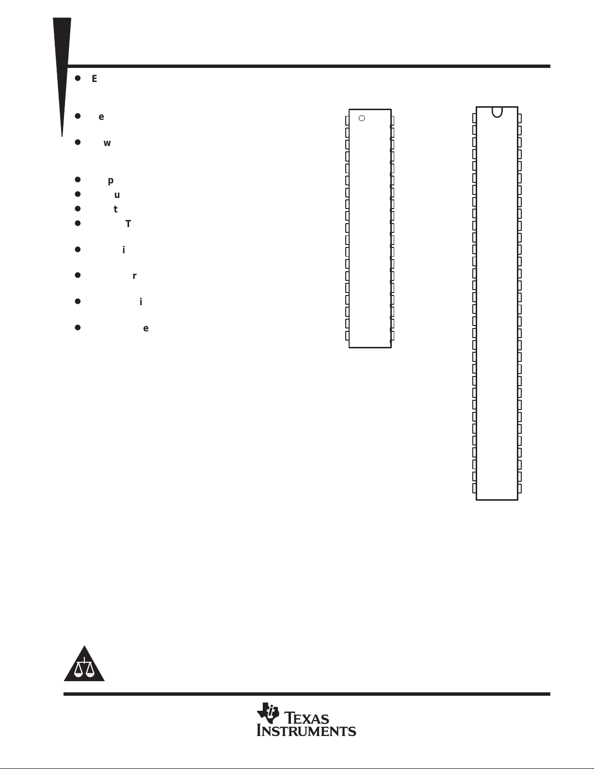
DBT PACKAGE
(TOP VIEW)
GND
V
CC
GND
ENA
A1A
A2A
A3A
A4A
GND
V
CC
GND
B1A
B2A
B3A
B4A
ENB
GND
V
CC
GND
’LVDS389
1
38
2
37
3
36
4
35
5
34
6
33
7
32
8
31
9
30
10
29
11
28
12
27
13
26
14
25
15
24
16
23
17
22
18
21
19
20
A1Y
A1Z
A2Y
A2Z
A3Y
A3Z
A4Y
A4Z
NC
NC
NC
B1Y
B1Z
B2Y
B2Z
B3Y
B3Z
B4Y
B4Z
DGG PACKAGE
(TOP VIEW)
GND
V
CC
V
CC
GND
ENA
A1A
A2A
A3A
A4A
ENB
B1A
B2A
B3A
B4A
GND
V
CC
V
CC
GND
C1A
C2A
C3A
C4A
ENC
D1A
D2A
D3A
D4A
END
GND
V
CC
V
CC
GND
’LVDS387
1
2
3
4
5
6
7
8
9
10
11
12
13
14
15
16
17
18
19
20
21
22
23
24
25
26
27
28
29
30
31
32
64
63
62
61
60
59
58
57
56
55
54
53
52
51
50
49
48
47
46
45
44
43
42
41
40
39
38
37
36
35
34
33
A1Y
A1Z
A2Y
A2Z
A3Y
A3Z
A4Y
A4Z
B1Y
B1Z
B2Y
B2Z
B3Y
B3Z
B4Y
B4Z
C1Y
C1Z
C2Y
C2Z
C3Y
C3Z
C4Y
C4Z
D1Y
D1Z
D2Y
D2Z
D3Y
D3Z
D4Y
D4Z
The intended application of this device and signaling technique is for point-to-point and multidrop baseband data
transmission over controlled impedance media of approximately 100 Ω. The transmission media can be
printed-circuit board traces, backplanes, or cables. The large number of drivers integrated into the same
substrate, along with the low pulse skew of balanced signaling, allows extremely precise timing alignment of
clock and data for synchronous parallel data transfers. When used with the companion 16- or 8-channel
receivers, the SN65LVDS386 or SN65LVDS388, over 300 million data transfers per second in single-edge
clocked systems are possible with very little power. (Note: The ultimate rate and distance of data transfer is
dependent upon the attenuation characteristics of the media, the noise coupling to the environment, and other
system characteristics.)
Please be aware that an important notice concerning availability, standard warranty, and use in critical applications of
Texas Instruments semiconductor products and disclaimers thereto appears at the end of this data sheet.
TI is a trademark of Texas Instruments Incorporated.
PRODUCTION DATA information is current as of publication date.
Products conform to specifications per the terms of Texas Instruments
standard warranty. Production processing does not necessarily include
testing of all parameters.
POST OFFICE BOX 655303 • DALLAS, TEXAS 75265
Copyright 1999, Texas Instruments Incorporated
1
SN65LVDS387, SN75LVDS387, SN65LVDS389, SN75LVDS389
HIGH-SPEED DIFFERENTIAL LINE DRIVERS
SLLS362B – SEPTEMBER 1999 – REVISED NOVEMBER 1999
description (continued)
The drivers are enabled in groups of four and are designated as banks A, B, C, and D. When disabled, the driver
outputs are a high impedance. Each driver input (A) and enable (EN) have an internal pulldown that will drive
the input to a low level when open circuited.
The SN65LVDS387 and SN65LVDS389 are characterized for operation from –40°C to 85°C. The
SN75LVDS387 and SN75LVDS389 are characterized for operation from 0°C to 70°C.
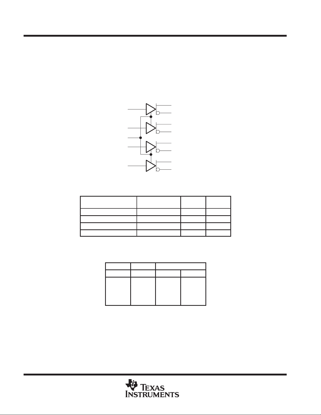
logic diagram (positive logic)
1A
2A
EN
3A
4A
(1/4 of ’LVDS387 or 1/2 of ’LVDS389 shown)
AVAILABLE OPTIONS
PART NUMBER
SN65LVDS387DGG –40°C to 85°C 16 12 kV
SN75LVDS387DGG 0°C to 70°C 16 4 kV
SN65LVDS389DBT –40°C to 85°C 8 12 kV
SN75LVDS389DBT 0°C to 70°C 8 4 kV
†
This package is available taped and reeled. To order this packaging option, add
an R suffix to the part number (e.g., SN65LVDS387DGGR).
†
TEMPERATURE
RANGE
DRIVER FUNCTION TABLE
1Y
1Z
2Y
2Z
3Y
3Z
4Y
4Z
NO. OF
DRIVERS
BUS-PIN
ESD
INPUT
A EN Y Z
H H H L
L H L H
X L Z Z
OPEN H L H
H = high-level, L = low-level, X = irrelevant,
Z = high-impedance (off)
2
POST OFFICE BOX 655303 • DALLAS, TEXAS 75265
ENABLE OUTPUTS

O erating free-air tem erature, T
A
SN65LVDS387, SN75LVDS387, SN65LVDS389, SN75LVDS389
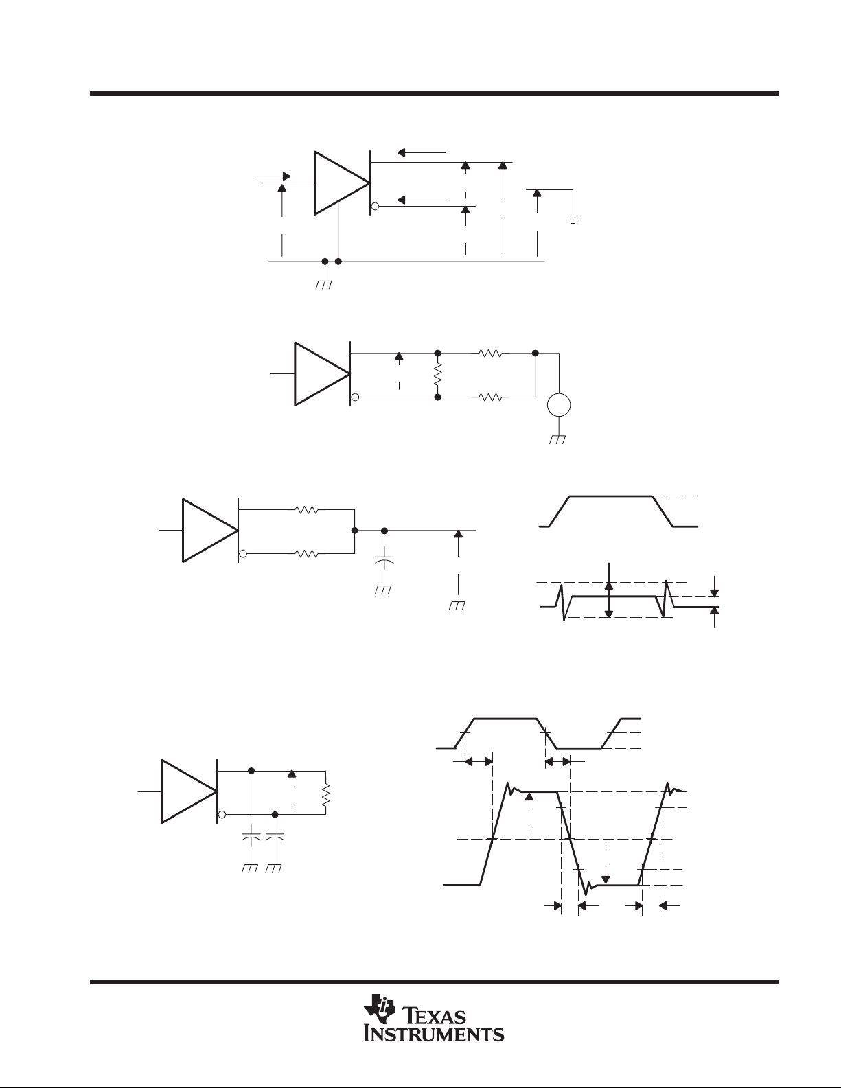
equivalent input and output schematic diagrams
EQUIVALENT OF EACH A OR EN INPUT TYPICAL OF ALL OUTPUTS
V
CC
HIGH-SPEED DIFFERENTIAL LINE DRIVERS
SLLS362B – SEPTEMBER 1999 – REVISED NOVEMBER 1999
V
CC
7 V
50 Ω
10 kΩ
300 kΩ
–0.5 V to 4 V. . . . . . . . . . . . . . . . . . . . . . . . . . . . . . . . . . . . . . . . . . . . . . . . . . . . . . . . . .
CC
5 Ω
Y or Z
Output
7 V
†
A or EN
Input
absolute maximum ratings over operating free-air temperature (unless otherwise noted)
Supply voltage range, V
Input voltage range: Inputs –0.5 V to 6 V. . . . . . . . . . . . . . . . . . . . . . . . . . . . . . . . . . . . . . . . . . . . . . . . . . . . . . . . .
Y or Z –0.5 V to 4 V. . . . . . . . . . . . . . . . . . . . . . . . . . . . . . . . . . . . . . . . . . . . . . . . . . . . . . . . .
Electrostatic discharge: SN65’ (Y, Z, and GND) Class 3, A:12 kV, B: 500 V. . . . . . . . . . . . . . . . . . . . . . . . . . . .
SN65’ (All pins) Class 3, A: 4 kV, B:400 V. . . . . . . . . . . . . . . . . . . . . . . . . . . . . . . . . . . .
SN75’ (Y, Z, and GND) Class 3, A:4 kV, B: 400 V. . . . . . . . . . . . . . . . . . . . . . . . . . . . . .
SN75’ (All pins) Class 2, A: 2 kV, B:200 V. . . . . . . . . . . . . . . . . . . . . . . . . . . . . . . . . . . .
Continuous power dissipation (see Dissipation Rating Table). . . . . . . . . . . . . . . . . . . . . . . . . . . . . . . . . . . . . . . .
Storage temperature range –65°C to 150°C. . . . . . . . . . . . . . . . . . . . . . . . . . . . . . . . . . . . . . . . . . . . . . . . . . . . . . . .
Lead temperature 1,6 mm (1/16 in) from case for 10 seconds 260°C. . . . . . . . . . . . . . . . . . . . . . . . . . . . . . . . . .
†
Stresses beyond those listed under “absolute maximum ratings” may cause permanent damage to the device. These are stress ratings only, and
functional operation of the device at these or any other conditions beyond those indicated under “recommended operating conditions” is not
implied. Exposure to absolute-maximum-rated conditions for extended periods may affect device reliability.
NOTES: 1. All voltage values, except differential I/O bus voltages, are with respect to network ground terminal.
‡
This is the inverse of the junction-to-ambient thermal resistance when board-mounted (low-k) and with no air flow.
2. Tested in accordance with MIL-STD-883C Method 3015.7.
DISSIPATION RATING TABLE
PACKAGE
DBT 1071 mW 8.5 mW/°C 688 mW 556 mW
DGG 2094 mW 16.7 mW/°C 1342 mW 1089 mW
TA ≤ 25°C
DERATING FACTOR
ABOVE TA = 25°C
‡
TA = 70°C
POWER RATING
TA = 85°C
POWER RATING
recommended operating conditions
Supply voltage, V
High-level input voltage, V
Low-level input voltage, V
p
MIN NOM MAX UNIT
CC
IH
IL
p
POST OFFICE BOX 655303 • DALLAS, TEXAS 75265
SN75’ 0 70 °C
SN65’ –40 85 °C
3 3.3 3.6 V
2 V
0.8 V
3

SN65LVDS387, SN75LVDS387, SN65LVDS389, SN75LVDS389
R
100 Ω
R
100 Ω
ICCSu ly current
mA
,
IOSShort-circuit output current
R
L
100 Ω
L
See Figure 5
HIGH-SPEED DIFFERENTIAL LINE DRIVERS
SLLS362B – SEPTEMBER 1999 – REVISED NOVEMBER 1999
electrical characteristics over recommended operating conditions (unless otherwise noted)
PARAMETER TEST CONDITIONS MIN TYP†MAX UNIT
|VOD| Differential output voltage magnitude
∆|VOD|
V
OC(SS)
∆V
OC(SS)
V
OC(PP)
I
I
IH
I
IL
I
OZ
I
O(OFF)
C
IN
C
O
†
All typical values are at 25°C and with a 3.3 V supply.
Change in differential output voltage
magnitude between logic states
Steady-state common-mode output voltage 1.125 1.375 V
Change in steady-state common-mode output
voltage between logic states
Peak-to-peak common-mode output voltage 50 150 mV
Supply current
High-level input current VIH = 2 V 3 20 µA
Low-level input current VIL = 0.8 V 2 10 µA
p
High-impedance output current VO = 0 V or V
Power-off output current VCC = 1.5 V, VO = 2.4 V ±1 µA
Input capacitance VI = 0.4 sin (4E6πt) + 0.5 V 5 pF
Output capacitance
=
L
See Figure 1 and 2
See 3
’LVDS387
’LVDS389
’LVDS387
’LVDS389
VOY or VOZ = 0 V ±24 mA
VOD = 0 V ±12 mA
VI = 0.4 sin (4E6πt) + 0.5 V,
Disabled
,,
CC
Enabled,
=
L
VIN = 0.8 V or 2 V
Disabled,
VIN = 0 V or V
,
CC
247 340 454
–50 50
–50 50 mV
85 95
50 70
0.5 1.5
0.5 1.5
±1 µA
9.4 pF
mV
mA
switching characteristics over recommended operating conditions (unless otherwise noted)
PARAMETER TEST CONDITIONS MIN TYP†MAX UNIT
t
PLH
t
PHL
t
r
t
f
t
sk(p)
t
sk(o)
t
sk(pp)
t
PZH
t
PZL
t
PHZ
t
PLZ
†
All typical values are at 25°C and with a 3.3 V supply.
‡
t
sk(o)
§
t
sk(pp)
with the same supply voltages, at the same temperature, and have identical packages and test circuits.
Propagation delay time, low-to-high-level output 0.9 1.7 2.9 ns
Propagation delay time, high-to-low-level output 0.9 1.6 2.9 ns
Differential output signal rise time
Differential output signal fall time
Pulse skew (|t
Output skew
Part-to-part skew
Propagation delay time, high-impedance-to-high-level output 6.4 15 ns
Propagation delay time, high-impedance-to-low-level output
Propagation delay time, high-level-to-high-impedance output
Propagation delay time, low-level-to-high-impedance output 4.5 15 ns
is the magnitude of the time difference between the t
is the magnitude of the difference in propagation delay times between any specified terminals of two devices when both devices operate
‡
PHL
– t
|)
PLH
§
or t
PLH
of all drivers of a single device with all of their inputs connected together.
PHL
=
CL = 10 pF,
See Figure 4
,
0.4 0.8 1 ns
0.4 0.8 1 ns
150 500 ps
80 150 ps
1.5 ns
5.9 15 ns
3.5 15 ns
4
POST OFFICE BOX 655303 • DALLAS, TEXAS 75265
SN65LVDS387, SN75LVDS387, SN65LVDS389, SN75LVDS389
HIGH-SPEED DIFFERENTIAL LINE DRIVERS
SLLS362B – SEPTEMBER 1999 – REVISED NOVEMBER 1999
PARAMETER MEASUREMENT INFORMATION
I
OY
GND
Y
V
I
OZ
Z
OD
V
OY
V
V
OZ
OC
(VOY + VOZ)/2
I
I
A
V
I
Figure 1. Voltage and Current Definitions
Input
Y
V
OD
Z
100 Ω
3.75 kΩ
3.75 kΩ
±
0 V ≤ V
TEST
≤ 2.4 V
Figure 2. VOD Test Circuit
49.9 Ω ± 1% (2 Places)
Y
V
Input
Z
50 pF
NOTE: All input pulses are supplied by a generator having the following characteristics: tr or tf ≤ 1 ns, Pulse Repetition Rate (PRR) = 0.5 Mpps,
Pulse width = 500 ± 10 ns . CL includes instrumentation and fixture capacitance within 0,06 m of the D.U.T . The measurement of V
is made on test equipment with a –3 dB bandwidth of at least 300 MHz.
V
OC
I
V
OC(PP)
V
O
3 V
0 V
V
OC(SS)
OC(PP)
Figure 3. Test Circuit and Definitions for the Driver Common-Mode Output V oltage
Input
t
Y
PLH
t
PHL
2 V
1.4 V
0.8 V
Input
Z
NOTE: All input pulses are supplied by a generator having the following characteristics: tr or tf ≤ 1 ns, Pulse Repetition Rate (PRR) = 50 Mpps,
Pulse width = 10 ± 0.2 ns . CL includes instrumentation and fixture capacitance within 0,06 m of the D.U.T.
V
OD
CL = 10 pF
(2 Places)
100 Ω ± 1 %
Output
0 V
V
OD(H)
V
OD(L)
t
f
t
r
100%
80%
20%
0%
Figure 4. Test Circuit, Timing, and Voltage Definitions for the Differential Output Signal
POST OFFICE BOX 655303 • DALLAS, TEXAS 75265
5

SN65LVDS387, SN75LVDS387, SN65LVDS389, SN75LVDS389
HIGH-SPEED DIFFERENTIAL LINE DRIVERS
SLLS362B – SEPTEMBER 1999 – REVISED NOVEMBER 1999
PARAMETER MEASUREMENT INFORMATION
Y
0.8 V or 2 V
Input
Input
t
PZH
V
OY
or
V
OZ
t
PZL
V
OZ
or
V
OY
NOTE: All input pulses are supplied by a generator having the following characteristics: tr or tf ≤ 1 ns, Pulse Repetition Rate (PRR) = 0.5 Mpps,
Pulse width = 500 ± 10 ns . CL includes instrumentation and fixture capacitance within 0,06 m of the D.U.T.
Z
CL = 10 pF
(2 Places)
49.9 Ω ± 1% (2 Places)
V
OYVOZ
2 V
1.4 V
0.8 V
t
PHZ
≅ 1.4 V
1.3 V
1.2 V
t
PLZ
1.2 V
1.1 V
≅ 1 V
+
1.2 V
–
Figure 5. Enable and Disable Time Circuit and Definitions
6
POST OFFICE BOX 655303 • DALLAS, TEXAS 75265
SN65LVDS387, SN75LVDS387, SN65LVDS389, SN75LVDS389
HIGH-SPEED DIFFERENTIAL LINE DRIVERS
SLLS362B – SEPTEMBER 1999 – REVISED NOVEMBER 1999
TYPICAL CHARACTERISTICS
’L VDS387
SUPPLY CURRENT (RMS)
vs
SWITCHING FREQUENCY
240
220
200
180
160
140
– Supply Current – mA
CC
120
I
100
80
0 50 100 150 200 250 300 350
VCC = 3.6 V
VCC = 3.3 V
VCC = 3 V
All outputs loaded and enabled.
f – Frequency – MHz
Figure 6
’L VDS389
SUPPLY CURRENT (RMS)
vs
SWITCHING FREQUENCY
110
100
90
80
70
– Supply Current – mA
60
CC
I
50
40
VCC = 3.6 V
VCC = 3.3 V
VCC = 3 V
All outputs loaded and enabled.
0 50 100 150 200 250 300
f – Frequency – MHz
Figure 7
LOW-TO-HIGH PROPAGATION DELAY TIME
vs
FREE-AIR TEMPERATURE
2.1
2.0
1.9
1.8
1.7
1.6
1.5
1.4
PLH – Low-To-High Propagation Delay Time – ns
t
1.3
–40 –20 0 20 40 60 80 100
VCC = 3.6 V
VCC = 3 V
VCC = 3.3 V
TA – Free-Air Temperature – °C
Figure 8
HIGH-TO-LOW PROPAGATION DELAY TIME
vs
FREE-AIR TEMPERATURE
2.2
2.0
VCC = 3 V
1.8
1.6
1.4
1.2
PHL – High-To-Low Propagation Delay Time – ns
t
1.0
–40 –20 0 20 40 60 80 100
Ta – Free-Air Temperature – °C
VCC = 3.3 V
VCC = 3.6 V
Figure 9
POST OFFICE BOX 655303 • DALLAS, TEXAS 75265
7
SN65LVDS387, SN75LVDS387, SN65LVDS389, SN75LVDS389
HIGH-SPEED DIFFERENTIAL LINE DRIVERS
SLLS362B – SEPTEMBER 1999 – REVISED NOVEMBER 1999
TYPICAL CHARACTERISTICS
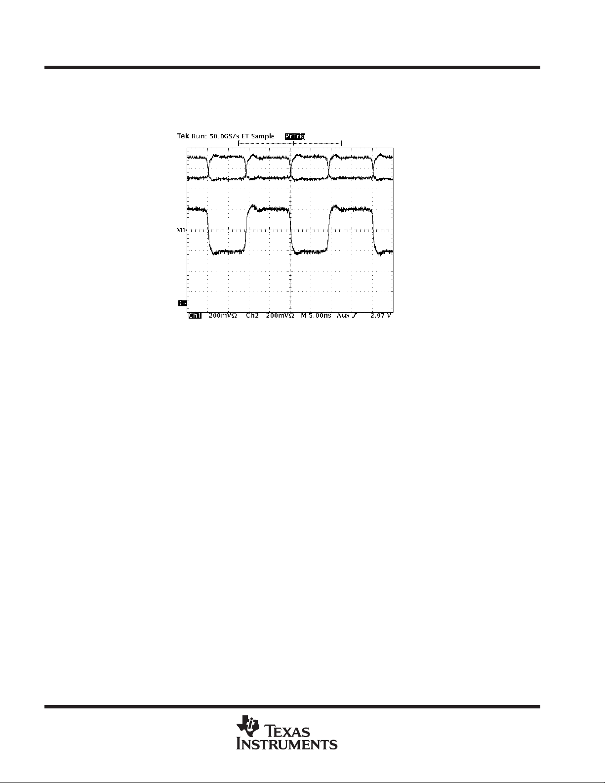
OUTPUT VOLTAGE
vs
TIME
V
OY
V
OZ
V
OD
– Output Voltage – V
O
V
t – Time – ns
Figure 10
8
POST OFFICE BOX 655303 • DALLAS, TEXAS 75265

SN65LVDS387, SN75LVDS387, SN65LVDS389, SN75LVDS389
HIGH-SPEED DIFFERENTIAL LINE DRIVERS
SLLS362B – SEPTEMBER 1999 – REVISED NOVEMBER 1999
APPLICATION INFORMATION
Host
Host
Controller
DBn
DBn–1
DBn–2
DBn–3
DB2
DB1
DB0
TX Clock
SN65LVDS387 or 389
Power Power
Balanced Interconnect
T
T
T
T
T
T
T
T
Indicates twisting of the
conductors.
Target
DBn
Target
Controller
DBn–1
DBn–2
DBn–3
DB2
DB1
DB0
RX Clock
LVDS Receiver(s)
Indicates the line termination
T
circuit.
Figure 11. Typical Application Schematic
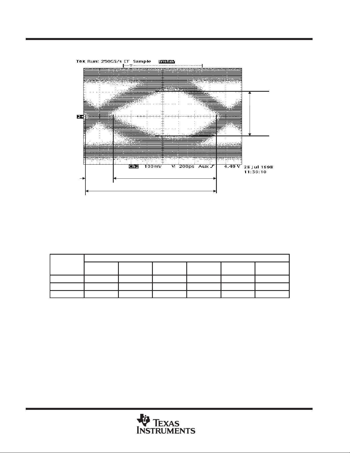
Signaling Rate vs Distance
The ultimate data transfer rate over a given cable or trace length involves many variables. Starting with the
capabilities of this LVDS driver to reproduce a data pulse as short as 1.6 ns (a 630 Mbps signaling rate) with
less than 500 ps of pulse distortion, any degradation of this pulse by the transmission media will necessarily
reduce the the timing margin at the receiving end of the data link.
The timing uncertainty induced by the transmission media is commonly referred to as jitter and comes from
numerous sources. The characteristics of a particular transmission media can be quantified by using an
eyepattern measurement such as shown in Figure 12, which shows about 340 ps of jitter or 20% of the data
pulse width.
POST OFFICE BOX 655303 • DALLAS, TEXAS 75265
9
SN65LVDS387, SN75LVDS387, SN65LVDS389, SN75LVDS389
LENGTH
HIGH-SPEED DIFFERENTIAL LINE DRIVERS
SLLS362B – SEPTEMBER 1999 – REVISED NOVEMBER 1999
APPLICATION INFORMATION
abs.
jitter
width
height
unit interval
Figure 12. Typical LVDS Eyepattern
A generally accepted range of jitter at the receiver inputs that allows data recovery is 5% to 20% of the unit
interval (data pulse width). Table 1 shows the signaling rate achieved on various cables and lengths at a 5%
eyepattern jitter with a typical LVDS driver.
Table 1. Signaling Rates for Various Cables for 5% Eyepattern Jitter
†
CABLE
(m)
1 240 200 240 270 180 230
5 205 210 230 250 215 230
10 180 150 195 200 145 180
†
Cable A: CAT 3, specified up to 16 MHz, no shield, outside conductor diameter (∅) 0.52 mm
Cable B: CAT 5, specified up to 100 MHz, no shield, ∅ 0.52 mm
Cable C: CAT 5, specified up to 100 MHz, taped over all shield, ∅ 0.52 mm
Cable D: CAT 5 (exceeding CAT 5), specified up to 300 MHz, braided over all shield plus taped individual shield for
Cable E: CAT 5 (exceeding CAT 5), specified up to 350 MHz, ∅ 0.64 mm (AWG22), no shield
Cable F: CAT 5 (exceeding CAT 5), specified up to 350 MHz, “self-shielded”, ∅0.64 mm (A WG22)
A
(Mbps)
any pair, ∅ 0.64 mm (AWG22)
B
(Mbps)
C
(Mbps)
D
(Mbps)
E
(Mbps)
F
(Mbps)
During synchronous parallel transfers, skew between the data and clock lines will also reduce the timing margin.
This must be accounted for in the system timing budget. Fortunately, the low output skew of this L VDS driver
will generally be a small portion of this budget.
other LVDS products
For other products and applications notes in the LVDS and LVDM product families visit our Web site at
http://www.ti.com/sc/datatran.
10
POST OFFICE BOX 655303 • DALLAS, TEXAS 75265
SN65LVDS387, SN75LVDS387, SN65LVDS389, SN75LVDS389
HIGH-SPEED DIFFERENTIAL LINE DRIVERS
SLLS362B – SEPTEMBER 1999 – REVISED NOVEMBER 1999
MECHANICAL DATA
DBT (R-PDSO-G**) PLASTIC SMALL-OUTLINE PACKAGE
30 PINS SHOWN
0,50
30
1
1,20 MAX
0,27
0,17
16
4,50
4,30
15
A
Seating Plane
0,15
0,05
0,08
M
0,15 NOM
6,60
6,20
Gage Plane
0,25
0°–8°
0,75
0,50
0,10
PINS **
DIM
A MAX
A MIN
NOTES: A. All linear dimensions are in millimeters.
B. This drawing is subject to change without notice.
C. Body dimensions do not include mold flash or protrusion.
D. Falls within JEDEC MO-153
28
7,90
7,70
30
7,90
7,70
38
9,80 11,10
44
50
12,60
12,409,60 10,90
4073252/D 09/97
POST OFFICE BOX 655303 • DALLAS, TEXAS 75265
11

SN65LVDS387, SN75LVDS387, SN65LVDS389, SN75LVDS389
HIGH-SPEED DIFFERENTIAL LINE DRIVERS
SLLS362B – SEPTEMBER 1999 – REVISED NOVEMBER 1999
MECHANICAL DATA
DGG (R-PDSO-G**) PLASTIC SMALL-OUTLINE PACKAGE
48 PINS SHOWN
0,50
48
1
1,20 MAX
0,27
0,17
25
24
A
0,15
0,05
0,08
M
8,30
6,20
7,90
6,00
Seating Plane
0,10
0,15 NOM
Gage Plane
0,25
0°–8°
0,75
0,50
DIM
NOTES: A. All linear dimensions are in millimeters.
B. This drawing is subject to change without notice.
C. Body dimensions do not include mold protrusion not to exceed 0,15.
D. Falls within JEDEC MO-153
PINS **
A MAX
A MIN
48
12,60
12,40
56
14,10
13,90
64
17,10
16,90
4040078/F 12/97
12
POST OFFICE BOX 655303 • DALLAS, TEXAS 75265

IMPORTANT NOTICE
T exas Instruments and its subsidiaries (TI) reserve the right to make changes to their products or to discontinue
any product or service without notice, and advise customers to obtain the latest version of relevant information
to verify, before placing orders, that information being relied on is current and complete. All products are sold
subject to the terms and conditions of sale supplied at the time of order acknowledgement, including those
pertaining to warranty, patent infringement, and limitation of liability.
TI warrants performance of its semiconductor products to the specifications applicable at the time of sale in
accordance with TI’s standard warranty. Testing and other quality control techniques are utilized to the extent
TI deems necessary to support this warranty . Specific testing of all parameters of each device is not necessarily
performed, except those mandated by government requirements.
CERTAIN APPLICA TIONS USING SEMICONDUCTOR PRODUCTS MA Y INVOLVE POTENTIAL RISKS OF
DEATH, PERSONAL INJURY, OR SEVERE PROPERTY OR ENVIRONMENTAL DAMAGE (“CRITICAL
APPLICATIONS”). TI SEMICONDUCTOR PRODUCTS ARE NOT DESIGNED, AUTHORIZED, OR
WARRANTED TO BE SUITABLE FOR USE IN LIFE-SUPPORT DEVICES OR SYSTEMS OR OTHER
CRITICAL APPLICA TIONS. INCLUSION OF TI PRODUCTS IN SUCH APPLICATIONS IS UNDERST OOD TO
BE FULLY AT THE CUSTOMER’S RISK.
In order to minimize risks associated with the customer’s applications, adequate design and operating
safeguards must be provided by the customer to minimize inherent or procedural hazards.
TI assumes no liability for applications assistance or customer product design. TI does not warrant or represent
that any license, either express or implied, is granted under any patent right, copyright, mask work right, or other
intellectual property right of TI covering or relating to any combination, machine, or process in which such
semiconductor products or services might be or are used. TI’s publication of information regarding any third
party’s products or services does not constitute TI’s approval, warranty or endorsement thereof.
Copyright 1999, Texas Instruments Incorporated
 Loading...