

Texas Instruments SN65LVDS388DBT, SN65LVDS388DBTR, SN65LVDT386DGG, SN65LVDT386DGGR, SN65LVDT388DBT Datasheet
...
SN65LVDS386, SN65LVDT386, SN75LVDS386, SN75LVDT386
SN65LVDS388, SN65LVDT388, SN75LVDS388, SN75LVDT388
HIGH-SPEED DIFFERENTIAL LINE RECEIVERS
SLLS394A – SEPTEMBER 1999 – REVISED DECEMBER 1999
D
Eight (‘388) or Sixteen (‘386) Line Receivers
Meet or Exceed the Requirements of ANSI
TIA/EIA-644 Standard
D
Integrated 110-Ω Line Termination
Resistors on LVDT Products
D
Designed for Signaling Rates† Up To
630 Mbps
D
SN65 Version’s Bus-Terminal ESD Exceeds
15 kV
D
Operates From a Single 3.3-V Supply
D
Typical Propagation Delay Time of 2.6 ns
D
Output Skew 100 ps (Typ)
Part-To-Part Skew is Less Than 1 ns
D
LVTTL Levels are 5-V Tolerant
D
Open-Circuit Fail Safe
D
Flow-Through Pin Out
D
Packaged in Thin Shrink Small-Outline
Package With 20-mil Terminal Pitch
description
The ‘LVDS388 and ‘LVDT388 (T designates
integrated termination) are eight and the
‘LVDS386 and ‘LVDT386 sixteen differential line
receivers respectively that implement the electrical characteristics of low-voltage differential
signaling (L VDS). This signaling technique lowers
the output voltage levels of 5-V differential
standard levels (such as EIA/TIA-422B) to reduce
the power, increase the switching speeds, and
allow operation with a 3-V supply rail. Any of the
eight or sixteen differential receivers will provide
a valid logical output state with a ±100 mV
differential input voltage within the input commonmode voltage range. The input common-mode
voltage range allows 1 V of ground potential
difference between two L VDS nodes. Additionally ,
the high-speed switching of L VDS signals almost
always require the use of a line impedance
matching resistor at the receiving end of the cable
or transmission media. The LVDT products
eliminate this external resistor by integrating it
with the receiver.
SN65LVDS388, SN75LVDS388
SN65LVDT388, SN75LVDT388
DBT PACKAGE
(TOP VIEW)
1
38
37
36
35
34
33
32
31
30
29
28
27
26
25
24
23
22
21
20
GND
V
CC
ENA
A1Y
A2Y
ENB
B1Y
B2Y
GND
V
CC
GND
C1Y
C2Y
ENC
D1Y
D2Y
END
V
CC
GND
A1A
A1B
A2A
A2B
NC
B1A
B1B
B2A
B2B
NC
C1A
C1B
C2A
C2B
NC
D1A
D1B
D2A
D2B
2
3
4
5
6
7
8
9
10
11
12
13
14
15
16
17
18
19
SN65LVDS386, SN75LVDS386
SN65LVDT386, SN75LVDT386
DGG PACKAGE
(TOP VIEW)
1
64
63
62
61
60
59
58
57
56
55
54
53
52
51
50
49
48
47
46
45
44
43
42
41
40
39
38
37
36
35
34
33
GND
V
CC
V
CC
GND
ENA
A1Y
A2Y
A3Y
A4Y
ENB
B1Y
B2Y
B3Y
B4Y
GND
V
CC
V
CC
GND
C1Y
C2Y
C3Y
C4Y
ENC
D1Y
D2Y
D3Y
D4Y
END
GND
V
CC
V
CC
GND
A1A
A1B
A2A
A2B
A3A
A3B
A4A
A4B
B1A
B1B
B2A
B2B
B3A
B3B
B4A
B4B
C1A
C1B
C2A
C2B
C3A
C3B
C4A
C4B
D1A
D1B
D2A
D2B
D3A
D3B
D4A
D4B
2
3
4
5
6
7
8
9
10
11
12
13
14
15
16
17
18
19
20
21
22
23
24
25
26
27
28
29
30
31
32
Please be aware that an important notice concerning availability, standard warranty, and use in critical applications of
Texas Instruments semiconductor products and disclaimers thereto appears at the end of this data sheet.
†
Signaling rate, 1/t, where t is the minimum unit interval and is expressed in the units bits/s (bits per second)
PRODUCTION DATA information is current as of publication date.
Products conform to specifications per the terms of Texas Instruments
standard warranty. Production processing does not necessarily include
testing of all parameters.
POST OFFICE BOX 655303 • DALLAS, TEXAS 75265
Copyright 1999, Texas Instruments Incorporated
1

SN65LVDS386, SN65LVDT386, SN75LVDS386, SN75LVDT386
SN65LVDS388, SN65LVDT388, SN75LVDS388, SN75LVDT388
HIGH-SPEED DIFFERENTIAL LINE RECEIVERS
SLLS394A – SEPTEMBER 1999 – REVISED DECEMBER 1999
description (continued)
The intended application of this device and signaling technique is for point-to-point baseband data transmission
over controlled impedance media of approximately 100 Ω. The transmission media may be printed circuit board
traces, backplanes, or cables. The large number of receivers integrated into the same substrate along with the
low pulse skew of balanced signaling, allows extremely precise timing alignment of clock and data for
synchronous parallel data transfers. When used with its companion, 8- or 16-channel driver, the SN65LVDS389
or SN65L VDS387, over 300 million data transfers per second in single-edge clocked systems are possible with
very little power. (Note: The ultimate rate and distance of data transfer is dependent upon the attenuation
characteristics of the media, the noise coupling to the environment, and other system characteristics.)
Available Options
Part number
SN65LVDS386DGG
SN65LVDT386DGG
SN75LVDS386DGG
SN75LVDT386DGG
SN65LVDS388DBT
SN65LVDT388DBT
SN75LVDS388DBT
SN75LVDT388DBT
Temperature
Range
–40_C to 85_C
–40_C to 85_C
0_C to 70_C
0_C to 70_C
–40_C to 85_C
–40_C to 85_C
0_C to 70_C
0_C to 70_C
Number of
Receivers
16 15 kV
16 15 kV
16 4 kV
16 4 kV
8 15 kV
8 15 kV
8 4 kV
8 4 kV
Bus-Pin ESD
logic diagram (positive logic)
’LVDx386
’LVDT386 ONLY
1A
1B
2A
2B
EN
3A
3B
4A
4B
H = high level, L = low level, X = irrelevant,
Z = high impedance (off), ? = indeterminate
1Y
2Y
3Y
4Y
’LVDT388 ONLY
1A
1B
EN
2A
2B
’LVDx388
Function Table
SNx5LVD386/388 and SNx5LVDT386/388
DIFFERENTIAL INPUT
A-B EN Y
VID ≥ 100 mV H H
-100 mV < VID ≤ 100 mV H ?
VID≤ -100 mV H L
X L Z
Open H H
ENABLES OUTPUT
1Y
2Y
2
POST OFFICE BOX 655303 • DALLAS, TEXAS 75265
SN65LVDS386, SN65LVDT386, SN75LVDS386, SN75LVDT386
SN65LVDS388, SN65LVDT388, SN75LVDS388, SN75LVDT388
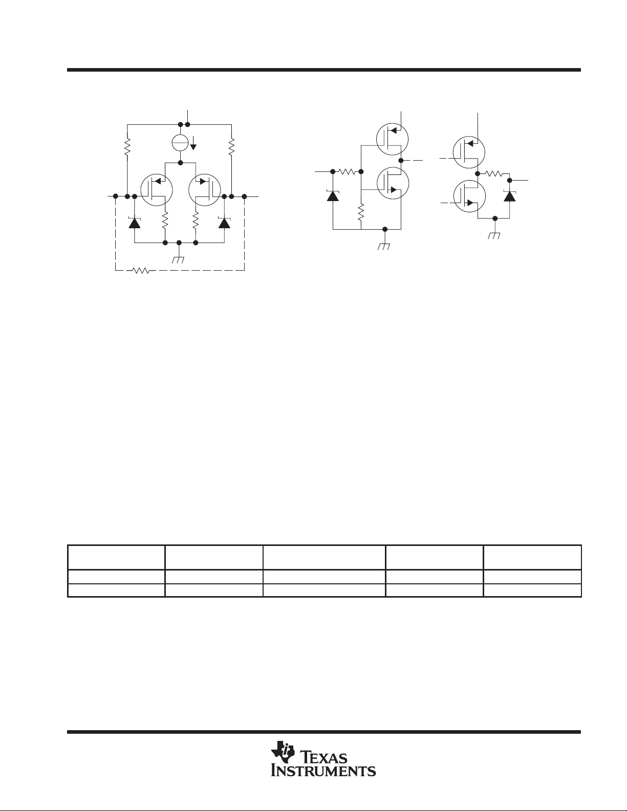
equivalent input and output schematic diagrams
HIGH-SPEED DIFFERENTIAL LINE RECEIVERS
SLLS394A – SEPTEMBER 1999 – REVISED DECEMBER 1999
V
CC
300 kΩ300 kΩ
EN
A Input B Input
7 V 7 V
110 Ω
’LVDT Devices Only
100 Ω
7 V
absolute maximum ratings over operating free-air temperature (unless otherwise noted)
300 kΩ
V
CC
V
CC
5 Ω
Y Output
7 V
†
Supply voltage range, VCC (see Note 1) –0.5 V to 4 V. . . . . . . . . . . . . . . . . . . . . . . . . . . . . . . . . . . . . . . . . . . . . .
Voltage range: Enables or Y –0.5 V to VCC + 2 V. . . . . . . . . . . . . . . . . . . . . . . . . . . . . . . . . . . . . . . . . . . . .
A or B –0.5 V to 4 V. . . . . . . . . . . . . . . . . . . . . . . . . . . . . . . . . . . . . . . . . . . . . . . . . . . . . . . . .
Electrostatic discharge: (see Note 2)
SN65’ (A, B, and GND) Class 3, A:15 kV, B: 700 V. . . . . . . . . . . . . . . . . . . . . . . . . . . .
SN65’ (All pins) Class 3, A: 8 kV, B:600 V. . . . . . . . . . . . . . . . . . . . . . . . . . . . . . . . . . . .
SN75’ (A, B, and GND) Class 2, A:4 kV, B: 400 V. . . . . . . . . . . . . . . . . . . . . . . . . . . . .
SN75’ (All pins) Class 2, A: 2 kV, B:200 V. . . . . . . . . . . . . . . . . . . . . . . . . . . . . . . . . . . .
Continuous power dissipation See Dissipation Rating Table. . . . . . . . . . . . . . . . . . . . . . . . . . . . . . . . . . . . . . . . .
Storage temperature range –65°C to 150°C. . . . . . . . . . . . . . . . . . . . . . . . . . . . . . . . . . . . . . . . . . . . . . . . . . . . . . . .
Lead temperature 1,6 mm (1/16 in) from case for 10 seconds 260°C. . . . . . . . . . . . . . . . . . . . . . . . . . . . . . . . . .
†
Stresses beyond those listed under “absolute maximum ratings” may cause permanent damage to the device. These are stress ratings only, and
functional operation of the device at these or any other conditions beyond those indicated under “recommended operating conditions” is not
implied. Exposure to absolute-maximum-rated conditions for extended periods may affect device reliability.
NOTES: 1. All voltage values, except differential I/O bus voltages, are with respect to network ground terminal.
‡
This is the inverse of the junction-to-ambient thermal resistance when board-mounted (low-k) and with no air flow.
2. Tested in accordance with MIL-STD-883C Method 3015.7.
DISSIPATION RATING TABLE
PACKAGE
DBT 1071 mW 8.5 mW/°C 688 mW 556 mW
DGG 2094 mW 16.7 mW/°C 1342 mW 1089 mW
TA ≤ 25°C
DERATING FACTOR
ABOVE TA = 25°C
‡
TA = 70°C
POWER RATING
TA = 85°C
POWER RATING
POST OFFICE BOX 655303 • DALLAS, TEXAS 75265
3
SN65LVDS386, SN65LVDT386, SN75LVDS386, SN75LVDT386
O erating free-air tem erature, T
A
SN65LVDS388, SN65LVDT388, SN75LVDS388, SN75LVDT388
HIGH-SPEED DIFFERENTIAL LINE RECEIVERS
SLLS394A – SEPTEMBER 1999 – REVISED DECEMBER 1999
recommended operating conditions
MIN NOM MAX UNIT
Supply voltage, V
High-level input voltage, V
Low-level input voltage, V
Magnitude of differential input voltage, VID 0.1 0.6 V
Common–mode input voltage, VIC (see Figure 4)
p
CC
IH
IL
p
SN75’ 0 70 °C
SN65’ –40 85 °C
3 3.3 3.6 V
2 V
|VID|
2
2.4
*
VCC – 0.8
0.8 V
|VID|
2
V
4
POST OFFICE BOX 655303 • DALLAS, TEXAS 75265
See Figure 1 and Table 1
I
Supply current
mA
’LVDS
I
Input current (A or B inputs)
A
’LVDT
I
High–impedance output current
A
g
See Figure 3
SN65LVDS386, SN65LVDT386, SN75LVDS386, SN75LVDT386
SN65LVDS388, SN65LVDT388, SN75LVDS388, SN75LVDT388
HIGH-SPEED DIFFERENTIAL LINE RECEIVERS
SLLS394A – SEPTEMBER 1999 – REVISED DECEMBER 1999
electrical characteristics over recommended operating conditions (unless otherwise noted).
PARAMETER TEST CONDITIONS MIN TYP†MAX UNIT
V
ITH+
V
ITH–
V
OH
V
OL
CC
I
I
ID
I
ID
I
I(OFF)
I
I(OFF)
I
IH
I
IL
OZ
C
IN
Z
(t)
†
All typical values are at 25°C and with a 3.3 V supply.
Positive–going differential input voltage threshold
Negative–going differential input voltage threshold
High–level output voltage IOH = –8 mA 2.4 3 V
Low–level output voltage IOL = 8 mA 0.2 0.4 V
pp
’
p
Differential input current |IIA – IIB| ‘LVDS
Differential input current (IIA – IIB) ‘LVDT
Power–off Input current (A or B inputs) ‘LVDS VCC = 0 V, VI=2.4 V 12 ±20 µA
Power–off Input current (A or B inputs) ‘LVDT VCC = 0 V, VI=2.4 V ±40 µA
High–level input current (enables) VIH = 2 V 10 µA
Low–level input current (enables) VIL = 0.8 V 10 µA
p
Input Capacitance, A or B input to GND VID = 0.4 sin 2.5E09 t V 5 pF
T ermination impedance VID = 0.4 sin 2.5E09 t V 88 132 Ω
p
’
p
Enabled, No load 50 70
Disabled 3
VI = 0 V –13 –20
VI = 2.4 V –1.2 –3
VI = 0 V, other input open –40
VI = 2.4 V, other input open –2.4
VIA= 0 V, VIB = 0.1V,
VIA= 2.4 V, VIB = 2.3 V
VIA= 0.2 V, VIB = 0V,
VIA= 2.4 V, VIB = 2.2 V
VO = 0 V ±1
VO = 3.6 V 10
–100 mV
1.5 2.2 mA
100 mV
±2 µA
µ
µ
switching characteristics over recommended operating conditions (unless otherwise noted)
PARAMETER TEST CONDITIONS MIN TYP†MAX UNIT
t
PLH
t
PHL
t
r
t
f
t
sk(p)
t
sk(o)
t
sk(pp)
t
PZH
t
PZL
t
PHZ
t
PLZ
†
All typical values are at 25°C and with a 3.3 V supply.
‡
t
sk(o)
§
t
sk(pp)
with the same supply voltages, at the same temperature, and have identical packages and test circuits.
Propagation delay time, low-to-high-level output 1 2.6 4 ns
Propagation delay time, high-to-low-level output 1 2.5 4 ns
Differential output signal rise time 500 800 1200 ps
Differential output signal fall time
Pulse skew (|t
Output skew
Part-to-part skew
Propagation delay time, high-impedance-to-high-level output 7 15 ns
Propagation delay time, high-impedance-to-low-level output
Propagation delay time, high-level-to-high-impedance output
Propagation delay time, low-level-to-high-impedance output 7 15 ns
is the magnitude of the time difference between the t
is the magnitude of the difference in propagation delay times between any specified terminals of two devices when both devices operate
‡
PHL
– t
|)
PLH
§
or t
PLH
of all drivers of a single device with all of their inputs connected together.
PHL
See Figure 2
500 800 1200 ps
150 600 ps
100 400 ps
1 ns
7 15 ns
7 15 ns
POST OFFICE BOX 655303 • DALLAS, TEXAS 75265
5

SN65LVDS386, SN65LVDT386, SN75LVDS386, SN75LVDT386
SN65LVDS388, SN65LVDT388, SN75LVDS388, SN75LVDT388
HIGH-SPEED DIFFERENTIAL LINE RECEIVERS
SLLS394A – SEPTEMBER 1999 – REVISED DECEMBER 1999
PARAMETER MEASUREMENT INFORMATION
A
VIA)
V
IB
2
V
IA
V
IC
Figure 1. Voltage Definitions
Table 1. Receiver Minimum and Maximum Input Threshold Test Voltages
V
ID
B
V
IB
R
V
O
Applied Voltages
V
IA
1.25 V 1.15 V 100 mV 1.2 V
1.15 V 1.25 V –100 mV 1.2 V
2.4 V 2.3 V 100 mV 2.35 V
2.3 V 2.4 V –100 mV 2.35 V
0.1 V 0 V 100 mV 0.05 V
0 V 0.1 V –100 mV 0.05 V
1.5 V 0.9 V 600 mV 1.2 V
0.9 V 1.5 V –600 mV 1.2 V
2.4 V 1.8 V 600 mV 2.1 V
1.8 V 2.4 V –600 mV 2.1 V
0.6 V 0 V 600 mV 0.3 V
0 V 0.6 V –600 mV 0.3 V
V
IB
Resulting Differential
Input Voltage
V
ID
Resulting Common–
Mode Input Voltage
V
IC
6
POST OFFICE BOX 655303 • DALLAS, TEXAS 75265

SN65LVDS386, SN65LVDT386, SN75LVDS386, SN75LVDT386
SN65LVDS388, SN65LVDT388, SN75LVDS388, SN75LVDT388
HIGH-SPEED DIFFERENTIAL LINE RECEIVERS
SLLS394A – SEPTEMBER 1999 – REVISED DECEMBER 1999
PARAMETER MEASUREMENT INFORMATION
V
ID
V
IA
V
IB
C
L
10 pF
V
O
V
IA
V
IB
V
ID
t
PHL
V
O
NOTE: All input pulses are supplied by a generator having the following characteristics: tr or tf ≤ 1 ns, Pulse Repetition Rate (PRR) = 50 Mpps,
Pulse width = 10 ± 0.2 ns . CL includes instrumentation and fixture capacitance within 0,06 m of the D.U.T.
2.4 V
0.4 V
t
f
t
PLH
t
r
1.4 V
1 V
0.4 V
0 V
–0.4 V
V
OH
1.4 V
V
OL
Figure 2. Timing Test Circuit and Wave Forms
POST OFFICE BOX 655303 • DALLAS, TEXAS 75265
7

SN65LVDS386, SN65LVDT386, SN75LVDS386, SN75LVDT386
SN65LVDS388, SN65LVDT388, SN75LVDS388, SN75LVDT388
HIGH-SPEED DIFFERENTIAL LINE RECEIVERS
SLLS394A – SEPTEMBER 1999 – REVISED DECEMBER 1999
PARAMETER MEASUREMENT INFORMATION
1.2 V
Inputs
NOTE A: All input pulses are supplied by a generator having the following characteristics: tr or tf ≤ 1 ns, pulse repetition rate (PRR) = 0.5 Mpps,
pulse width = 500 ± 10 ns. CL includes instrumentation and fixture capacitance within 0,06 m of the D.U.T.
V
TEST
A
EN
t
PZL
EN
B
500 Ω
A
C
L
10 pF
V
O
t
PLZ
+
–
V
2.5 V
1 V
2 V
1.4 V
0.8 V
TEST
2.5 V
1.4 V
V
OL
0 V
1.4 V
2 V
1.4 V
0.8 V
V
OH
1.4 V
0 V
V
TEST
EN
Y
A
Y
VOL +0.5 V
t
PZH
VOH –0.5 V
t
PHZ
Figure 3. Enable/Disable Time Test Circuit and Wave Forms
8
POST OFFICE BOX 655303 • DALLAS, TEXAS 75265

SN65LVDS386, SN65LVDT386, SN75LVDS386, SN75LVDT386
SN65LVDS388, SN65LVDT388, SN75LVDS388, SN75LVDT388
HIGH-SPEED DIFFERENTIAL LINE RECEIVERS
SLLS394A – SEPTEMBER 1999 – REVISED DECEMBER 1999
TYPICAL CHARACTERISTICS
LVDx388
SUPPLY CURRENT
vs
SWITCHING FREQUENCY
2.5
COMMON-MODE INPUT VOLTAGE
vs
DIFFERENTIAL INPUT VOLTAGE
200
Max at VCC > 3.15 V
180
2.0
1.5
1.0
– Common-Mode Input Voltage – V
0.5
IC
V
0
4.0
3.5
3.0
2.5
2.0
Max at VCC = 3 V
Minimum
0 0.1 0.2 0.3 0.4 0.5 0.6
|VID| – Differential Input Voltage – V
Figure 4
HIGH-LEVEL OUTPUT VOLTAGE
vs
HIGH-LEVEL OUTPUT CURRENT
160
140
120
100
80
– Supply Current – mA
60
CC
I
40
20
0
0 20 40 60 80 100 120 140 160 180 200
f – Switching Frequency – MHz
LOW-LEVEL OUTPUT VOLTAGE
LOW-LEVEL OUTPUT CURRENT
5.0
4.5
4.0
3.5
3.0
2.5
VCC = 3.6 V
VCC = 3 V
VCC = 3.3 V
Figure 5
vs
1.5
1.0
– High-Level Output Voltage – V
OH
V
0.5
0
–70 –60 –50 –40 –30 –20 –10 0
IOH – High-Level Output Current – mA
Figure 6
POST OFFICE BOX 655303 • DALLAS, TEXAS 75265
2.0
1.5
1.0
OL
V – Low-Level Output Voltage – V
0.5
0
0 1020304050607080
IOL – Low-Level Output Current – mA
Figure 7
9

SN65LVDS386, SN65LVDT386, SN75LVDS386, SN75LVDT386
SN65LVDS388, SN65LVDT388, SN75LVDS388, SN75LVDT388
HIGH-SPEED DIFFERENTIAL LINE RECEIVERS
SLLS394A – SEPTEMBER 1999 – REVISED DECEMBER 1999
TYPICAL CHARACTERISTICS
LOW-TO-HIGH PROPAGATION DELAY TIME
vs
FREE-AIR TEMPERATURE
3.0
2.9
2.8
2.7
2.6
2.5
2.4
2.3
2.2
2.1
PLH – Low-To-High Propagation Delay Time – ns
t
2
–50 –30 –10 10 30 50 70 90
Ta – Free-Air Temperature – °C
VCC = 3 V
VCC = 3.6 V
VCC = 3.3 V
Figure 8
HIGH-TO-LOW PROPAGATION DELAY TIME
vs
FREE-AIR TEMPERATURE
3.0
2.9
2.8
2.7
2.6
2.5
2.4
2.3
2.2
2.1
PHL – High-To-Low Propagation Delay Time – ns
t
2
–50 –30 –10 10 30 50 70 90
VCC = 3 V
VCC = 3.3 V
TA – Free-Air Temperature – °C
VCC = 3.6 V
Figure 9
10
POST OFFICE BOX 655303 • DALLAS, TEXAS 75265

SN65LVDS386, SN65LVDT386, SN75LVDS386, SN75LVDT386
SN65LVDS388, SN65LVDT388, SN75LVDS388, SN75LVDT388
HIGH-SPEED DIFFERENTIAL LINE RECEIVERS
SLLS394A – SEPTEMBER 1999 – REVISED DECEMBER 1999
APPLICATION INFORMATION
Host
Controller
TX Clock
LVDS Drivers
Host
DBn
DBn–1
DBn–2
DBn–3
DB2
DB1
DB0
Power Power
Balanced Interconnect
T
T
T
T
T
T
T
T
Indicates twisting of the
conductors.
Target
DBn
Target
Controller
DBn–1
DBn–2
DBn–3
DB2
DB1
DB0
RX Clock
LVDx386 or LVDx388
Indicates the line termination
T
circuit.
Figure 10. Typical Application Schematic
POST OFFICE BOX 655303 • DALLAS, TEXAS 75265
11

SN65LVDS386, SN65LVDT386, SN75LVDS386, SN75LVDT386
SN65LVDS388, SN65LVDT388, SN75LVDS388, SN75LVDT388
HIGH-SPEED DIFFERENTIAL LINE RECEIVERS
SLLS394A – SEPTEMBER 1999 – REVISED DECEMBER 1999
APPLICATION INFORMATION
fail safe
One of the most common problems with differential signaling applications is how the system responds when
no differential voltage is present on the signal pair . The LVDS receiver is like most differential line receivers, in
that its output logic state can be indeterminate when the differential input voltage is between –100 mV and 100
mV and within its recommended input common-mode voltage range. TI’s LVDS receiver is different in how it
handles the open-input circuit situation, however.
Open-circuit means that there is little or no input current to the receiver from the data line itself. This could be
when the driver is in a high-impedance state or the cable is disconnected. When this occurs, the L VDS receiver
will pull each line of the signal pair to near V
feature uses an AND gate with input voltage thresholds at about 2.3 V to detect this condition and force the
output to a high-level regardless of the differential input voltage.
300 kΩ 300 kΩ
through 300-kΩ resistors as shown in Figure 10. The fail-safe
CC
V
CC
A
Rt = 100 Ω (Typ)
B
VIT ≈ 2.3 V
Y
Figure 11. Open-Circuit Fail Safe of the LVDS Receiver
It is only under these conditions that the output of the receiver will be valid with less than a 100 mV differential
input voltage magnitude. The presence of the termination resistor, Rt, does not af fect the fail-safe function as
long as it is connected as shown in the figure. Other termination circuits may allow a dc current to ground that
could defeat the pull-up currents from the receiver and the fail-safe feature.
12
POST OFFICE BOX 655303 • DALLAS, TEXAS 75265

SN65LVDS386, SN65LVDT386, SN75LVDS386, SN75LVDT386
SN65LVDS388, SN65LVDT388, SN75LVDS388, SN75LVDT388
HIGH-SPEED DIFFERENTIAL LINE RECEIVERS
SLLS394A – SEPTEMBER 1999 – REVISED DECEMBER 1999
MECHANICAL DATA
DBT (R-PDSO-G**) PLASTIC SMALL-OUTLINE PACKAGE
30 PINS SHOWN
0,50
30
1
1,20 MAX
0,27
0,17
16
4,50
4,30
15
A
Seating Plane
0,15
0,05
0,08
M
0,15 NOM
6,60
6,20
Gage Plane
0,25
0°–8°
0,75
0,50
0,10
PINS **
DIM
A MAX
A MIN
NOTES: A. All linear dimensions are in millimeters.
B. This drawing is subject to change without notice.
C. Body dimensions do not include mold flash or protrusion.
D. Falls within JEDEC MO-153
28
7,90
7,70
30
7,90
7,70
38
9,80 11,10
44
50
12,60
12,409,60 10,90
4073252/D 09/97
POST OFFICE BOX 655303 • DALLAS, TEXAS 75265
13

SN65LVDS386, SN65LVDT386, SN75LVDS386, SN75LVDT386
SN65LVDS388, SN65LVDT388, SN75LVDS388, SN75LVDT388
HIGH-SPEED DIFFERENTIAL LINE RECEIVERS
SLLS394A – SEPTEMBER 1999 – REVISED DECEMBER 1999
MECHANICAL DATA
DGG (R-PDSO-G**) PLASTIC SMALL-OUTLINE PACKAGE
48 PINS SHOWN
0,50
48
1
1,20 MAX
0,27
0,17
25
24
A
0,15
0,05
0,08
M
8,30
6,20
7,90
6,00
Seating Plane
0,10
0,15 NOM
Gage Plane
0,25
0°–8°
0,75
0,50
DIM
NOTES: A. All linear dimensions are in millimeters.
B. This drawing is subject to change without notice.
C. Body dimensions do not include mold protrusion not to exceed 0,15.
D. Falls within JEDEC MO-153
PINS **
A MAX
A MIN
48
12,60
12,40
56
14,10
13,90
64
17,10
16,90
4040078/F 12/97
14
POST OFFICE BOX 655303 • DALLAS, TEXAS 75265

IMPORTANT NOTICE
T exas Instruments and its subsidiaries (TI) reserve the right to make changes to their products or to discontinue
any product or service without notice, and advise customers to obtain the latest version of relevant information
to verify, before placing orders, that information being relied on is current and complete. All products are sold
subject to the terms and conditions of sale supplied at the time of order acknowledgement, including those
pertaining to warranty, patent infringement, and limitation of liability.
TI warrants performance of its semiconductor products to the specifications applicable at the time of sale in
accordance with TI’s standard warranty. Testing and other quality control techniques are utilized to the extent
TI deems necessary to support this warranty . Specific testing of all parameters of each device is not necessarily
performed, except those mandated by government requirements.
CERTAIN APPLICA TIONS USING SEMICONDUCTOR PRODUCTS MA Y INVOLVE POTENTIAL RISKS OF
DEATH, PERSONAL INJURY, OR SEVERE PROPERTY OR ENVIRONMENTAL DAMAGE (“CRITICAL
APPLICATIONS”). TI SEMICONDUCTOR PRODUCTS ARE NOT DESIGNED, AUTHORIZED, OR
WARRANTED TO BE SUITABLE FOR USE IN LIFE-SUPPORT DEVICES OR SYSTEMS OR OTHER
CRITICAL APPLICA TIONS. INCLUSION OF TI PRODUCTS IN SUCH APPLICATIONS IS UNDERST OOD TO
BE FULLY AT THE CUSTOMER’S RISK.
In order to minimize risks associated with the customer’s applications, adequate design and operating
safeguards must be provided by the customer to minimize inherent or procedural hazards.
TI assumes no liability for applications assistance or customer product design. TI does not warrant or represent
that any license, either express or implied, is granted under any patent right, copyright, mask work right, or other
intellectual property right of TI covering or relating to any combination, machine, or process in which such
semiconductor products or services might be or are used. TI’s publication of information regarding any third
party’s products or services does not constitute TI’s approval, warranty or endorsement thereof.
Copyright 1999, Texas Instruments Incorporated
 Loading...