

Texas Instruments SN65LVDS051DR, SN65LVDS180DR, SN65LVDS050D, SN65LVDS050DR, SN65LVDS051D Datasheet
...
SN65LVDS179, SN65LVDS180, SN65LVDS050, SN65LVDS051
HIGH-SPEED DIFFERENTIAL LINE DRIVERS AND RECEIVERS
D
Meets or Exceeds the Requirements of
ANSI TIA/EIA-644-1995 Standard
D
Signaling Rates up to 400 Mbit/s
D
Bus-T erminal ESD Exceeds 12 kV
D
Operates from a Single 3.3-V Supply
D
Low-Voltage Differential Signaling With
Typical Output Voltages of 350 mV and a
100 Ω Load
D
Propagation Delay Times
– Driver: 1.7 ns Typ
– Receiver: 3.7 ns Typ
D
Power Dissipation at 200 MHz
– Driver: 25 mW Typical
– Receiver: 60 mW Typical
D
LVTTL Input Levels are 5 V Tolerant
D
Driver is High Impedance When Disabled or
With V
D
Receiver has Open-Circuit Fail Safe
D
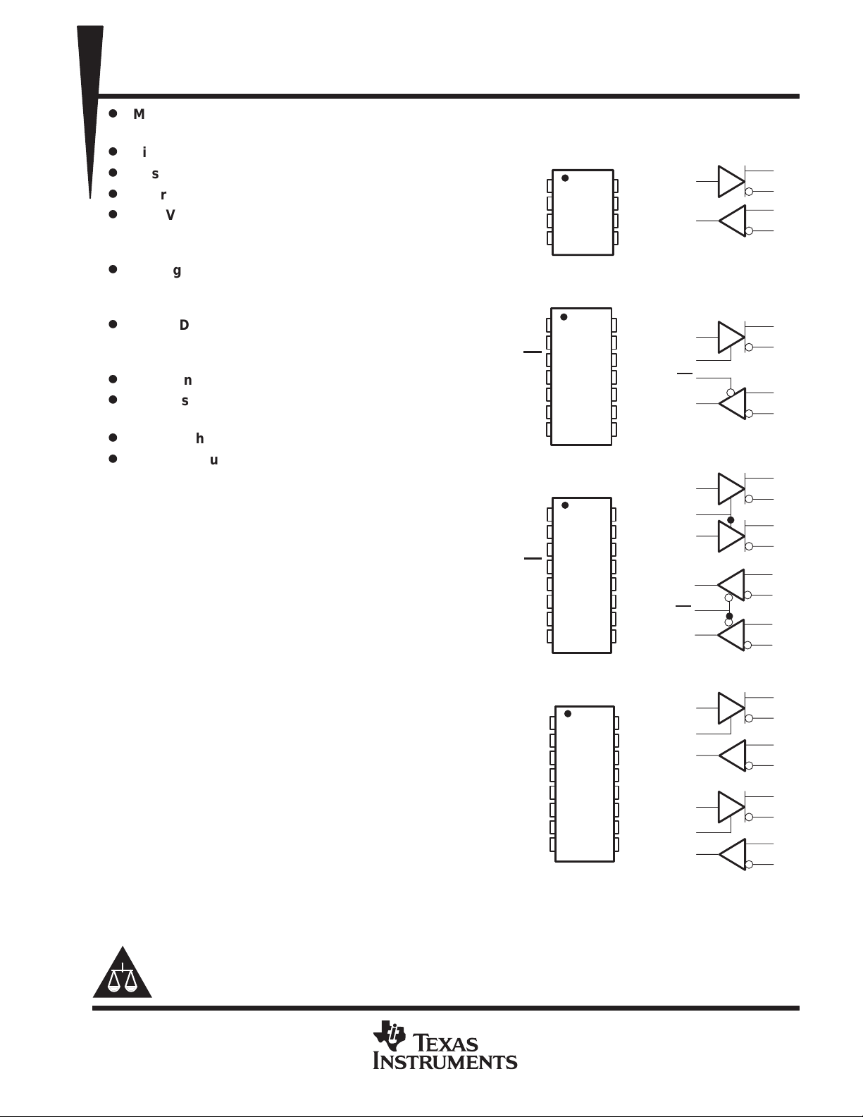
Surface-Mount Packaging
– D Package (SOIC)
– DGK Package (MSOP) (’LVDS79 Only)
description
The SN65LVDS179, SN65LVDS180,
SN65L VDS050, and SN65LVDS051 are dif ferential line drivers and receivers that use low-voltage
differential signaling (LVDS) to achieve signaling
rates as high as 400 Mbps. The TIA/EIA-644
standard compliant electrical interface provides a
minimum differential output voltage magnitude of
247 mV into a 100 Ω load and receipt of 100 mV
signals with up to 1 V of ground potential
difference between a transmitter and receiver.
The intended application of this device and
signaling technique is for point-to-point baseband
data transmission over controlled impedance
media of approximately 100 Ω characteristic
impedance. The transmission media may be
printed-circuit board traces, backplanes, or
cables. (Note: The ultimate rate and distance of
data transfer is dependent upon the attenuation
characteristics of the media, the noise coupling to
the environment, and other application specific
characteristics).
< 1.5 V
CC
SLLS301G – APRIL 1998 – REVISED MARCH 2000
SN65LVDS179D (Marked as DL179 or LVD179)
SN65LVDS179DGK (Marked as S79)
SN65LVDS180D (Marked as LVDS180)
SN65LVDS050D (Marked as LVDS050)
SN65LVDS051D (Marked as LVDS051)
V
CC
GND
NC
RE
DE
GND
GND
1B
1A
1R
RE
2R
2A
2B
GND
1B
1A
1R
1DE
2R
2A
2B
GND
(TOP VIEW)
1
R
2
D
3
4
(TOP VIEW)
1
R
2
3
4
D
5
6
7
(TOP VIEW)
1
2
3
4
5
6
7
8
(TOP VIEW)
1
2
3
4
5
6
7
8
14
13
12
11
10
16
15
14
13
12
11
10
16
15
14
13
12
11
10
A
8
B
7
Z
6
5
Y
V
CC
V
CC
A
B
Z
Y
9
NC
8
V
CC
1D
1Y
D
R
D
DE
RE
R
1D
DE
2D
1Z
DE
1R
2Z
2Y
9
2D
V
CC
1D
1Y
RE
2R
1D
1DE
1R
1Z
2DE
2Z
2Y
9
2D
2D
2DE
2R
15
12
15
12
3
2
5
4
3
2
9
3
4
5
4
3
9
5
5
Y
6
Z
8
A
7
B
9
Y
10
Z
12
A
11
B
14
1Y
13
1Z
10
2Y
11
2Z
2
1A
1
1B
6
2A
7
2B
14
1Y
13
1Z
2
1A
1
1B
10
2Y
11
2Z
6
2A
7
2B
Please be aware that an important notice concerning availability, standard warranty, and use in critical applications of
Texas Instruments semiconductor products and disclaimers thereto appears at the end of this data sheet.
PRODUCTION DATA information is current as of publication date.
Products conform to specifications per the terms of Texas Instruments
standard warranty. Production processing does not necessarily include
testing of all parameters.
POST OFFICE BOX 655303 • DALLAS, TEXAS 75265
Copyright 2000, Texas Instruments Incorporated
1
SN65LVDS179, SN65LVDS180, SN65LVDS050, SN65LVDS051
40°C to 85°C
HIGH-SPEED DIFFERENTIAL LINE DRIVERS AND RECEIVERS
SLLS301G – APRIL 1998 – REVISED MARCH 2000
description (continued)
AVAILABLE OPTIONS
PACKAGE
T
A
°
–
°
The ultimate rate and distance of data transfer is dependent upon the attenuation characteristics
of the media, the noise coupling to the environment, and other application specific characteristics.
The SN65L VDS179, SN65L VDS180, SN65L VDS050, and SN65L VDS051 are characterized for operation from
–40°C to 85°C.
SMALL OUTLINE
(D)
SN65LVDS050D —
SN65LVDS051D —
SN65LVDS179D SN65LVDS179DGK
SN65LVDS180D —
SMALL OUTLINE
(DGK)
NOTE:
Function Tables
SN65LVDS179 RECEIVER
INPUTS
VID = VA – V
VID ≥ 100 mV H
–100 MV < VID < 100 mV ?
VID ≤ –100 mV L
Open H
H = high level, L = low level, ? = indeterminate
SN65LVDS179 DRIVER
INPUT
D Y Z
L L H
H H L
Open L H
H = high level, L = low level
SN65LVDS180, SN65LVDS050, and
SN65LVDS051 RECEIVER
INPUTS
VID = VA – V
VID ≥ 100 mV L H
–100 MV < VID < 100 mV L ?
VID ≤ –100 mV L L
Open L H
X H Z
H = high level, L = low level, Z = high impedance,
X = don’t care
B
OUTPUTS
B
OUTPUT
R
OUTPUT
RE R
2
POST OFFICE BOX 655303 • DALLAS, TEXAS 75265
SN65LVDS179, SN65LVDS180, SN65LVDS050, SN65LVDS051
HIGH-SPEED DIFFERENTIAL LINE DRIVERS AND RECEIVERS
SN65LVDS180, SN65LVDS050, and
SN65LVDS051 DRIVER
INPUTS OUTPUTS
D DE Y Z
L H L H
H H H L
Open H L H
X L Z Z
H = high level, L = low level, Z = high impedance,
X = don’t care
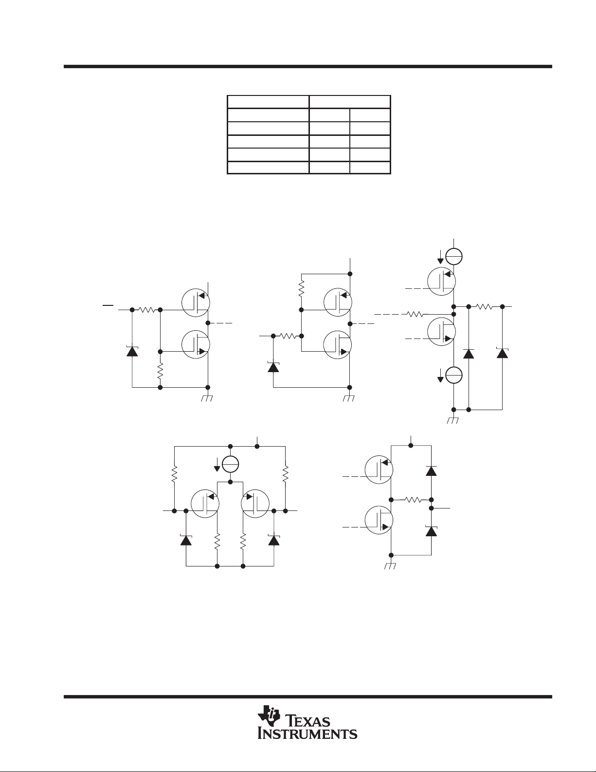
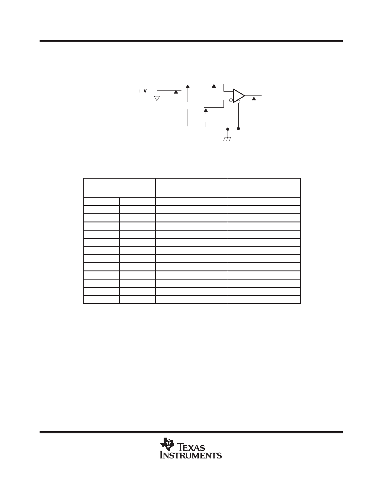
equivalent input and output schematic diagrams
V
CC
300 kΩ
D or RE
Input
7 V
50 Ω
300 kΩ
DE
50 Ω
Input
7 V
SLLS301G – APRIL 1998 – REVISED MARCH 2000
V
CC
V
CC
10 kΩ
5 Ω
Y or Z
Output
7 V
7 V
V
CC
300 kΩ300 kΩ
B InputA Input
7 V
V
CC
5 Ω
R Output
7 V
POST OFFICE BOX 655303 • DALLAS, TEXAS 75265
3
SN65LVDS179, SN65LVDS180, SN65LVDS050, SN65LVDS051
SN65LVDS180
mA
S
current
SN65LVDS050
mA
SN65LVDS051
mA
HIGH-SPEED DIFFERENTIAL LINE DRIVERS AND RECEIVERS
SLLS301G – APRIL 1998 – REVISED MARCH 2000
absolute maximum ratings over operating free-air temperature (unless otherwise noted)
†
Supply voltage range, VCC (see Note 1) –0.5 V to 4 V. . . . . . . . . . . . . . . . . . . . . . . . . . . . . . . . . . . . . . . . . . . . . .
Voltage range (D, R, DE, RE) –0.5 V to 6 V. . . . . . . . . . . . . . . . . . . . . . . . . . . . . . . . . . . . . . . . . . . . . . . . . . . . . . . .
Electrostatic discharge: Y, Z, A, B , and GND (see Note 2) CLass 3, A:12 kV, B:600 V. . . . . . . . . . . . . . . . . .
All Class 3, A:7 kV, B:500 V. . . . . . . . . . . . . . . . . . . . . . . . . . . . . . . . . . . . . . . . . . . . . . . .
Continuous power dissipation see dissipation rating table. . . . . . . . . . . . . . . . . . . . . . . . . . . . . . . . . . . . . . . . . . .
Storage temperature range –65°C to 150°C. . . . . . . . . . . . . . . . . . . . . . . . . . . . . . . . . . . . . . . . . . . . . . . . . . . . . . . .
Lead temperature 1,6 mm (1/16 inch) from case for 10 seconds 250°C. . . . . . . . . . . . . . . . . . . . . . . . . . . . . . .
†
Stresses beyond those listed under “absolute maximum ratings” may cause permanent damage to the device. These are stress ratings only, and
functional operation of the device at these or any other conditions beyond those indicated under “recommended operating conditions” is not
implied. Exposure to absolute-maximum-rated conditions for extended periods may affect device reliability.
NOTES: 1. All voltage values, except differential I/O bus voltages are with respect to network ground terminal.
2. Tested in accordance with MIL-STD-883C Method 3015.7.
DISSIPATION RATING TABLE
PACKAGE
D8 725 mW 5.8 mW/°C 377 mW
D14 or D16 950 mW 7.8 mW/°C 494 mW
DGK 424 mW 3.4 mW/°C 220 mW
†
This is the inverse of the junction-to-ambient thermal resistance when board-mounted and with no air flow.
TA ≤ 25°C
POWER RATING
DERATING FACTOR
ABOVE TA = 25°C
†
TA = 85°C
POWER RATING
recommended operating conditions
MIN NOM MAX UNIT
Supply voltage, V
High-level input voltage, V
Low-level input voltage, V
Magnitude of differential input voltage, VID 0.1 0.6 V
Common–mode input voltage, VIC (see Figure 6)
Operating free–air temperature, T
CC
IH
IL
A
3 3.3 3.6 V
2 V
0.8 V
Ť
Ť
V
ID
2
–40 85 °C
2.4
*
VCC–0.8
Ť
V
ID
2
Ť
V
device electrical characteristics over recommended operating conditions (unless otherwise
noted)
I
†
4
PARAMETER TEST CONDITIONS MIN TYP†MAX UNIT
SN65LVDS179 No receiver load, Driver RL = 100 Ω 9 12 mA
Driver and receiver enabled, No receiver load, Driver RL = 100 Ω 9 12
Driver enabled, Receiver disabled, RL = 100 Ω 5 7
Driver disabled, Receiver enabled, No load 1.5 2
upply
CC
All typical values are at 25°C and with a 3.3-V supply.
Disabled 0.5 1
Drivers and receivers enabled, No receiver loads, Driver RL = 100 Ω 12 20
Drivers enabled, Receivers disabled, RL = 100 Ω 10 16
Drivers disabled, Receivers enabled, No loads 3 6
Disabled 0.5 1
Drivers enabled, No receiver loads, Driver RL = 100 Ω 12 20
Drivers disabled, No loads 3 6
POST OFFICE BOX 655303 • DALLAS, TEXAS 75265
R
100Ω
IIHHigh-level input current
V
V
A
IILLow-level input current
V
V
A
IOSShort-circuit output current
mA
IOZHigh-impedance output current
A
See Figure 5 and Table 1
mV
IIInput current (A or B inputs)
A
SN65LVDS179, SN65LVDS180, SN65LVDS050, SN65LVDS051
HIGH-SPEED DIFFERENTIAL LINE DRIVERS AND RECEIVERS
SLLS301G – APRIL 1998 – REVISED MARCH 2000
driver electrical characteristics over recommended operating conditions (unless otherwise noted)
PARAMETER TEST CONDITIONS MIN TYP MAX UNIT
VOD Differential output voltage magnitude
∆VOD
V
OC(SS)
∆V
OC(SS)
V
OC(PP)
I
O(OFF)
C
IN
Change in differential output voltage magnitude between logic
states
Steady-state common-mode output voltage 1.125 1.2 1.375 V
Change in steady-state common-mode output voltage between
logic states
Peak-to-peak common-mode output voltage 50 150 mV
p
p
p
p
Power-off output current VCC = 0 V, VO = 3.6 V ±1 µA
Input capacitance 3 pF
p
=
L
See Figure 1 and Figure 2
See Figure 3
DE
DE
IH
D
IL
D
VOY or VOZ = 0 V 3 10
VOD = 0 V 3 10
VOD = 600 mV ±1
VO = 0 V or V
,
= 5
= 0.8
CC
247 340 454
±1
mV
µ
µ
µ
–50 50
–50 50 mV
–0.5 –20
2 20
–0.5 –10
2 10
receiver electrical characteristics over recommended operating conditions (unless otherwise
noted)
PARAMETER TEST CONDITIONS MIN TYP†MAX UNIT
V
ITH+
V
ITH–
V
OH
V
OL
I
I(OFF)
I
IH
I
IL
I
OZ
C
I
†
All typical values are at 25°C and with a 3.3-V supply.
Positive-going differential input voltage threshold
Negative-going differential input voltage threshold
High-level output voltage IOH = –8 mA 2.4 V
Low-level output voltage IOL = 8 mA 0.4 V
p
Power-off input current (A or B inputs) VCC = 0 ±20 µA
High-level input current (enables) VIH = 5 V ±10 µA
Low-level input current (enables) VIL = 0.8 V ±10 µA
High-impedance output current VO = 0 or 5 V ±10 µA
Input capacitance 5 pF
p
VI = 0 –2 –11 –20
VI = 2.4 V –1.2 –3
–100
100
µ
POST OFFICE BOX 655303 • DALLAS, TEXAS 75265
5
SN65LVDS179, SN65LVDS180, SN65LVDS050, SN65LVDS051
C
See
6
See Figure 6
See Figure 7
See Figure 7
HIGH-SPEED DIFFERENTIAL LINE DRIVERS AND RECEIVERS
SLLS301G – APRIL 1998 – REVISED MARCH 2000
driver switching characteristics over recommended operating conditions (unless otherwise
noted)
PARAMETER TEST CONDITIONS MIN TYP†MAX UNIT
t
PLH
t
PHL
t
r
t
f
t
sk(p)
t
sk(o)
t
PZH
t
PZL
t
PHZ
t
pLZ
†
All typical values are at 25°C and with a 3.3-V.
‡
t
sk(p)
§
t
sk(o)
¶
t
sk(pp)
operate with the same supply voltages, same temperature, and have identical packages and test circuits.
Propagation delay time, low-to-high-level output 1.7 2.7 ns
Propagation delay time, high-to-low-level output 1.7 2.7 ns
Differential output signal rise time
Differential output signal fall time
Pulse skew (|t
Channel-to-channel output skew
Propagation delay time, high-impedance-to-high-level output 4.3 10 ns
Propagation delay time, high-impedance-to-low-level output
Propagation delay time, high-level-to-high-impedance output
Propagation delay time, low-level-to-high-impedance output 3.4 10 ns
is the magnitude of the time difference between the high-to-low and low-to-high propagation delay times at an output.
is the magnitude of the time difference between the outputs of a single device with all of their inputs connected together.
is the magnitude of the time difference in propagation delay times between any specified terminals of two devices when both devices
pHL
– t
pLH
‡
|)
§
RL = 100Ω,
= 10 pF,
L
Figure
p
0.8 1 ns
0.8 1 ns
300 ps
150 ps
4.6 10 ns
3.1 10 ns
receiver switching characteristics over recommended operating conditions (unless otherwise
noted)
PARAMETER TEST CONDITIONS MIN TYP†MAX UNIT
t
PLH
t
PHL
t
sk(p)
t
r
t
f
t
PZH
t
PZL
t
PHZ
t
PLZ
†
All typical values are at 25°C and with a 3.3-V.
‡
t
sk(p)
§
t
sk(o)
¶
t
sk(pp)
operate with the same supply voltages, same temperature, and have identical packages and test circuits.
Propagation delay time, low-to-high-level output 3.7 4.5 ns
Propagation delay time, high-to-low-level output 3.7 4.5 ns
Pulse skew (|t
Output signal rise time 0.7 1.5 ns
Output signal fall time 0.9 1.5 ns
Propagation delay time, high-level-to-high-impedance output 2.5 ns
Propagation delay time, low-level-to-low-impedance output
Propagation delay time, high-impedance-to-high-level output
Propagation delay time, low-impedance-to-high-level output 4 ns
is the magnitude of the time difference between the high-to-low and low-to-high propagation delay times at an output.
is the magnitude of the time difference between the outputs of a single device with all of their inputs connected together.
is the magnitude of the time difference in propagation delay times between any specified terminals of two devices when both devices
pHL
– t
pLH
‡
|)
CL = 10 pF, See Figure 6
0.3 ns
2.5 ns
7 ns
6
POST OFFICE BOX 655303 • DALLAS, TEXAS 75265

driver
SN65LVDS179, SN65LVDS180, SN65LVDS050, SN65LVDS051
HIGH-SPEED DIFFERENTIAL LINE DRIVERS AND RECEIVERS
PARAMETER MEASUREMENT INFORMATION
I
Driver Enable
I
I
A
V
I
Figure 1. Driver Voltage and Current Definitions
Driver Enable
Input
OY
Y
V
OD
I
OZ
Z
Y
Z
V
OZ
V
OY
V
V
OD
CL = 10 pF
(2 Places)
OC
SLLS301G – APRIL 1998 – REVISED MARCH 2000
VOY)
V
OZ
2
100 Ω
±1%
2 V
Input
t
t
PLH
V
Output
NOTE A: All input pulses are supplied by a generator having the following characteristics: tr or tf ≤ 1 ns, pulse repetition rate (PRR) = 50 Mpps,
pulse width = 10 ± 0.2 ns . CL includes instrumentation and fixture capacitance within 0,06 mm of the D.U.T.
OD(H)
t
f
PHL
V
OD(L)
1.4 V
0.8 V
100%
80%
0 V
20%
0%
t
r
Figure 2. Test Circuit, Timing, and Voltage Definitions for the Differential Output Signal
POST OFFICE BOX 655303 • DALLAS, TEXAS 75265
7

SN65LVDS179, SN65LVDS180, SN65LVDS050, SN65LVDS051
HIGH-SPEED DIFFERENTIAL LINE DRIVERS AND RECEIVERS
SLLS301G – APRIL 1998 – REVISED MARCH 2000
PARAMETER MEASUREMENT INFORMATION
Driver Enable
Y
Input
Z
NOTE A: All input pulses are supplied by a generator having the following characteristics: tr or tf ≤ 1 ns, pulse repetition rate (PRR) = 50 Mpps,
pulse width = 10 ± 0.2 ns . CL includes instrumentation and fixture capacitance within 0,06 mm of the D.U.T . The measurement of V
is made on test equipment with a –3 dB bandwidth of at least 300 MHz.
49.9 Ω, ±1% (2 Places)
CL = 10 pF
(2 Places)
3 V
0 V
V
OC
V
OC
V
OC(PP)
V
OC(SS)
OC(PP)
Figure 3. Test Circuit and Definitions for the Driver Common-Mode Output V oltage
49.9 Ω, ±1% (2 Places)
Y
0.8 V or 2 V
DE
Z
CL = 10 pF
(2 Places)
V
OYVOZ
1.2 V
DE
VOY or V
VOZ or V
NOTE A: All input pulses are supplied by a generator having the following characteristics: tr or tf ≤ 1 ns, pulse repetition rate (PRR) = 0.5 Mpps,
pulse width = 500 ± 10 ns . CL includes instrumentation and fixture capacitance within 0,06 mm of the D.U.T.
OZ
OY
t
PZH
t
PZL
t
PHZ
t
PLZ
2 V
1.4 V
0.8 V
~1.4 V
1.25 V
1.2 V
1.2 V
1.15 V
~1 V
D at 2 V and input to DE
D at 0.8 V and input to DE
Figure 4. Enable and Disable Time Circuit and Definitions
8
POST OFFICE BOX 655303 • DALLAS, TEXAS 75265
receiver
SN65LVDS179, SN65LVDS180, SN65LVDS050, SN65LVDS051
HIGH-SPEED DIFFERENTIAL LINE DRIVERS AND RECEIVERS
SLLS301G – APRIL 1998 – REVISED MARCH 2000
PARAMETER MEASUREMENT INFORMATION
A
VIA)
V
IB
2
V
IA
V
IC
V
ID
B
V
IB
Figure 5. Receiver Voltage Definitions
Table 1. Receiver Minimum and Maximum Input Threshold Test Voltages
R
V
O
APPLIED VOLTAGES
V
1.25 1.15 100 1.2
1.15 1.25 –100 1.2
(V)
IA
2.4 2.3 100 2.35
2.3 2.4 –100 2.35
0.1 0 100 0.05
0 0.1 –100 0.05
1.5 0.9 600 1.2
0.9 1.5 –600 1.2
2.4 1.8 600 2.1
1.8 2.4 –600 2.1
0.6 0 600 0.3
0 0.6 –600 0.3
V
IB
RESULTING DIFFERENTIAL
INPUT VOLTAGE
(mV)
V
ID
RESULTING COMMON-
MODE INPUT VOLTAGE
V
(V)
IC
POST OFFICE BOX 655303 • DALLAS, TEXAS 75265
9

SN65LVDS179, SN65LVDS180, SN65LVDS050, SN65LVDS051
HIGH-SPEED DIFFERENTIAL LINE DRIVERS AND RECEIVERS
SLLS301G – APRIL 1998 – REVISED MARCH 2000
PARAMETER MEASUREMENT INFORMATION
receiver (continued)
V
ID
V
IA
V
IB
C
L
10 pF
V
O
V
IA
V
IB
V
ID
t
PHL
V
O
NOTE A: All input pulses are supplied by a generator having the following characteristics: tr or tf ≤ 1 ns, pulse repetition rate (PRR) = 50 Mpps,
pulse width = 10 ± 0.2 ns. CL includes instrumentation and fixture capacitance within 0,06 m of the D.U.T.
2.4 V
0.4 V
t
f
t
PLH
t
r
1.4 V
1 V
0.4 V
0 V
–0.4 V
V
OH
1.4 V
V
OL
Figure 6. Timing Test Circuit and Waveforms
10
POST OFFICE BOX 655303 • DALLAS, TEXAS 75265

receiver (continued)
SN65LVDS179, SN65LVDS180, SN65LVDS050, SN65LVDS051
HIGH-SPEED DIFFERENTIAL LINE DRIVERS AND RECEIVERS
SLLS301G – APRIL 1998 – REVISED MARCH 2000
PARAMETER MEASUREMENT INFORMATION
1.2 V
Inputs
NOTE A: All input pulses are supplied by a generator having the following characteristics: tr or tf ≤ 1 ns, pulse repetition rate (PRR) = 0.5 Mpps,
pulse width = 500 ± 10 ns. CL includes instrumentation and fixture capacitance within 0,06 m of the D.U.T.
V
TEST
A
RE
t
PZL
RE
t
PZL
B
500 Ω
A
C
L
10 pF
V
O
t
PLZ
+
–
V
2.5 V
1 V
2 V
1.4 V
0.8 V
TEST
2.5 V
1.4 V
V
0 V
1.4 V
2 V
1.4 V
0.8 V
V
1.4 V
0 V
V
TEST
RE
t
R
A
PZH
R
VOL +0.5 V
t
PZH
VOH –0.5 V
t
PHZ
Figure 7. Enable/Disable Time Test Circuit and Waveforms
OL
OH
POST OFFICE BOX 655303 • DALLAS, TEXAS 75265
11

SN65LVDS179, SN65LVDS180, SN65LVDS050, SN65LVDS051
HIGH-SPEED DIFFERENTIAL LINE DRIVERS AND RECEIVERS
SLLS301G – APRIL 1998 – REVISED MARCH 2000
TYPICAL CHARACTERISTICS
COMMON-MODE INPUT VOLTAGE
vs
DIFFERENTIAL INPUT VOLTAGE
2.5
VCC > 3.15 V
4
2
1.5
1
0.5
– Common-Mode Input Voltage – V
IC
V
0
0
DRIVER
LOW-LEVEL OUTPUT VOLTAGE
vs
LOW-LEVEL OUTPUT CURRENT
VCC = 3.3 V
TA = 25°C
VCC = 3 V
MIN
0.1 0.3
0.2 0.4 0.6
|VID|– Differential Input Voltage – V
Figure 8
3.5
VCC = 3.3 V
TA = 25°C
3
0.5
DRIVER
HIGH-LEVEL OUTPUT VOLTAGE
vs
HIGH-LEVEL OUTPUT CURRENT
12
3
2
– Low-Level Output Voltage – V
1
OL
V
0
0
2
IOL – Low-Level Output Current – mA
46
Figure 9
POST OFFICE BOX 655303 • DALLAS, TEXAS 75265
2.5
2
1.5
1
– High-Level Output Voltage – V
OH
0.5
V
0
–4
–3
IOH – High-Level Output Current – mA
–2 0
–1
Figure 10

SN65LVDS179, SN65LVDS180, SN65LVDS050, SN65LVDS051
HIGH-SPEED DIFFERENTIAL LINE DRIVERS AND RECEIVERS
SLLS301G – APRIL 1998 – REVISED MARCH 2000
TYPICAL CHARACTERISTICS
5
4
3
2
– Low-Level Output Votlage – V
1
OL
V
0
RECEIVER
LOW-LEVEL OUTPUT VOLTAGE
vs
LOW-LEVEL OUTPUT CURRENT
VCC = 3.3 V
TA = 25°C
0
10
IOL – Low-Level Output Current – mA
20 30
Figure 11
40 50
60
4
3
2
1
– High-Level Output Voltage – V
OH
V
0
–80
RECEIVER
HIGH-LEVEL OUTPUT VOLTAGE
vs
HIGH-LEVEL OUTPUT CURRENT
VCC = 3.3 V
TA = 25°C
–60
IOH – High-Level Output Current – mA
–40 –20
Figure 12
0
DRIVER
HIGH-TO-LOW LEVEL PROPAGATION DELAY TIME
vs
FREE-AIR TEMPERATURE
2.5
2
PHL – High-To-Low Propagation Delay Time – ns
1.5
t
–50
VCC = 3 V
–30
–10
TA – Free-Air Temperature – °C
VCC = 3.3 V
VCC = 3.6 V
10
30 70
50 90
Figure 13
DRIVER
LOW-TO-HIGH LEVEL PROPAGATION DELAY TIME
vs
FREE-AIR TEMPERATURE
2.5
2
PLH – Low-To-High Propagation Delay Time – ns
1.5
t
–50
VCC = 3 V
–30
–10
TA – Free-Air Temperature – °C
VCC = 3.3 V
VCC = 3.6 V
10
30 70
50 90
Figure 14
POST OFFICE BOX 655303 • DALLAS, TEXAS 75265
13

SN65LVDS179, SN65LVDS180, SN65LVDS050, SN65LVDS051
HIGH-SPEED DIFFERENTIAL LINE DRIVERS AND RECEIVERS
SLLS301G – APRIL 1998 – REVISED MARCH 2000
TYPICAL CHARACTERISTICS
RECEIVER
HIGH-TO-LOW LEVEL PROPAGATION DELAY TIME
vs
FREE-AIR TEMPERATURE
4.5
4
3.5
– High-To-Low Level Propagation Dealy T ime – ns
2.5
PLH
t
3
–50
VCC = 3 V
–30
TA – Free–Air Temperature – °C
VCC = 3.3 V
VCC = 3.6 V
–10
10
50 90
30 70
Figure 15
RECEIVER
LOW-TO-HIGH LEVEL PROPAGATION DELAY TIME
vs
FREE–AIR TEMPERATURE
4.5
VCC = 3 V
4
3.5
3
2.5
PLH – Low-To-High Level Propagation Delay Time – ns
t
–50
–30
VCC = 3.3 V
VCC = 3.6 V
–10
TA – Free-Air Temperature – °C
10
50 90
30 70
Figure 16
14
POST OFFICE BOX 655303 • DALLAS, TEXAS 75265

SN65LVDS179, SN65LVDS180, SN65LVDS050, SN65LVDS051
HIGH-SPEED DIFFERENTIAL LINE DRIVERS AND RECEIVERS
SLLS301G – APRIL 1998 – REVISED MARCH 2000
APPLICATION INFORMATION
The devices are generally used as building blocks for high-speed point-to-point data transmission. Ground
differences are less than 1 V with a low common–mode output and balanced interface for very low noise emissions.
Devices can interoperate with RS-422, PECL, and IEEE-P1596. Drivers/Receivers maintain ECL speeds without the
power and dual supply requirements.
1000
100
5% Jitter
10
1
Transmission Distance – m
24 AWG UTP 96 Ω (PVC Dielectric)
0.1
100k 10M 100M
1M
30% Jitter
Data Rate – Hz
Figure 17. Data Transmission Distance Versus Rate
POST OFFICE BOX 655303 • DALLAS, TEXAS 75265
15
SN65LVDS179, SN65LVDS180, SN65LVDS050, SN65LVDS051
HIGH-SPEED DIFFERENTIAL LINE DRIVERS AND RECEIVERS
SLLS301G – APRIL 1998 – REVISED MARCH 2000
APPLICATION INFORMATION
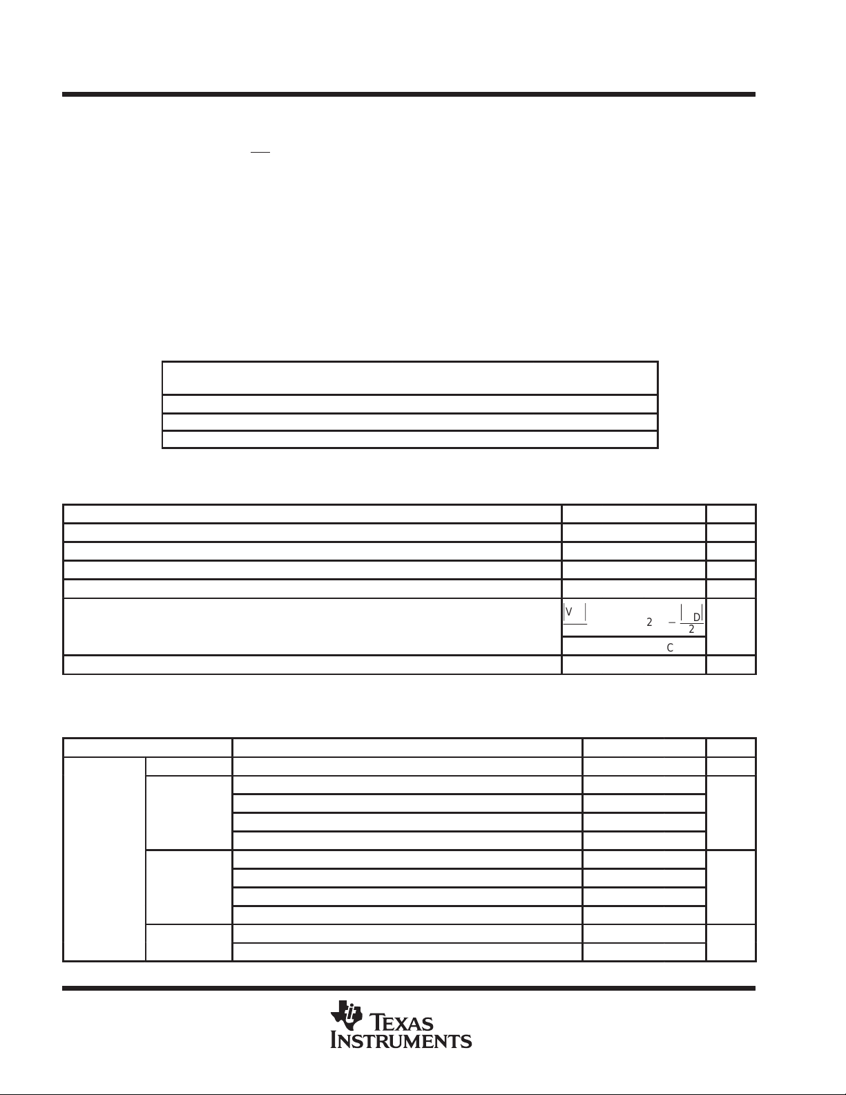
fail safe
One of the most common problems with differential signaling applications is how the system responds when
no differential voltage is present on the signal pair . The LVDS receiver is like most differential line receivers, in
that its output logic state can be indeterminate when the differential input voltage is between –100 mV and
100 mV and within its recommended input common-mode voltage range. TI’s L VDS receiver is different in how
it handles the open-input circuit situation, however.
Open-circuit means that there is little or no input current to the receiver from the data line itself. This could be
when the driver is in a high-impedance state or the cable is disconnected. When this occurs, the L VDS receiver
will pull each line of the signal pair to near V
feature uses an AND gate with input voltage thresholds at about 2.3 V to detect this condition and force the
output to a high-level regardless of the differential input voltage.
300 kΩ 300 kΩ
through 300-kΩ resistors as shown in Figure 1 1. The fail-safe
CC
V
CC
A
R
100 Ω Typ
t
Y
B
VIT ≈ 2.3 V
Figure 18. Open-Circuit Fail Safe of the LVDS Receiver
It is only under these conditions that the output of the receiver will be valid with less than a 100-mV differential
input voltage magnitude. The presence of the termination resistor, Rt, does not af fect the fail-safe function as
long as it is connected as shown in the figure. Other termination circuits may allow a dc current to ground that
could defeat the pullup currents from the receiver and the fail-safe feature.
16
POST OFFICE BOX 655303 • DALLAS, TEXAS 75265

SN65LVDS179, SN65LVDS180, SN65LVDS050, SN65LVDS051
HIGH-SPEED DIFFERENTIAL LINE DRIVERS AND RECEIVERS
SLLS301G – APRIL 1998 – REVISED MARCH 2000
MECHANICAL DATA
D (R-PDSO-G**) PLASTIC SMALL-OUTLINE PACKAGE
14 PIN SHOWN
0.050 (1,27)
14
1
0.069 (1,75) MAX
0.020 (0,51)
0.014 (0,35)
8
7
A
0.010 (0,25)
0.004 (0,10)
DIM
0.157 (4,00)
0.150 (3,81)
PINS **
0.010 (0,25)
0.244 (6,20)
0.228 (5,80)
8
M
Seating Plane
0.004 (0,10)
14
0.008 (0,20) NOM
0°–8°
16
Gage Plane
0.010 (0,25)
0.044 (1,12)
0.016 (0,40)
A MAX
A MIN
NOTES: A. All linear dimensions are in inches (millimeters).
B. This drawing is subject to change without notice.
C. Body dimensions do not include mold flash or protrusion, not to exceed 0.006 (0,15).
D. Falls within JEDEC MS-012
POST OFFICE BOX 655303 • DALLAS, TEXAS 75265
0.197
(5,00)
0.189
(4,80)
0.344
(8,75)
0.337
(8,55)
0.394
(10,00)
0.386
(9,80)
4040047/D 10/96
17

SN65LVDS179, SN65LVDS180, SN65LVDS050, SN65LVDS051
HIGH-SPEED DIFFERENTIAL LINE DRIVERS AND RECEIVERS
SLLS301G – APRIL 1998 – REVISED MARCH 2000
MECHANICAL DATA
DGK (R-PDSO-G8) PLASTIC SMALL-OUTLINE PACKAGE
0,65
0,38
0,25
8
1
3,05
2,95
5
3,05
2,95
4
Seating Plane
0,25
4,98
4,78
M
0,15 NOM
Gage Plane
0,25
0°–6°
0,69
0,41
1,07 MAX
NOTES: A. All linear dimensions are in millimeters.
B. This drawing is subject to change without notice.
C. Body dimensions do not include mold flash or protrusion.
D. Falls within JEDEC MO-187
0,15 MIN
0,10
4073329/A 02/97
18
POST OFFICE BOX 655303 • DALLAS, TEXAS 75265

IMPORTANT NOTICE
T exas Instruments and its subsidiaries (TI) reserve the right to make changes to their products or to discontinue
any product or service without notice, and advise customers to obtain the latest version of relevant information
to verify, before placing orders, that information being relied on is current and complete. All products are sold
subject to the terms and conditions of sale supplied at the time of order acknowledgement, including those
pertaining to warranty, patent infringement, and limitation of liability.
TI warrants performance of its semiconductor products to the specifications applicable at the time of sale in
accordance with TI’s standard warranty. Testing and other quality control techniques are utilized to the extent
TI deems necessary to support this warranty . Specific testing of all parameters of each device is not necessarily
performed, except those mandated by government requirements.
CERTAIN APPLICA TIONS USING SEMICONDUCTOR PRODUCTS MA Y INVOLVE POTENTIAL RISKS OF
DEATH, PERSONAL INJURY, OR SEVERE PROPERTY OR ENVIRONMENTAL DAMAGE (“CRITICAL
APPLICATIONS”). TI SEMICONDUCTOR PRODUCTS ARE NOT DESIGNED, AUTHORIZED, OR
WARRANTED TO BE SUITABLE FOR USE IN LIFE-SUPPORT DEVICES OR SYSTEMS OR OTHER
CRITICAL APPLICA TIONS. INCLUSION OF TI PRODUCTS IN SUCH APPLICATIONS IS UNDERST OOD TO
BE FULLY AT THE CUSTOMER’S RISK.
In order to minimize risks associated with the customer’s applications, adequate design and operating
safeguards must be provided by the customer to minimize inherent or procedural hazards.
TI assumes no liability for applications assistance or customer product design. TI does not warrant or represent
that any license, either express or implied, is granted under any patent right, copyright, mask work right, or other
intellectual property right of TI covering or relating to any combination, machine, or process in which such
semiconductor products or services might be or are used. TI’s publication of information regarding any third
party’s products or services does not constitute TI’s approval, warranty or endorsement thereof.
Copyright 2000, Texas Instruments Incorporated
 Loading...