

Page 1
User’s Guide
SWRU321A – May 2013
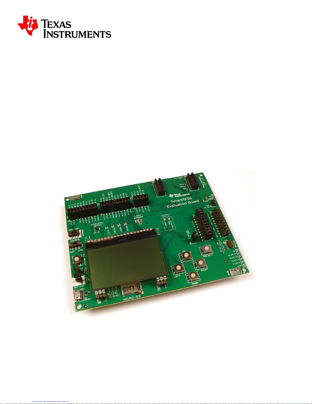
SmartRF06 Evaluation Board
User’s Guide
SmartRF™ is a trademark of Texas Instruments
Page 2

Page 3

User’s Guide
SWRU321A – May 2013
Table of Contents
4.1 INSTALLING SMARTRF STUDIO AND USB DRIVERS ................................................................ 7
4.1.1 SmartRF Studio ................................................................................................................. 7
4.1.2 FTDI USB driver ................................................................................................................ 7
5.1 ABSOLUTE MAXIMUM RATINGS ........................................................................................... 11
6.1 XDS100V3 EMULATOR ...................................................................................................... 13
6.1.1 UART back channel ........................................................................................................ 14
6.2 POWER SOURCES ............................................................................................................. 14
6.2.1 USB Power ...................................................................................................................... 15
6.2.2 Battery Power .................................................................................................................. 15
6.2.3 External Power Supply .................................................................................................... 16
6.3 POWER DOMAINS .............................................................................................................. 17
6.3.1 XDS Domain ................................................................................................................... 17
6.3.2 EM Domain...................................................................................................................... 17
6.3.3 3.3 V Domain .................................................................................................................. 18
6.4 LCD ................................................................................................................................. 18
6.5 MICRO SD CARD SLOT ...................................................................................................... 19
6.6 ACCELEROMETER .............................................................................................................. 19
6.7 AMBIENT LIGHT SENSOR .................................................................................................... 20
6.8 BUTTONS .......................................................................................................................... 20
6.9 LEDS ............................................................................................................................... 21
6.9.1 General Purpose LEDs ................................................................................................... 21
6.9.2 XDS100v3 Emulator LEDs .............................................................................................. 21
6.10 EM CONNECTORS ............................................................................................................. 21
6.11 BREAKOUT HEADERS AND JUMPERS ................................................................................... 23
6.11.1 I/O Breakout Headers ..................................................................................................... 23
6.11.2 XDS100v3 Emulator Bypass Headers ............................................................................ 24
6.11.3 20-pin ARM JTAG Header .............................................................................................. 25
6.11.4 10-pin ARM Cortex Debug Header ................................................................................. 26
6.12 CURRENT MEASUREMENT .................................................................................................. 27
6.12.1 High-side current sensing ............................................................................................... 27
6.12.2 Current Measurement Jumper ........................................................................................ 27
7.1 20-PIN ARM JTAG HEADER .............................................................................................. 29
7.2 10-PIN ARM CORTEX DEBUG HEADER ............................................................................... 29
7.3 CUSTOM STRAPPING ......................................................................................................... 30
List of Figures
Figure 1 – Driver install: a) Update driver, b) Specify path to FTDI drivers..................................... 8
Figure 2 – Driver install: a) VCP loaded and b) drivers successfully installed ................................ 8
Figure 3 – SmartRF06EB (rev. 1.2.1) with EM connected ............................................................ 10
Figure 4 – SmartRF06EB architecture .......................................................................................... 12
Figure 5 – SmartRF06EB revision 1.2.1 front side ........................................................................ 13
Figure 6 – SmartRF06EB revision 1.2.1 reverse side ................................................................... 13
Figure 7 – Jumper mounted on J5 to enable the UART back channel ......................................... 14
Figure 8 – Main power switch (P501) and source selection switch (P502) ................................... 15
Figure 9 – SmartRF06EB power selection switch (P502) in “USB” position ................................. 15
Figure 10 – SmartRF06EB power source selection switch (P502) in “BAT” position ................... 16
Figure 11 – SmartRF06EB external power supply header (J501) ................................................ 16
Figure 12 – Power domain overview of SmartRF06EB ................................................................. 17
Figure 13 – Mount a jumper on J502 to bypass EM domain voltage regulator ............................. 18
Figure 14 – Simplified schematic of Ambient Light Sensor setup ................................................. 20
Figure 15 – SmartRF06EB EM connectors RF1 and RF2 ............................................................ 21
Page 3/32
Page 4

User’s Guide
SWRU321A – May 2013
Figure 16 – SmartRF06EB I/O breakout overview ........................................................................ 23
Figure 17 – XDS100v3 Emulator Bypass Header (P408) ............................................................. 24
Figure 18 – 20-pin ARM JTAG header (P409) .............................................................................. 25
Figure 19 – 10-pin ARM Cortex Debug header (P410) ................................................................. 26
Figure 20 – Simplified schematic of high-side current sensing setup ........................................... 27
Figure 21 – Measuring current consumption using jumper J503 .................................................. 27
Figure 22 – Simplified connection diagram for different debugging scenarios ............................. 28
Figure 23 – Debugging external target using SmartRF06EB ........................................................ 29
Figure 24 – ARM JTAG header (P409) with strapping to debug external target .......................... 30
List of Tables
Table 1 – SmartRF06EB features ................................................................................................... 5
Table 2 – Supply voltage: Recommended operating conditions and absolute max. ratings ........ 11
Table 3 – Temperature: Recommended operating conditions and storage temperatures ........... 11
Table 4 – UART Back channel signal connections ....................................................................... 14
Table 5 – Power domain overview of SmartRF06EB .................................................................... 17
Table 6 – LCD signal connections ................................................................................................. 19
Table 7 – Micro SD Card signal connections ................................................................................ 19
Table 8 – Accelerometer signal connections ................................................................................. 20
Table 9 – Ambient Light Sensor signal connections ..................................................................... 20
Table 10 – Button signal connections ........................................................................................... 20
Table 11 – General purpose LED signal connections ................................................................... 21
Table 12 – EM connector RF1 pin-out........................................................................................... 22
Table 13 – EM connector RF2 pin-out........................................................................................... 22
Table 14 – SmartRF06EB I/O breakout overview ......................................................................... 24
Table 15 – 20-pin ARM JTAG header pin-out (P409) ................................................................... 25
Table 16 – 10-pin ARM Cortex Debug header pin-out (P410) ...................................................... 26
Table 17 – Debugging external target: Minimum strapping (cJTAG support) ............................... 30
Table 18 – Debugging external target: Optional strapping ............................................................ 30
Page 4/32
Page 5
User’s Guide
Component
Description
TI XDS100v3 Emulator
cJTAG and JTAG emulator for easy programming and
debugging of SoCs on Evaluation Modules or external targets.
High-speed USB 2.0
interface
Easy plug and play access to full SoC control using SmartRF™
Studio PC software. Integrated serial port over USB enables
communication between the SoC via the UART back channel.
64x128 pixels serial LCD
Big LCD display for demo use and user interface development.
LEDs
Four general purpose LEDs for demo use or debugging.
Micro SD card slot
External flash for extra storage, over-the-air upgrades and more.
Buttons
Five push-buttons for demo use and user interfacing.
Accelerometer
Three-axis highly configurable digital accelerometer for
application development and demo use.
Light Sensor
Ambient Light Sensor for application development and demo
use.
Current measurement
Current sense amplifier for high side current measurements.
Breakout pins
Easy access to SoC GPIO pins for quick and easy debugging.
SWRU321A – May 2013
1 Introduction
The SmartRF06 Evaluation Board (SmartRF06EB or simply EB) is the motherboard in
development kits for Low Power RF ARM Cortex®-M based System on Chips from Texas
Instruments. The board has a wide range of features, listed in Table 1 below.
Table 1 – SmartRF06EB features
2 About this manual
This manual contains reference information about the SmartRF06EB.
Chapter 4 will give a quick introduction on how to get started with the SmartRF06EB. It describes
how to install SmartRF™ Studio to get the required USB drivers for the evaluation board. Chapter
5 briefly explains how the EB can be used throughout a project’s development cycle. Chapter 6
gives an overview of the various features and functionality provided by the board.
A troubleshooting guide is found in chapter 8 and Appendix A contains the schematics for
SmartRF06EB revision 1.2.1.
The PC tools SmartRF™ Studio and SmartRF™ Flash Programmer have their own user manual.
See chapter 9 for references to relevant documents and web pages.
Page 5/32
Page 6

User’s Guide
SWRU321A – May 2013
3 Acronyms and Abbreviations
ALS Ambient Light Sensor
cJTAG Compact JTAG (IEEE 1149.7)
CW Continuous Wave
DK Development Kit
EB Evaluation Board
EM Evaluation Module
FPGA Field-Programmable Gate Array
I/O Input/Output
JTAG Joint Test Action Group (IEEE 1149.1)
LCD Liquid Crystal Display
LED Light Emitting Diode
LPRF Low Power RF
MCU Micro Controller
MISO Master In, Slave Out (SPI signal)
MOSI Master Out, Slave In (SPI signal)
NA Not Applicable / Not Available
NC Not Connected
RF Radio Frequency
RTS Request to Send
RX Receive
SoC System on Chip
SPI Serial Peripheral Interface
TI Texas Instruments
TP Test Point
TX Transmit
UART Universal Asynchronous Receive Transmit
USB Universal Serial Bus
VCP Virtual COM Port
Page 6/32
Page 7

User’s Guide
SWRU321A – May 2013
4 Getting Started
Before connecting the SmartRF06EB to the PC via the USB cable, it is highly recommended to
perform the steps described below.
4.1 Installing SmartRF Studio and USB drivers
Before your PC can communicate with the SmartRF06EB over USB, you will need to install the
USB drivers for the EB. The latest SmartRF Studio installer [1] includes USB drivers both for
Windows x86 and Windows x64 platforms.
After you have downloaded SmartRF Studio from the web, extract the zip-file, run the installer
and follow the instructions. Select the complete installation to include the SmartRF Studio
program, the SmartRF Studio documentation and the necessary drivers needed to communicate
with the SmartRF06EB.
4.1.1 SmartRF Studio
SmartRF Studio is a PC application developed for configuration and evaluation of many RF-IC
products from Texas Instruments. The application is designed for use with SmartRF Evaluation
Boards, such as SmartRF06EB, and runs on Microsoft Windows operating systems.
SmartRF Studio lets you explore and experiment with the RF-ICs as it gives full overview and
access to the devices’ registers to configure the radio and has a control interface for simple radio
operation from the PC.
This means that SmartRF Studio will help radio system designers to easily evaluate the RF-IC at
an early stage in the design process. It also offers a flexible code export function of radio register
settings for software developers.
The latest version of SmartRF Studio can be downloaded from the Texas Instruments website [1],
where you will also find a complete user manual.
4.1.2 FTDI USB driver
SmartRF PC software such as SmartRF Studio uses a proprietary USB driver from FTDI [2] to
communicate with SmartRF06 evaluation boards. Connect your SmartRF06EB to the computer
with a USB cable and turn it on. If you did a complete install of SmartRF Studio, Windows will
recognize the device automatically and the SmartRF06EB is ready for use!
4.1.2.1 Install FTDI USB driver manually in Windows
If the SmartRF06EB was not properly recognized after plugging it into your PC, try the following
steps to install the necessary USB drivers. The steps described are for Microsoft Windows 7, but
are very similar to those in Windows XP and Windows Vista. It is assumed that you have already
downloaded and installed the latest version of SmartRF Studio 7 [1].
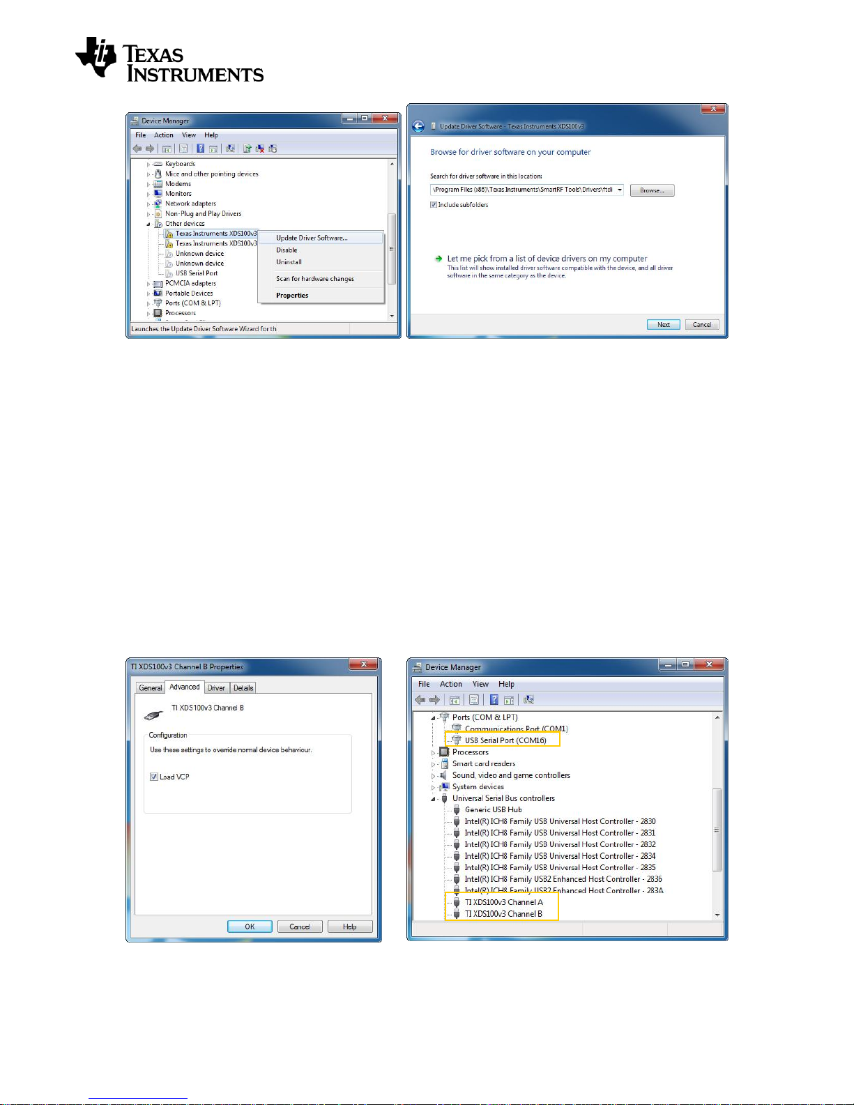
Open the Windows Device Manager and right click on the first “Texas Instruments XDS100v3”
found under “Other devices” as shown in Figure 1a.
Select “Update Driver Software…” and, in the appearing dialog, browse to
<Studio install dir>\Drivers\ftdi as shown in Figure 1b.
Page 7/32
Page 8
User’s Guide
a) b)
SWRU321A – May 2013
Figure 1 – Driver install: a) Update driver, b) Specify path to FTDI drivers
Press Next and wait for the driver to be installed. The selected device should now appear in the
Device Manager as “TI XDS100v3 Channel x” (x = A or B) as seen in Figure 2b. Repeat the
above steps for the second “Texas Instruments XDS100v3” listed under “Other devices”.
4.1.2.1.1 Enable XDS100v3 UART back channel on Windows
If you have both “TI XDS100v3 Channel A” and “TI XDS100v3 Channel B” listed under Universal
Serial Bus Controllers, you can proceed. Right click on “TI XDS100v3 Channel B” and select
Properties. Under the Advanced tab, make sure “Load VCP” is checked as shown in Figure 2a.
A “USB Serial Port” may be listed under “Other devices”, as seen in Figure 1a. Follow the same
steps as for the “Texas Instruments XDS100v3” devices to install the VCP driver. When the
drivers from <Studio install dir>\Drivers\ftdi is properly installed, you should see the USB Serial
Port device be listed under “Ports (COM & LPT)” as shown in Figure 2b.
The SmartRF06EB drivers are now installed correctly.
Figure 2 – Driver install: a) VCP loaded and b) drivers successfully installed
Page 8/32
Page 9

User’s Guide
SWRU321A – May 2013
4.1.2.2 Install XSD100v3 UART back channel on Linux
The ports on SmartRF06EB will typically be mounted as ttyUSB0 or ttyUSB1. The UART back
channel is normally mounted as ttyUSB1.
1. Download the Linux drivers from [2].
2. Untar the ftdi_sio.tar.gz file on your Linux system.
3. Connect the SmartRF06EB to your system.
4. Install driver
a. Verify the USB Product ID (PID) and Vendor ID (VID).
The TI XDS100v3 USB VID is 0x0403 and the PID is 0xA6D1, but if you wish to
find the PID using a terminal window/shell, use
> lsusb | grep -i future
b. Install driver using modprobe
In a terminal window/shell, navigate to the ftdi_sio folder and run
> sudo modprobe ftdi_sio vendor=0x403 product=0xA6D1
SmartRF06EB should now be correctly mounted. The above steps have been tested on Fedora
and Ubuntu distributions.
If the above steps failed, try uninstalling ‘brltty’ prior to step 5 (technical note TN_101, [2]).
> sudo apt-get remove brltty
Page 9/32
Page 10
User’s Guide
SWRU321A – May 2013
5 Using the SmartRF06 Evaluation Board
The SmartRF06EB is a flexible test and development platform that works together with RF
Evaluation Modules from Texas Instruments.
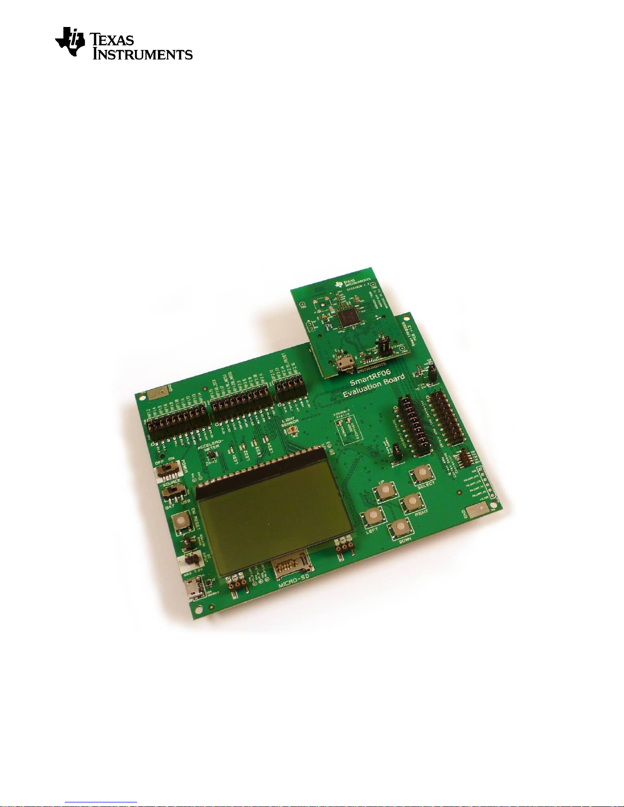
An Evaluation Module (EM) is a small RF module with RF chip, balun, matching filter, SMA
antenna connector and I/O connectors. The modules can be plugged into the SmartRF06EB
which lets the PC take direct control of the RF device on the EM over the USB interface.
SmartRF06EB currently supports:
- CC2538EM
SmartRF06EB is included in e.g. the CC2538 development kit.
Figure 3 – SmartRF06EB (rev. 1.2.1) with EM connected
The PC software that controls the SmartRF06EB + EM is SmartRF Studio. Studio can be used to
perform several RF tests and measurements, e.g. to set up a CW signal and send/receive
packets.
Page 10/32
Page 11
User’s Guide
Component
Operating voltage
Absolute max. rating
Min. [V]
Max. [V]
Min. [V]
Max. [V]
XDS100v3 Emulator1 [4]
+1.8
+3.6
-0.3
+3.75
LCD [5]
+3.0
+3.3
-0.3
+3.6
Accelerometer [6]
+1.62
+3.6
-0.3
+4.25
Ambient light sensor [7]
+2.32
+5.5
NA
+6
Component
Operating temperature
Storage temperature
Min. [˚C]
Max. [˚C]
Min. [˚C]
Max. [˚C]
XDS100v3 Emulator [4]
-20
+70
-50
+110
LCD [5]
-20
+70
-30
+80
Accelerometer [6]
-40
+85
-50
+150
Ambient light sensor [7]
-40
+85
-40
+85
1
2
SWRU321A – May 2013
The EB+EM can be of great help during the whole development cycle for a new RF product.
- Perform comparative studies. Compare results obtained with EB+EM with results from
your own system.
- Perform basic functional tests of your own hardware by connecting the radio on your
board to SmartRF06EB. SmartRF Studio can be used to exercise the radio.
- Verify your own software with known good RF hardware, by simply connecting your own
microcontroller to an EM via the EB. Test the send function by transmitting packets from
your SW and receive with another board using SmartRF Studio. Then transmit using
SmartRF Studio and receive with your own software.
- Develop code for your SoC and use the SmartRF06EB as a standalone board without PC
tools.
The SmartRF06EB can also be used as a debugger interface to the SoCs from IAR Embedded
workbench for ARM or Code Composer Studio from Texas Instruments. For details on how to use
the SmartRF06EB to debug external targets, see chapter 7.
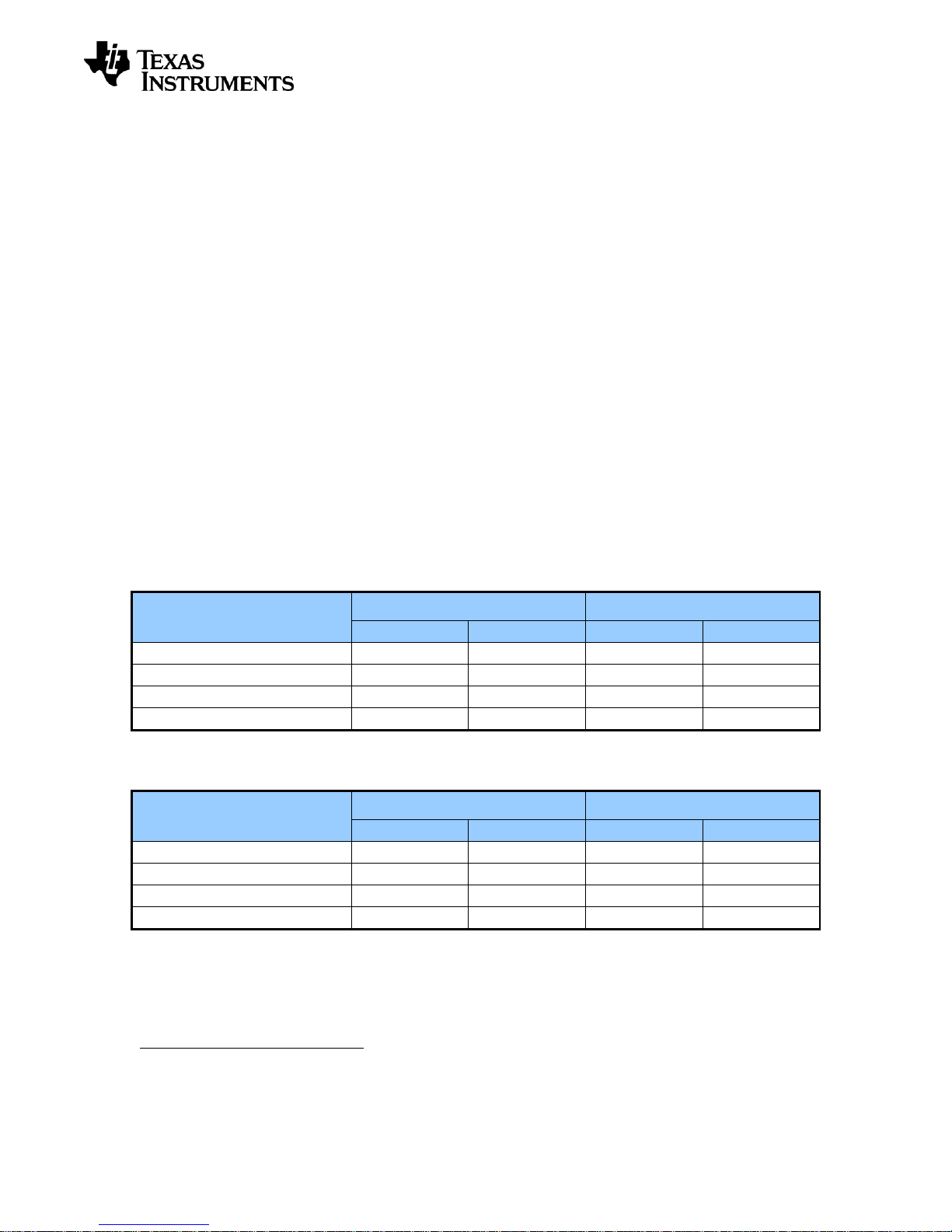
5.1 Absolute Maximum Ratings
The minimum and maximum operating supply voltages and absolute maximum ratings for the
active components onboard the SmartRF06EB are summarized in Table 2. Table 3 lists the
recommended operating temperature and storage temperature ratings. Please refer to the
respective component’s datasheet for further details.
Table 2 – Supply voltage: Recommended operating conditions and absolute max. ratings
Table 3 – Temperature: Recommended operating conditions and storage temperatures
The XDS100v3 Emulator is USB powered. Values refer to the supply and I/O pin voltages of the connected target.
Recommended minimum operating voltage.
Page 11/32
Page 12
User’s Guide
EM Domain (1.8 – 3.6 V)
XDS Domain
3.3 V Domain
EM Connectors
AccelerometerLEDsButtonsLight Sensor
XDS100v3
Emulator
XDS
LEDs
Level shifter
SD Card Reader
Load switch
20-pin
ARM JTAG
Header
Bypass Header
UART back
channel
Level shifter
10-pin
ARM Cortex
Debug Header
(c)JTAG
USB
I/O breakout headers
3.3 V Domain
Enable
LCD
I/O Breakout Headers
SWRU321A – May 2013
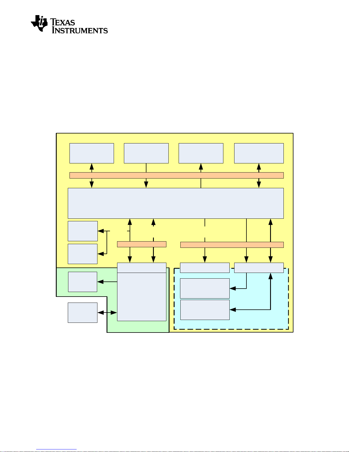
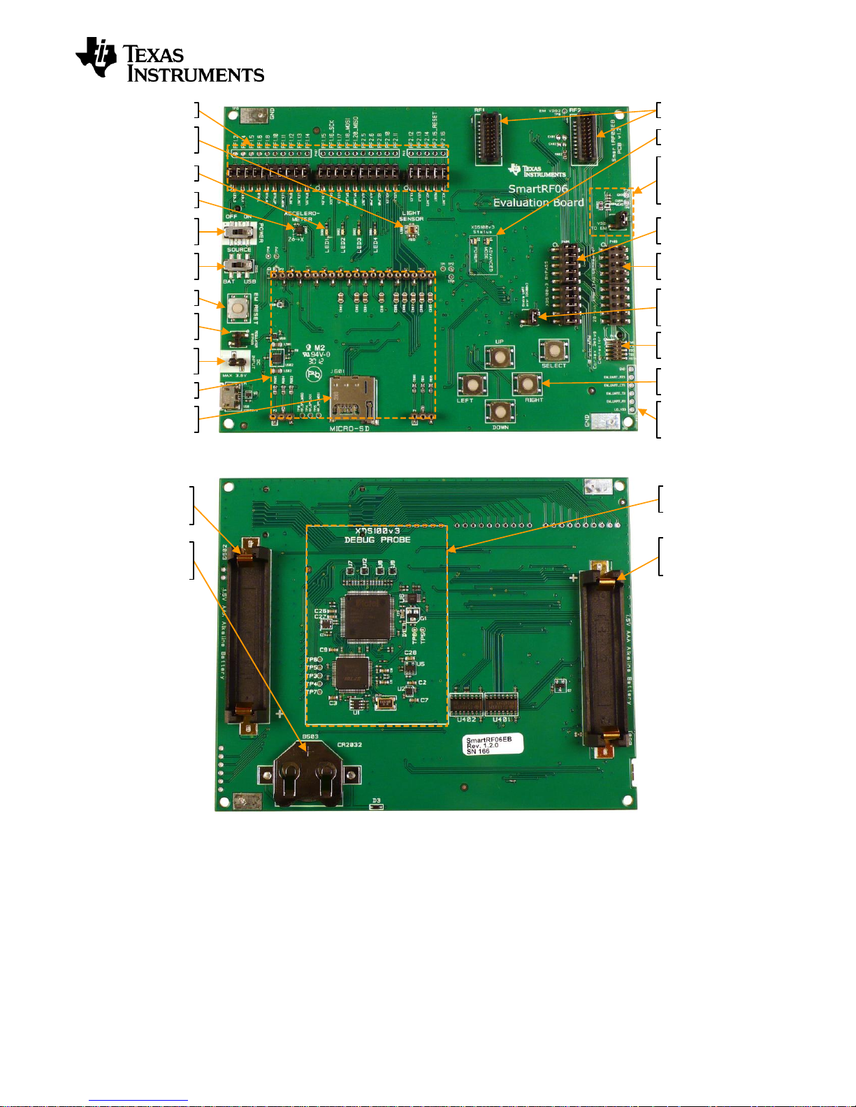
6 SmartRF06 Evaluation Board Overview
SmartRF06EB acts as the motherboard in development kits for ARM® Cortex™ based Low
Power RF SoCs from Texas Instruments. The board has several user interfaces and connections
to external interfaces, allowing fast prototyping and testing of both software and hardware. An
overview of the SmartRF06EB architecture is found in Figure 4. The board layout is found in
Figure 5 and Figure 6, while the schematics are located in Appendix A.
This chapter will give an overview of the general architecture of the board and describe the
available I/O. The following sub-sections will explain the I/O in more detail. Pin connections
between the EM and the evaluation board I/O can be found in section 6.10.
Figure 4 – SmartRF06EB architecture
Page 12/32
Page 13
User’s Guide
EM current
measurement
testpoint and
jumper
XDS bypass
header
20-pin ARM
JTAG Header
General purpose
buttons
UART back
channel
breakout
XDS LEDs
10-pin ARM
Cortex Header
EM I/O breakout
Main power
switch
Power source
selection switch
External power
supply connector
EM reset button
Regulator
bypass jumper
Micro SD
card slot
LCD
Accelerometer
LEDs
Ambient Light
Sensor
EM connectors
UART back
channel enable
Jumper
1.5 V AAA
Alkaline Battery
holder
XDS100v3
Emulator
1.5 V AAA
Alkaline Battery
holder
CR2032 coin
cell battery
holder
SWRU321A – May 2013
Figure 5 – SmartRF06EB revision 1.2.1 front side
Figure 6 – SmartRF06EB revision 1.2.1 reverse side
6.1 XDS100v3 Emulator
The XDS100v3 Emulator from Texas Instruments has cJTAG and regular JTAG support. cJTAG
is a 2-pin extension to regular 4-pin JTAG. The XDS100v3 consists of a USB to JTAG chip from
FTDI [2] and an FPGA to convert JTAG instructions to cJTAG format.
Page 13/32
Page 14
User’s Guide
Signal name
Description
Probe header
EM pin
RF1.7_UART_RX
UART Receive (EM data in)
EM_UART_RX (P412.2)
RF1.7
RF1.9_UART_TX
UART Transmit (EM data out)
EM_UART_TX (P412.3)
RF1.9
RF1.3_UART_CTS
UART Clear To Send signal
EM_UART_CTS (P412.4)
RF1.3
RF2.18_UART_RTS
UART Request To Send signal
EM_UART_RTS (P412.5)
RF2.18
Never connect batteries and an external power source to the SmartRF06EB at the
same time! Doing so may lead to excessive currents that may damage the batteries
or cause onboard components to break. The CR2032 coin cell battery is in particular
very sensitive to reverse currents (charging) and must never be combined with other
power sources (AAA batteries or an external power source).
SWRU321A – May 2013
In addition to regular debugging capabilities using cJTAG or JTAG, the XDS100v3 Emulator
supports a UART backchannel over a USB Virtual COM Port (VCP) to the PC. The UART back
channel supports flow control, 8-N-1 format and data rates up to 12Mbaud.
Please see the XDS100v3 emulator product page [4] for detailed information about the emulator.
The XDS100v3 Emulator is powered over USB and is switched on as long as the USB cable is
connected to the SmartRF06EB and the main power switch (S501) is in the ON position. The
XDS100v3 Emulator supports targets with operating voltages between 1.8 V and 3.6. The min
(max) operating temperature is -20 (+70) ˚C.
6.1.1 UART back channel
The mounted EM can be connected to the PC via the XDS100v3 Emulator’s UART back channel.
When connected to a PC, the XDS100v3 is enumerated as a Virtual COM Port (VCP) over USB.
The driver used is a royalty free VCP driver from FTDI, available for e.g. Microsoft Windows,
Linux and Max OS X. The UART back channel gives the mounted EM access to a four pin UART
interface, supporting 8-N-1 format at data rates up to 12 Mbaud.
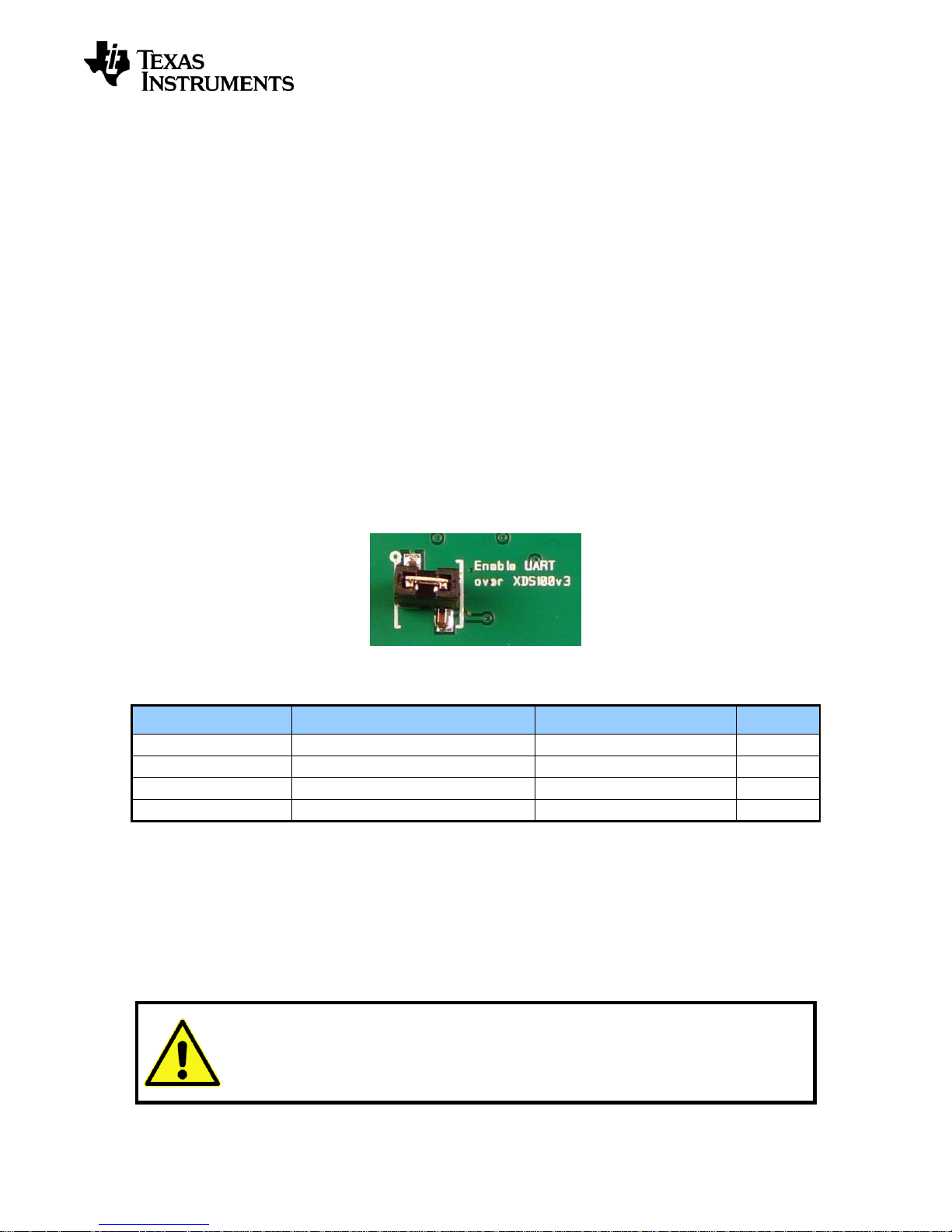
To enable the SmartRF06EB UART back channel the “Enable UART over XDS100v3” jumper
(J5), located on the lower right side of the EB, must be mounted (Figure 7). Table 4 shows an
overview of the I/O signals related to UART Back Channel.
Figure 7 – Jumper mounted on J5 to enable the UART back channel
Table 4 – UART Back channel signal connections
6.2 Power Sources
There are three ways to power the SmartRF06EB; batteries, USB bus and external power supply.
The power source can be selected using the power source selection switch (S502) seen in Figure
8. The XDS100v3 Emulator can only be powered over USB. The main power supply switch
(S501) cuts power to the SmartRF06EB.
Page 14/32
Page 15

User’s Guide
Do not power the SmartRF06EB using two 1.5 V AAA batteries and a 3 V CR2032
coin cell battery at the same time. Doing so may lead to excessive currents that may
damage the batteries or cause onboard components to break.
3
SWRU321A – May 2013
Figure 8 – Main power switch (P501) and source selection switch (P502)
6.2.1 USB Power
When the SmartRF06EB is connected to a PC via a USB cable, it can draw power from the USB
bus. The onboard voltage regulator supplies approximately 3.3 V to the mounted EM and the EB
peripherals. To power the mounted EM and the EB peripherals from the USB bus, the power
source selection switch (S502) should be in “USB” position (Figure 9).
The maximum current consumption is limited by the regulator to 1500 mA3.
Figure 9 – SmartRF06EB power selection switch (P502) in “USB” position
6.2.2 Battery Power
The SmartRF06EB can be powered using two 1.5 V AAA alkaline batteries or a 3 V CR2032 coin
cell battery. The battery holders for the AAA batteries and the CR2032 coin cell battery are
located on the reverse side of the PCB. To power the mounted EM and the EB peripherals using
batteries, the power source selection switch (S502) should be in “BAT” position (Figure 10).
When battery powered, the EM power domain is by default regulated to 2.1 V. The voltage
regulator may be bypassed by mounting a jumper on J502. See section 6.3.2 for more details.
Note that most USB power sources are limited to 500 mA.
Page 15/32
Page 16

User’s Guide
There is a risk of damaging the onboard components if the applied voltage on the
external power connector/header is lower than -0.3 V or higher than 3.6 V
(combined absolute maximum ratings for onboard components). See section 5.1 for
further information.
SWRU321A – May 2013
Figure 10 – SmartRF06EB power source selection switch (P502) in “BAT” position
6.2.3 External Power Supply
The SmartRF06EB can be powered using an external power supply. To power the mounted EM
and the EB peripherals using an external power supply, the power source selection switch (S502)
should be in “BAT” position (Figure 10 in section 6.2.2).
The external supply’s ground should be connected to the SmartRF06EB ground, e.g. to the
ground pad in the top left corner of the EB. Connect the positive supply connector to the external
power header J501 (Figure 11). The applied voltage must be in the range from 2.1 V to 3.6 V and
limited to max 1.5 A.
When powered by an external power supply, the EM power domain is by default regulated to
2.1 V. The voltage regulator may be bypassed by mounting a jumper on J502. See section 6.3.2
for more details.
Figure 11 – SmartRF06EB external power supply header (J501)
Page 16/32
Page 17

User’s Guide
XDS domain
(3.3 V)
XDS100v3, XDS LEDs
EM domain
(1.8 - 3.6 V)
ACC, ALS, keys, LEDs
3.3 V domain
(3.3 V)
LCD, SD card
Power sources
USB, batteries, external supply
Level
shifters
Level
shifters
Mounted EM
Component
Power domain
Power source
Evaluation Module
EM domain (LO_VDD)
USB, battery, external
General Purpose LEDs
EM domain (LO_VDD)
USB, battery, external
Accelerometer
EM domain (LO_VDD)
USB, battery, external
Ambient Light Sensor
EM domain (LO_VDD)
USB, battery, external
Current measurement MSP
MCU
EM domain (LO_VDD)
USB, battery, external
LEDs
EM domain (LO_VDD)
USB, battery, external
XDS100v3 Emulator
XDS domain
USB
XDS100v3 LEDs
XDS domain
USB
SD Card Slot
3.3 V domain (HI_VDD)
Same as EM domain
LCD
3.3 V domain (HI_VDD)
Same as EM domain
SWRU321A – May 2013
6.3 Power Domains
The SmartRF06EB is divided into three power domains, described in detail in the following
sections. The SmartRF06EB components, and what power domain they belong to, is shown in
Figure 12 and Table 5 below.
Figure 12 – Power domain overview of SmartRF06EB
Table 5 – Power domain overview of SmartRF06EB
6.3.1 XDS Domain
The XDS100v3 Emulator (see section 6.1) onboard the SmartRF06EB is in the XDS domain. The
XDS domain is powered over USB. The USB voltage supply (+5 V) is down-converted to +3.3 V
and +1.5 V for the different components of the XDS100v3 Emulator.
The SmartRF06EB must be connected to e.g. a PC over USB for the XDS domain to be powered
up. The domain is turned on/off by the SmartRF06EB main power switch.
6.3.2 EM Domain
The mounted EM board and most of the SmartRF06EB peripherals are powered in the EM
domain and signals in this domain (accessible by the EM), are prefixed “LV_” in the schematics.
Table 5 lists the EB peripherals that are powered in the EM domain. The domain is turned on/off
by the SmartRF06EB power switch.
Page 17/32
Page 18

User’s Guide
The LCD connector on SmartRF06EB is very tight to ensure proper contact between
the EM and the LCD. Be extremely cautious when removing the LCD to avoid the
display from breaking.
NOTE: Mounting a jumper on J502 will not have any effect if the SmartRF06EB is powered
over USB (when the power source selection switch, S502, is in “USB” position).
SWRU321A – May 2013
The EM domain may be powered using various power sources; USB powered (regulated to 3.3
V), battery powered (regulated to 2.1 V or unregulated) and using an external power supply
(regulated to 2.1 V or unregulated).
When battery powered or powered by an external source, the EM power domain is by default
regulated to 2.1 V using a step down converter. The step down converter may be bypassed by
mounting a jumper on J502 (Figure 13), powering the EM domain directly from the source. When
J502 is not mounted, the EM power domain is regulated to 2.1 V. The maximum current
consumption of the EM power domain is then limited by the regulator to 410 mA.
Figure 13 – Mount a jumper on J502 to bypass EM domain voltage regulator
6.3.3 3.3 V Domain
The 3.3 V domain is a sub domain of the EM domain. The 3.3 V domain is regulated to 3.3 V
using a buck-boost converter, irrespective of the source powering the EM domain. Signals in the
3.3V domain (controlled by the EM) are prefixed “HV_” for High Voltage in the schematics.
Two EB peripherals are in the 3.3 V domain, the LCD and the SD card slot, as listed in Table 5.
These peripherals are connected to the EM domain via level shifters U401 and U402.
The 3.3 V domain may be switched on (off) completely by the mounted EM board by pulling
signal LV_3.3V_EN to a logical 1 (0). See Table 14 in section 6.11.1 for details about the
mapping between the EM and signals onboard the SmartRF06EB.
6.4 LCD
The SmartRF06EB comes with a 128x64 pixels display from Electronic Assembly (DOGM128E-6)
[4]. The LCD display is available to mounted EM via a SPI interface, enabling software
development of user interfaces and demo use. Table 6 shows an overview of the I/O signals
related to the LCD.
The recommended operating condition for the LCD display is a supply voltage between 3.0 V and
3.3 V. The LCD display is powered from the 3.3 V power domain (HI_VDD). The min (max)
operating temperature is -20 (+70) ˚C.
Page 18/32
Page 19

User’s Guide
Signal name
Description
Probe header
EM pin
LV_3.3V_EN
3.3 V domain enable signal4
RF1.15 (P407.1)
RF1.15
LV_LCD_MODE
LCD mode signal
RF1.11 (P406.7)
RF1.11
¯¯¯¯¯¯¯¯¯¯¯¯¯¯LV_LCD_RESET
LCD reset signal (active low)
RF1.13 (P406.9)
RF1.13
¯¯¯¯¯¯¯¯¯¯LV_LCD_CS
LCD Chip Select (active low)
RF1.17 (P407.3)
RF1.17
LV_SPI_SCK
SPI Clock
RF1.16_SCK (P407.2)
RF1.16
LV_SPI_MOSI
SPI MOSI (LCD input)
RF1.18_MOSI (P407.4)
RF1.18
Signal name
Description
Probe header
EM pin
LV_3.3V_EN
3.3 V domain enable signal4
RF1.15 (P407.1)
RF1.15
¯¯¯¯¯¯¯¯¯¯¯¯¯¯LV_SDCARD_CS
SD card Chip Select (active low)
RF2.12 (P411.1)
RF2.12
LV_SPI_SCK
SPI Clock
RF1.16_SCK (P407.2)
RF1.16
LV_SPI_MOSI
SPI MOSI (SD card input)
RF1.18_MOSI (P407.4)
RF1.18
LV_SPI_MISO
SPI MISO (SD card output)
RF1.20_MISO (P407.5)
RF1.20
Signal name
Description
Probe header
EM pin
LV_ACC_PWR
Acc. power enable signal
RF2.8 (P407.8)
RF2.8
LV_ACC_INT1
Acc. interrupt signal
RF2.16 (P411.5)
RF2.16
LV_ACC_INT2
Acc. interrupt signal
RF2.14 (P411.3)
RF2.14
¯¯¯¯¯¯¯¯¯¯¯LV_ACC_CS
Acc. Chip Select (active low)
RF2.10 (P407.9)
RF2.10
LV_SPI_SCK
SPI Clock
RF1.16_SCK (P407.2)
RF1.16
LV_SPI_MOSI
SPI MOSI (acc. input)
RF1.18_MOSI (P407.4)
RF1.18
4
SWRU321A – May 2013
Table 6 – LCD signal connections
6.5 Micro SD Card Slot
The SmartRF06EB has a micro SD card slot for connecting external SD/MMC flash devices (flash
device not included). A connected flash device is available to the mounted EM via a SPI interface,
giving it access to extra flash, enabling over-the-air upgrades and more. Table 8 shows an
overview of I/O signals related to the micro SD card slot.
The micro SD card is powered from the 3.3 V power domain (HI_VDD).
Table 7 – Micro SD Card signal connections
6.6 Accelerometer
The SmartRF06EB is equipped with a BMA250 digital accelerometer from Bosch Sensortech [6].
The accelerometer is available to the mounted EM via an SPI interface and has two dedicated
interrupt lines. The accelerometer is suitable for application development, prototyping and demo
use. Table 8 shows an overview of I/O signals related to the accelerometer.
The recommended operating condition for the accelerometer is a supply voltage between 1.62 V
and 3.6 V. The min (max) operating temperature is -40 (+85) ˚C.
The LCD and SD card are both powered in the 3.3 V domain and cannot be powered on/off individually.
Page 19/32
Page 20

User’s Guide
LV_SPI_MISO
SPI MISO (acc. output)
RF1.20_MISO (P407.5)
RF1.20
Ambient Light Sensor
LV_ALS_OUT
LV_ALS_PWR
22 kOhm
Signal name
Description
Probe header
EM pin
LV_ALS_PWR
ALS power enable signal
RF2.6 (P407.7)
RF2.6
LV_ALS_OUT
ALS output signal (analog)
RF2.5 (P411.6)
RF2.5
Signal name
Description
Probe header
EM pin
LV_BTN_LEFT
Left button (active low)
RF1.6 (P406.4)
RF1.6
LV_BTN_RIGHT
Right button (active low)
RF1.8 (P406.5)
RF1.8
LV_BTN_UP
Up button (active low)
RF1.10 (P406.6)
RF1.10
LV_BTN_DOWN
Down button (active low)
RF1.12 (P406.8)
RF1.12
LV_BTN_SELECT
Select button (active low)
RF1.14 (P406.10)
RF1.14
¯¯¯¯¯¯¯¯¯¯¯¯¯¯LV_BTN_RESET
EM reset button (active low)
RF2.15_RESET¯¯¯¯¯¯¯¯¯¯¯¯¯ (P411.4)
RF2.15
SWRU321A – May 2013
Table 8 – Accelerometer signal connections
6.7 Ambient Light Sensor
The SmartRF06EB has an analog SFH 5711 ambient light sensor (ALS) from Osram [7] that is
available for the mounted EM via the EM connectors, enabling quick application development for
demo use and prototyping. Figure 14 and Table 9 shows an overview of I/O signals related to the
ambient light sensor.
The recommended operating condition for the ambient light sensor is a supply voltage between
2.3 V and 5.5 V. The min (max) operating temperature is -40 (+85) ˚C.
Figure 14 – Simplified schematic of Ambient Light Sensor setup
Table 9 – Ambient Light Sensor signal connections
6.8 Buttons
There are 6 buttons on the SmartRF06EB. Status of the LEFT, RIGHT, UP, DOWN and SELECT
buttons are available to the mounted EM. These buttons are intended for user interfacing and
development of demo applications.
The EM RESET button resets the mounted EM by pulling its reset line low (RF2.15_RESET¯¯¯¯¯¯¯¯¯¯¯¯¯).
Table 10 shows an overview of I/O signals related to the buttons.
Page 20/32
Table 10 – Button signal connections
Page 21

User’s Guide
Signal name
Description
Probe header
EM pin
LV_LED_1
LED 1 (red)
RF2.11 (P407.10)
RF2.11
LV_LED_2
LED 2 (yellow)
RF2.13 (P411.2)
RF2.13
LV_LED_3
LED 3 (green)
RF1.2 (P406.1)
RF1.2
LV_LED_4
LED 4 (red-orange)
RF1.4 (P406.2)
RF1.4
SWRU321A – May 2013
6.9 LEDs
6.9.1 General Purpose LEDs
The four LEDs D601, D602, D603, D604 can be controlled from the mounted EM and are suitable
for demo use and debugging. The LEDs are active high. Table 11 shows an overview of I/O
signals related to the LEDs.
Table 11 – General purpose LED signal connections
6.9.2 XDS100v3 Emulator LEDs
The XDS100v3 emulator has two LEDs to indicate its status, D2 and D4. The LEDs are located
on the top side of the SmartRF06EB. LED D2 is lit whenever the XDS100v3 Emulator is powered,
while LED D4 (ADVANCED MODE) is lit when the XDS100v3 is in an active cJTAG debug state.
6.10 EM Connectors
The EM connectors, shown in Figure 15, are used for connecting an EM board to the
SmartRF06EB. The connectors RF1 and RF2 are the main interface and are designed to inhibit
incorrect mounting of the EM board. The pin-out of the EM connectors is given in Table 12 and
Table 13.
Figure 15 – SmartRF06EB EM connectors RF1 and RF2
Page 21/32
Page 22

User’s Guide
EM pin
Signal name
Description
Probe
header
Breakout
header
RF1.1
GND
Ground
RF1.2
RF1.2
GPIO signal to EM board
P406.1
P403.1-2
RF1.3
RF1.3_UART_CTS
UART back channel / GPIO
P412.4
P408.15-16
RF1.4
RF1.4
GPIO signal to EM board
P406.2
P403.3-4
RF1.5
RF1.5
GPIO signal to EM board
P406.3
P403.5-6
RF1.6
RF1.6
GPIO signal to EM board
P406.4
P403.7-8
RF1.7
RF1.7_UART_RX
UART back channel (EM RX)
P412.2
P408.11-12
RF1.8
RF1.8
GPIO signal to EM board
P406.5
P403.9-10
RF1.9
RF1.9_UART_TX
UART back channel (EM TX)
P412.3
P408.13-14
RF1.10
RF1.10
GPIO signal to EM board
P406.6
P403.11-12
RF1.11
RF1.11
GPIO signal to EM board
P406.7
P403.13-14
RF1.12
RF1.12
GPIO signal to EM board
P406.8
P403.15-16
RF1.13
RF1.13
GPIO signal to EM board
P406.9
P403.17-18
RF1.14
RF1.14
GPIO signal to EM board
P406.10
P403.19-20
RF1.15
RF1.15
GPIO signal to EM board
P407.1
P404.1-2
RF1.16
RF1.16_SPI_SCK
EM SPI Clock
P407.2
P404.3-4
RF1.17
RF1.17
GPIO signal to EM board
P407.3
P404.5-6
RF1.18
RF1.18_SPI_MOSI
EM SPI MOSI
P407.4
P404.7-8
RF1.19
GND
Ground
RF1.20
RF1.20_SPI_MISO
EM SPI MISO
P407.5
P404.9-10
EM pin
Signal name
Description
Probe
header
Breakout
header
RF2.1
RF2.1_JTAG_TCK
JTAG Test Clock
P409.9
P408.1-2
RF2.2
GND
Ground
RF2.3
RF_VDD2
EM power
TP10
J503.1-2
RF2.4
RF2.4_JTAG_TMS
JTAG Test Mode Select
P409.7
P408.3-4
RF2.5
RF2.5
GPIO signal to EM board
P407.6
P404.11-12
RF2.6
RF2.6
GPIO signal to EM board
P407.7
P404.13-14
RF2.7
RF_VDD1
EM power
TP10
J503.1-2
RF2.8
RF2.8
GPIO signal to EM board
P407.8
P404.15-16
RF2.9
RF_VDD1
EM power
TP10
J503.1-2
RF2.10
RF2.10
GPIO signal to EM board
P407.9
P404.17-18
RF2.11
RF2.11
GPIO signal to EM board
P407.10
P404.19-20
RF2.12
RF2.12
GPIO signal to EM board
P411.1
P405.1-2
RF2.13
RF2.13
GPIO signal to EM board
P411.2
P405.3-4
RF2.14
RF2.14
GPIO signal to EM board
P411.3
P405.5-6
RF2.15
RF2.15_RESET¯¯¯¯¯¯¯¯¯¯¯¯¯
EM reset signal (active low)
P411.4
P405.7-8
RF2.16
RF2.16
GPIO signal to EM board
P411.5
P405.9-10
RF2.17
RF2.17_JTAG_TDI
GPIO / JTAG Test Data In
P409.5
P408.5-6
RF2.18
RF2.18_UART_RTS
GPIO / UART Back Channel
P412.5
P408.17-18
RF2.19
RF2.19_JTAG_TDO
GPIO / JTAG Test Data Out
P409.13
P408.7-8
RF2.20
GND
Ground
SWRU321A – May 2013
Table 12 – EM connector RF1 pin-out
Page 22/32
Table 13 – EM connector RF2 pin-out
Page 23

User’s Guide
Evaluation
Module
Peripheral
probe headers
P406, P407,
P411
I/O breakout headers
P403, P404, P405
SmartRF06EB
peripherals
ACC, ALS, keys, LCD,
LED, SD card
XDS bypass header
P408
XDS100v3
Emulator
20-pin
ARM-JTAG
Debug Header
P409
10-pin Cortex
Debug Header
P410
UART back
channel probe
header
P412
NOTE: By default, all jumpers are mounted on P403, P404, P405 and P408. The default
configuration is assumed in this user’s guide unless otherwise stated.
SWRU321A – May 2013
6.11 Breakout Headers and Jumpers
The SmartRF06EB has several breakout headers, giving access to all EM connector pins. An
overview of the SmartRF06EB I/O breakout headers is given in Figure 16. Probe headers P406,
P407, P411 and P412 give access to the I/O signals of the mounted EM. Breakout headers P403,
P404 and P405 allow the user to map any EM I/O signal to any peripheral on the SmartRF06EB.
The XDS bypass header (P408) makes it possible to disconnect the XDS100v3 Emulator
onboard the EB from the EM. Using the 20-pin ARM JTAG header (P409) or the 10-pin ARM
Cortex Debug Header (P410), it is possible to debug external targets using the onboard emulator.
Figure 16 – SmartRF06EB I/O breakout overview
6.11.1 I/O Breakout Headers
The I/O breakout headers on SmartRF06EB consist of pin connectors P406, P407, P411 and
P412. P406, P407 and P411 are located at the top left side of SmartRF06EB. All EM signals
available on these probe headers can be connected to or disconnected from SmartRF06EB
peripherals using jumpers on headers P403, P404, P405.
Probe header P412 is located near the bottom right corner of the SmartRF06EB. The signals
available on P412 are connected to the XDS100v3 Emulator’s UART back channel using jumpers
on header P408.
The I/O breakout mapping between the SmartRF06EB and the mounted EM is given in Table 14.
The leftmost column in the below table refers to the silk print seen on the SmartRF06EB. The
rightmost column shows the corresponding CC2538 I/O pad on CC2538EM.
Page 23/32
Page 24

User’s Guide
Probe
header
Silk print
EB signal name
EM
connector
CC2538EM
I/O
P406
RF1.2
LV_LED_3
RF1.2
PC2
RF1.4
LV_LED_4
RF1.4
PC3
RF1.5
NC
RF1.5
PB1
RF1.6
LV_BTN_LEFT
RF1.6
PC4
RF1.8
LV_BTN_RIGHT
RF1.8
PC5
RF1.10
LV_BTN_UP
RF1.10
PC6
RF1.11
LV_LCD_MODE
RF1.11
PB2
RF1.12
LV_BTN_DOWN
RF1.12
PC7
RF1.13
¯¯¯¯¯¯¯¯¯¯¯¯¯¯LV_LCD_RESET
RF1.13
PB3
RF1.14
LV_BTN_SELECT
RF1.14
PA3
P407
RF1.15
LV_3.3V_EN
RF1.15
PB4
RF1.16_SCK
LV_SPI_SCK
RF1.16
PA2
RF1.17
¯¯¯¯¯¯¯¯¯¯LV_LCD_CS
RF1.17
PB5
RF1.18_MOSI
LV_SPI_MOSI
RF1.18
PA4
RF1.20_MISO
LV_SPI_MISO
RF1.20
PA5
RF2.5
LV_ALS_OUT
RF2.5
PA6
RF2.6
LV_ALS_PWR
RF2.6
PA7
RF2.8
LV_ACC_PWR
RF2.8
PD4
RF2.10
¯¯¯¯¯¯¯¯¯¯¯LV_ACC_CS
RF2.10
PD5
RF2.11
LV_LED_1
RF2.11
PC0
P411
RF2.12
¯¯¯¯¯¯¯¯¯¯¯¯¯¯LV_SDCARD_CS
RF2.12
PD0
RF2.13
LV_LED_2
RF2.13
PC1
RF2.14
LV_ACC_INT2
RF2.14
PD1
RF2.15_RESET
¯¯¯¯¯¯¯¯¯¯¯¯¯¯LV_BTN_RESET
RF2.15
nRESET
RF2.16
LV_ACC_INT1
RF2.16
PD2
P412
EM_UART_RX
RF1.7_UART_RX
RF1.7
PA0
EM_UART_TX
RF1.9_UART_TX
RF1.9
PA1
EM_UART_CTS
RF1.3_UART_CTS
RF1.3
PB0
EM_UART_RTS
RF2.18_UART_RTS
RF2.18
PD3
SWRU321A – May 2013
Table 14 – SmartRF06EB I/O breakout overview
6.11.2 XDS100v3 Emulator Bypass Headers
The XDS100v3 Emulator bypass header, P408, is by default mounted with jumpers (Figure 17),
connecting the XDS100v3 Emulator to a mounted EM or external target. By removing the jumpers
on P408, the XDS100v3 Emulator may be disconnected from the target.
Figure 17 – XDS100v3 Emulator Bypass Header (P408)
Page 24/32
Page 25

User’s Guide
Pin
Signal
Description
EB signal name
XDS
bypass
header
P409.1
VTRef
Voltage reference
VDD_SENSE
P408.19-20
P409.2
VSupply
Voltage supply
NC
P409.3
nTRST
Test Reset
NC
P409.4
GND
Ground
GND
P409.5
TDI
Test Data In
RF2.17_JTAG_TDI
P408.5-6
P409.6
GND
Ground
GND
P409.7
TMS
Test Mode Select
RF2.4_JTAG_TMS
P408.3-4
P409.8
GND
Ground
GND
P409.9
TCK
Test Clock
RF2.1_JTAG_TCK
P408.1-2
P409.10
GND
Ground
GND
P409.11
RTCK
Return Clock
NC
P409.12
GND
Ground
GND
P409.13
TDO
Test Data Out
RF2.19_JTAG_TDO
P408.7-8
P409.14
GND
Ground
GND
P409.15
nSRST
System Reset
RF2.15_RESET¯¯¯¯¯¯¯¯¯¯¯¯¯
P408.9-10
P409.16
GND
Ground
GND
P409.17
DBGRQ
Debug Request
NC
P409.18
GND
Ground
GND
P409.19
DBGACK
Debug Acknowledge
NC
P409.20
GND
Ground
GND
SWRU321A – May 2013
6.11.3 20-pin ARM JTAG Header
The SmartRF06EB comes with a standard 20-pin ARM JTAG header [8] (Figure 18), enabling the
user to debug an external target using the XDS100v3 Emulator. The pin-out of the ARM JTAG
header is given in Table 15. Chapter 7 has more information on how to debug an external target
using the XDS100v3 Emulator onboard the SmartRF06EB.
Figure 18 – 20-pin ARM JTAG header (P409)
Table 15 – 20-pin ARM JTAG header pin-out (P409)
Page 25/32
Page 26

User’s Guide
Pin
Signal
Description
EB signal name
XDS bypass
header
P410.1
VCC
Voltage reference
VDD_SENSE
P408.19-20
P410.2
TMS
Test Mode Select
RF2.4_JTAG_TMS
P408.3-4
P410.3
GND
Ground
GND
P410.4
TCK
Test Clock
RF2.1_JTAG_TCK
P408.1-2
P410.5
GND
Ground
GND
P410.6
TDO
Test Data Out
RF2.19_JTAG_TDO
P408.7-8
P410.7
KEY
Key
NC P410.8
TDI
Test Data In
RF2.17_JTAG_TDI
P408.5-6
P410.9
GNDDetect
Ground detect
GND
P410.10
nRESET
System Reset
RF2.15_RESET¯¯¯¯¯¯¯¯¯¯¯¯¯
P408.9-10
SWRU321A – May 2013
6.11.4 10-pin ARM Cortex Debug Header
The SmartRF06EB comes with a standard 10-pin ARM Cortex debug header [8] (Figure 19),
enabling the user to debug an external target using the XDS100v3 Emulator. The ARM Cortex
debug header is located near the right hand edge of the EB. The header pin-out is given in Table
16. Chapter 7 has more information on how to debug an external target using the XDS100v3
Emulator onboard the SmartRF06EB.
Figure 19 – 10-pin ARM Cortex Debug header (P410)
Table 16 – 10-pin ARM Cortex Debug header pin-out (P410)
Page 26/32
Page 27

User’s Guide
15
V
I
CURMEAS
EM
G = 100
0.15 Ohm
To EM
I
EM
V
CURMEAS
SWRU321A – May 2013
6.12 Current Measurement
The SmartRF06EB provides two options for easy measurements of the current consumption of a
mounted EM. The following sections describe these two options in detail.
6.12.1 High-side current sensing
The SmartRF06EB comes with a current sensing unit for measuring the current consumption of
the mounted EM (Figure 20). The current sensing setup is “high-side”, that is, it measures the
current going to the mounted EM. The current is converted to a voltage, available at the
CURMEAS_OUTPUT test point (TP11), located near the right edge of the SmartRF06EB. Using
the SmartRF06EB together with for example an oscilloscope makes it easy to measure the EM
current consumption as a function of time.
The relationship between the voltage measured at CURMEAS_OUTPUT, V
current consumption, IEM, is given by Equation 1 below.
CURMEAS
, and the EM
(1)
Figure 20 – Simplified schematic of high-side current sensing setup
6.12.2 Current Measurement Jumper
SmartRF06EB has a current measurement header, J503, for easy measurement of EM current
consumption. Header J503 is located on the upper right hand side of the EB. By replacing the
jumper with an ammeter, as shown in Figure 21, the current consumption of the mounted EM can
be measured.
Figure 21 – Measuring current consumption using jumper J503
Page 27/32
Page 28

User’s Guide
Having a jumper mounted on header J503 when debugging an external target will
cause a conflict between the EB’s EM domain supply voltage and the target’s supply
voltage. This may result in excess currents, damaging the onboard components of
the SmartRF06EB or the target board.
XDS100v3
06EB XDS + EM
EM
(EM domain)
XDS100v3
06EB XDS + external target
Ext. target
(Target VDD)
EM
(EM domain)
XDS100v3
External debugger + EM
External
debugger
EM
(EM domain)
P408
(jumpers on)
P408
(jumpers off)
J503
(mounted)
J503
(mounted)
J503
(not mounted)
Current measurement jumper
XDS bypass header
P408
(jumpers on)
Debug
header
P409/P410
P409/P410
SWRU321A – May 2013
7 Debugging an external target using SmartRF06EB
You can easily use XDS100v3 Emulator onboard the SmartRF06EB to debug an external target.
It is in this chapter assumed that the target is self-powered.
When debugging an external, self-powered target using SmartRF06EB, make sure to remove the
jumper from the current measurement header (J503) as shown in the second scenario of Figure
22. In this scenario, the onboard XDS100v3 senses the target voltage of the external target. In
the left side scenario of the same figure, the XDS100v3 senses the target voltage of the EB’s EM
domain.
In Figure 22, the right hand side scenario shows how it is possible to debug an EM mounted on
the SmartRF06EB using an external debugger. In this scenario, all the jumpers must be removed
from the SmartRF06EB header P408 to avoid signaling conflicts between the onboard XDS100v3
Emulator and the external debugger.
Figure 22 – Simplified connection diagram for different debugging scenarios
Page 28/32
Page 29

User’s Guide
SWRU321A – May 2013
7.1 20-pin ARM JTAG Header
The SmartRF06EB has a standard 20-pin ARM JTAG header mounted on the right hand side
(P409). Make sure all the jumpers on the XDS bypass header (P408) are mounted and that the
jumper is removed from header J503.
Connect the external board to the 20-pin ARM JTAG header (P409) using a 20-pin flat cable as
seen in Figure 23. Make sure pin 1 on P409 matches pin 1 on the external target. See sections
6.11.3 and 6.11.2 for more info about the 20-pin ARM JTAG header and the XDS bypass header,
respectively.
Figure 23 – Debugging external target using SmartRF06EB
7.2 10-pin ARM Cortex Debug Header
The SmartRF06EB has a standard 10-pin ARM Cortex Debug header mounted on the right hand
side (P410). Make sure all the jumpers on the XDS bypass header (P408) are mounted and that
the jumper is removed from header J503.
Connect the external board to the 10-pin ARM JTAG header using a 10-pin flat cable. Make sure
pin 1 on P410 matches pin 1 on the external target See sections 6.11.4 and 6.11.2 for more info
about the 10-pin ARM Cortex Debug header and the XDS bypass header, respectively.
Page 29/32
Page 30

User’s Guide
EB Signal Name
EB
Breakout
Description
VDD_SENSE
P409.1
Target voltage supply
GND
P409.4
Common ground for EB and external board
RF2.1_JTAG_TCK
P409.9
Test Clock
RF2.4_JTAG_TMS
P409.7
Test Mode Select
EB Signal Name
EB
Breakout
Description
RF2.17_JTAG_TDI
P409.5
Test Data In (optional for cJTAG)
RF2.19_JTAG_TDO
P409.13
Test Data Out (optional for cJTAG)
RF2.15_RESET¯¯¯¯¯¯¯¯¯¯¯¯¯
P409.15
Target reset signal (optional)
VDD_SENSE
RF2.17_JTAG_TDI
RF2.4_JTAG_TMS
RF2.1_JTAG_TCK
RF2.19_JTAG_TDO
GND
2-pin cJTAG
4-pin JTAG
Optional
+
RF2.15_RESET
SWRU321A – May 2013
7.3 Custom Strapping
If the external board does not have a 20-pin ARM JTAG connector nor a 10-pin ARM Cortex
connector, the needed signals may be strapped from the onboard XDS100v3 Emulator to the
external target board.
Make sure all the jumpers on the XDS bypass header (P408) are mounted and that the jumper is
removed from header J503. Table 17 shows the signals that must be strapped between the
SmartRF06EB and the target board. Table 18 shows additional signals that are optional or
needed for debugging using 4-pin JTAG. Figure 24 shows where the signals listed in Table 17
and Table 18 can be found on the 20-pin ARM JTAG header.
Table 17 – Debugging external target: Minimum strapping (cJTAG support)
Table 18 – Debugging external target: Optional strapping
Page 30/32
Figure 24 – ARM JTAG header (P409) with strapping to debug external target
Page 31

User’s Guide
SWRU321A – May 2013
8 Frequently Asked Questions
Q1 Nothing happens when I power up the evaluation board. Why?
A1 Make sure you have a power source connected to the EB. Verify that the power source
selection switch (S502) is set correctly according to your power source. When powering
the EB from either batteries or an external power source, S502 should be in “BAT”
position. When powering the EB over USB, the switch should be in “USB” position. Also,
make sure the EM current measurement jumper (J503) is short circuited.
Q2 Why are there two JTAG connectors on the SmartRF06EB, which one should I use?
A2 The SmartRF06EB comes with two different standard debug connectors, the 20-pin ARM
JTAG connector (P409) and the compact 10-pin ARM Cortex debug connector (P410).
These debug connectors are there to more easily debug external targets without the
need of customized strapping. For more details on how to debug external targets using
the SmartRF06EB, see chapter 7.
Q3 Can I use the SmartRF06EB to debug an 8051 SoC such as CC2530?
A3 No, you cannot debug an 8051 SoC using the SmartRF06EB.
Q4 When connecting my SmartRF06EB to my PC, no serial port appears. Why?
A4 It may be that the virtual COM port on the SmartRF06EB’s XDS100 channel B hasn’t
been enabled. Section 4.1.2.1.1 describes how to enable the Vritual COM Port in the
USB driver.
Page 31/32
Page 32

User’s Guide
Revision
Date
Description/Changes
SWRU321A
2013-05-21
Minor fixes to Figure 4. Fixed incorrect EM mapping in Table 11.
Added steps for installing SmartRF06EB on Linux.
SWRU321
2012-09-07
Initial version.
SWRU321A – May 2013
9 References
[1] SmartRF Studio Product Page
http://www.ti.com/tool/smartrftm-studio
[2] FTDI USB Driver Page
http://www.ftdichip.com
[3] SmartRF Flash Programmer Product Page
http://www.ti.com/tool/flash-programmer
[4] XDS100 Emulator Product Page
http://processors.wiki.ti.com/index.php/XDS100
[5] Electronic Assembly DOGM128-6 Datasheet
http://www.lcd-module.com/eng/pdf/grafik/dogm128e.pdf
[6] Bosch Sensortec BMA250 Datasheet
http://ae-bst.resource.bosch.com/media/products/dokumente/bma250/bst-bma250ds002-05.pdf
[7] Osram SFH 5711
http://www.osram-os.com
[8] Cortex-M Debug Connectors
http://infocenter.arm.com/help/topic/com.arm.doc.faqs/attached/13634/cortex_debu
g_connectors.pdf
10 Document History
Page 32/32
Page 33

User’s Guide
SWRU321A – May 2013
Appendix A
Schematics
SmartRF06EB 1.2.1
Page 34

LOW VOLTAGE
PERIPHERALS
XDS100v3 - FPGA
XDS100v3 - FTDI
EM INTERFACE/
LEVEL SHIFTERS
POWER SUPPLY
HIGH VOLTAGE
PERIPHERALS
1
FM2
FIDUCIAL_MARK_1mm
1
FM4
FIDUCIAL_MARK_1mm
H2
HOLE_3H3HOLE_3
1
FM5
FIDUCIAL_MARK_1mm
H1
HOLE_3
1
FM6
FIDUCIAL_MARK_1mm
1
FM1
FIDUCIAL_MARK_1mm
H4
HOLE_3
1
FM3
FIDUCIAL_MARK_1mm
TP13
TESTPOINT_PAD
TP12
TESTPOINT_PAD
ISSUED
1(7)
SmartRF06EB
- Top Level
SCALE
SHEET
REV.
DWG NO.
DWG
COMPANY NAME
FSCM NO.
SIZE
CONTRACT NO.
Texas Instruments
A3
DRAWN
13/07/12
13/07/12
12/07/12
MAW
1.2.1
DATE
APPROVALS
CHECKED
Page 35

PRG_TDO
EXT_SELECT
ADV_MODE
V_USB V_USB
RESET_N
VCCPLF
T_TVD
VTARGET
UART_EN_N
P3.3VXDS
P1.8V
P3.3VXDS
P3.3VXDS
+1.5V
P3.3VXDS P3.3VXDS
P3.3VXDS
P3.3VXDS
P3.3VXDS
P3.3VXDS
P3.3VXDS
P3.3VXDS
1
2
3
4
STANDBY
VDD
OUTPUT
ASDM
GND
O1
ASDM 100.000MHZ
1
2
3
Q1
BC846
1
2
3
4
5
6
7
8
9
10
INA+
INA-
OUTA
OUTB
V+
INB+
OPA2363
INB-
V-
ENB
ENA
U6
OPA2363
123456789101112131415161718192021222324
25
26
27
28
29
30
31
32
33
34
35
36
37
38
39
40
41
42
43
44
45
46
47
48
49
50
515253 5455565758 5960616263 6465666768 6970717273 74
75
76
77
78
79
80
81
82
83
84
85
86
87
88
89
90
91
92
93
94
95
96
97
98
99
100
GND
GND
GND
GND
GND
UART_EN_N
GND
VCCPLF
CLK_100M
P1.5V
P3.3VXDS
RESET_N
DTSA_BYP
CBL_DIS
EMU1
POD_RLS
P3.3VXDS
TVD
CLK_FAIL
SRST_OUT
RTCK
EMU0
EMU_EN
TRST
TMS
TDO
TDI
TCK
P1.5V
P3.3VXDS
SUSPEND
ALT_FUNC
PRG_TCK
PRG_TMS
PRG_TDI
PRG_TDO
PRG_TCK
PRG_TDI
PRG_TMS
P3.3VXDS
P3.3VXDS
PRG_TDO
PRG_TRST
P3.3VXDS
VTARGET
P1.5V
VTARGET
PWRGOOD
VTARGET
P1.5V
ADV_MODE
EXT_SELECT
T_DIS
VTARGET
IO32RSB0
GBC0/IO35RSB0
IO13RSB0
GAA0/IO00RSB0
GBC1/IO36RSB0
IO15RSB0
GAA1/IO01RSB0
GAC1/IO05RSB0
GBB0/IO37RSB0
IO19RSB0
GNDQ
GBA2/IO41RSB0
GBA0/IO39RSB0
GBB1/IO38RSB0
GBA1/IO40RSB0
GCC2/IO59RSB0
GBB2/IO43RSB0
GDC1/IO61RSB0
IO09RSB0
GCC1/IO51RSB0
GDC0/IO62RSB0
GCC0/IO52RSB0
VMV0
GDA1/IO65RSB0
VCCIB0
GAB1/IO03RSB0
GCA1/IO55RSB0
TDO
VCC
GBC2/IO45RSB0
VCC
VJTAG
VCC
VCCIB1
VCC
IO11RSB0
VMV1
NC
GCA0/IO56RSB0
TMS
GAC0/IO04RSB0
TRST
GDA2/IO70RSB1
IO84RSB1
TDI
VPUMP
IO87RSB1
GDB2/IO71RSB1
IO42RSB0
IO93RSB1
IO75RSB1
TCK
IO96RSB1
IO94RSB1
GDC2/IO72RSB1
IO97RSB1
IO81RSB1
GND
IO95RSB1
IO99RSB1
GCB2/IO58RSB0
GND
IO100RSB1
IO47RSB0
IO102RSB1
GEC2/IO104RSB1
GEB2/IO105RSB1
GEA2/IO106RSB1
GNDQ
VMV1
GEA0/IO107RSB1
GND
GEA1/IO108RSB1
GEB0/IO109RSB1
GEB1/IO110RSB1
GEC0/IO111RSB1
GFA2/IO120RSB1
GFA1/IO121RSB1
VCCPLF
GFA0/IO122RSB1
VCOMPLF
GFB0/IO123RSB1
GFB1/IO124RSB1
IO129RSB1
IO130RSB1
GAC2/IO131RSB1
IO132RSB1
GAA2/IO67RSB1
GND
GAB2/IO69RSB1
GND
VCCIB1
VCCIB0
GND
IO68RSB1
IO28RSB0
IO25RSB0
IO22RSB0
IO07RSB0
GAB0/IO02RSB0
A3PN125-ZVQG100
U11
A3PN125-VQFP
1
2
C23
C_4U7_0603_X5R_K_6
1
2
C27
C_4U7_0603_X5R_K_6
1
2
C26
C_4U7_0603_X5R_K_6
1
2
C24
C_100N_0402_X5R_K_10
1
2
C22
C_100N_0402_X5R_K_10
1
2
C21
C_100N_0402_X5R_K_10
1
2
C25
C_100N_0402_X5R_K_10
2
1
D1
CDBP0130L-G
1
2
R1
L_BEAD_102_0402
1
2
D4
LED_EL19-21SRC
1
2
J5
PINROW_SMD_1X2_2.54MM
1
2
T_TMS
R47
R_10K_0402_F
1
2
R50
R_1K0_0402_F
1
2
R49
R_1K0_0402_F
1
2
R27
R_1K0_0402_F
1
2
R24
R_5K1_0402_J
1
2
R54
R_5K1_0402_J
1
2
R41
R_10K_0402_F
1
2
R48
R_10K_0402_F
1
2
R46
R_10K_0402_F
1
2
PWRGOOD
R31
R_10K_0402_F
1
2
PRG_TMS
R43
R_10K_0402_F
1
2
R44
R_10K_0402_F
1
2
T_EMU4
R52
R_51_0402_G
1
2
T_EMU2
R51
R_51_0402_G
1
2
T_EMU3
R53
R_51_0402_G
1
2
T_TDI
R18
R_51_0402_G
1
2
T_RTCK
R23
R_51_0402_G
1
2
T_TRST
R19
R_51_0402_G
1
2
T_EMU5
R55
R_51_0402_G
1
2
T_TMS
R15
R_51_0402_G
1
2
T_TDO
R16
R_51_0402_G
1
2
T_TCK
R17
R_51_0402_G
1
2
CLK_100M
R33
R_51_0402_G
1
2
R30
R_120K_0402_F
1
2
R29
R_120K_0402_F
1
2
R25
R_120K_0402_F
1
2
R42
R_220_0402_J
1
2
T_EMU1
R20
R_470_0402_F
1
2
T_EMU0
R22
R_470_0402_F
1
2
T_SRST
R21
R_470_0402_F
1
2
C34
C_15N_0402_X7R_K_25
1
2
T_DIS
R12
R_0_0402
1
2
3
4
5
T_TVD
T_TDI
T_TDO
T_RTCK
IO3
IO2
IO1
GND
TPD4E002
IO4
U8
TPD4E002
1
2
3
4
5
T_DIS
T_TRST
T_EMU2
T_TMS
IO3
IO2
IO1
GND
TPD4E002
IO4
U7
TPD4E002
1
2
3
4
5
T_TCK
T_EMU0
T_SRST
T_EMU1
IO3
IO2
IO1
GND
TPD4E002
IO4
U9
TPD4E002
1
2
3
4
5
T_EMU5
T_EMU3
GND
T_EMU4
IO3
IO2
IO1
GND
TPD4E002
IO4
U12
TPD4E002
PRG_TRST
TP7
Testpoint_Circle_40mils
PRG_TCK
TP6
Testpoint_Circle_40mils
PRG_TDI
TP5
Testpoint_Circle_40mils
TP9
Testpoint_Circle_40mils
TP8
Testpoint_Circle_40mils
PRG_TMS
TP4
Testpoint_Circle_40mils
PRG_TDO
TP3
Testpoint_Circle_40mils
ISSUED
SmartRF06EB - XDS100v3 - FPGA
2(7)
SCALE
SHEET
REV.
DWG NO.
DWG
COMPANY NAME
FSCM NO.
SIZE
CONTRACT NO.
Texas Instruments
A3
DRAWN
13/07/12
13/07/12
The XDS100 is connected to the EM through
connector P408. See the EM interface page
for details.
12/07/12
MAW
1.2.1
DATE
APPROVALS
CHECKED
Page 36

PWREN
V_USB
USBDP
EEPROM_DATA
EEPROM_CS
EEPROM_CLK
P3.3VXDS
P3.3VXDSP3.3VXDS
P3.3VXDSP3.3VXDS
P3.3VXDS
P3.3VXDS
P3.3VXDS
+1.5V
P3.3VXDS
P3.3VXDS
P3.3VXDS
P3.3VXDS P3.3VXDS
+1.5V
P1.8V
+1.5V +1.5V
P1.8V P1.8V P1.8V
VBUS
P1.8V
P1.8V
P3.3VXDS P3.3VXDS
1
2
R5
R_1K0_0402_F
1
2
3
4
5
6
7
D-
VBUS
D+
ID
GND
Shield
Shield
P1
USB-B_MICRO
1
2
3
4
5
6
GND
DO
CLK
93AA46B
CS
VCC
DIN
U1
93AA46B
1
2
C9
C_4U7_0603_X5R_K_6
1
2
C15
C_4U7_0603_X5R_K_6
1
2
C19
C_4U7_0603_X5R_K_6
1
2
C3
C_4U7_0603_X5R_K_6
1
2
C28
C_4U7_0603_X5R_K_6
1
2
C18
C_27P_0402_NP0_J_50
1
2
C13
C_27P_0402_NP0_J_50
1
2
C29
C_100N_0402_X5R_K_10
1
2
C6
C_100N_0402_X5R_K_10
1
2
C12
C_100N_0402_X5R_K_10
1
2
C8
C_100N_0402_X5R_K_10
1
2
C17
C_100N_0402_X5R_K_10
1
2
C11
C_100N_0402_X5R_K_10
1
2
C20
C_100N_0402_X5R_K_10
1
2
C30
C_100N_0402_X5R_K_10
1
2
C5
C_100N_0402_X5R_K_10
1
2
C4
C_100N_0402_X5R_K_10
1
2
C16
C_100N_0402_X5R_K_10
1
2
C14
C_100N_0402_X5R_K_10
1
2
C31
C_100N_0402_X5R_K_10
1
2
3
4
5
6
7
8
9
10
11
12
13
14
15
16
17
18
19
20
21
22
23
24
25
26
27
28
29
30
31
32
33
34
35
36
37
38
39
40
41
42
43
44
45
46
47
48
49
50
51
52
53
54
55
56
57
58
59
60
61
62
63
64
USBDM
TCK
TDI
TDO
TMS
TRST
EMU_EN
EMU0
RTCK
SRST_OUT
CLK_FAIL
TVD
POD_RLS
EMU1
CBL_DIS
DTSA_BYP
ALT_FUNC
SUSPEND
PRG_TCK
PRG_TDI
PRG_TDO
PRG_TMS
PRG_TRST
PWREN
EEPROM_DATA
EEPROM_CLK
EEPROM_CS
EECLK
EECS
RESET
REF
DP
FT2232H
DM
TEST
VREGOUT
OSCO
BCBUS7
BCBUS6
BCBUS4
BCBUS3
BCBUS2
BCBUS1
VCORE
BDBUS7
BDBUS6
VREGIN
BDBUS5
BDBUS4
BDBUS3
BDBUS2
BDBUS1
VCCIO
ACBUS7
ACBUS6
ACBUS5
ACBUS3
ADBUS7
VCORE
OSCI
ADBUS6
BCBUS5
ADBUS3
VPHY
SUSPEND
GND
GND
GND
GND
GND
GND
GND
GND
ACBUS4
AGND
EEDATA
BCBUS0
VCORE
ACBUS0
BDBUS0
ACBUS2
ADBUS2
VCCIO
VCCIO
PWREN
ADBUS4
VCCIO
ADBUS1
ADBUS5
VPLL
ACBUS1
ADBUS0
U4
FT2232HL
1
2
R8
L_BEAD_102_0402
1
2
R7
L_BEAD_102_0402
1
2
D2
LED_EL19-21SYGC
1
2
R2
R_0_0402
1
2
R3
R_1K0_0402_F
1
2
R9
R_1K0_0402_F
1
2
R4
R_1K0_0402_F
1
2
R6
R_2K7_0402_F
1
2
R10
R_12K_0402_F
1
2
R28
R_270_0402_F
1
2
3
4
5
GND
IO2
IO1
NC
VCC
TPD2E001
U3
TPD2E001
123
4
Y1
X_12.000/30/30/10/20
ISSUED
3(7)
SmartRF06EB - XDS100v3 - FTDI
SCALE
SHEET
REV.
DWG NO.
DWG
COMPANY NAME
FSCM NO.
SIZE
CONTRACT NO.
Texas Instruments
A3
DRAWN
13/07/12
13/07/12
12/07/12
MAW
1.2.1
DATE
APPROVALS
CHECKED
Page 37

VDD_MEASURED
LV_SDCARD_CS
LV_LED_2
LV_BTN_RESET
LV_ACC_INT1
LV_ACC_INT2
RF2.12
RF2.13
RF2.14
RF2.15_RESET
RF_VDD1
RF_VDD2
RF1.4
RF1.5
RF1.6
RF1.8
RF1.10
RF1.11
RF1.12
RF1.13
RF1.14
RF1.16_SPI_SCK
RF1.17
RF1.18_SPI_MOSI
RF1.20_SPI_MISO
RF2.5
RF2.6
RF2.8
RF2.10
RF2.11
LV_LED_4
LV_BTN_LEFT
LV_BTN_RIGHT
LV_BTN_UP
LV_LCD_MODE
LV_BTN_DOWN
LV_LCD_RESET
LV_BTN_SELECT
LV_3.3V_EN
LV_SPI_SCK
LV_LCD_CS
LV_SPI_MOSI
LV_SPI_MISO
LV_ALS_OUT
LV_ALS_PWR
LV_ACC_PWR
LV_ACC_CS
LV_LED_1
RF1.2
RF1.4
RF1.5
RF1.6
RF1.8
RF1.10
RF1.11
RF1.12
RF1.13
RF1.14
RF1.7_UART_RX
RF1.9_UART_TX
RF1.3_UART_CTS
RF2.18_UART_RTS
VDD_MEASURED
LV_BTN_RESET
VDD_SENSE
LO_VDD
LO_VDD
1
2
3
4
5
6
7
8
9
10
11
12
13 14
15
16
17
18
19
20
RF2.1_JTAG_TCK
GND
RF_VDD2
RF2.4_JTAG_TMS
RF2.5
RF2.6
RF_VDD1
RF2.8
RF_VDD1
RF2.10
RF2.11
RF2.12
RF2.13
RF2.14
RF2.15_RESET
RF2.16
RF2.17_JTAG_TDI
RF2.18_UART_RTS
RF2.19_JTAG_TDO
GND
RF2
SMD_HEADER_2X10
1
2
3
4
5
6
7
8
9
10
11
12
13 14
15
16
17
18
19
20
LV_LED_3
RF1.2
P403
PINROW_SMD_2X10_2.54MM
1
2
3
4
5
6
7
8
9
10
P406
PINROW_1X10
1
2
3
4
5
6
P412
PINROW_1X6
1
2
3
4
5
6
7
8
9
10
11
12
13 14
15
16
17
18
19
20
VDD_SENSE
GND
RF2.17_JTAG_TDI
GND
RF2.4_JTAG_TMS
GND
RF2.1_JTAG_TCK
GND
GND
RF2.19_JTAG_TDO
GND
RF2.15_RESET
GND
GND
GND
P409
PINROW_SMD_2X10_2.54MM
1
2
3
4
5
6
7
8
9
10
RF1.15
RF1.16_SPI_SCK
RF1.17
RF1.18_SPI_MOSI
RF1.20_SPI_MISO
RF2.5
RF2.6
RF2.8
RF2.10
RF2.11
P407
PINROW_1X10
1
2
C403
C_100N_0402_X5R_K_10
1
2
C507
C_100N_0402_X5R_K_10
1
2
C404
C_100N_0402_X5R_K_10
1
2
C508
C_100N_0402_X5R_K_10
1
2
R402
R_0_0603
123
4
S606
PUSH_BUTTON_SKRAAK
1
2
J503
PINROW_SMD_1X2_2.54MM
1
2
3
4
5
6
7
8
9
10
RF2.16
P405
PINROW_SMD_2X5_2.54MM
1
2
3
4
5
6
7
8
9
10
VDD_SENSE
RF2.4_JTAG_TMS
RF2.1_JTAG_TCK
RF2.19_JTAG_TDO
RF2.17_JTAG_TDI
RF2.15_RESET
P410
PINROW_SMD_2X5_1.27MM
1
2
3
4
5
6
7
8
9
10
11
12
13 14
15
16
17
18
19
20
T_TCK
RF2.1_JTAG_TCK
T_TMS
RF2.4_JTAG_TMS
T_TDI
RF2.17_JTAG_TDI
T_TDO
RF2.19_JTAG_TDO
T_SRST
RF2.15_RESET
T_EMU3
RF1.7_UART_RX
T_EMU2
RF1.9_UART_TX
T_EMU5
RF1.3_UART_CTS
T_EMU4
RF2.18_UART_RTS
T_TVD
VDD_SENSE
P408
PINROW_SMD_2X10_2.54MM
1
2
3
4
5
6
7
8
9
10
11
12
13 14
15
16
17
18
19
20
GND
RF1.2
RF1.3_UART_CTS
RF1.4
RF1.5
RF1.6
RF1.7_UART_RX
RF1.8
RF1.9_UART_TX
RF1.10
RF1.11
RF1.12
RF1.13
RF1.14
RF1.15
RF1.16_SPI_SCK
RF1.17
RF1.18_SPI_MOSI
GND
RF1.20_SPI_MISO
RF1
SMD_HEADER_2X10
1
2
3
4
CURMEAS_OUTPUT
R2
R1
IN-
1.6M
GND
OUT
1.6M
INA216
IN+
U504
INA216A3
1
2
C402
C_0603
1
2
R502
R_0R15_0603_F
1
2
C401
C_0805
1
2
3
4
5
6
7
8
9
10
11
12
13 14
15
16
17
18
19
20
RF1.15
P404
PINROW_SMD_2X10_2.54MM
1
2
3
4
5
RF2.12
RF2.13
RF2.14
RF2.15_RESET
RF2.16
P411
PINROW_1X5
TP10
Testpoint_Circle_40mils
TP11
TESTPIN_SMALL
TP20
TESTPIN_SMALL
EM Interface /
Level Shifters
SmartRF06EB -
4(7)
ISSUED
EM DEBUG CONNECTION
SCALE
SHEET
REV.
DWG NO.
DWG
COMPANY NAME
FSCM NO.
SIZE
CONTRACT NO.
Texas Instruments
A3
DRAWN
13/07/12
13/07/12
EM CONNECTORS
10-pin ARM Cortex
JTAG Connector
RESET
Optional
RC filter
EM CURRENT MEASUREMENT
12/07/12
MAW
1.2.1
DATE
APPROVALS
20-pin ARM JTAG Connector
EM <--> EB BREAKOUT and PROBE HEADERS
Rshunt = 0.15 Ohm
Gain = 100
Vin = Ishunt x Rshunt
Vout = Vin x Gain
Saturation point for INA216
----------------------------Vout_max = LO_VDD (2.1V to 3.6V)
Vin_max = LO_VDD / 100 = 21mV to 36mV
Ishunt_max = 140mA to 240mA
Bypass jumper block for connection
between EM and XDS100v3
CHECKED
Page 38

V_USB
P3.3V
V_USB
P2.1V
V_UNREG
V_UNREG
VBAT
VBUS
P3.3VXDS
VBAT
HI_VDD
P3.3VXDS
+1.5V
P3.3VXDSP3.3VXDS
LO_VDD
3
1
2
+
B503
CR2032_SOCKET
1
2
3
4
5
6
7
8
VOUT
EN
NC
VIN
GND
NR
TPS73533
GND
U2
TPS73533
1
2
C33
C_100N_0402_X5R_K_10
123
456
V_UNREG
V_USB
S501
SMD_SWITCH_DPDT
2
1
D3
BAT54J
1
2
3
V_UNREG
R11
R_0_0402_3PORT_2-3
1
2
C32
C_100N_0402_X5R_K_10
1
2
3
4
5
6
P3.3VP2.1V
S502
SMD_SWITCH_DPDT
1
2
C503
C_2U2_0402_X5R_M_6P3VDC
1
2
C502
C_2U2_0402_X5R_M_6P3VDC
1
2
C1
C_100N_0402_X5R_K_10
1
2
C501
C_2U2_0402_X5R_M_6P3VDC
1
2
+
B501
1XAAA_KEYSTONE
1
2
+
B502
1XAAA_KEYSTONE
1
2
C2
C_18N_0603_X7R_J_50
1
2
C10
C_100N_0402_X5R_K_10
1
2
L502
L_2U2_0805_N_LQM21
1
2
C7
C_4U7_0603_X5R_K_6
1
2
L501
L_2U2_0805_N_LQM21
1
2
J502
PINROW_SMD_1X2_2.54MM
1
2
J501
PINROW_SMD_1X2_2.54MM
1
2
R403
R_10K_0402_F
1
2
C504
C_2U2_0402_X5R_M_6P3VDC
1
2
V_UNREG
R501
R_47K_0402_F
241
3
LV_3.3V_EN
ON
GND
VOUT
VIN
U601
TPS22902
1
2
3
4
5
SUSPEND
TLV70015
NC4
VOUT
EN
GND
VIN
U5
TLV70015
1
2
R32
R_10K_0402_F
1
2
3
4
5
6
STAT
SW
VIN
GND
ON/BYP
VOUT
U501
TPS62730
1
2
3
4
5
6
7
8
9
10
11
V_UNREG
LV_3.3V_EN
FB
Thermal
VINA
L1
PS
GND
PGND
L2
VIN
EN
VOUT
U502
TPS63031
TP2
Testpoint_Circle_40mils
TP18
Testpoint_Circle_40mils
TP1
Testpoint_Circle_40mils
TP17
Testpoint_Circle_40mils
TP19
Testpoint_Circle_40mils
OFF
MAIN ON/OFF SWITCH
2.1V
REG
ISSUED
POWER SELECT SWITCH
SmartRF06EB -
USB (5V)
ON
5(7)
Power Supply
USB TO 1.5V (FPGA)
3.3V FOR HV PERIPHERALS
3.3V
REG
USB TO 3.3V
BATTERIES
SCALE
SHEET
BATTERY or
EXTERNAL
REV.
DWG NO.
DWG
COMPANY NAME
BATTERY or
EXTERNAL
FSCM NO.
SIZE
CONTRACT NO.
XDS 3.3V
Texas Instruments
A3
BATTERY REGULATORS
REGULATOR
BYPASS
JUMPER
DRAWN
POWERED from USB
(XDS100v3)
XDS100v3 VOLTAGE REGULATORS
BUCK/BOOST (3.3V)
BUCK (2.1V)
13/07/12
13/07/12
CONNECTOR FOR
EXTERNAL POWER
POWERED from BATTERY or
External Power Supply
2.1V FOR EM and LV PERIPHERALS
USB
12/07/12
MAW
1.2.1
DATE
Software controlled switch
for enabling the "High Voltage"
domain for board peripherals.
APPROVALS
CHECKED
Page 39

HV_SPI_MOSI
HV_SPI_SCK
HV_SPI_MISO
LO_VDD
HI_VDD
HI_VDD
HI_VDD
HI_VDD
HI_VDD
LO_VDD
HI_VDD
LO_VDD
LO_VDD
LO_VDD
HI_VDD
HI_VDD
HI_VDD
HI_VDD
HI_VDD
LO_VDD
LO_VDD
LO_VDD
1
2
C601
C_1U_0402_X5R_K_6P3
NC(C2-)
NC(A3+)
NC(A2+)
NC(A1+)
V2
CAP2P
VDD
VSS
RST
CAP3P
SI
SCL
INSERT:
1 pc SIP_SOCKET_SMD_1X20_2.54MM
2 pc SIP_SOCKET_SMD_1X3_2.54MM
NC(C1-)
NC(C3-)
CAP1PA0CAP2N
VOUT
CAP1N
VSSV0VDD2
CS1B
V3V4V1
LCD
LCD1
DOGM128W-6_NO_CON
1
2
3
4
5
6
7
8
9
10
11
12
13
14
15
16
LV_SPI_SCK
LV_SPI_MOSI
LV_SPI_MISO
HV_SPI_MISO
HV_SPI_MOSI
HV_SPI_SCK
LV_SDCARD_CS
LV_3.3V_EN
GND
VCCA
1A1
1A2
2DIR
2A1
2A2
2OE
1B1
2B1
VCCB
2B2
1DIR
1OE
GND
1B2
U401
SN74AVC4T245
1
2
3
4
5
6
7
8
HV_SDCARD_CS
HV_SPI_MOSI
HV_SPI_SCK
HV_SPI_MISO
VDD
N/A
GND
N/A
CS
DI/MOSI
DO/MISO
SCLK
MicroSD
SPI-Mode
J601
MICROSD-SPI
1
2
C605
C_1U_0805_X7R_K_16
1
2
C604
C_1U_0805_X7R_K_16
1
2
C607
C_1U_0805_X7R_K_16
1
2
C609
C_1U_0805_X7R_K_16
1
2
C608
C_1U_0805_X7R_K_16
1
2
C602
C_1U_0805_X7R_K_16
1
2
C603
C_1U_0805_X7R_K_16
1
2
C610
C_1U_0805_X7R_K_16
1
2
R602
R_10K_0402_F
1
2
R614
R_0_0603
1
2
C613
C_100N_0402_X5R_K_10
1
2
R601
R_10K_0402_F
1
2
C408
C_100N_0402_X5R_K_10
1
2
R612
R_10K_0402_F
1
2
C407
C_100N_0402_X5R_K_10
1
2
R13
R_10K_0402_F
1
2
3
LV_3.3V_EN
LV_3.3V_EN
Q2
2N7002F
1
2
C405
C_100N_0402_X5R_K_10
1
2
R606
R_0_0603
123
P3
SIP_SOCKET_SMD_1X3_2.54MM
1
2
R615
R_0_0603
1
2
C606
C_1U_0805_X7R_K_16
1
2
C406
C_100N_0402_X5R_K_10
1
2
R603
R_39_0603
1
2
R604
R_39_0603
1
2
R605
R_39_0603
123
P4
SIP_SOCKET_SMD_1X3_2.54MM
1
2345678
91011
12131415161718
19
20
HV_SPI_MOSI
HV_SPI_SCK
HV_LCD_MODE
HV_LCD_RESET
HV_LCD_CS
P2
SIP_SOCKET_SMD_1X20_2.54MM
1
2
3
4
5
6
7
8
9
10
11
12
13
14
15
16
LV_LCD_RESET
LV_LCD_CS
LV_LCD_MODE
LV_SDCARD_CS
HV_SDCARD_CS
HV_LCD_MODE
HV_LCD_CS
HV_LCD_RESET
LV_3.3V_EN
LV_3.3V_EN
GND
VCCA
1A1
1A2
2DIR
2A1
2A2
2OE
1B1
2B1
VCCB
2B2
1DIR
1OE
GND
1B2
U402
SN74AVC4T245
TP16
Testpoint_Circle_40mils
TP14
Testpoint_Circle_40mils
TP15
Testpoint_Circle_40mils
High Voltage
Peripherals
ISSUED
6(7)
SCALE
SHEET
REV.
DWG NO.
DWG
COMPANY NAME
FSCM NO.
SIZE
CONTRACT NO.
Texas Instruments
A3
SmartRF06EB -
LCD
DRAWN
LEVEL SHIFTERS TRANSLATION :
MICROSD
13/07/12
13/07/12
U401:
LO HI
1A1 --> 1B1
1A2 --> 1B2
2A1 <-- 2B1
2A2 <-- 2B2
U402:
LO HI
1A1 --> 1B1
1A2 --> 1B2
2A1 --> 2B1
2A2 --> 2B2
12/07/12
MAW
1.2.1
DATE
APPROVALS
LEVEL SHIFTERS
CHECKED
Page 40

LV_ALS_OUT
LO_VDD
LO_VDD
1
2
3
4
5
6
7
8
9
10
11
12
LV_SPI_MISO
LV_SPI_MOSI
LV_ACC_INT1
LV_ACC_INT2
LV_ACC_PWR
LV_ACC_CS
LV_SPI_SCK
INT1
VDDIO
BMA250
NC
VDD
GNDIO
INT2
SDx
PS
CSB
SCx
3-AXIS
Accelerometer
GND
SDO
U602
BMA250
1
2
C614
C_100N_0402_X5R_K_10
1
2
LV_ACC_PWR
C612
C_100N_0402_X5R_K_10
1
2
C615
C_100N_0402_X5R_K_10
1
2
LV_LED_1
D601
LED_EL19-21SRC
1
2
LV_LED_4
D604
LED_EL19-21SURC
1
2
LV_LED_3
D603
LED_EL19-21SYGC
1
2
3
4
LV_ALS_PWR
Iout
GND
GND
VDD
LS601
LIGHT_SENSOR_SFH5711
123
4
LV_BTN_LEFT
S601
PUSH_BUTTON_SKRAAK
123
4
LV_BTN_RIGHT
S602
PUSH_BUTTON_SKRAAK
123
4
LV_BTN_SELECT
S603
PUSH_BUTTON_SKRAAK
123
4
LV_BTN_UP
S604
PUSH_BUTTON_SKRAAK
123
4
LV_BTN_DOWN
S605
PUSH_BUTTON_SKRAAK
1
2
R613
R_22K_0603_G
1
2
LV_LED_2
D602
LED_EL19-21UYC_A2
1
2
R608
R_680_0402_G
1
2
R609
R_680_0402_G
1
2
R610
R_680_0402_G
1
2
R607
R_820_0402_G
BUTTONS
Low Voltage
Peripherals
ISSUED
AMBIENT LIGHT SENSOR
SmartRF06EB -
YELLOW
GREEN
RED
ACCELEROMETER
SCALE
SHEET
REV.
DWG NO.
DWG
COMPANY NAME
FSCM NO.
SIZE
CONTRACT NO.
Texas Instruments
A3
LEDS
RED-ORANGE
7(7)
Accelerometer
DRAWN
RECOMMENDED 2.3V-5.5V
Needs from 1.62V-3.6V
13/07/12
13/07/12
12/07/12
MAW
1.2.1
DATE
APPROVALS
CHECKED
Page 41

EVALUATION BOARD/KIT/MODULE (EVM) ADDITIONAL TERMS
Texas Instruments (TI) provides the enclosed Evaluation Board/Kit/Module (EVM) under the following conditions:
The user assumes all responsibility and liability for proper and safe handling of the goods. Further, the user indemnifies TI from all claims
arising from the handling or use of the goods.
Should this evaluation board/kit not meet the specifications indicated in the User’s Guide, the board/kit may be returned within 30 days from
the date of delivery for a full refund. THE FOREGOING LIMITED WARRANTY IS THE EXCLUSIVE WARRANTY MADE BY SELLER TO
BUYER AND IS IN LIEU OF ALL OTHER WARRANTIES, EXPRESSED, IMPLIED, OR STATUTORY, INCLUDING ANY WARRANTY OF
MERCHANTABILITY OR FITNESS FOR ANY PARTICULAR PURPOSE. EXCEPT TO THE EXTENT OF THE INDEMNITY SET FORTH
ABOVE, NEITHER PARTY SHALL BE LIABLE TO THE OTHER FOR ANY INDIRECT, SPECIAL, INCIDENTAL, OR CONSEQUENTIAL
DAMAGES.
Please read the User's Guide and, specifically, the Warnings and Restrictions notice in the User's Guide prior to handling the product. This
notice contains important safety information about temperatures and voltages. For additional information on TI's environmental and/or safety
programs, please visit www.ti.com/esh or contact TI.
No license is granted under any patent right or other intellectual property right of TI covering or relating to any machine, process, or
combination in which such TI products or services might be or are used. TI currently deals with a variety of customers for products, and
therefore our arrangement with the user is not exclusive. TI assumes no liability for applications assistance, customer product design,
software performance, or infringement of patents or services described herein.
REGULATORY COMPLIANCE INFORMATION
As noted in the EVM User’s Guide and/or EVM itself, this EVM and/or accompanying hardware may or may not be subject to the Federal
Communications Commission (FCC) and Industry Canada (IC) rules.
For EVMs not subject to the above rules, this evaluation board/kit/module is intended for use for ENGINEERING DEVELOPMENT,
DEMONSTRATION OR EVALUATION PURPOSES ONLY and is not considered by TI to be a finished end product fit for general consumer
use. It generates, uses, and can radiate radio frequency energy and has not been tested for compliance with the limits of computing
devices pursuant to part 15 of FCC or ICES-003 rules, which are designed to provide reasonable protection against radio frequency
interference. Operation of the equipment may cause interference with radio communications, in which case the user at his own expense will
be required to take whatever measures may be required to correct this interference.
General Statement for EVMs including a radio
User Power/Frequency Use Obligations: This radio is intended for development/professional use only in legally allocated frequency and
power limits. Any use of radio frequencies and/or power availability of this EVM and its development application(s) must comply with local
laws governing radio spectrum allocation and power limits for this evaluation module. It is the user’s sole responsibility to only operate this
radio in legally acceptable frequency space and within legally mandated power limitations. Any exceptions to this are strictly prohibited and
unauthorized by Texas Instruments unless user has obtained appropriate experimental/development licenses from local regulatory
authorities, which is responsibility of user including its acceptable authorization.
For EVMs annotated as FCC – FEDERAL COMMUNICATIONS COMMISSION Part 15 Compliant
Caution
This device complies with part 15 of the FCC Rules. Operation is subject to the following two conditions: (1) This device may not cause
harmful interference, and (2) this device must accept any interference received, including interference that may cause undesired operation.
Changes or modifications not expressly approved by the party responsible for compliance could void the user's authority to operate the
equipment.
FCC Interference Statement for Class A EVM devices
This equipment has been tested and found to comply with the limits for a Class A digital device, pursuant to part 15 of the FCC Rules.
These limits are designed to provide reasonable protection against harmful interference when the equipment is operated in a commercial
environment. This equipment generates, uses, and can radiate radio frequency energy and, if not installed and used in accordance with the
instruction manual, may cause harmful interference to radio communications. Operation of this equipment in a residential area is likely to
cause harmful interference in which case the user will be required to correct the interference at his own expense.
Page 42

FCC Interference Statement for Class B EVM devices
This equipment has been tested and found to comply with the limits for a Class B digital device, pursuant to part 15 of the FCC Rules.
These limits are designed to provide reasonable protection against harmful interference in a residential installation. This equipment
generates, uses and can radiate radio frequency energy and, if not installed and used in accordance with the instructions, may cause
harmful interference to radio communications. However, there is no guarantee that interference will not occur in a particular installation. If
this equipment does cause harmful interference to radio or television reception, which can be determined by turning the equipment off and
on, the user is encouraged to try to correct the interference by one or more of the following measures:
• Reorient or relocate the receiving antenna.
• Increase the separation between the equipment and receiver.
• Connect the equipment into an outlet on a circuit different from that to which the receiver is connected.
• Consult the dealer or an experienced radio/TV technician for help.
For EVMs annotated as IC – INDUSTRY CANADA Compliant
This Class A or B digital apparatus complies with Canadian ICES-003.
Changes or modifications not expressly approved by the party responsible for compliance could void the user’s authority to operate the
equipment.
Concerning EVMs including radio transmitters
This device complies with Industry Canada licence-exempt RSS standard(s). Operation is subject to the following two conditions: (1) this
device may not cause interference, and (2) this device must accept any interference, including interference that may cause undesired
operation of the device.
Concerning EVMs including detachable antennas
Under Industry Canada regulations, this radio transmitter may only operate using an antenna of a type and maximum (or lesser) gain
approved for the transmitter by Industry Canada. To reduce potential radio interference to other users, the antenna type and its gain should
be so chosen that the equivalent isotropically radiated power (e.i.r.p.) is not more than that necessary for successful communication.
This radio transmitter has been approved by Industry Canada to operate with the antenna types listed in the user guide with the maximum
permissible gain and required antenna impedance for each antenna type indicated. Antenna types not included in this list, having a gain
greater than the maximum gain indicated for that type, are strictly prohibited for use with this device.
Cet appareil numérique de la classe A ou B est conforme à la norme NMB-003 du Canada.
Les changements ou les modifications pas expressément approuvés par la partie responsable de la conformité ont pu vider l’autorité de
l'utilisateur pour actionner l'équipement.
Concernant les EVMs avec appareils radio
Le présent appareil est conforme aux CNR d'Industrie Canada applicables aux appareils radio exempts de licence. L'exploitation est
autorisée aux deux conditions suivantes : (1) l'appareil ne doit pas produire de brouillage, et (2) l'utilisateur de l'appareil doit accepter tout
brouillage radioélectrique subi, même si le brouillage est susceptible d'en compromettre le fonctionnement.
Concernant les EVMs avec antennes détachables
Conformément à la réglementation d'Industrie Canada, le présent émetteur radio peut fonctionner avec une antenne d'un type et d'un gain
maximal (ou inférieur) approuvé pour l'émetteur par Industrie Canada. Dans le but de réduire les risques de brouillage radioélectrique à
l'intention des autres utilisateurs, il faut choisir le type d'antenne et son gain de sorte que la puissance isotrope rayonnée équivalente
(p.i.r.e.) ne dépasse pas l'intensité nécessaire à l'établissement d'une communication satisfaisante.
Le présent émetteur radio a été approuvé par Industrie Canada pour fonctionner avec les types d'antenne énumérés dans le manuel
d’usage et ayant un gain admissible maximal et l'impédance requise pour chaque type d'antenne. Les types d'antenne non inclus dans
cette liste, ou dont le gain est supérieur au gain maximal indiqué, sont strictement interdits pour l'exploitation de l'émetteur.
SPACER
SPACER
SPACER
SPACER
SPACER
SPACER
SPACER
SPACER
Page 43

【【Important Notice for Users of this Product in Japan】】
This development kit is NOT certified as Confirming to Technical Regulations of Radio Law of Japan
If you use this product in Japan, you are required by Radio Law of Japan to follow the instructions below with respect to this product:
1. Use this product in a shielded room or any other test facility as defined in the notification #173 issued by Ministry of Internal Affairs and
Communications on March 28, 2006, based on Sub-section 1.1 of Article 6 of the Ministry’s Rule for Enforcement of Radio Law of
Japan,
2. Use this product only after you obtained the license of Test Radio Station as provided in Radio Law of Japan with respect to this
product, or
3. Use of this product only after you obtained the Technical Regulations Conformity Certification as provided in Radio Law of Japan with
respect to this product. Also, please do not transfer this product, unless you give the same notice above to the transferee. Please note
that if you could not follow the instructions above, you will be subject to penalties of Radio Law of Japan.
(address) 24-1, Nishi-Shinjuku 6 chome, Shinjuku-ku, Tokyo, Japan
http://www.tij.co.jp
【ご使用にあたっての注】
本開発キットは技術基準適合証明を受けておりません。
本製品のご使用に際しては、電波法遵守のため、以下のいずれかの措置を取っていただく必要がありますのでご注意ください。
1. 電波法施行規則第6条第1項第1号に基づく平成18年3月28日総務省告示第173号で定められた電波暗室等の試験設備でご使用いただく。
2. 実験局の免許を取得後ご使用いただく。
3. 技術基準適合証明を取得後ご使用いただく。
なお、本製品は、上記の「ご使用にあたっての注意」を譲渡先、移転先に通知しない限り、譲渡、移転できないものとします。
上記を遵守頂けない場合は、電波法の罰則が適用される可能性があることをご留意ください。
日本テキサス・インスツルメンツ株式会社
東京都新宿区西新宿6丁目24番1号
西新宿三井ビル
http://www.tij.co.jp
Texas Instruments Japan Limited
SPACER
SPACER
SPACER
SPACER
SPACER
SPACER
SPACER
SPACER
SPACER
SPACER
SPACER
SPACER
SPACER
SPACER
SPACER
SPACER
SPACER
Page 44

EVALUATION BOARD/KIT/MODULE (EVM)
WARNINGS, RESTRICTIONS AND DISCLAIMERS
For Feasibility Evaluation Only, in Laboratory/Development Environments. Unless otherwise indicated, this EVM is not a finished
electrical equipment and not intended for consumer use. It is intended solely for use for preliminary feasibility evaluation in
laboratory/development environments by technically qualified electronics experts who are familiar with the dangers and application risks
associated with handling electrical mechanical components, systems and subsystems. It should not be used as all or part of a finished end
product.
Your Sole Responsibility and Risk. You acknowledge, represent and agree that:
1. You have unique knowledge concerning Federal, State and local regulatory requirements (including but not limited to Food and Drug
Administration regulations, if applicable) which relate to your products and which relate to your use (and/or that of your employees,
affiliates, contractors or designees) of the EVM for evaluation, testing and other purposes.
2. You have full and exclusive responsibility to assure the safety and compliance of your products with all such laws and other applicable
regulatory requirements, and also to assure the safety of any activities to be conducted by you and/or your employees, affiliates,
contractors or designees, using the EVM. Further, you are responsible to assure that any interfaces (electronic and/or mechanical)
between the EVM and any human body are designed with suitable isolation and means to safely limit accessible leakage currents to
minimize the risk of electrical shock hazard.
3. You will employ reasonable safeguards to ensure that your use of the EVM will not result in any property damage, injury or death, even
if the EVM should fail to perform as described or expected.
4. You will take care of proper disposal and recycling of the EVM’s electronic components and packing materials.
Certain Instructions. It is important to operate this EVM within TI’s recommended specifications and environmental considerations per the
user guidelines. Exceeding the specified EVM ratings (including but not limited to input and output voltage, current, power, and
environmental ranges) may cause property damage, personal injury or death. If there are questions concerning these ratings please contact
a TI field representative prior to connecting interface electronics including input power and intended loads. Any loads applied outside of the
specified output range may result in unintended and/or inaccurate operation and/or possible permanent damage to the EVM and/or
interface electronics. Please consult the EVM User's Guide prior to connecting any load to the EVM output. If there is uncertainty as to the
load specification, please contact a TI field representative. During normal operation, some circuit components may have case temperatures
greater than 60°C as long as the input and output are maintained at a normal ambient operating temperature. These components include
but are not limited to linear regulators, switching transistors, pass transistors, and current sense resistors which can be identified using the
EVM schematic located in the EVM User's Guide. When placing measurement probes near these devices during normal operation, please
be aware that these devices may be very warm to the touch. As with all electronic evaluation tools, only qualified personnel knowledgeable
in electronic measurement and diagnostics normally found in development environments should use these EVMs.
Agreement to Defend, Indemnify and Hold Harmless. You agree to defend, indemnify and hold TI, its licensors and their representatives
harmless from and against any and all claims, damages, losses, expenses, costs and liabilities (collectively, "Claims") arising out of or in
connection with any use of the EVM that is not in accordance with the terms of the agreement. This obligation shall apply whether Claims
arise under law of tort or contract or any other legal theory, and even if the EVM fails to perform as described or expected.
Safety-Critical or Life-Critical Applications. If you intend to evaluate the components for possible use in safety critical applications (such
as life support) where a failure of the TI product would reasonably be expected to cause severe personal injury or death, such as devices
which are classified as FDA Class III or similar classification, then you must specifically notify TI of such intent and enter into a separate
Assurance and Indemnity Agreement.
Mailing Address: Texas Instruments, Post Office Box 655303, Dallas, Texas 75265
Copyright © 2013, Texas Instruments Incorporated
Page 45

IMPORTANT NOTICE
Texas Instruments Incorporated and its subsidiaries (TI) reserve the right to make corrections, enhancements, improvements and other
changes to its semiconductor products and services per JESD46, latest issue, and to discontinue any product or service per JESD48, latest
issue. Buyers should obtain the latest relevant information before placing orders and should verify that such information is current and
complete. All semiconductor products (also referred to herein as “components”) are sold subject to TI’s terms and conditions of sale
supplied at the time of order acknowledgment.
TI warrants performance of its components to the specifications applicable at the time of sale, in accordance with the warranty in TI’s terms
and conditions of sale of semiconductor products. Testing and other quality control techniques are used to the extent TI deems necessary
to support this warranty. Except where mandated by applicable law, testing of all parameters of each component is not necessarily
performed.
TI assumes no liability for applications assistance or the design of Buyers’ products. Buyers are responsible for their products and
applications using TI components. To minimize the risks associated with Buyers’ products and applications, Buyers should provide
adequate design and operating safeguards.
TI does not warrant or represent that any license, either express or implied, is granted under any patent right, copyright, mask work right, or
other intellectual property right relating to any combination, machine, or process in which TI components or services are used. Information
published by TI regarding third-party products or services does not constitute a license to use such products or services or a warranty or
endorsement thereof. Use of such information may require a license from a third party under the patents or other intellectual property of the
third party, or a license from TI under the patents or other intellectual property of TI.
Reproduction of significant portions of TI information in TI data books or data sheets is permissible only if reproduction is without alteration
and is accompanied by all associated warranties, conditions, limitations, and notices. TI is not responsible or liable for such altered
documentation. Information of third parties may be subject to additional restrictions.
Resale of TI components or services with statements different from or beyond the parameters stated by TI for that component or service
voids all express and any implied warranties for the associated TI component or service and is an unfair and deceptive business practice.
TI is not responsible or liable for any such statements.
Buyer acknowledges and agrees that it is solely responsible for compliance with all legal, regulatory and safety-related requirements
concerning its products, and any use of TI components in its applications, notwithstanding any applications-related information or support
that may be provided by TI. Buyer represents and agrees that it has all the necessary expertise to create and implement safeguards which
anticipate dangerous consequences of failures, monitor failures and their consequences, lessen the likelihood of failures that might cause
harm and take appropriate remedial actions. Buyer will fully indemnify TI and its representatives against any damages arising out of the use
of any TI components in safety-critical applications.
In some cases, TI components may be promoted specifically to facilitate safety-related applications. With such components, TI’s goal is to
help enable customers to design and create their own end-product solutions that meet applicable functional safety standards and
requirements. Nonetheless, such components are subject to these terms.
No TI components are authorized for use in FDA Class III (or similar life-critical medical equipment) unless authorized officers of the parties
have executed a special agreement specifically governing such use.
Only those TI components which TI has specifically designated as military grade or “enhanced plastic” are designed and intended for use in
military/aerospace applications or environments. Buyer acknowledges and agrees that any military or aerospace use of TI components
which have not been so designated is solely at the Buyer's risk, and that Buyer is solely responsible for compliance with all legal and
regulatory requirements in connection with such use.
TI has specifically designated certain components as meeting ISO/TS16949 requirements, mainly for automotive use. In any case of use of
non-designated products, TI will not be responsible for any failure to meet ISO/TS16949.
Products Applications
Audio www.ti.com/audio Automotive and Transportation www.ti.com/automotive
Amplifiers amplifier.ti.com Communications and Telecom www.ti.com/communications
Data Converters dataconverter.ti.com Computers and Peripherals www.ti.com/computers
DLP® Products www.dlp.com Consumer Electronics www.ti.com/consumer-apps
DSP dsp.ti.com Energy and Lighting www.ti.com/energy
Clocks and Timers www.ti.com/clocks Industrial www.ti.com/industrial
Interface interface.ti.com Medical www.ti.com/medical
Logic logic.ti.com Security www.ti.com/security
Power Mgmt power.ti.com Space, Avionics and Defense www.ti.com/space-avionics-defense
Microcontrollers microcontroller.ti.com Video and Imaging www.ti.com/video
RFID www.ti-rfid.com
OMAP Applications Processors www.ti.com/omap TI E2E Community e2e.ti.com
Wireless Connectivity www.ti.com/wirelessconnectivity
Mailing Address: Texas Instruments, Post Office Box 655303, Dallas, Texas 75265
Copyright © 2013, Texas Instruments Incorporated
Page 46

Компания «ЭлектроПласт» предлагает заключение долгосрочных отношений при
поставках импортных электронных компонентов на взаимовыгодных условиях!
Наши преимущества:
Оперативные поставки широкого спектра электронных компонентов отечественного и
импортного производства напрямую от производителей и с крупнейших мировых
складов;
Поставка более 17-ти миллионов наименований электронных компонентов;
Поставка сложных, дефицитных, либо снятых с производства позиций;
Оперативные сроки поставки под заказ (от 5 рабочих дней);
Экспресс доставка в любую точку России;
Техническая поддержка проекта, помощь в подборе аналогов, поставка прототипов;
Система менеджмента качества сертифицирована по Международному стандарту ISO
9001;
Лицензия ФСБ на осуществление работ с использованием сведений, составляющих
государственную тайну;
Поставка специализированных компонентов (Xilinx, Altera, Analog Devices, Intersil,
Interpoint, Microsemi, Aeroflex, Peregrine, Syfer, Eurofarad, Texas Instrument, Miteq,
Cobham, E2V, MA-COM, Hittite, Mini-Circuits,General Dynamics и др.);
Помимо этого, одним из направлений компании «ЭлектроПласт» является направление
«Источники питания». Мы предлагаем Вам помощь Конструкторского отдела:
Подбор оптимального решения, техническое обоснование при выборе компонента;
Подбор аналогов;
Консультации по применению компонента;
Поставка образцов и прототипов;
Техническая поддержка проекта;
Защита от снятия компонента с производства.
Как с нами связаться
Телефон: 8 (812) 309 58 32 (многоканальный)
Факс: 8 (812) 320-02-42
Электронная почта: org@eplast1.ru
Адрес: 198099, г. Санкт-Петербург, ул. Калинина,
дом 2, корпус 4, литера А.
 Loading...