

Page 1

SM320VC33, SMJ320VC33
DIGITAL SIGNAL PROCESSOR
SGUS034E - FEBRUARY 2001 - REVISED OCTOBER 2002
D High-Performance Floating-Point Digital
Signal Processor (DSP):
- SM/SMJ320VC33-150
- 13-ns Instruction Cycle Time
- 150 Million Floating-Point Operations
Per Second (MFLOPS)
- 75 Million Instructions Per Second
(MIPS)
D 34K × 32-Bit (1.1-Mbit) On-Chip Words of
Dual-Access Static Random-Access
Memory (SRAM) Configured in 2 × 16K plus
2 × 1K Blocks to improve Internal
Performance
D x5 Phase-Locked Loop (PLL) Clock
Generator
D Very Low Power: < 200 mW @ 150 MFLOPS
D 32-Bit High-Performance CPU
D 16-/32-Bit Integer and 32-/40-Bit
Floating-Point Operations
D Four Internally Decoded Page Strobes to
Simplify Interface to I/O and Memory
Devices
D Boot-Program Loader
D EDGEMODE Selectable External Interrupts
D 32-Bit Instruction Word, 24-Bit Addresses
D Eight Extended-Precision Registers
D Fabricated Using the 0.18-µm (l
Gate Length) TImeline Technology by
Texas Instruments (TI)
description
-Effective
eff
D On-Chip Memory-Mapped Peripherals:
- One Serial Port
- Two 32-Bit Timers
- Direct Memory Access (DMA)
Coprocessor for Concurrent I/O and CPU
Operation
D 164-Pin Low-Profile Quad Flatpack (HFG
Suffix)
D 144-Pin Non-hermetic Ceramic Ball Grid
Array (CBGA) (GNM Suffix)
D Two Address Generators With Eight
Auxiliary Registers and Two Auxiliary
Register Arithmetic Units (ARAUs)
D Two Low-Power Modes
D Two- and Three-Operand Instructions
D Parallel Arithmetic/Logic Unit (ALU) and
Multiplier Execution in a Single Cycle
D Block-Repeat Capability
D Zero-Overhead Loops With Single-Cycle
Branches
D Conditional Calls and Returns
D Interlocked Instructions for
Multiprocessing Support
D Bus-Control Registers Configure
Strobe-Control Wait-State Generation
D 1.8-V (Core) and 3.3-V (I/O) Supply Voltages
The SM/SMJ320VC33 DSP is a 32-bit, floating-point processor manufactured in 0.18-µm four-level-metal
CMOS (TImeline) technology. The SM/SMJ320VC33 is part of the SM320C3x generation of DSPs from Texas
Instruments.
The SM320C3x internal busing and special digital-signal-processing instruction set have the speed and
flexibility to execute up to 150 million floating-point operations per second (MFLOPS). The SM/SMJ320VC33
optimizes speed by implementing functions in hardware that other processors implement through software or
microcode. This hardware-intensive approach provides performance previously unavailable on a single chip.
Please be aware that an important notice concerning availability, standard warranty, and use in critical applications of
Texas Instruments semiconductor products and disclaimers thereto appears at the end of this data sheet.
TImeline and SM320C3x are trademarks of Texas Instruments.
PRODUCTION DATA information is current as of publication date.
Products conform to specifications per the terms of Texas Instruments
standard warranty. Production processing does not necessarily include
testing of all parameters.
POST OFFICE BOX 1443 • HOUSTON, TEXAS 77251-1443
Copyright 2002, Texas Instruments Incorporated
On products compliant to MIL−PRF−38535, all parameters are tested
unless otherwise noted. On all other products, production
processing does not necessarily include testing of all parameters.
1
Page 2
SM320VC33, SMJ320VC33
DIGITAL SIGNAL PROCESSOR
SGUS034E - FEBRUARY 2001 - REVISED OCTOBER 2002
description (continued)
The SM/SMJ320VC33 can perform parallel multiply and ALU operations on integer or floating-point data in a
single cycle. Each processor also possesses a general-purpose register file, a program cache, dedicated
ARAUs, internal dual-access memories, one DMA channel supporting concurrent I/O, and a short
machine-cycle time. High performance and ease of use are the results of these features.
General-purpose applications are greatly enhanced by the large address space, multiprocessor interface,
internally and externally generated wait states, one external interface port, two timers, one serial port, and
multiple-interrupt structure. The SM320C3x supports a wide variety of system applications from host processor
to dedicated coprocessor. High-level-language support is easily implemented through a register-based
architecture, large address space, powerful addressing modes, flexible instruction set, and well-supported
floating-point arithmetic.
JTAG scan-based emulation logic
The 320VC33 contains a JTAG port for CPU emulation within a chain of any number of other JTAG devices.
The JTAG port on this device does not include a pin-by-pin boundary scan for point-to-point board level test.
The Boundary Scan tap input and output is internally connected with a single dummy register allowing loop back
tests to be performed through that JTAG domain.
The JTAG emulation port of this device also includes two additional pins, EMU0 and EMU1, for global control
of multiple processors conforming to the TI emulation standard. These pins are open collector-type outputs
which are wire ORed and tied high with a pullup. Non-TI emulation devices should not be connected to these
pins.
The VC33 instruction register is 8 bits long. Table 1 shows the instructions code. The uses of SAMPLE and
HIGHZ opcodes, though defined, have no meaning for the SM/SMJ320VC33, which has no boundary scan. For
example, HIGHZ will affect only the dummy cell (no meaning) and will not put the device pins in a
high-impedance state.
Table 1. Boundary-Scan Instruction Code
INSTRUCTION NAME INSTRUCTION CODE
EXTEST 00000000
BYPASS 11111111
SAMPLE 00000010 Boundry is only one dummy cell
HIGHZ 00000110 Boundry is only one dummy cell
PRIVATE1
PRIVATE2
PRIVATE3
PRIVATE4
PRIVATE5
PRIVATE6
PRIVATE7
PRIVATE8
PRIVATE9
PRIVATE10
PRIVATE11
†
†
†
†
†
†
†
†
†
†
†
00000011
00100000
00100001
00100010
00100011
00100100
00100101
00100110
00100111
00101000
00101001
†
Use of Private opcodes could cause the device to operate in an unexpected manner.
2
POST OFFICE BOX 1443 • HOUSTON, TEXAS 77251-1443
Page 3
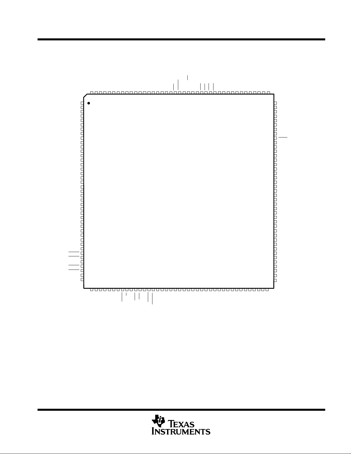
pinout
NC
NC
NC
A20
V
A19
A18
A17
DV
A16
A15
V
A14
A13
CV
A12
A11
DV
A10
V
DV
V
CV
DV
PAGE3
PAGE2
V
PAGE1
PAGE0
NC
NC
SM320VC33, SMJ320VC33
DIGITAL SIGNAL PROCESSOR
SGUS034E - FEBRUARY 2001 - REVISED OCTOBER 2002
SS
RESET
V
143
144
63
62
†‡
CV
MCBL/MP
EDGEMODE
140
141
142
66
65
64
DD
INT0
139
67
INT1
138
68
INT2
137
69
INT3
136
70
71
SS
V
135
XF0
134
72
73
XF1
133
74
DD
DV
132
131
75
SS
TCLK0
TCLK1DXCLKX0
FSX
V
127
128
129
130
80
79
78
77
76
126
NC
NC
125
124
NC
123
122
NC
121
NC
120
DV
DD
119
CLKR
118
FSR0
117
V
SS
116
DR0
115
TRST
114
TMS
113
CV
DD
112
TDI
111
TDO
110
TCK
109
V
SS
108
EMU0
107
EMU1
106
DV
DD
105
D0
104
D1
103
D2
102
D3
101
V
SS
100
D4
99
D5
98
DV
DD
97
D6
96
D7
95
CV
DD
94
D8
93
D9
92
V
SS
91
D10
90
D11
89
DV
DD
88
D12
87
D13
86
D14
85
D15
84
NC
83
NC
81
82
HFG PACKAGE
(TOP VIEW)
DD
DD
SS
163
43
162
44
A21
161
45
DV
160
46
A22
159
47
158
48
A23
157
49
V
RSV0
156
50
RSV1
155
51
NCNCNC
164
1
2
3
4
5
SS
6
7
8
9
DD
10
11
12
SS
13
14
15
DD
16
17
18
DD
19
A9
20
21
SS
A8
22
23
A7
24
A6
25
A5
26
DD
27
A4
28
SS
29
A3
30
A2
31
DD
32
A1
33
A0
34
DD
35
36
37
SS
38
39
40
41
42
DD
CV
154
52
CLKMD0
CLKMD1
152
153
54
53
PLLV
151
55
SS
XIN
150
56
XOUT
148
149
58
57
PLLV
EXTCLK
147
59
DV
146
60
DD
SHZ
145
61
H1
NC
DV
DD
H3
SS
DD
R/W
V
STRB
DV
IACK
RDY
CV
DD
HOLD
HOLDA
SS
D30
D31
D29
V
DV
DD
D28
D27
SS
D25
D24
D26
V
DV
DD
D23
D22
SS
DD
D21
D20
D19
CV
D18
V
DV
DD
D17
D16
SS
NC
NC
V
respectively.
SS,
NC
NC
NC - No internal connection
†
DVDD is the power supply for the I/O pins while CVDD is the power supply for the core CPU. VSS is the ground for both the I/O
pins and the core CPU.
‡
PLLVDD and PLLVSS are isolated PLL supply pins that should be externally connected to CVDD and V
The SM/SMJ320VC33 device is packaged in 164-pin low-profile quad flatpacks (HFG Suffix) and in 144-ball
fine pitch ball grid arrays (GNL and GNM Suffix).
POST OFFICE BOX 1443 • HOUSTON, TEXAS 77251-1443
3
Page 4
SM320VC33, SMJ320VC33
DV
DD
DV
DD
DIGITAL SIGNAL PROCESSOR
SGUS034E - FEBRUARY 2001 - REVISED OCTOBER 2002
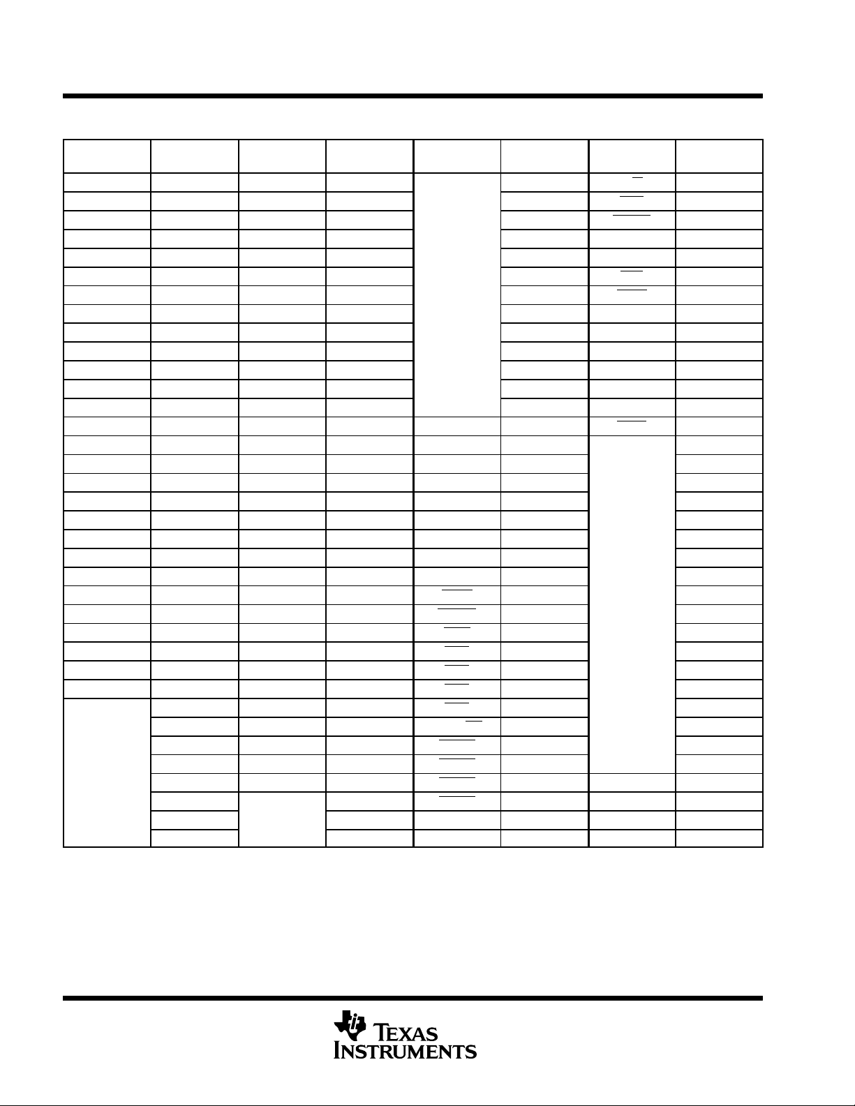
GNM Terminal Assignments† (Sorted by Signal Name)
SIGNAL
NAME
PIN
NUMBER
SIGNAL
NAME
PIN
NUMBER
SIGNAL
NAME
PIN
NUMBER
SIGNAL
NAME
PIN
NUMBER
A0 J2 D0 G12 M1 R/W L4
A1 K2 D1 G10 N1 RDY M5
A2 K1 D2 F13 N4 RESET B7
A3 J4 D3 G11 N7 RSV0 B4
A4 H4 D4 H10 M8 RSV1 D5
A5 H3 D5 H13 N12 SHZ D7
A6 H1 D6 H12
A7 G4 D7 J10
DV
DD
L13 STRB M4
H11 TCK F10
A8 G1 D8 J11 F11 TCLK0 C10
A9 G2 D9 J12 B12 TCLK1 A11
A10 F3 D10 K13 A10 TDI E11
A11 F4 D11 K12 A6 TDO D13
A12 F2 D12 K10 A1 TMS E10
A13 E1 D13 M13 DX0 A12 TRST C13
A14 E2 D14 L11 EDGEMODE A7 B1
A15 E4 D15 L12 EMU0 F12 D1
A16 C1 D16 M12 EMU1 E12 G3
A17 C2 D17 L10 EXTCLK C6 J1
A18 D3 D18 K9 FSR0 C12 L2
A19 C3 D19 N11 FSX D10 M3
A20 B2 D20 M11 H1 L3 M6
A21 D4 D21 M10 H3 N2 L7
A22 A2 D22 K8 HOLD N5
A23 B3 D23 N9 HOLDA K5
V
SS
N10
N13
CLKMD0 C5 D24 M9 IACK K4 K11
CLKMD1 B5 D25 L8 INT0 C8 G13
CLKR0 B13 D26 N8 INT1 B9 E13
CLKX0 B11 D27 M7 INT2 D8 A13
E3 D28 K7 INT3 A9 C11
J3 D29 L6 MCBL/MP B8 C9
L5 D30 N6 PAGE0 M2 C7
CV
DD
L9 D31 K6 PAGE1 N3 C4
J13 DR0 D11 PAGE2 L1 XF0 B10
D12 D2 PAGE3 K3 XF1 D9
A8
DV
DD
A3
†
DVDD is the power supply for the I/O pins while CVDD is the power supply for the core CPU. VSS is the ground for both the I/O pins and the core
CPU.
‡
PLLVDD and PLLVSS are isolated PLL supply pins that should be externally connected to CVDD and V
F1 PLLV
H2 PLLV
DD
SS
‡
‡
A5 XIN B6
A4 XOUT D6
respectively.
SS,
4
POST OFFICE BOX 1443 • HOUSTON, TEXAS 77251-1443
Page 5
SM320VC33, SMJ320VC33
DIGITAL SIGNAL PROCESSOR
SGUS034E - FEBRUARY 2001 - REVISED OCTOBER 2002
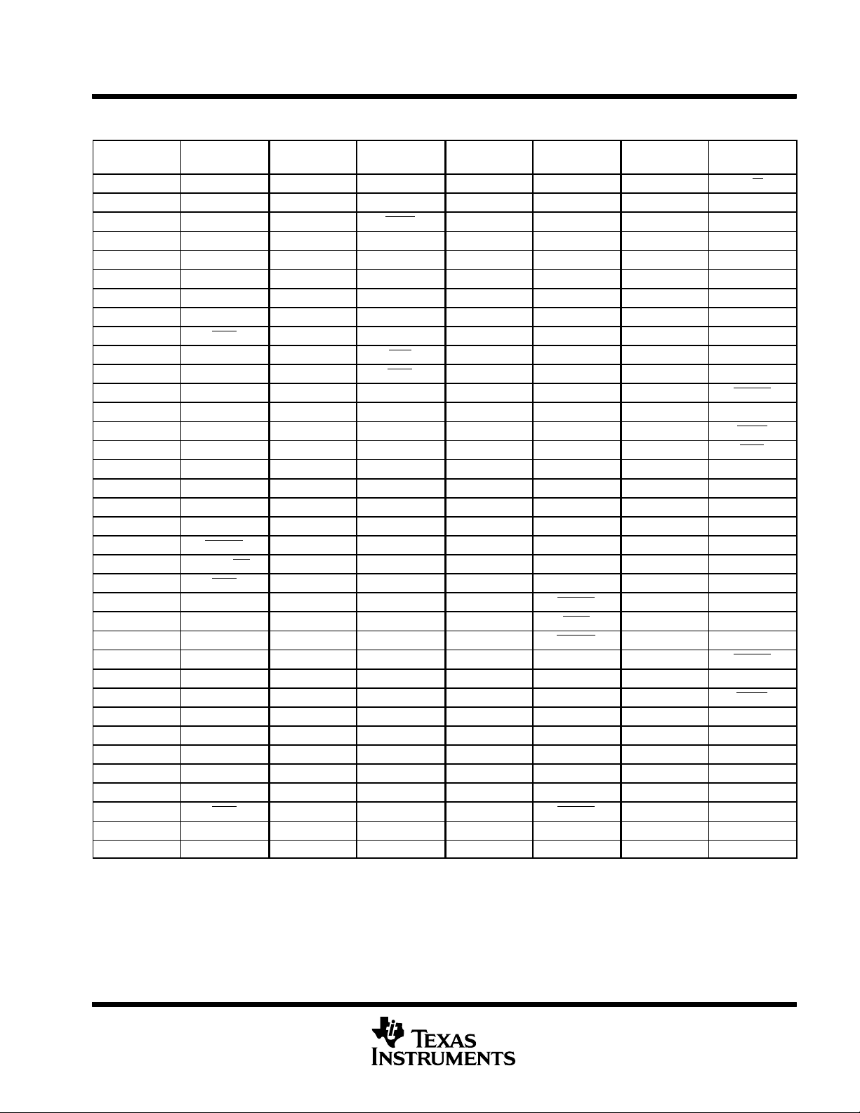
GNM Terminal Assignments† (Sorted by Pin Number)
PIN
NUMBER
A1 DV
A2 A22 C12 FSR0 G11 D3 L5 CV
A3 CV
A4 PLLV
A5 PLLV
A6 DV
SIGNAL
NAME
DD
DD
SS
DD
DD
PIN
NUMBER
C11 V
SIGNAL
NAME
SS
PIN
NUMBER
SIGNAL
NAME
PIN
NUMBER
G10 D1 L4 R/W
C13 TRST G12 D0 L6 D29
D1 V
D2 DV
SS
DD
D3 A18 H2 DV
G13 V
SS
L7 V
H1 A6 L8 D25
DD
L9 CV
SIGNAL
NAME
DD
SS
DD
A7 EDGEMODE D4 A21 H3 A5 L10 D17
A8 CV
DD
D5 RSV1 H4 A4 L11 D14
A9 INT3 D6 XOUT H10 D4 L12 D15
A10 DV
DD
A11 TCLK1 D8 INT2 H12 D6 M1 DV
D7 SHZ H11 DV
DD
L13 DV
DD
DD
A12 DX D9 XF1 H13 D5 M2 PAGE0
A13 V
B1 V
SS
SS
B2 A20 D12 CV
B3 A23 D13 TDO J4 A3 M6 V
D10 FSX J1 V
SS
M3 V
SS
D11 DR0 J2 A0 M4 STRB
DD
J3 CV
DD
M5 RDY
SS
B4 RSV0 E1 A13 J10 D7 M7 D27
B5 CLKMD1 E2 A14 J11 D8 M8 DV
B6 XIN E3 CV
DD
B7 RESET E4 A15 J13 CV
J12 D9 M9 D24
DD
M10 D21
DD
B8 MCBL/MP E10 TMS K1 A2 M11 D20
B9 INT1 E11 TDI K2 A1 M12 D16
B10 XF0 E12 EMU1 K3 PAGE3 M13 D13
B11 CLKX0 E13 V
B12 DV
DD
F1 DV
SS
DD
K4 IACK N1 DV
K5 HOLDA N2 H3
DD
B13 CLKR F2 A12 K6 D31 N3 PAGE1
C1 A16 F3 A10 K7 D28 N4 DV
DD
C2 A17 F4 A11 K8 D22 N5 HOLD
C3 A19 F10 TCK K9 D18 N6 D30
C4 V
SS
C5 CLKMD0 F12 EMU0 K11 V
F11 DV
DD
K10 D12 N7 DV
SS
N8 D26
DD
C6 EXTCLK F13 D2 K12 D11 N9 D23
C7 V
SS
G1 A8 K13 D10 N10 V
SS
C8 INT0 G2 A9 L1 PAGE2 N11 D19
C9 V
SS
C10 TCLK0 G4 A7 L3 H1 N13 V
†
DVDD is the power supply for the I/O pins while CVDD is the power supply for the core CPU. VSS is the ground for both the I/O pins and the core
CPU.
‡
PLLVDD and PLLVSS are isolated PLL supply pins that should be externally connected to CVDD and V
G3 V
SS
L2 V
SS
respectively.
SS,
N12 DV
DD
SS
POST OFFICE BOX 1443 • HOUSTON, TEXAS 77251-1443
5
Page 6
SM320VC33, SMJ320VC33
†
DESCRIPTION
DIGITAL SIGNAL PROCESSOR
SGUS034E - FEBRUARY 2001 - REVISED OCTOBER 2002
Terminal Functions
TERMINAL
NAME QTY
D31- D0 32 I/O/Z
A23- A0 24 O/Z 24-bit address port S H R
R/W 1 O/Z
STRB 1 O/Z Strobe. For all external-accesses S H
PAGE0 PAGE3
RDY 1 I
HOLD 1 I
HOLDA 1 O/Z
RESET 1 I
EDGEMODE 1 I Edge mode. Enables interrupt edge mode detection.
INT3- INT0 4 I External interrupts
IACK 1 O/Z
MCBL/MP 1 I Microcomputer Bootloader/microprocessor mode-select
SHZ 1 I
XF1, XF0 2 I/O/Z
CLKR0 1 I/O/Z Serial port 0 receive clock. CLKR0 is the serial shift clock for the serial port 0 receiver. S R
CLKX0 1 I/O/Z
DR0 1 I/O/Z Data-receive. Serial port 0 receives serial data on DR0. S R
DX0 1 I/O/Z Data-transmit output. Serial port 0 transmits serial data on DX0. S R
FSR0 1 I/O/Z
FSX0 1 I/O/Z
†
I = input, O = output, Z = high-impedance state
‡
S = SHZ active, H = HOLD active, R = RESET active
§
Recommended decoupling. Four 0.1 µF for CVDD and eight 0.1 µF for DVDD.
TYPE
PRIMARY-BUS INTERFACE
32-bit data port S H R
Data port bus keepers. (See Figure 9) S
Read/write. R/W is high when a read is performed and low when a write is performed
over the parallel interface.
1 O/Z Page strobes. Four decoded page strobes for external access S H R
Ready. RDY indicates that the external device is prepared for a transaction
completion.
Hold. When HOLD is a logic low, any ongoing transaction is completed. A23- A0,
D31-D0, STRB, and R/W are placed in the high-impedance state and all
transactions over the primary-bus interface are held until HOLD becomes a logic high
or until the NOHOLD bit of the primary-bus-control register is set.
Hold acknowledge. HOLDA is generated in response to a logic-low on HOLD.
HOLDA indicates that A23-A0, D31-D0, STRB, and R/W are in the high-impedance
state and that all transactions over the bus are held. HOLDA is high in response to
a logic-high of HOLD or the NOHOLD bit of the primary-bus-control register is set.
CONTROL SIGNALS
Reset. When RESET is a logic low, the device is in the reset condition. When RESET
becomes a logic high, execution begins from the location specified by the reset vector.
Internal acknowledge. IACK is generated by the IACK instruction. IACK can be used
to indicate when a section of code is being executed.
Shutdown high impedance. When active, SHZ places all pins in the high-impedance
state. SHZ can be used for board-level testing or to ensure that no dual-drive
conditions occur. CAUTION: A low on SHZ corrupts the device memory and register
contents. Reset the device with SHZ high to restore it to a known operating condition.
External flags. XF1 and XF0 are used as general-purpose I/Os or to support
interlocked processor instruction.
SERIAL PORT 0 SIGNALS
Serial port 0 transmit clock. CLKX0 is the serial shift clock for the serial port 0
transmitter.
Frame-synchronization pulse for receive. The FSR0 pulse initiates the data-receive
process using DR0.
Frame-synchronization pulse for transmit. The FSX0 pulse initiates the data-transmit
process using DX0.
CONDITIONS
WHEN
SIGNAL IS Z TYPE
S H R
S
S
S R
S R
S R
S R
‡
6
POST OFFICE BOX 1443 • HOUSTON, TEXAS 77251-1443
Page 7
SGUS034E - FEBRUARY 2001 - REVISED OCTOBER 2002
†
DESCRIPTION
Terminal Functions (Continued)
SM320VC33, SMJ320VC33
DIGITAL SIGNAL PROCESSOR
TERMINAL
NAME QTY
TYPE
TIMER SIGNALS
TCLK0 1 I/O/Z
TCLK1 1 I/O/Z
Timer clock 0. As an input, TCLK0 is used by timer 0 to count external pulses. As
an output, TCLK0 outputs pulses generated by timer 0.
Timer clock 1. As an input, TCLK1 is used by timer 1 to count external pulses. As
an output, TCLK1 outputs pulses generated by timer 1.
SUPPLY AND OSCILLATOR SIGNALS
H1 1 O/Z External H1 clock S
H3 1 O/Z External H3 clock S
CV
DV
V
SS
PLLV
PLLV
DD
DD
DD
SS
8 I
16 I
18 I Ground. All grounds must be connected to a common ground plane.
1 I Internally isolated PLL supply. Connect to CVDD (1.8 V)
1 I Internally isolated PLL ground. Connect to V
EXTCLK 1 I
XOUT 1 O
XIN 1 I
CLKMD0,
CLKMD1
2 I Clock mode select pins
+VDD. Dedicated 1.8-V power supply for the core CPU. All must be connected to
a common supply plane.
+VDD. Dedicated 3.3-V power supply for the I/O pins. All must be connected to a
common supply plane.
§
§
SS
External clock. Logic level compatible clock input. If the XIN/XOUT oscillator is
used, tie this pin to ground.
Clock out. Output from the internal-crystal oscillator. If a crystal is not used, XOUT
should be left unconnected.
Clock in. Internal-oscillator input from a crystal. If EXTCLK is used, tie this pin to
ground.
RSV0 - RSV1 2 I Reserved. Use individual pullups to DVDD.
JTAG EMULATION
EMU1- EMU0 2 I/O Emulation pins 0 and 1, use individual pullups to DV
DD
TDI 1 I Test data input
TDO 1 O Test data output
TCK 1 I Test clock
TMS 1 I Test mode select
TRST 1 I Test reset
†
I = input, O = output, Z = high-impedance state
‡
S = SHZ active, H = HOLD active, R = RESET active
§
Recommended decoupling. Four 0.1 µF for CVDD and eight 0.1 µF for DVDD.
CONDITIONS
WHEN
SIGNAL IS Z TYPE
S R
S R
‡
POST OFFICE BOX 1443 • HOUSTON, TEXAS 77251-1443
7
Page 8
SM320VC33, SMJ320VC33
DIGITAL SIGNAL PROCESSOR
SGUS034E - FEBRUARY 2001 - REVISED OCTOBER 2002
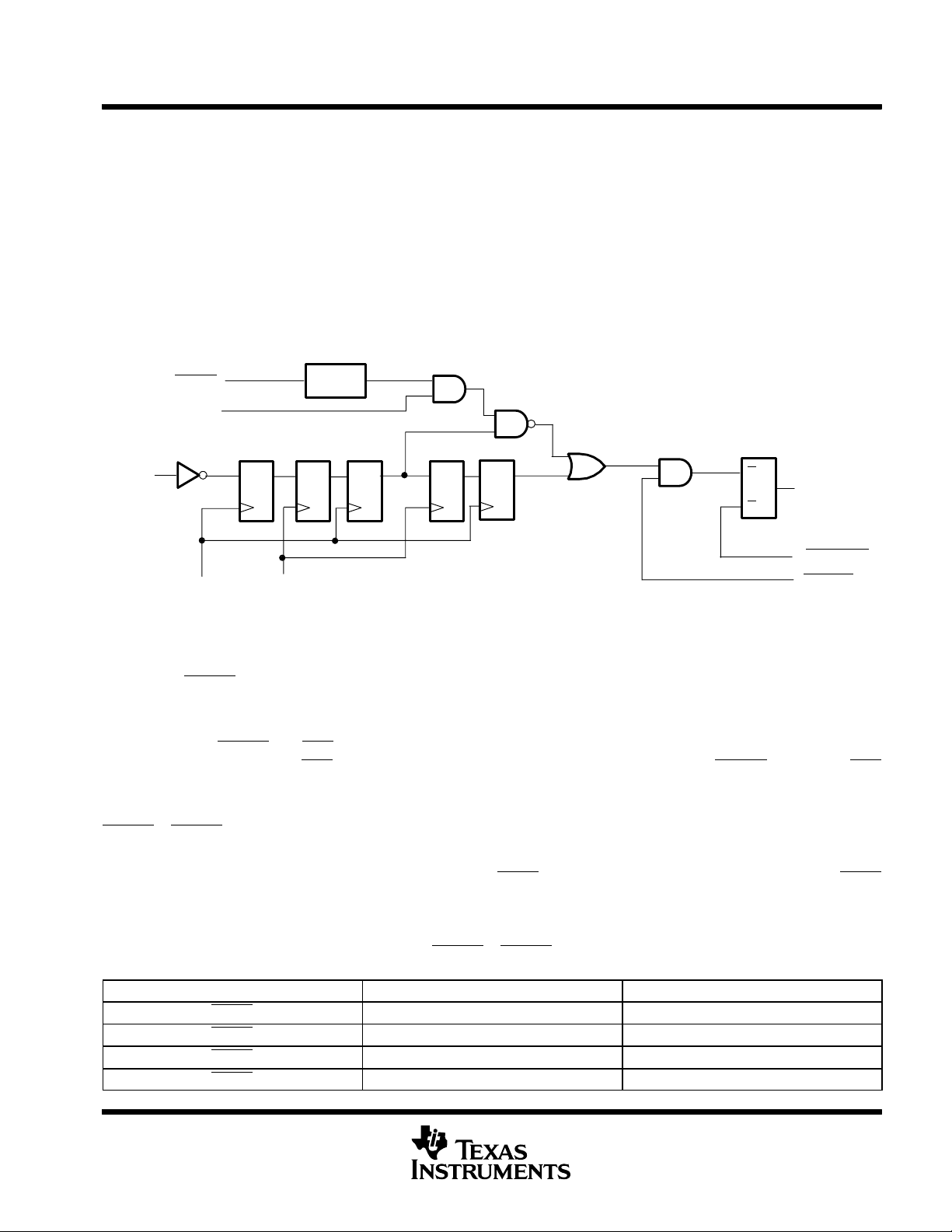
functional block diagram
PAGE0
PAGE1
PAGE2
PAGE3
RDY
HOLD
HOLDA
STRB
R/W
D31- D0
A23- A0
RSV(0,1)
SHZ
EDGEMODE
RESET
INT(3- 0)
IACK
MCBL/MP
XF(1,0)
TDI
TDO
EMU0
EMU1
TCK
TMS
TRST
EXTCLK
XOUT
XIN
CLKMD(0,1)
MUX
RAM
Block 0
(1K × 32)
24
32 32 40 40
REG1
REG2
Multiplier
40
40
40
32
24
24
32
32
32
32
Cache
(64 × 32)
32 24 24
PDATA Bus
PADDR Bus
DDATA Bus
DADDR1 Bus
MUX
DADDR2 Bus
DMADATA Bus
DMAADDR Bus
IR
PC
Controller
JTAG Emulation
H1
H3
PLL CLK
32
CPU1
RAM
Block 1
(1K × 32)
24 2432 32 32
24
32
CPU1
CPU2
REG1
REG2
ARAU0 ARAU1
24
32-Bit
Barrel
Shifter
ALU
Extended-
Precision
Registers
(R7-R0)
DISP0, IR0, IR1
BK
Auxiliary
Registers
(AR0- AR7)
Other
Registers
(12)
24
32
DMA Controller
Global-Control
Source-Address
Destination-
40
40
24
32
32
Boot
Loader
Register
Register
Address
Register
Transfer-
Counter
Register
40
RAM
Block 2
(16K × 32)
24
24
32
Peripheral Data Bus
FSX0
DX0
CLKX0
FSR0
DR0
CLKR0
TCLK0
TCLK1
RAM
Block 3
(16K × 32)
24
32
Serial Port 0
Serial-Port-Control
Register
Receive/Transmit
(R/X) Timer Register
Data-Transmit
Register
Data-Receive
Register
Timer 0
Global-Control
Register
Timer-Period
Register
Timer-Counter
Register
Timer 1
Global-Control
Register
Timer-Period
Register
Timer-Counter
Register
Port Control
STRB-Control
Register
MUX
Peripheral Data Bus
Peripheral Address Bus
8
POST OFFICE BOX 1443 • HOUSTON, TEXAS 77251-1443
Page 9
memory map
SM320VC33, SMJ320VC33
DIGITAL SIGNAL PROCESSOR
SGUS034E - FEBRUARY 2001 - REVISED OCTOBER 2002
0h
03Fh
040h
7FFFFFh
800000h
803FFFh
804000h
807FFFh
808000h
8097FFh
809800h
809BFFh
809C00h
809FFFh
80A000h
FFFFFFh
Reset, Interrupt, Trap V ector, and
Reserved Locations (64)
(External STRB
STRB
(8M Words - 64 Words)
RAM Block 2
(16K Words Internal)
RAM Block 3
(16K Words Internal)
Peripheral Bus
Memory-Mapped Registers
(6K Words Internal)
RAM Block 0
(1K Words Internal)
RAM Block 1
(1K Words Internal)
STRB
(8M Words - 40K Words)
(a) Microprocessor Mode
External
Active
External
Active
Active)
0h
FFFh
1000h
400000h
7FFFFFh
800000h
803FFFh
804000h
807FFFh
808000h
8097FFh
809800h
809BFFh
809C00h
809FC0h
809FC1h
809FFFh
80A000h
FFF000h
FFFFFFh
Reserved for Bootloader
Operations
Boot 1
External
STRB
Active
Boot 2
(16K Words Internal)
(16K Words Internal)
Memory-Mapped Registers
(6K Words Internal)
(1K Words Internal)
(1K Words Internal)
User-Program Interrupt
and Trap Branch Table
63 Words
Boot 3
(b) Microcomputer/Bootloader Mode
(8M Words -
4K Words)
RAM Block 2
RAM Block 3
Peripheral Bus
RAM Block 0
RAM Block 1
External
STRB
(8M Words -
40K Words)
Active
NOTE A: STRB is active over all external memory ranges. PAGE0 to PAGE3 are configured as external bus strobes. These are simple
decoded strobes that have no configuration registers and are active only during external bus activity over the following ranges:
Name Active range
PAGE0 0000000h – 03FFFFFh
PAGE1 0400000h – 07FFFFFh
PAGE2 0800000h – 0BFFFFFh
PAGE3 0C00000h – 0FFFFFFh
STRB 0000000h – 0FFFFFFh
Figure 1. SM/SMJ320VC33 Memory Maps
POST OFFICE BOX 1443 • HOUSTON, TEXAS 77251-1443
9
Page 10
SM320VC33, SMJ320VC33
DIGITAL SIGNAL PROCESSOR
SGUS034E - FEBRUARY 2001 - REVISED OCTOBER 2002
memory map (continued)
00h
01h
02h
03h
04h
05h
06h
07h
08h
09h
0Ah
0Bh
0Ch
1Fh
Reset
INT0
INT1
INT2
INT3
XINT0
RINT0
Reserved
TINT0
TINT1
DINT
Reserved
TRAP 020h
809FC1h
809FC2h
809FC3h
809FC4h
809FC5h
809FC6h
809FC7h
809FC8h
809FC9h
809FCAh
809FCBh
809FCCh
809FDFh
809FE0h
INT0
INT1
INT2
INT3
XINT0
RINT0
Reserved
TINT0
TINT1
DINT
Reserved
TRAP 0
3Ch
3Fh
TRAP 273Bh 809FFBh
Reserved
(a) Microprocessor Mode (b) Microcomputer / Bootloader Mode
809FFCh
809FFFh
TRAP 27
Reserved
Figure 2. Reset, Interrupt, and Trap Vector/Branches Memory-Map Locations
10
POST OFFICE BOX 1443 • HOUSTON, TEXAS 77251-1443
Page 11
memory map (continued)
SM320VC33, SMJ320VC33
DIGITAL SIGNAL PROCESSOR
SGUS034E - FEBRUARY 2001 - REVISED OCTOBER 2002
808000h
808004h
808006h
808008h
808020h
808024h
808028h
808030h
808034h
808038h
808040h
808042h
808043h
808044h
808045h
808046h
DMA Global Control
DMA Source Address
DMA Destination Address
DMA Transfer Counter
Timer 0 Global Control
Timer 0 Counter
Timer 0 Period Register
Timer 1 Global Control
Timer 1 Counter
Timer 1 Period Register
Serial Global Control
FSX/DX/CLKX Serial Port Control
FSR/DR/CLKR Serial Port Control
Serial R/X Timer Control
Serial R/X Timer Counter
Serial R/X Timer Period Register
808048h
80804Ch
808064h
NOTE A: Shading denotes reserved address locations.
Data-Transmit
Data-Receive
Primary-Bus Control
Figure 3. Peripheral Bus Memory-Mapped Registers
clock generator
The clock generator provides clocks to the VC33 device, and consists of an internal oscillator and a
phase-locked loop (PLL) circuit. The clock generator requires a reference clock input, which can be provided
by using a crystal resonator with the internal oscillator, or from an external clock source. The PLL circuit
generates the device clock by multiplying the reference clock frequency by a x5 scale factor, allowing use of
a clock source with a lower frequency than that of the CPU. The PLL is an adaptive circuit that, once
synchronized, locks onto and tracks an input clock signal.
POST OFFICE BOX 1443 • HOUSTON, TEXAS 77251-1443
11
Page 12
SM320VC33, SMJ320VC33
DIGITAL SIGNAL PROCESSOR
SGUS034E - FEBRUARY 2001 - REVISED OCTOBER 2002
PLL and clock oscillator control
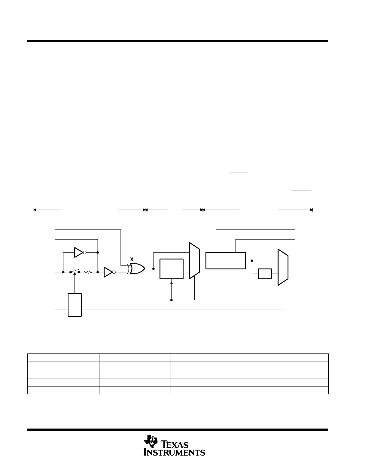
The clock mode control pins are decoded into four operational modes as shown in Figure 4. These modes
control clock divide ratios, oscillator, and PLL power (see Table 2).
When an external clock input or crystal is connected, the opposite unused input is simply grounded. An XOR
gate then passes one of the two signal sources to the PLL stage. This allows the direct injection of a clock
reference into EXTCLK, or 1-20 MHz crystals and ceramic resonators with the oscillator circuit. The two clock
sources include:
D A crystal oscillator circuit, where a crystal or ceramic resonator is connected across the XOUT and XIN pins
and EXTCLK is grounded.
D An external clock input, where an external clock source is directly connected to the EXTCLK pin, and XOUT
is left unconnected and XIN is grounded.
When the PLL is initially started, it enters a transitional mode during which the PLL acquires lock with the input
signal. Once the PLL is locked, it continues to track and maintain synchronization with the input signal. The PLL
is a simple x5 reference multiplier with bypass and power control.
The clock divider, under CPU control, reduces the clock reference by 1 (MAXSPEED), 1/16 (LOWPOWER), or
clock stop (IDLE2). Wake-up from the IDLE2 state is accomplished by a RESET or interrupt pin logic-low state.
A divide-by-two TMS320C31 equivalent mode of operation is also provided. In this case, the clock output
reference is further divided by two with clock synchronization being determined by the timing of RESET falling
relative to the present H1/H3 state.
Clock DividerPLLClock & Crystal OSC
EXTCLK
XOUT
M
U
X
X1, 1/16, Off
C31 DIV2 Mode
1/2
M
U
X
XIN
CLKMD0
CLKMD1
RFS1
Oscillator Enable
SEL
XOR
PLLX5
PLL PWR and Bypass
Figure 4. Clock Generation
T able 2. Clock Mode Select Pins
CLKMD0 CLKMD1 FEEDBACK PLLPWR RATIO NOTES
0 0 Off Off 1 Fully static, very low power
0 1 On Off 1/2 Oscillator enabled
1 0 On Off 1 Oscillator enabled
1 1 On On 5 2 mA @ 60 MHz, 1.8 V PLL power. Oscillator enabled
MAXSPEED/
LOWPOWER
IDLE2
CPU CLOCK
12
POST OFFICE BOX 1443 • HOUSTON, TEXAS 77251-1443
Page 13
SM320VC33, SMJ320VC33
DIGITAL SIGNAL PROCESSOR
SGUS034E - FEBRUARY 2001 - REVISED OCTOBER 2002
PLL and clock oscillator control (continued)
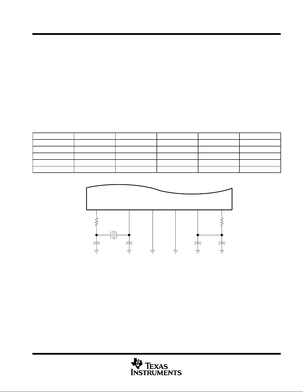
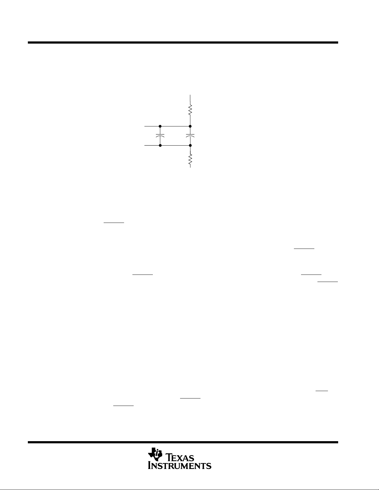
Typical crystals in the 8-30 MHz range have a series resistance of 25 Ω, which increases below 8 MHz. To
maintain proper filtering and phase relationships, Rd and Z
the crystal. A series compensation resistor (Rd), shown in Figure 5, is recommended when using lower
frequency crystals. The XOUT output, the square wave inverse of XIN, is then filtered by the XOUT output
impedance, C1 load capacitor, and Rd (if present). The crystal and C2 input load capacitor then refilters this
signal, resulting in a XIN signal that is 75-85% of the oscillator supply voltage.
NOTE: Some ceramic resonators are available in a low-cost, three-terminal package that includes C1 and C2
internally. Typically, ceramic resonators do not provide the frequency accuracy of crystals.
NOTE: Better PLL stability can be achieved using the optional power supply isolation circuit shown in Figure 5.
A similar filter can be used to isolate the PLLVSS, as shown in Figure 6. PLL VDD can also be directly connected
DD
.
to CV
Table 3. Typical Crystal Circuit Loading
FREQUENCY (MHz) Rd (Ω) C1 (pF) C2 (pF) CL† (pF) RL† (Ω)
2 4.7k 18 18 12 200
5 2.2k 18 18 12 60
10 470 15 15 12 30
15 0 15 12 12 25
†
CL and RL are typical internal series load capacitance and resistance of the crystal.
20 0 9 9 10 25
of the oscillator circuit should be 10x-40x that of
out
XOUT XIN
Crystal
C1 C2
Figure 5. Self-Oscillation Mode
EXTCLKRdPLLV
SS
PLLV
DD
0.1 µF
100 Ω
CV
DD
0.01 µF
POST OFFICE BOX 1443 • HOUSTON, TEXAS 77251-1443
13
Page 14
SM320VC33, SMJ320VC33
DIGITAL SIGNAL PROCESSOR
SGUS034E - FEBRUARY 2001 - REVISED OCTOBER 2002
PLL isolation
The internal PLL supplies can be directly connected to CVDD and VSS (0 Ω case) or fully isolated as shown in
Figure 6. The RC network prevents the PLL supplies from turning high frequency noise in the CVDD and V
supplies into jitter.
CV
DD
0 -100 Ω
PLLV
DD
0.1 µF
PLLV
SS
Figure 6. PLL Isolation Circuit Diagram
V
SS
0.01 µF
0 -100 Ω
SS
clock and PLL considerations on initialization
On power up, the CPU clock divide mode can be in MAXSPEED, LOPOWER or IDLE2, or the PLL could be
in an undefined mode. RESET falling in the presence of a valid CPU clock is used to clear this state, after which
the device will synchronously terminate any external activity.
The 5x Fclkin PLL of the 320VC33 contains an 8-bit PLL-LOCK counter that will cause the PLL to output a
frequency of Fclkin/2 during the initial ramp. This counter, however, does not increment while RESET is low or
in the absence of an input clock. A minimum of 256 input clocks are required before the first falling edge of reset
for the PLL to output to clear this counter. The setup and behavior that is seen is as follows.
Power is applied to the DSP with RESET low and the input clock high or low. A clock is applied (RESET is still
low) and the PLL appears to lock on to the input clock, producing the expected x5 output frequency. RESET
is driven high and the PLL output immediately drops to Fclkin/2 for up to 256 input cycles or 128 of the Fclkin/2
output cycles. The PLL/CPU clock then switches to x5 mode.
The switch over is synchronous and does not create a clock glitch, so the only effect is that the CPU will run
slow for up to the first 128 cycles after reset goes high. Once the PLL has stabilized, the counter will remain
cleared and subsequent resets will not exhibit this condition.
power sequencing considerations
Though an internal ESD and CMOS latchup protection diode exists between CVDD and DVDD, it should not be
considered a current-carrying device on power up. An external Schottky diode should be used to prevent CV
from exceeding DVDD by more than 0.7 V. The effect of this diode during power up is that if CVDD is powered
up first, DVDD will follow by one diode drop even when the DVDD supply is not active.
DD
Typical s y s tems using LDOs of the same family type for both DVDD and CVDD will track each other during power
up. In most cases, this is acceptable; but if a high-impedance pin state is required on power up, the SHZ pin
can be used to asynchronously disable all outputs. RESET should not be used in this case since some signals
require an active clock for RESET to have an effect and the clock may not yet be active. The internal core logic
becomes functional at approximately 0.8 V while the external pin IO becomes active at about 1.5 V.
14
POST OFFICE BOX 1443 • HOUSTON, TEXAS 77251-1443
Page 15
SM320VC33, SMJ320VC33
DIGITAL SIGNAL PROCESSOR
SGUS034E - FEBRUARY 2001 - REVISED OCTOBER 2002
EDGEMODE
When EDGEMODE = 1, a sampled digital delay line is decoded to generate a pulse on the falling edge of the
interrupt pin. To ensure interrupt recognition, input signal logic-high and logic-low states must be held longer
than the synchronizer delay of one CPU clock cycle. Holding these inputs to no less than two cycles in both the
logic-low and logic-high states is sufficient.
When EDGEMODE = 0, a logic-low interrupt pin will continually set the corresponding interrupt flag. The CPU
or DMA can clear this flag within two cycles of it being set. This is the maximum interrupt width that can be applied
if only one interrupt is to be recognized. The CPU can manually clear IF bits within an interrupt service routine
(ISR), effectively lengthening the maximum ISR width.
After reset, EDGEMODE is temporarily disabled, allowing logic-low INT pins to be detected for bootload
operation.
Delay
DQ DQ
H3
DQ
S
Q
R
EDGEMODE
INTn
RESET
DDQQ
H1
Figure 7. EDGEMODE and Interrupt Flag CIrcuit
reset operation
When RESET is applied, the CPU attempts to safely exit any pending read or write operations that may be in
progress. This can take as much as 10 CPU cycles, after which, the address, data, and control pins will be in
an inactive or high-impedance state.
When both RESET and SHZ are applied, the device will immediately enter the reset state with the pins held in
high-impedance mode. SHZ should then be disabled at least 10 CPU cycles before RESET is set high. SHZ
can be used during power-up sequencing to prevent undefined address, data, and control pins, avoiding system
conflicts.
IF Bit
CPU Reset
CPU Set
PAGE0 - PAGE3 select lines
To facilitate simpler and higher speed connection to external devices, the SM/SMJ320VC33 includes four
predecoded select pins that have the same timings as STRB. These pins are decoded from A22, A23, and STRB
and are active only during external accesses over the ranges shown in Table 4. All external bus accesses are
controlled by a single bus control register.
T able 4. PAGE0 - PAGE3 Ranges
START END
PAGE0 0x000000 0x3FFFFF
PAGE1 0x400000 0x7FFFFF
PAGE2 0x800000 0xBFFFFF
PAGE3 0xC00000 0xFFFFFF
POST OFFICE BOX 1443 • HOUSTON, TEXAS 77251-1443
15
Page 16
SM320VC33, SMJ320VC33
DIGITAL SIGNAL PROCESSOR
SGUS034E - FEBRUARY 2001 - REVISED OCTOBER 2002
using external logic with the READY pin
The key to designing external wait-state logic is the internal bus control register and associated internal logic
that logically combines the external READY pin with the much faster on-chip bus control logic. This essentially
allows slow external logic to interact with the bus while easily meeting the READY input timings. It is also relevant
to mention that the combined ready signals are sampled on the rising edge of the internal H1 clock. Please refer
to Figure 8 for the following examples.
example 1
A simple 0 or WTCNT wait-state decoder can be created by simply tying an address line back to the READY
pin and selecting the AND option. When the tied back address is low, the bus will run with 0 wait states. When
the tied back address is high, the bus will be controlled by the internal wait-state counter .
By enabling the bank compare logic, proper operation is further ensured by inserting a null cycle before a read
on the next bank is performed (writes are not pre-extended). This extra time can also be used by external logic
to affect the feedback path.
example 2
An N-WTCNT minimum wait-state decoder can also be created by tying back an address line to READY and
logically ORing it with the internal bank compare and wait count signals. When the address pin is low, bus timing
is determined by the internal WTCNT and BNKCMP settings. When the address line is high, the bus can run
no faster than the WTCNT counter and will be extended as long as READY is held high.
Bus_Enable_Strobe,
0 = Active
BUS_READY
External Bus Interface
Q
H1
Abus_old
H3
1
2
3
0
PAGE_0
PAGE_1
PAGE_2
PAGE_3
Device
Enable
Pins
R
N_Wait
Counter
A23
A22
0 = Bus Idle To C31 Style
Abus
D
Decode
H3
D Q
N-Bit
Bank
Compare
STRB Pin
Decoder
(C31 Compatibility)
READY Pin
16
R/W
Figure 8. Internal Ready Logic, Simplified Diagram
POST OFFICE BOX 1443 • HOUSTON, TEXAS 77251-1443
R/W Pin
Page 17
SM320VC33, SMJ320VC33
DIGITAL SIGNAL PROCESSOR
SGUS034E - FEBRUARY 2001 - REVISED OCTOBER 2002
example 2 (continued)
Table 5. MUX Select (Bus Control Register Bits 4 and 3)
BIT 4 BIT 3 RESULTS
0 0 Ignore internal wait counter and use only external READY
0 1 Use only internal wait counter and ignore ready pin
1 0 Logically AND internal wait counter with ready pin
1 1 Logically OR internal wait counter with ready pin (reset default)
posted writes
External writes are effectively “posted” to the bus, which then acts like an output latch until the write completes.
Therefore, if the application code is executing internally, it can perform a very slow external write with no penalty
since the bus acts like it has a one-level-deep write FIFO.
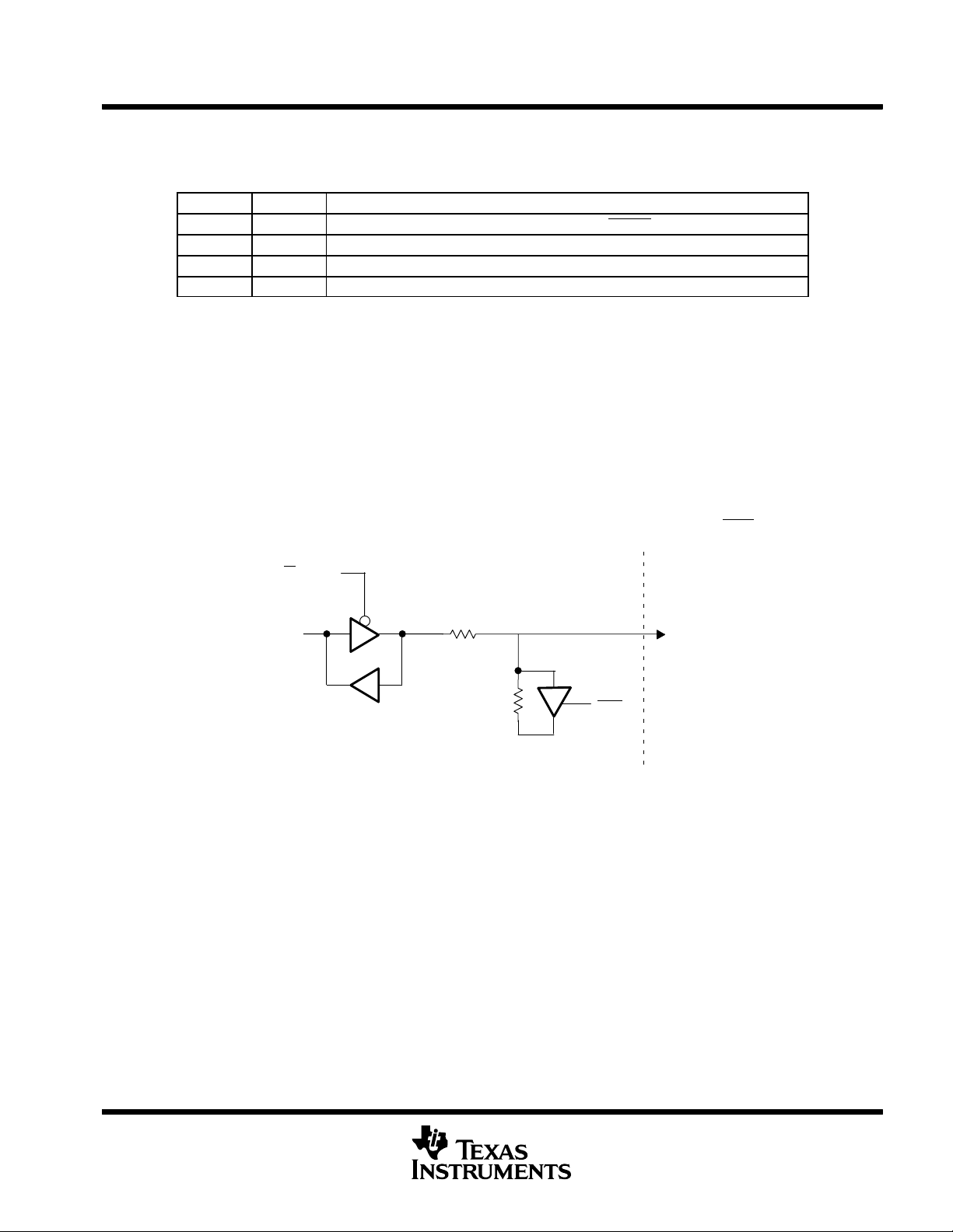
data bus I/O buffer
The circuit shown in Figure 9 is incorporated into each data pin to lightly “hold” the last driven value on the data
bus pins when the DSP or an external device is not actively driving the bus. Each bus keeper is built from a
three-state driver with nominal 15 kΩ output resistance which is fed back to the input in a positive feedback
configuration. The resistance isolated driver then pulls the output in one direction or the other keeping the last
driven value. This circuit is enabled in all functional modes and is only disabled when SHZ is pulled low.
R/W
Internal
Data Bus
30 Ω
15 kΩ
SHZ
Bus keeper
External Data
Bus Pin
Figure 9. Bus Keeper Circuit
For an external device to change the state of these pins, it must be able to drive a small dc current until the driver
threshold is crossed. At the crossover point, the driver changes state, agreeing with the external driver and
assisting the change. The voltage threshold of the bus keeper is approximately at 50% of the DVDD supply
voltage. The typical output impedance of 30 Ω for all SM/SMJ320VC33 I/O pins is easily capable of meeting
this requirement.
POST OFFICE BOX 1443 • HOUSTON, TEXAS 77251-1443
17
Page 18
SM320VC33, SMJ320VC33
DIGITAL SIGNAL PROCESSOR
SGUS034E - FEBRUARY 2001 - REVISED OCTOBER 2002
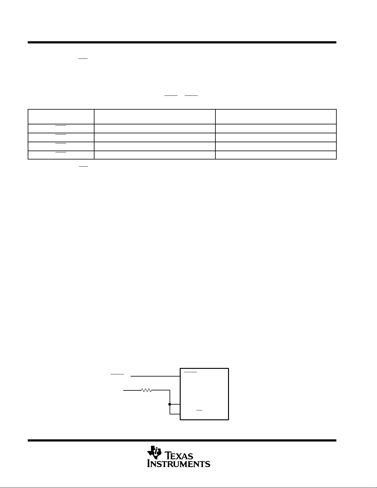
bootloader operation
When MCBL/MP = 1, an internal ROM is decoded into the address range of 0x000000-0x000FFF. Therefore,
when reset occurs, execution begins within the internal ROM program and vector space. No external activity
will be e v i dent until one of the boot options is enabled. These options are enabled by pulling an external interrupt
pin low, which the boot-load software then detects, causing a particular routine to be executed (see Table 6).
T able 6. INT0 - INT3 Sources
ACTIVE INTERRUPT
INT0 0x001000 8, 16, or 32-bit width
INT1 0x400000 8, 16, or 32-bit width
INT2 0xFFF000 8, 16, or 32-bit width
INT3 Serial Port 32-bit, external clock, and frame synch
ADDRESS/SOURCE WHERE BOOT DATA IS
READ FROM
DATA FORMAT
When MCBL/MP = 1, the reset and interrupt vectors are hard-coded within the internal ROM. Since this is a
read-only device, these vectors cannot be modified. To enable user-defined interrupt routines, the internal
vectors contain fixed values that point to an internal section of SRAM beginning at 0x809FC1. Code execution
begins at these locations so it is important to place branch instructions (to the interrupt routine) at these locations
and not vectors.
The bootloader program requires a small stack space for calls and returns. Two SRAM locations at 0x809800
and 0x809801 are used for this stack. Data should not be boot loaded into these locations as this will corrupt
the bootloader program run-time stack. After the boot-load operation is complete, a program can reclaim these
locations. The simplest solution is to begin a program stack or uninitialized data section at 0x809800.
For additional detail on bootloader operation including the bootloader source code, see the TMS320C3x User’s
Guide (literature number SPRU031).
A bit I/O line or external logic can be used to safely disable the MCBL mode after bootloading is complete.
However, to ensure proper operation, the CPU should not be currently executing code or using external data
as the change takes place. In the following example, the XF0 pin is 3-state on reset, which allows the pullup
resistor to place the DSP in MCBL mode. The following code, placed at the beginning of an application then
causes the XF0 pin to become an active-logic-low output, changing the DSP mode to MP. The cache-enable
and RPTS instructions are used since they cause the LDI instruction to be executed multiple times even though
it has been fetched only once (before the mode change). In other words, the RPTS instruction acts as a
one-level-deep program cache for externally executed code. If the application code is to be executed from
internal RAM, no special provisions are needed.
LDI 8000h,ST ; Enable the cache
RPTS 4 ; RPTS will fetch the following opcode 1 time
LDI 2h, IOF ; Drive MCBL/MP=0 for several cycles allowing
; the pipeline to clear
RESET
SM/SMJ320VC33
XF0
MCBL/MP
DV
RESET
DD
R
PU
Figure 10. Changing Bootload Select Pin
18
POST OFFICE BOX 1443 • HOUSTON, TEXAS 77251-1443
Page 19

SM320VC33, SMJ320VC33
DIGITAL SIGNAL PROCESSOR
SGUS034E - FEBRUARY 2001 - REVISED OCTOBER 2002
JTAG emulation
Though the 320VC33 contains a JTAG debug port which allows multiple JTAG enabled chips to be
daisy-chained, boundary scan of the pins is not supported. If the pin scan path is selected, it will be routed
through a null register with a length of one. For additional information concerning the emulation interface, see
JTAG/MPSD Emulation Technical Reference (literature number SPDU079).
designing a target system emulator connector (14-pin header)
JTAG target devices support emulation through a dedicated emulation port. This port is a superset of the test
access port standard and is accessed by the emulator. To communicate with the emulator, the target system
must have a 14-pin header (two rows of seven pins) with the connections that are shown in Figure 11. Table 7
describes the emulation signals.
TMS 1 2 TRST
TDI 3 4 GND
PD (VCC)5 6 no pin (key)
TDO 7 8 GND
TCK_RET 9 10 GND
TCK 11 12 GND
EMU0 13 14 EMU1
†
While the corresponding female position on the cable connector is plugged to prevent improper
connection, the cable lead for pin 6 is present in the cable and is grounded, as shown in the
schematics and wiring diagrams in this document.
Header Dimensions:
Pin-to-pin spacing, 0.100 in. (X,Y)
†
Pin width, 0.025-in. square post
Pin length, 0.235-in. nominal
Figure 11. 14-Pin Header Signals and Header Dimensions
T able 7. 14-Pin Header Signal Descriptions
SIGNAL DESCRIPTION
‡
TMS
TDI Test data input O I
TDO Test data output I O
TCK
§
TRST
‡¶
EMU0
‡¶
EMU1
PD(VCC)
TCK_RET
GND Ground
†
I = input; O = output
‡
Use 1-50K pullups for TMS, EMU0 and EMU1.
§
Use 1-50K pulldown for TRST. Do not use pullup resistors on TRST: it has an internal pulldown device. In a low-noise environment, TRST can
be left floating. In a high-noise environment, an additional pulldown resistor may be needed. (The size of this resistor should be based on electrical
current considerations.)
¶
EMU0 and EMU1 are I/O drivers configured as open-drain (open-collector) drivers. They are used as bidirectional signals for emulation global
start and stop.
Test mode select O I
T est clock. TCK is a 10.368-MHz clock source from the emulation cable pod.
This signal can be used to drive the system test clock
Test reset O I
Emulation pin 0 I I/O
Emulation pin 1 I I/O
Presence detect. Indicates that the emulation cable is connected and that the
target is powered up. PD should be tied to VCC in the target system.
Test clock return. Test clock input to the emulator. May be a buffered or unbuf-
fered version of TCK.
EMULATOR
STATE
†
O I
I O
I O
TARGET
†
STATE
POST OFFICE BOX 1443 • HOUSTON, TEXAS 77251-1443
19
Page 20

SM320VC33, SMJ320VC33
DIGITAL SIGNAL PROCESSOR
SGUS034E - FEBRUARY 2001 - REVISED OCTOBER 2002
designing a target system emulator connector (14-pin header) (continued)
Although other headers can be used, recommended parts include:
straight header, unshrouded DuPont Connector Systems
part numbers: 65610-114
65611-114
67996-114
67997-114
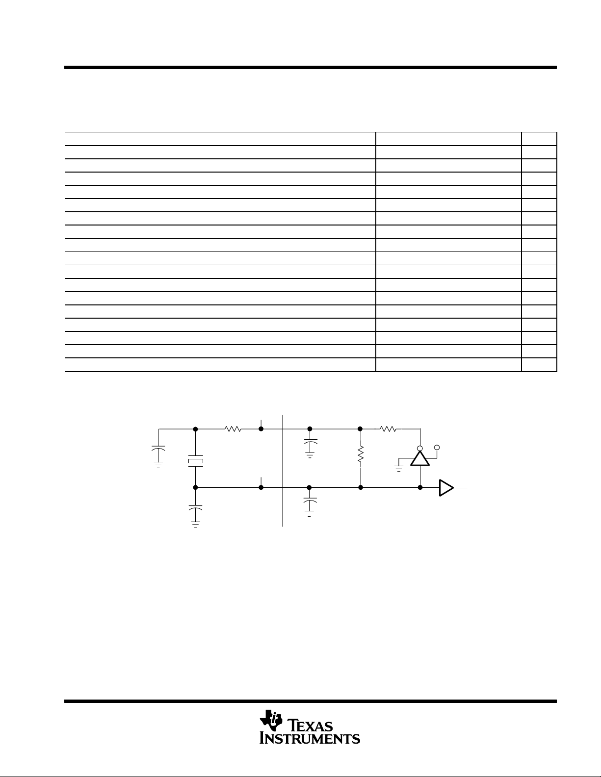
JTAG emulator cable pod logic
Figure 12 shows a portion of the emulator cable pod. The functional features of the pod are as follows:
D Signals TDO and TCK_RET can be parallel-terminated inside the pod if required by the application. By
default, these signals are not terminated.
D Signal TCK is driven with a 74LVT240 device. Because of the high-current drive (32 mA I
OL/IOH
), this signal
can be parallel-terminated. If TCK is tied to TCK_RET, the parallel terminator in the pod can be used.
D Signals TMS and TDI can be generated from the falling edge of TCK_RET, according to the bus slave device
timing rules.
D Signals TMS and TDI are series-terminated to reduce signal reflections.
D A 10.368-MHz test clock source is provided. Another test clock can be used for greater flexibility.
TDO (Pin 7)
GND (Pins 4,6,8,10,12)
EMU0 (Pin 13)
EMU1 (Pin 14)
180 Ω
10.368 MHz
180 Ω
+5 V
270 Ω
JP1
+5 V
270 Ω
74F175
D
74LVT240
A
74AS1034
Q
Q
33 Ω
Y
33 Ω
TMS (Pin 1)
Y
Y
Y
TDI (Pin 3)
TCK (Pin 11)
TRST (Pin 2)
{
20
TCK_RET (Pin 9)
PD(VCC) (Pin 5)
†
The emulator pod uses TCK_RET as its clock source for internal synchronization. TCK is provided as an optional target system
test clock source.
{
JP2
100 Ω
74AS1004
RESIN
TL7705A
Figure 12. JTAG Emulator Cable Pod Interface
POST OFFICE BOX 1443 • HOUSTON, TEXAS 77251-1443
Page 21

SM320VC33, SMJ320VC33
DIGITAL SIGNAL PROCESSOR
SGUS034E - FEBRUARY 2001 - REVISED OCTOBER 2002
device and development support tool nomenclature
To designate the stages in the product development cycle, TI assigns prefixes to the part numbers of all
TMS320 DSP family devices and support tools. Each TMS320 DSP member has one of three prefixes: TMX,
TMP, or TMS. Texas Instruments recommends two of three possible prefix designators for its support tools:
TMDX and TMDS. These prefixes represent evolutionary stages of product development from engineering
prototypes (TMX/TMDX) through fully qualified production devices/tools (TMS/TMDS). This development flow
is defined below.
Device development evolutionary flow:
SMX Experimental device that is not necessarily representative of the final device’s electrical
specifications
TMP Final silicon die that conforms to the device’s electrical specifications but has not completed
quality and reliability verification
SM/SMJ Fully-qualified production device
Support tool development evolutionary flow: TMDX Development support product that has not yet completed Texas Instruments internal qualification
testing.
TMDS Fully qualified development support product TMX and TMP devices and TMDX development support tools are shipped against the following disclaimer: “Developmental product is intended for internal evaluation purposes.” TMS devices and TMDS development support tools have been characterized fully, and the quality and reliability
of the device has been demonstrated fully. TI’s standard warranty applies.
Predictions show that prototype devices (TMX or TMP) have a greater failure rate than the standard production
devices. Texas Instruments recommends that these devices not be used in any production system because their
expected end-use failure rate still is undefined. Only qualified production devices are to be used.
TI device nomenclature also includes a suffix with the device family name. This suffix indicates the package type
(for example, HFG, GNM, or GNL) and temperature range (for example, M). Figure 13 provides a legend for
reading the complete device name for any TMS320 DSP family member.
TMS320 is a trademark of Texas Instruments.
POST OFFICE BOX 1443 • HOUSTON, TEXAS 77251-1443
21
Page 22

SM320VC33, SMJ320VC33
DIGITAL SIGNAL PROCESSOR
SGUS034E - FEBRUARY 2001 - REVISED OCTOBER 2002
device and development support tool nomenclature (continued)
SMJ 320 VC 33 GNM
PREFIX
SMX= experimental device
TMP = prototype device
TMS = qualified device
SMJ = MIL-PRF-38535 (QML)
SMQ = QML Plastic device
SM = Commericial processing
M
150
SPEED
150 = 150 MFLOPS
DEVICE FAMILY
320 = TMS320 Family
TECHNOLOGY
C = CMOS
E = CMOS EPROM
F = CMOS Flash EEPROM
LC = Low-Voltage CMOS (3.3 V)
VC= Low-Voltage CMOS [3 V (2.5 V
or 1.8 V core)]
UC= Ultra Low-Voltage CMOS [1.8 V
(1.5 V core)]
TEMPERATURE RANGE
M = Military
PACKAGE TYPE
HFG = 164-pin ceramic QFP
GNL = 144-pin ceramic BGA, hermetic
GNM= 144-pin ceramic BGA, non-hermetic
DEVICE
3x DSP:
4x DSP:
6x DSP:
†
30
31
32
33
40
44
6201 6201
6701 6211
†
QFP = Quad Flat Package
LQFP = Low-Profile Quad Flat Package
BGA = Ball Grid Array
22
Figure 13. TMS320 DSP Device Nomenclature
POST OFFICE BOX 1443 • HOUSTON, TEXAS 77251-1443
Page 23

SM320VC33, SMJ320VC33
DIGITAL SIGNAL PROCESSOR
SGUS034E - FEBRUARY 2001 - REVISED OCTOBER 2002
absolute maximum ratings over specified temperature range (unless otherwise noted)
Supply voltage range, DV
Supply voltage range, CV
Input voltage range, V
‡
- 0.3 V to 4 V. . . . . . . . . . . . . . . . . . . . . . . . . . . . . . . . . . . . . . . . . . . . . . . . . . . . . .
DD
‡
- 0.3 V to 2.4 V. . . . . . . . . . . . . . . . . . . . . . . . . . . . . . . . . . . . . . . . . . . . . . . . . . . .
DD
§
-1 V to 4.6 V. . . . . . . . . . . . . . . . . . . . . . . . . . . . . . . . . . . . . . . . . . . . . . . . . . . . . . . . . . .
I
†
Output voltage range, VO - 0.3 V to 4.6 V. . . . . . . . . . . . . . . . . . . . . . . . . . . . . . . . . . . . . . . . . . . . . . . . . . . . . . . .
Continuous power dissipation (worst case)¶ 500 mW. . . . . . . . . . . . . . . . . . . . . . . . . . . . . . . . . . . . . . . . . . . . . .
Operating case temperature range, TC -55°C to 125°C. . . . . . . . . . . . . . . . . . . . . . . . . . . . . . . . . . . . . . . . . . . .
Storage temperature range, T
†
Stresses beyond those listed under “absolute maximum ratings” may cause permanent damage to the device. These are stress ratings only, and
functional operation of the device at these or any other conditions beyond those indicated under “recommended operating conditions” is not
implied. Exposure to absolute-maximum-rated conditions for extended periods may affect device reliability.
‡
All voltage values are with respect to VSS.
§
Absolute dc input level should not exceed the DVDD or VSS supply rails by more than 0.3 V. An instantaneous low current pulse of < 2 ns,
< 10 mA, and < 1 V amplitude is permissable.
¶
Actual operating power is much lower. This value was obtained under specially produced worst-case test conditions for the SM/SMJ320VC33,
which are not sustained during normal device operation. These conditions consist of continuous parallel writes of a checkerboard pattern to the
external data and address buses at the maximum possible rate with a capacitive load of 30 pF. See normal (ICC) current specification in the
electrical characteristics table and also read TMS320C3x General-Purpose Applications (literature number SPRU194).
recommended operating conditions
CV
DV
V
V
V
I
I
T
C
‡
§
#
||
kCV
hDV
Supply voltage for the core CPU
DD
Supply voltage for the I/O pinsh 3.14 3.3 3.46 V
DD
Supply ground 0 V
SS
High-level input voltage 0.7 x DV
IH
Low-level input voltage -0.3
IL
High-level output current 4 mA
OH
Low-level output current 4 mA
OL
Operating case temperature -55 125 °C
C
Capacitive load per output pin 30 pF
L
All voltage values are with respect to VSS.
Absolute dc input level should not exceed the DVDD or VSS supply rails by more than 0.3 V. An instantaneous low current pulse of < 2 ns, < 10 mA,
and < 1 V amplitude is permissable.
All inputs and I/O pins are configured as inputs.
All input and I/O pins use a Schmidt hysteresis inputs except SHZ and D0-D31. Hysteresis is approximately 10% of DVDD and is centered at
0.5 x DVDD.
should not exceed DVDD by more than 0.7 V. (Use a Schottky clamp diode between these supplies.)
DD
should not exceed CVDD by more than 2.5 V.
DD
- 55°C to 150°C. . . . . . . . . . . . . . . . . . . . . . . . . . . . . . . . . . . . . . . . . . . . . . . . .
stg
‡#||
MIN NOM MAX UNIT
k
1.71 1.8 1.89 V
DD
§
DVDD + 0.3
0.3 x DV
DD
§
V
V
POST OFFICE BOX 1443 • HOUSTON, TEXAS 77251-1443
23
Page 24

SM320VC33, SMJ320VC33
IDDIDLE2, Supply current, I
DDD
plus I
DDC
DIGITAL SIGNAL PROCESSOR
SGUS034E - FEBRUARY 2001 - REVISED OCTOBER 2002
electrical characteristics over recommended ranges of supply voltage (unless otherwise noted)
PARAMETER TEST CONDITIONS
V
High-level output voltage DVDD = MIN, IOH = MAX 2.4 V
OH
V
Low-level output voltage DVDD = MIN, IOL = MAX 0.4 V
OL
I
High-impedance current TC = 25°C, DVDD = MAX -5 +5 µA
Z
I
Input current TC = 25°C, VI = VSS to DV
I
I
Input current (with internal pullup) Inputs with internal pullups
IPU
I
Input current (with internal pulldown) Inputs with internal pulldowns
IPD
I
Input current (with bus keeper) pullup
BKU
I
Input current (with bus keeper) pulldown
BKD
I
Supply current, pins
DDD
I
Supply current, core CPU
DDC
||
k
||
k
#
#
Bus keeper opposes until conditions match -600 10 µA
TC = 25°C, fx = 75 MHz
DVDD = MAX
TC = 25°C, fx = 75 MHz
CVDD = MAX
PLL enabled, oscillator enabled 2 mA
I
IDLE2, Supply current, I
DD
DDD
plus I
DDC
PLL disabled, oscillator enabled 500
PLL disabled, oscillator disabled, FCLK = 0 50
C
Input capacitance
i
C
Output capacitance 10* pF
o
* Not production tested
†
All voltage values are with respect to VSS.
‡
For test conditions shown as MIN, MAX, or NOM, use the appropriate value specified in the recommended operating conditions table.
§
For VC33, all typical values are at DVDD = 3.3, CVDD = 1.8 V, TC (case temperature) = 25°C.
¶
Pins with internal pullup devices: TDI, TCK, and TMS. Pin with internal pulldown device: TRST.
#
Pins D0-D31 include internal bus keepers that maintain valid logic levels when the bus is not driven (see Figure 9).
||
Actual operating current is less than this maximum value. This value was obtained under specially produced worst-case test conditions, which
All inputs except XIN 10*
XIN 10*
are not sustained during normal device operation. These conditions consist of continuous parallel writes of a checkerboard pattern at the
maximum rate possible. See TMS320C3x General-Purpose Applications (literature number SPRU194).
kf
is the PLL output clock frequency.
x
‡
DD
¶
¶
MIN TYP§MAX UNIT
-5 +5 µA
-600 10 µA
600 -10 µA
600 -10 µA
25 260 mA
60 215 mA
µA
pF
†
Where: I
Tester Pin
Electronics
OL
IO and I
V
LOAD
C
T
PARAMETER MEASUREMENT INFORMATION
I
OL
50 Ω
V
Load
C
T
I
OH
= 4 mA (all outputs) for dc levels test.
are adjusted during ac timing analysis to achieve an ac termination of 50 Ω
OH
=DVDD/2
= 40-pF typical load-circuit capacitance
Figure 14. Test Load Circuit
Output
Under
Test
24
POST OFFICE BOX 1443 • HOUSTON, TEXAS 77251-1443
Page 25

SM320VC33, SMJ320VC33
DIGITAL SIGNAL PROCESSOR
SGUS034E - FEBRUARY 2001 - REVISED OCTOBER 2002
PARAMETER MEASUREMENT INFORMATION
timing parameter symbology
Timing parameter symbols used herein were created in accordance with JEDEC Standard 100. To shorten the
symbols, some of the pin names and other related terminology have been abbreviated as follows, unless
otherwise noted:
Lowercase subscripts and their meanings Letters and symbols and their meanings
a access time H High
c cycle time (period) L Low
d delay time V Valid
dis disable time Z High Impedance
en enable time
f fall time
h hold time
r rise time
su setup time
t transition time
v valid time
w pulse duration (width)
x unknown, changing, or don’t care level
Additional symbols and their meaning
A Address lines (A23- A0) H H1 and H3
ASYNCH
CLKX CLKX0 HOLDA HOLDA
CLKR CLKR0 IACK IACK
CONTROL Control signals INT INT3- INT0
D Data lines (D31- D0) PAGE PAGE0-PAGE3
DR DR RDY RDY
DX DX RW R/W
EXTCLK EXTCLK RW R/W
FS FSX/R RESET RESET
FSX FSX0 S STRB
FSR FSR0 SCK CLKX/R
GPI General-purpose input SHZ SHZ
GPIO
GPO General-purpose output XF XF0, XF1, or XFx
H1 H1 XF0 XF0
H3 H3 XF1 XF1
Asynchronous reset signals (XF0, XF1, CLKX0, DX0,
FSX0, CLKR0, DR0, FSR0, TCLK0, and TCLK1)
General-purpose input/output; peripheral pin (CLKX0,
CLKR0, DX0, DR0, FSX0, FSR0, TCLK0, and TCLK1)
HOLD HOLD
TCLK TCLK0, TCLK1, or TCLKx
XIN XIN
POST OFFICE BOX 1443 • HOUSTON, TEXAS 77251-1443
25
Page 26
SM320VC33, SMJ320VC33
DIGITAL SIGNAL PROCESSOR
SGUS034E - FEBRUARY 2001 - REVISED OCTOBER 2002
phase-locked loop (PLL) circuit timing
phase-locked loop characteristics using EXTCLK or on-chip crystal oscillator
PARAMETER MIN MAX UNIT
F
pllin
F
pllout
I
pll
P
pll
PLL
dc
PLLJ PLL output jitter, F
PLL
LOCK
* Not production tested
†
Duty cycle is defined as 100*t1/(t1+t2)%
Frequency range, PLL input 5* 15* MHz
Frequency range, PLL output 25* 75* MHz
PLL current, CVDD supply 2* mA
PLL power, CVDD supply 5* mW
PLL output duty cycle at H1 45* 55* %
= 25 MHz 400* ps
pllout
PLL lock time in input cycles 1000 cycles
†
To ensure clean internal clock references, the minimal low and high pulse durations must be maintained. At high
frequencies, this may require a fast rise and fall time as well as a tightly controlled duty cycle. At lower
frequencies, these requirements are less restrictive when in x1 and x0.5 modes. The PLL, however, must have
an input duty cycle of between 40% and 60% for proper operation.
26
POST OFFICE BOX 1443 • HOUSTON, TEXAS 77251-1443
Page 27
SGUS034E - FEBRUARY 2001 - REVISED OCTOBER 2002
clock circuit timing
The following table defines the timing parameters for the clock circuit signals.
circuit parameters for on-chip crystal oscillator† (see Figure 15)
PARAMETER MIN TYP MAX UNIT
V
O
F
O
V
bias
R
fbk
R
out
V
xoutac
V
xinac
V
xoutl
V
xouth
V
inl
V
inh
V
xinh
C
xout
C
xin
t
d(XIN-H1)
I
inl
I
inh
* Not production tested
†
This circuit is intended for series resonant fundamental mode operation.
‡
Signal amplitude is dependent on the crystal and load used.
Oscillator internal supply voltage CV
Fundamental mode frequency range 1* 20* MHz
DC bias point (input threshold) 40* 50 60* %V
Feedback resistance 100* 300 500* kΩ
Small signal ac output impedance 250* 500 1000* Ω
The ac output voltage with test crystal
The ac input voltage with test crystal
V
= V
, I
xin
xinh
V
= V
xin
xinl
= 0, FO=0 (logic input) VSS - 0.1* VSS + 0.3* V
xout
, I
= 0, FO=0 (logic input) CVDD - 0.3* CVDD + 0.1* V
xout
‡
‡
When used for logic level input, oscillator enabled -0.3* 0.2 x VO* V
When used for logic level input, oscillator enabled 0.8 x VO* DVDD + 0.3* V
When used for logic level input, oscillator disabled 0.7 x DV
XOUT internal load capacitance 2* 3 5* pF
XIN internal load capacitance 2* 3 5* pF
Delay time, XIN to H1 x1 and x0.5 modes 2 5.5 8 ns
Input current, feedback enabled, Vil = 0 50* µA
Input current, feedback enabled, Vil = V
ih
SM320VC33, SMJ320VC33
DIGITAL SIGNAL PROCESSOR
V
O
O
O
DD
DD
85 %V
85 %V
DVDD + 0.3 V
-50* µA
C
1
C
2
NOTE A: See Table 3 for value of Rd.
XOUT
Rd
C
XOUT
Crystal
XIN
C
XIN
Figure 15. On-Chip Oscillator Circuit
R
OUT
R
fbk
V
O
To internal
clock generator
POST OFFICE BOX 1443 • HOUSTON, TEXAS 77251-1443
27
Page 28

SM320VC33, SMJ320VC33
)
t
w(EXTCLKL)
Pulse duration, EXTCLK low
ns
)
t
w(EXTCLKH)
Pulse duration, EXTCLK high
ns
)
)
)]
t
dc(EXTCLK)
Duty cycle, EXTCLK [t
w(EXTCLKH)
/ t
c(H)]
%
)
t
c(EXTCLK)
Cycle time, EXTCLK
ns
)
F
ext
Frequency range, 1/t
c(EXTCLK)
MHz
Delay time, EXTCLK to H1 and
)
t
c(H)
Cycle time, H1 and H3
ns
DIGITAL SIGNAL PROCESSOR
SGUS034E - FEBRUARY 2001 - REVISED OCTOBER 2002
clock circuit timing (continued)
The following tables define the timing requirements and switching characteristics for EXTCLK.
timing requirements for EXTCLK, all modes (see Figure 16 and Figure 17)
t
r(EXTCLK)
t
f(EXTCLK)
t
w(EXTCLKL
t
w(EXTCLKH
t
dc(EXTCLK
t
c(EXTCLK
F
ext
Rise time, EXTCLK
Fall time, EXTCLK
Pulse duration, EXTCLK low
Pulse duration, EXTCLK high
Duty cycle, EXTCLK [t
Cycle time, EXTCLK
Frequency range, 1/t
* Not production tested
w(EXTCLKH
c(EXTCLK
/ t
c(H
F = F
F < F
F = F
F < F
x5 mode 21*
x1 mode 6*
x0.5 mode 4*
x5 mode 21*
x1 mode 5*
x0.5 mode 4*
x5 PLL mode 40* 60*
x1 and x0.5 modes, F = max 45 55
x1 and x0.5 modes, F = 0 Hz 0* 100*
x5 mode 66.7* 200*
x1 mode 13.3
x0.5 mode 10*
x5 mode 5* 15*
x1 mode 0 75
x0.5 mode 0* 100*
, x0.5 and x1 modes 1*
max
max
, x0.5 and x1 modes 1*
max
max
MIN MAX UNIT
4*
4*
ns
ns
ns
ns
%
ns
MHz
switching characteristics for EXTCLK over recommended operating conditions, all modes
(see Figure 16 and Figure 17)
PARAMETER MIN TYP MAX UNIT
V
mid
t
d(EXTCLK-H)
t
r(H)
t
f(H)
t
d(HL-HH)
t
c(H
* Not production tested
Mid-level, used to measure duty cycle 0.5 x DV
Delay time, EXTCLK to H1 and
H3
x1 mode 2* 4.5 7*
x0.5 mode 2* 4.5 7*
DD
ns
Rise time, H1 and H3 3* ns
Fall time, H1 and H3 3* ns
Delay time, from H1 low to H3 high or from H3 low to H1 high -1.5* 2* ns
x5 PLL mode 1/(5 x fext)
Cycle time, H1 and H3
x1 mode 1/fext
ns
x0.5 mode 2/fext
V
28
POST OFFICE BOX 1443 • HOUSTON, TEXAS 77251-1443
Page 29
clock circuit timing (continued)
SM320VC33, SMJ320VC33
DIGITAL SIGNAL PROCESSOR
SGUS034E - FEBRUARY 2001 - REVISED OCTOBER 2002
EXTCLK
H3
H1
EXTCLK
t
c(EXTCLK)
t
d(EXTCLK-H)
t
c(H)
t
r(EXTCLK)
t
d(EXTCLK-H)
t
r(H)
t
f(EXTCLK)
Figure 16. Divide-By-Two Mode
t
c(EXTCLK)
t
r(EXTCLK)
t
w(EXTCLKH)
t
d(EXTCLK-H)
t
f(EXTCLK)
t
d(EXTCLK-H)
t
w(EXTCLKL)
t
w(EXTCLKL)
t
w(EXTCLKH)
t
f(H)
H3
H1
NOTE A: EXTCLK is held low.
t
c(H)
Figure 17. Divide-By-One Mode
t
d(HL-HH)
POST OFFICE BOX 1443 • HOUSTON, TEXAS 77251-1443
29
Page 30

SM320VC33, SMJ320VC33
DIGITAL SIGNAL PROCESSOR
SGUS034E - FEBRUARY 2001 - REVISED OCTOBER 2002
memory read/write timing
The following tables define memory read/write timing parameters for STRB.
timing requirements for memory read/write† (see Figure 18, Figure 19, and Figure 20)
MIN MAX UNIT
t
su(D-H1L)R
t
h(H1L-D)R
t
su(RDY-H1H)
t
h(H1H-RDY)
t
d(A-RDY)
t
v(A-D)
* Not production tested
†
These timings assume a similar loading of 30 pF on all pins.
‡
P = t
c(H)
switching characteristics over recommended operating conditions for memory read/write†
(see Figure 18, Figure 19, and Figure 20)
t
d(H1L-SL)
t
d(H1L-SH)
t
d(H1H-RWL)W
t
d(H1L-A)
t
d(H1H-RWH)W
t
d(H1H-A)W
t
v(H1L-D)W
t
h(H1H-D)W
* Not production tested
†
These timings assume a similar loading of 30 pF on all pins.
Setup time, Data before H1 low (read) 5* ns
Hold time, Data after H1 low (read) -1* ns
Setup time, RDY before H1 high 5 ns
Hold time, RDY after H1 high -1* ns
Delay time, Address valid to RDY P - 6*
Valid time, Data valid after address PAGEx, or STRB valid
0 wait state, CL = 30 pF 6* ns
1 wait state t
/2 (when duty cycle equals 50%).
PARAMETER MIN MAX UNIT
Delay time, H1 low to STRB low -1* 3 ns
Delay time, H1 low to STRB high -1* 3 ns
Delay time, H1 high to R/W low (write) -1* 3 ns
Delay time, H1 low to address valid -1* 3 ns
Delay time, H1 high to R/W high (write) -1* 3 ns
Delay time, H1 high to address valid on back-to-back write cycles (write) -1* 3* ns
Valid time, Data after H1 low (write) 5 ns
Hold time, Data after H1 high (write) 0* 5 ns
+ 6* ns
c(H)
‡
ns
Output load characteristics for high-speed and low-speed (low-noise) output buffers are shown in Figure 18.
High-speed buffers are used on A0 - A23, PAGE0 - PAGE3, H1, H3, STRB, and R/W. All other outputs use the
low-speed, (low-noise) output buffer.
5
4
3
2
Output Delay (ns)
1
10 20 30 5040
Load Capacitance (pF)
C
Lmax
= 30 pF
Low-Noise Buffer
0.05 ns/pF
High-Speed Buffer
0.04 ns/pF
LOAD
0 pF
15 pF
30 pF
50 pF
HIGH
SPEED
2.0
2.6
3.2
4.0
LOW
NOISE
2.8
3.4
4.4
5.25
Figure 18. Output Load Characteristics, Buffer Only
30
POST OFFICE BOX 1443 • HOUSTON, TEXAS 77251-1443
Page 31
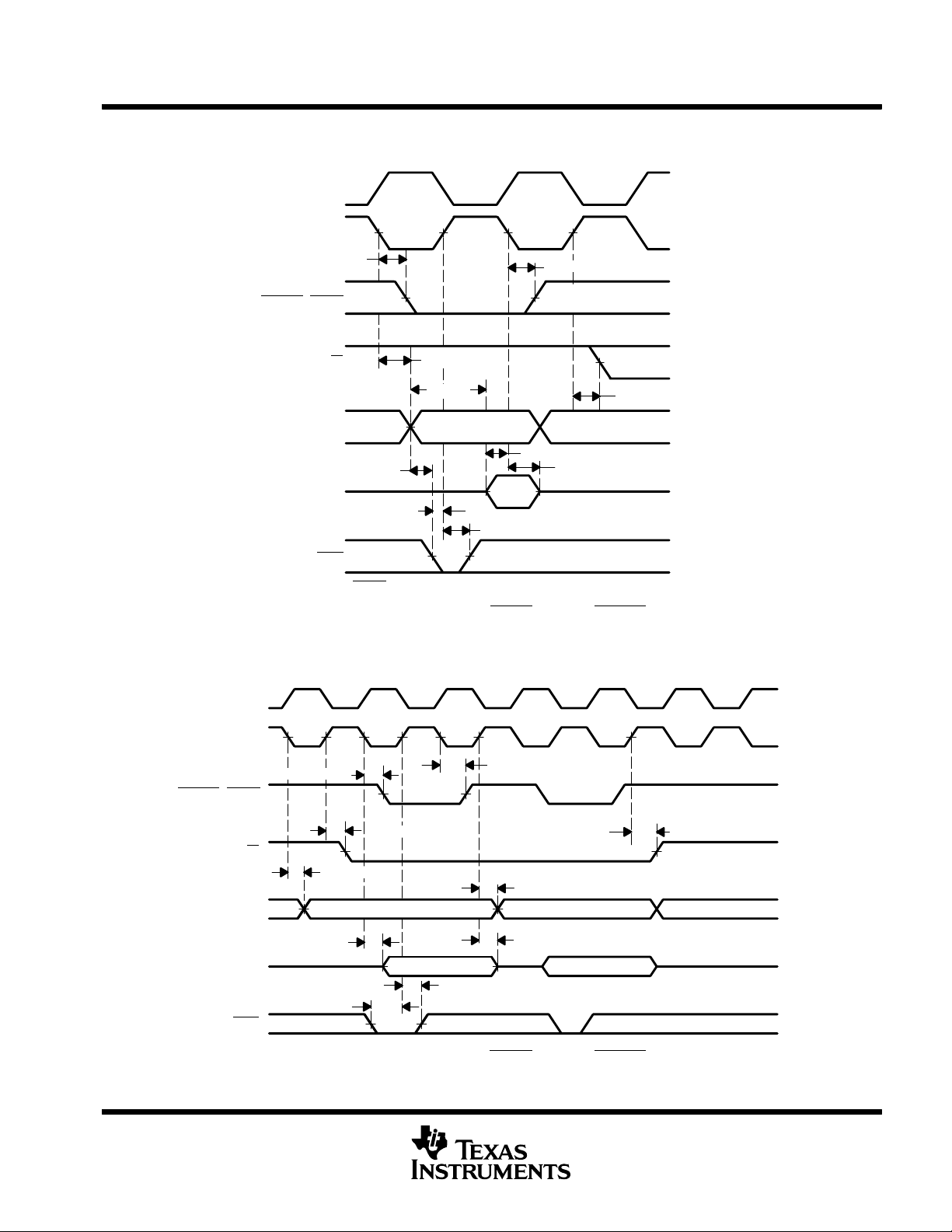
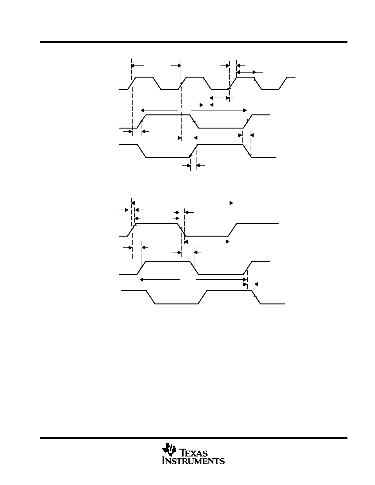
memory read/write timing (continued)
H3
H1
t
d(H1L-SL)
PAGEx, STRB
SM320VC33, SMJ320VC33
DIGITAL SIGNAL PROCESSOR
SGUS034E - FEBRUARY 2001 - REVISED OCTOBER 2002
t
d(H1L-SH)
H3
H1
PAGEx, STRB
R/W
t
d(H1L-A)
t
v(A-D)
t
d(H1H-RWL)W
A[23:0]
t
su(D-H1L)R
t
d(A-RDY)
t
h(H1L-D)R
D[31:0]
t
su(RDY-H1H)
t
h(H1H-RDY)
RDY
NOTE A: STRB remains low during back-to-back read operations.
Figure 19. Timing for Memory (STRB = 0 and PAGEx = 0) Read
t
t
d(H1L-SL)
d(H1L-SH)
t
d(H1H-RWL)W
R/W
t
d(H1L-A)
t
d(H1H-A)W
A[23:0]
t
v(H1L-D)W
t
h(H1H-D)W
D[31:0]
t
h(H1H-RDY)
t
su(RDY-H1H)
RDY
Figure 20. Timing for Memory (STRB = 0 and PAGEx = 0) Write
POST OFFICE BOX 1443 • HOUSTON, TEXAS 77251-1443
t
d(H1H-RWH)W
31
Page 32

SM320VC33, SMJ320VC33
DIGITAL SIGNAL PROCESSOR
SGUS034E - FEBRUARY 2001 - REVISED OCTOBER 2002
XF0 and XF1 timing when executing LDFI or LDII
The following tables define the timing parameters for XF0 and XF1 during execution of LDFI or LDII.
timing requirements for XF0 and XF1 when executing LDFI or LDII (see Fi gure 21)
MIN MAX UNIT
t
su(XF1-H1L)
t
h(H1L-XF1)
* Not production tested
switching characteristics over recommended operating conditions for XF0 and XF1 when executing
LDFI or LDII (see Figure 21)
t
d(H3H-XF0L)
Setup time, XF1 before H1 low 4* ns
Hold time, XF1 after H1 low 0* ns
PARAMETER MIN MAX UNIT
Delay time, H3 high to XF0 low 3 ns
H3
H1
PAGEx, STRB
R/W
A[23:0]
D[31:0]
RDY
XF0
Fetch
LDFI or LDII
t
su(XF1-H1L)
Decode Read Execute
t
d(H3H-XF0L)
32
t
h(H1L-XF1)
XF1
Figure 21. Timing for XF0 and XF1 When Executing LDFI or LDII
POST OFFICE BOX 1443 • HOUSTON, TEXAS 77251-1443
Page 33

SM320VC33, SMJ320VC33
DIGITAL SIGNAL PROCESSOR
SGUS034E - FEBRUARY 2001 - REVISED OCTOBER 2002
XF0 timing when executing STFI and STII
†
The following table defines the timing parameters for the XF0 pin during execution of STFI or STII.
switching characteristics over recommended operating conditions for XF0 when executing STFI
or STII (see Figure 22)
PARAMETER MIN MAX UNIT
t
d(H3H-XF0H)
†
XF0 is always set high at the beginning of the execute phase of the interlock-store instruction. When no pipeline conflicts occur, the address of
the store is also driven at the beginning of the execute phase of the interlock-store instruction. However, if a pipeline conflict prevents the store
from executing, the address of the store will not be driven until the store can execute.
Delay time, H3 high to XF0 high
Fetch
STFI or STII
H3
H1
PAGEx, STRB
R/W
A[23:0]
†
Read ExecuteDecode
3 ns
D[31:0]
RDY
XF0
t
d(H3H-XF0H)
Figure 22. Timing for XF0 When Executing an STFI or STII
POST OFFICE BOX 1443 • HOUSTON, TEXAS 77251-1443
33
Page 34

SM320VC33, SMJ320VC33
DIGITAL SIGNAL PROCESSOR
SGUS034E - FEBRUARY 2001 - REVISED OCTOBER 2002
XF0 and XF1 timing when executing SIGI
The following tables define the timing parameters for the XF0 and XF1 pins during execution of SIGI.
timing requirements for XF0 and XF1 when executing SIGI (see Figure 23)
MIN MAX UNIT
t
su(XF1-H1L)
t
h(H1L-XF1)
* Not production tested
switching characteristics o ver r ecommended o perating c onditions for X F0 a nd X F1 w hen e xecuting
SIGI (see Figure 23)
t
d(H3H-XF0L)
t
d(H3H-XF0H)
Setup time, XF1 before H1 low 4* ns
Hold time, XF1 after H1 low 0* ns
PARAMETER MIN MAX UNIT
Delay time, H3 high to XF0 low 3 ns
Delay time, H3 high to XF0 high 3 ns
H3
H1
XF0
XF1
Fetch
SIGI
t
su(XF1-H1L)
Decode Read Execute
t
h(H1L-XF1)
t
d(H3H-XF0L)
t
d(H3H-XF0H)
Figure 23. Timing for XF0 and XF1 When Executing SIGI
34
POST OFFICE BOX 1443 • HOUSTON, TEXAS 77251-1443
Page 35

SM320VC33, SMJ320VC33
DIGITAL SIGNAL PROCESSOR
SGUS034E - FEBRUARY 2001 - REVISED OCTOBER 2002
loading when XF is configured as an output
The following table defines the timing parameter for loading the XF register when the XFx pin is configured as
an output.
switching characteristics over recommended operating conditions fo r loading the X F registe r when
configured as an output pi n (see Figure 24)
PARAMETER MIN MAX UNIT
t
v(H3H-XF)
Valid time, XFx after H3 high 3 ns
Fetch Load
Instruction
H3
H1
OUTXFx Bit
(see Note A)
XFx
NOTE A: OUTXFx represents either bit 2 or 6 of the IOF register.
Decode Read Execute
Figure 24. Timing for Loading XF Register When Configured as an Output Pin
1 or 0
t
v(H3H-XF)
POST OFFICE BOX 1443 • HOUSTON, TEXAS 77251-1443
35
Page 36

SM320VC33, SMJ320VC33
DIGITAL SIGNAL PROCESSOR
SGUS034E - FEBRUARY 2001 - REVISED OCTOBER 2002
changing XFx from an output to an input
The following table defines the timing parameters for changing the XFx pin from an output pin to an input pin.
timing requirem ents for changing XFx from out put to input mode (see Figure 25)
MIN MAX UNIT
t
su(XF-H1L)
t
h(H1L-XF)
switching characteristics over recommended operating conditions for changin g XFx from outp u t to
input mode (see Figure 25)
t
dis(H3H-XF)
* Not production tested
Setup time, XFx before H1 low 4 ns
Hold time, XFx after H1 low 0 ns
PARAMETER MIN MAX UNIT
Disable time, XFx after H3 high 5* ns
Execute
Load of IOF
H3
H1
I/OxFx Bit
(see Note A)
t
dis(H3H-XF)
XFx
INXFx Bit
(see Note A)
NOTE A: I/OxFx represents either bit 1 or bit 5 of the IOF register, and INXFx represents either bit 3 or bit 7 of the IOF register.
Output
Buffers Go
From Output
to Output
t
su(XF-H1L)
Data
Sampled
Synchronizer
Delay
t
h(H1L-XF)
Value on Pin
Seen in IOF
Data
Seen
Figure 25. Timing for Changing XFx From Output to Input Mode
36
POST OFFICE BOX 1443 • HOUSTON, TEXAS 77251-1443
Page 37

SM320VC33, SMJ320VC33
DIGITAL SIGNAL PROCESSOR
SGUS034E - FEBRUARY 2001 - REVISED OCTOBER 2002
changing XFx from an input to an output
The following table defines the timing parameter for changing the XFx pin from an input pin to an output pin.
switching characteristics over recommended operating conditions for changing XFx from input to
output mode (see Figure 26)
PARAMETER MIN MAX UNIT
t
d(H3H-XF)
Delay time, H3 high to XFx switching from input to output 3 ns
Execution of
Load of IOF
H3
H1
I/OxFx Bit
(see Note A)
XFx
NOTE A: I/OxFx represents either bit 1 or bit 5 of the IOF register.
Figure 26. Timing for Changing XFx From Input to Output Mode
t
d(H3H-XF)
POST OFFICE BOX 1443 • HOUSTON, TEXAS 77251-1443
37
Page 38

SM320VC33, SMJ320VC33
DIGITAL SIGNAL PROCESSOR
SGUS034E - FEBRUARY 2001 - REVISED OCTOBER 2002
reset timing
RESET is an asynchronous input that can be asserted at any time during a clock cycle. If the specified timings
are met, the exact sequence shown in Figure 27 occurs; otherwise, an additional delay of one clock cycle is
possible.
The asynchronous reset signals include XF0/1, CLKX0, DX0, FSX0, CLKR0, DR0, FSR0, and TCLK0/1.
Resetting the device initializes the bus control register to seven software wait states and therefore results in slow
external accesses until these registers are initialized.
HOLD is a synchronous input that can be asserted during reset. It can take nine CPU cycles before HOLDA
is granted.
The following table defines the timing parameters for the RESET signal. The numbers shown in Figure 27
correspond with those in the NO. column of the following table.
timing requirements for RESET (see Figure 27)
MIN MAX UNIT
t
su(RESET-EXTCLKL)
t
su(RESETH-H1L)
* Not production tested
†
P = t
c(EXTCLK)
Setup time, RESET before EXTCLK low 5* P - 7
Setup time, RESET high before H1 low and after ten H1 clock cycles 5 ns
*†
ns
switching characteristics over recommended operating conditions for RESET (see Figure 27)
PARAMETER MIN* MAX* UNIT
t
d(EXTCLKH-H1H)
t
d(EXTCLKH-H1L)
t
d(EXTCLKH-H3L)
t
d(EXTCLKH-H3H)
t
dis(H1H-DZ)
t
dis(H3H-AZ)
t
d(H3H-CONTROLH)
t
d(H1H-RWH)
t
d(H1H-IACKH)
t
dis(RESETL-ASYNCH)
* Not production tested
‡
High impedance for Dbus is limited to nominal bus keeper Z
§
Asynchronous reset signals include XF0/1, CLKX0, DX0, FSX0, CLKR0, DR0, FSR0, and TCLK0/1.
Delay time, EXTCLK high to H1 high 2 7 ns
Delay time, EXTCLK high to H1 low 2 7 ns
Delay time, EXTCLK high to H3 low 2 7 ns
Delay time, EXTCLK high to H3 high 2 7 ns
Disable time, Data (high impedance) from H1 high
Disable time, Address (high impedance) from H3 high 6 ns
Delay time, H3 high to control signals high 3 ns
Delay time, H1 high to R/W high 3 ns
Delay time, H1 high to IACK high 3 ns
Disable time, Asynchronous reset signals disabled (high impedance) from RESET
§
low
= 15 kΩ.
OUT
‡
6 ns
6 ns
38
POST OFFICE BOX 1443 • HOUSTON, TEXAS 77251-1443
Page 39
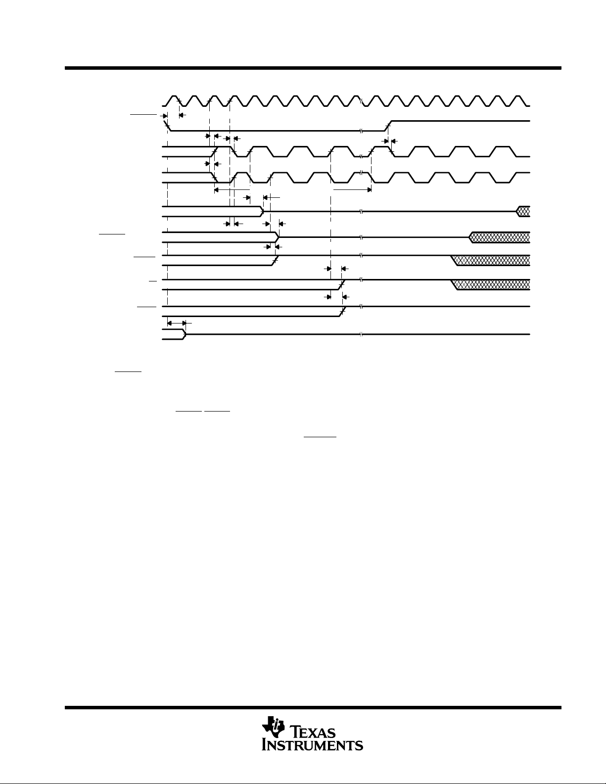
SM320VC33, SMJ320VC33
DIGITAL SIGNAL PROCESSOR
SGUS034E - FEBRUARY 2001 - REVISED OCTOBER 2002
reset timing (continued)
EXTCLK
t
(see Notes A and C)
RESET
t
d(EXTCLKH-H1H)
H1
t
d(EXTCLKH-H3L)
H3
D[31:0]
PAGEx, A[23:0]
STRB
R/W
IACK
Asynchronous
Reset Signals
(see Note B)
NOTES: A. Clock circuit is configured in C31-compatible divide-by-2 mode. If configured for x1 mode, EXTCLK directly drives H3.
B. Asynchronous reset signals include XF0/ 1, CLKX0, DX0, FSX0, CLKR0, DR0, FSR0, and TCLK0/1.
C. RESET is a synchronous input that can be asserted at any point during a clock cycle. If the specified timings are met, the exact
sequence shown occurs; otherwise, an additional delay of one clock cycle is possible.
D. In microprocessor mode, the reset vector is fetched twice, with seven software wait states each time. In microcomputer mode, the
reset vector is fetched twice, with no software wait states.
E. The address and PAGE3-PAGE0 outputs are placed in a high-impedance state during reset requiring a nominal 10-22 kΩ pullup.
If not, undesirable spurious reads can occur when these outputs are not driven.
su(RESET-EXTCLKL)
t
d(EXTCLKH-H3H)
t
dis(RESETL-ASYNCH)
t
d(EXTCLKH-H1L)
Ten H1 Clock Cycles
t
dis(H1H-DZ)
t
dis(H3H-AZ)
t
d(H3H-CONTROLH)
t
d(H1H-RWH)
t
d(H1H-IACKH)
t
su(RESETH-H1L)
Figure 27. RESET Timing
POST OFFICE BOX 1443 • HOUSTON, TEXAS 77251-1443
39
Page 40

SM320VC33, SMJ320VC33
DIGITAL SIGNAL PROCESSOR
SGUS034E - FEBRUARY 2001 - REVISED OCTOBER 2002
interrupt response timing
The following table defines the timing parameters for the INTx signals.
timing requirements for INT3-INT0 response (see Figure 28)
MIN NOM MAX UNIT
t
su(INT-H1L)
t
h(H1L-INT)
t
w(INT)
* Not production tested
†
P = t
c(H)
The interrupt (INTx) pins are synchronized inputs that can be asserted at any time during a clock cycle. The
TMS320C3x interrupts are selectable as level- or edge-sensitive. Interrupts are detected on the falling edge of
H1. Therefore, interrupts must be set up and held to the falling edge of the internal H1 for proper detection. The
CPU and DMA respond to detected interrupts on instruction-fetch boundaries only.
For the processor to recognize only one interrupt when level mode is selected, an interrupt pulse must be set
up and held such that a logic-low condition occurs for:
D A minimum of one H1 falling edge
D No more than two H1 falling edges
D Interrupt sources whose edges cannot be specified to meet the H1 falling edge setup and hold times must
When EDGEMODE=1, the falling edge of the INT0-INT3 pins are detected using synchronous logic (see
Figure 7). The pulse low and high time should be two CPU clocks or greater.
Setup time, INT3- INT0 before H1 low 4* ns
Hold time, INT3- INT0 after H1 low 0 ns
Pulse duration, interrupt to ensure only one interrupt P + 5*†1.5P 2P - 5*
be further restriced in pulse width as defined by t
(parameter 51) in the table above.
w(INT)
†
ns
The TMS320C3x can set the interrupt flag from the same source as quickly as two H1 clock cycles after it has
been cleared.
If the specified timings are met, the exact sequence shown in Figure 28 occurs; otherwise, an additional delay
of one clock cycle is possible.
40
POST OFFICE BOX 1443 • HOUSTON, TEXAS 77251-1443
Page 41

interrupt response timing (continued)
H3
H1
Flag
†
§
t
w(INT)
t
su(INT-H1L)
INT3 - INT0 Pin
(EDGEMODE = 0)
INT3 - INT0 Pin
(EDGEMODE = 1)
INT3 - INT0
t
su(INT-H1L)
t
h(H1L-INT)
‡
t
su(INT-H1L)
SM320VC33, SMJ320VC33
DIGITAL SIGNAL PROCESSOR
SGUS034E - FEBRUARY 2001 - REVISED OCTOBER 2002
Reset or
Interrupt
Vector Read
¶
Fetch First
Instruction of
Service
Routine
ADDR
Vector Address
Data
†
Falling edge of H1 just detects INTx falling edge.
‡
Falling edge of H1 detects second INTx low, however flag clear takes precedence.
§
Nominal width.
¶
Falling edge of H1 misses previous INTx low as INTx rises.
Figure 28. INT3-INT0 Response Timing
First Instruction Address
POST OFFICE BOX 1443 • HOUSTON, TEXAS 77251-1443
41
Page 42

SM320VC33, SMJ320VC33
DIGITAL SIGNAL PROCESSOR
SGUS034E - FEBRUARY 2001 - REVISED OCTOBER 2002
interrupt-acknowledge timing
The IACK output goes active on the first half-cycle (HI rising) of the decode phase of the IACK instruction and
goes inactive at the first half-cycle (HI rising) of the read phase of the IACK instruction.
The following table defines the timing parameters for the IACK signal. The numbers shown in Figure 29
correspond with those in the NO. column of the table below.
NOTE: The IACK instruction can be executed at anytime to signal an event. It is most often used within an
interrupt routine to signal which interrupt has occurred.
switching characteristics over recommended operating conditions for IACK (see Figure 29)
PARAMETER MIN MAX UNIT
t
d(H1H-IACKL)
t
d(H1H-IACKH)
* Not production tested
Delay time, H1 high to IACK low -1* 3 ns
Delay time, H1 high to IACK high -1* 3 ns
H3
H1
IACK
ADDR
Data
Fetch IACK
Instruction
t
d(H1H-IACKL)
Decode IACK
Instruction
IACK Data
Read
Figure 29. Interrupt Acknowledge (IACK) Timing
t
d(H1H-IACKH)
42
POST OFFICE BOX 1443 • HOUSTON, TEXAS 77251-1443
Page 43
serial-port timing parameters
Delay time, CLKX to first DX bit, FSX precedes CLKX
The following tables define the timing parameters for the serial port.
timing requirements (see Figure 30 and Figure 31)
t
c(SCK)
t
w(SCK)
t
r(SCK)
t
f(SCK)
t
su(DR-CLKRL)
t
h(CLKRL-DR)
t
su(FSR-CLKRL)
t
h(SCKL-FS)
t
su(FSX-CLKX)
* Not production tested
†
A cycle time of t
SPRZ176) for further details.
Cycle time, CLKX/R
Pulse duration, CLKX/R high/low
Rise time, CLKX/R 3* ns
Fall time, CLKX/R 3* ns
Setup time, DR before CLKR low
Hold time, DR after CLKR low
Setup time, FSR before CLKR low
Hold time, FSX/R input after CLKX/R low
Setup time, external FSX before CLKX
*2 is possible when the device is operated at lower CPU frequencies. See the TMS320VC33 Silicon Update (literature number
c(H)
SM320VC33, SMJ320VC33
DIGITAL SIGNAL PROCESSOR
SGUS034E - FEBRUARY 2001 - REVISED OCTOBER 2002
MIN MAX UNIT
CLKX/R ext t
CLKX/R int t
CLKX/R ext t
CLKX/R int [t
CLKR ext 4*
CLKR int 5*
CLKR ext 3*
CLKR int 0*
CLKR ext 4*
CLKR int 5*
CLKX/R ext 3*
CLKX/R int 0*
CLKX ext -[t
CLKX int -[t
c(H)
c(H)
c(H)
c(SCK)
c(H)
c(H)
x 2.6*
†
x 4*
+ 5
/2] - 4* [t
- 6] [t
- 10]* t
t
c(H)
c(SCK)
c(SCK)
c(SCK)
x 216*
/2] + 4*
/2] - 6*
/2*
ns
ns
ns
ns
ns
ns
ns
switching characteristics over recommended operating conditions (see Figure 30 and Figure 31)
PARAMETER MIN MAX UNIT
t
d(H1H-SCK)
t
d(CLKX-DX)
t
d(CLKX-FSX)
t
d(CLKX-DX)V
t
d(FSX-DX)V
t
dis(CLKX-DXZ)
* Not production tested
Delay time, H1 high to internal CLKX/R 4* ns
Delay time, CLKX to DX valid
Delay time, CLKX to internal FSX high/low
Delay time, CLKX to first DX bit, FSX precedes CLKX
high
CLKX ext 6
CLKX int 5*
CLKX ext 5
CLKX int 4*
CLKX ext 4
CLKX int 5*
ns
ns
ns
Delay time, FSX to first DX bit, CLKX precedes FSX 6 ns
Disable time, DX high impedance following last data bit from CLKX high 6 ns
POST OFFICE BOX 1443 • HOUSTON, TEXAS 77251-1443
43
Page 44

SM320VC33, SMJ320VC33
DIGITAL SIGNAL PROCESSOR
SGUS034E - FEBRUARY 2001 - REVISED OCTOBER 2002
data-rate timing modes
Unless otherwise indicated, the data-rate timings shown in Figure 30 and Figure 31 are valid for all serial-port
modes, including handshake. For a functional description of serial-port operation, see the TMS320C3x User’s
Guide (literature number SPRU031).
The serial-port timing parameters are defined in the preceding “serial-port timing parameters” tables. The
numbers shown in Figure 30 and Figure 31 correspond with those in the NO. column of each table.
t
c(SCK)
t
w(SCK)
t
d(CLKX- DX)
t
h(CLKRL- DR)
t
su(DR- CLKRL)
Bit n-1 Bit n-2
t
w(SCK)
Bit 0
t
f(SCK)
t
dis(CLKX- DXZ)
H1
CLKX/R
DX
DR
FSR
t
d(CLKX- FSX)
FSX(INT)
FSX(EXT)
t
d(H1H-SCK)
t
d(H1H-SCK)
t
d(CLKX- DX)V
t
su(FSR- CLKRL)
t
h(SCKL- FS)
Bit n-1 Bit n-2
t
d(CLKX- FSX)
t
r(SCK)
t
su(FSX- CLKX)
t
h(SCKL- FS)
NOTES: A. Timing diagrams show operations with CLKXP = CLKRP = FSXP = FSRP = 0.
B. Timing diagrams depend on the length of the serial-port word, where n = 8, 16, 24, or 32 bits, respectively.
Figure 30. Fixed Data-Rate Mode Timing
CLKX/R
FSX(INT)
t
su(FSX- CLKX)
FSX(EXT)
t
d(CLKX-DX)V
DX
FSR
DR
t
su(DR- CLKRL)
NOTES: A. Timing diagrams show operation with CLKXP = CLKRP = FSXP = FSRP = 0.
B. Timing diagrams depend on the length of the serial-port word, where n = 8, 16, 24, or 32 bits, respectively.
C. The timings that are not specified expressly for the variable data-rate mode are the same as those that are specified for the fixed
data-rate mode.
t
d(CLKX- FSX)
t
d(FSX- DX)V
Bit n-1
t
h(SCKL-FS)
t
su(FSR-CLKRL)
t
h(CLKRL-DR)
t
d(CLKX- DX)
Bit n-2 Bit n-3Bit n-1
Bit n-2 Bit n-3
Figure 31. Variable Data-Rate Mode Timing
t
dis(CLKX-DXZ)
Bit 0
44
POST OFFICE BOX 1443 • HOUSTON, TEXAS 77251-1443
Page 45

SM320VC33, SMJ320VC33
DIGITAL SIGNAL PROCESSOR
SGUS034E - FEBRUARY 2001 - REVISED OCTOBER 2002
HOLD timing
HOLD is a synchronous input that can be asserted at any time during a clock cycle. If the specified timings are
met, the exact sequence shown in Figure 32 and Figure 33 occurs; otherwise, an additional delay of one clock
cycle is possible.
The table, “timing parameters for HOLD/HOLDA”, defines the timing parameters for the HOLD and HOLDA
signals. The numbers shown in Figure 32 and Figure 33 correspond with those in the NO. column of the table.
The NOHOLD bit of the primary-bus control register overrides the HOLD signal. When this bit is set, the device
comes out of hold and prevents future hold cycles.
Asserting HOLD prevents the processor from accessing the primary bus. Program execution continues until a
read from or a write to the primary bus is requested. In certain circumstances, the first write is pending, thus
allowing the processor to continue (internally) until a second external write is encountered.
Figure 32, Figure 33, and the accompaning timings are for a zero wait-state bus configuration. Since HOLD is
internally captured by the CPU on the H1 falling edge one cycle before the present cycle is terminated, the
minimum HOLD width for any bus configuration is, therefore, WTCNT+3. Also, HOLD should not be deasserted
before HOLDA has been active for at least one cycle.
timing requirements for HOLD/HOLDA (see Figure 32 and Figure 33)
MIN MAX UNIT
t
su(HOLD-H1L)
t
w(HOLD)
*Not production tested.
Setup time, HOLD before H1 low 3 ns
Pulse duration, HOLD low 3t
* ns
c(H)
switching characteristics over recommended operating conditions for HOLD/HOLDA
(see Figure 32 and Figure 33)
PARAMETER MIN MAX UNIT
t
v(H1L-HOLDA)
t
w(HOLDA)
t
d(H1L-SH)H
t
dis(H1L-S)
t
en(H1L-S)
t
dis(H1L-RW)
t
en(H1L-RW)
t
dis(H1L-A)
t
en(H1L-A)
t
dis(H1H-D)
* Not production tested
Valid time, HOLDA after H1 low -1* 3* ns
Pulse duration, HOLDA low 2t
Delay time, H1 low to STRB high for a HOLD -1 3 ns
Disable time, STRB to the high-impedance state from H1 low 4 ns
Enable time, STRB enabled (active) from H1 low 4 ns
Disable time, R/W to the high-impedance state from H1 low 5* ns
Enable time, R/W enabled (active) from H1 low 4 ns
Disable time, Address to the high-impedance state from H1 low 4* ns
Enable time, Address enabled (valid) from H1 low 5 ns
Disable time, Data to the high-impedance state from H1 high 4* ns
- 4* ns
c(H)
POST OFFICE BOX 1443 • HOUSTON, TEXAS 77251-1443
45
Page 46

SM320VC33, SMJ320VC33
DIGITAL SIGNAL PROCESSOR
SGUS034E - FEBRUARY 2001 - REVISED OCTOBER 2002
HOLD timing (continued)
H3
H1
t
su(HOLD- H1L)
HOLD
t
v(H1L-HOLDA)
HOLDA
STRB, PAGEx
R/W
A[23:0]
D[31:0] Write Data
NOTE A: HOLDA goes low in response to HOLD going low and continues to remain low until one H1 cycle
t
d(H1L-SH)H
after HOLD goes back high.
t
w(HOLD)
t
dis(H1L-RW)
t
dis(H1L-A)
t
dis(H1H-D)
t
dis(H1L-S)
t
t
w(HOLDA)
su(HOLD- H1L)
t
v(H1L- HOLDA)
t
en(H1L-S)
t
en(H1L-RW)
t
en(H1L-A)
Figure 32. Timing for HOLD/HOLDA (After Write)
H3
H1
t
su(HOLD- H1L)
t
w(HOLDA)
HOLD
HOLDA
t
su(HOLD- H1L)
t
d(H1L-SH)H
t
w(HOLD)
t
v(H1L- HOLDA)
t
dis(H1L-S)
STRB, PAGEx
t
dis(H1L-RW)
R/W
t
dis(H1L-A)
A[23:0]
D[31:0] Read Data
NOTE A: HOLDA goes low in response to HOLD going low and continues to remain low until one H1 cycle
after HOLD goes back high.
Figure 33. Timing for HOLD/HOLDA (After Read)
t
v(H1L- HOLDA)
t
en(H1L-S)
t
en(H1L-RW)
t
en(H1L-A)
46
POST OFFICE BOX 1443 • HOUSTON, TEXAS 77251-1443
Page 47

SM320VC33, SMJ320VC33
DIGITAL SIGNAL PROCESSOR
SGUS034E - FEBRUARY 2001 - REVISED OCTOBER 2002
general-purpose I/O timing
Peripheral pins include CLKX0, CLKR0, DX0, DR0, FSX0, FSR0, and TCLK0/1. The contents of the internal
control registers associated with each peripheral define the modes for these pins.
peripheral pin I/O timing
The following table shows the timing parameters for changing the peripheral pin from a general-purpose output
pin to a general-purpose input pin and vice versa.
timing requirements for peripheral pin general-purpose I/O (see Note 1, Figure 34, and Figure 35)
MIN MAX UNIT
t
su(GPIO-H1L)
t
h(H1L-GPIO)
* Not production tested
NOTE 1: Peripheral pins include CLKX0, CLKR0, DX0, DR0, FSX0, FSR0, and TCLK0/1. The modes of these pins are defined by the contents
switching characteristics over recommended operating conditions for peripheral pin
general-purpose I/O (see Note 1, Figure 34, and Figure 35)
t
d(H1H-GPIO)
t
dis(H1H)
NOTE 1: Peripheral pins include CLKX0, CLKR0, DX0, DR0, FSX0, FSR0, and TCLK0/1. The modes of these pins are defined by the contents
Setup time, general-purpose input before H1 low 3* ns
Hold time, general-purpose input after H1 low 0* ns
of internal-control registers associated with each peripheral.
PARAMETER MIN MAX UNIT
Delay time, H1 high to general-purpose output 4 ns
Disable time, general-purpose output from H1 high 5 ns
of internal-control registers associated with each peripheral.
Execution
of Store of
Peripheral-
Control
Register
H3
H1
Control Bit
Peripheral Pin
(see Note A)
NOTE A: Peripheral pins include CLKX0, CLKR0, DX0, DR0, FSX0, FSR0, and TCLK0/1.
I/O
Data Bit
Output
t
dis(H1H)
Buffers Go
t
su(GPIO-H1L)
Data
Sampled
From
Output to
Input
Synchronizer Delay
t
h(H1L-GPIO)
Value on Pin
Seen in
Peripheral-
Control
Register
Data
Seen
Figure 34. Change of Peripheral Pin From General-Purpose Output to Input Mode Timing
POST OFFICE BOX 1443 • HOUSTON, TEXAS 77251-1443
47
Page 48

SM320VC33, SMJ320VC33
DIGITAL SIGNAL PROCESSOR
SGUS034E - FEBRUARY 2001 - REVISED OCTOBER 2002
peripheral pin I/O timing (continued)
Execution of Store
of Peripheral-
Control Register
H3
H1
I/O
Control
Bit
Peripheral Pin
(see Note A)
t
d(H1H-GPIO)
t
d(H1H-GPIO)
NOTE A: Peripheral pins include CLKX0, CLKR0, DX0, DR0, FSX0, FSR0, and TCLK0/1.
Figure 35. Change of Peripheral Pin From General-Purpose Input to Output Mode Timing
48
POST OFFICE BOX 1443 • HOUSTON, TEXAS 77251-1443
Page 49

SM320VC33, SMJ320VC33
‡
DIGITAL SIGNAL PROCESSOR
SGUS034E - FEBRUARY 2001 - REVISED OCTOBER 2002
timer pin timing
Valid logic-level periods and polarity are specified by the contents of the internal control registers. The following
tables define the timing parameters for the timer pin.
timing requirements for timer pin (see Figure 36 and Figure 37)
MIN MAX UNIT
t
su(TCLK-H1L)
t
h(H1L-TCLK)
* Not production tested
†
These requirements are applicable for a synchronous input clock.
switching characteristics over recommended operating conditions for timer pin (see Figure 36 and
Figure 37)
†
Setup time, TCLK external before H1 low 3* ns
†
Hold time, TCLK external after H1 low 0 ns
PARAMETER
t
d(H1H-TCLK)
‡
t
c(TCLK)
t
w(TCLK)
* Not production tested
‡
These parameters are applicable for an asynchronous input clock.
Delay time, H1 high to TCLK internal valid 3 ns
Cycle time, TCLK
Pulse duration, TCLK
H3
H1
t
h(H1L-TCLK)
t
su(TCLK-H1L)
TCLK as input
Figure 36. Timer Pin Timing, Input
H3
TCLK ext t
TCLK int t
TCLK ext t
TCLK int [t
t
t
c(TCLK)
su(TCLK-H1L)
MIN MAX UNIT
x 2.6*
c(H)
x 2* t
c(H)
+ 5*
c(H)
/2] - 4* [t
c(TCLK)
t
h(H1L-TCLK)
t
w(TCLK)
c(H)
c(TCLK)
x 232*
/2] + 4*
ns
ns
H1
t
d(H1H-TCLK)
t
d(H1H-TCLK)
TCLK as output
Figure 37. Timer Pin Timing, Output
POST OFFICE BOX 1443 • HOUSTON, TEXAS 77251-1443
49
Page 50

SM320VC33, SMJ320VC33
DIGITAL SIGNAL PROCESSOR
SGUS034E - FEBRUARY 2001 - REVISED OCTOBER 2002
SHZ pin timing
The following table defines the timing parameter for the SHZ pin.
switching characteristics over recommended operating conditions for SHZ (see Figure 38)
PARAMETER MIN MAX UNIT
t
dis(SHZ)
* Not production tested
Disable time, SHZ low to all outputs, I/O pins disabled (high impedance) 0* 8* ns
SHZ
t
All I/O Pins
dis(SHZ)
NOTE A: Enabling SHZ destroys SM/SMJ320VC33 register and memory contents.
Assert SHZ = 1 and reset the SM/SMJ320VC33 to restore it to a known
condition.
Figure 38. Timing for SHZ
test access port timing
The following table defines the timing parameter for the test access port.
timing for test access port (see Figure 39)
t
su(TMS-TCKH)
t
h(TCKH-TMS)
t
d(TCKL-TDOV)
t
r (TCK)
t
f (TCK)
* Not production tested
Setup time, TMS/TDI to TCK high 5* ns
Hold time, TMS/TDI from TCK high 5* ns
Delay time, TCK low to TDO valid 0* 10* ns
Rise time, TCK 3* ns
Fall time, TCK 3* ns
TCK
t
r(TCK)
TMS/TDI
t
f(TCK)
t
su(TMS-TCKH)
MIN MAX UNIT
50
TDO
t
d(TCHL-TDOV)
Figure 39. IEEE-1149.1 Test Access Port Timings
POST OFFICE BOX 1443 • HOUSTON, TEXAS 77251-1443
t
h(TCHK-TMS)
Page 51

SM320VC33, SMJ320VC33
DIGITAL SIGNAL PROCESSOR
SGUS034E - FEBRUARY 2001 - REVISED OCTOBER 2002
MECHANICAL DATA
GNM (S-CBGA-N144) CERAMIC BALL GRID ARRAY
12,15
11,85
SQ
N
M
L
K
J
H
G
F
E
D
C
B
A
9,60 TYP
0,80
0,80
0,56
0,34
0,55
0,45
NOTES: A. All linear dimensions are in millimeters.
B. This drawing is subject to change without notice.
∅ 0,10
5132 4 6 7 8 9 10111213
2,40 MAX
Seating Plane
M
0,50
0,35
0,12
4201017/B 05/01
POST OFFICE BOX 1443 • HOUSTON, TEXAS 77251-1443
51
Page 52

SM320VC33, SMJ320VC33
DIGITAL SIGNAL PROCESSOR
SGUS034E - FEBRUARY 2001 - REVISED OCTOBER 2002
MECHANICAL DATA
HFG (S-CQFP-F164) CERAMIC QUAD FLATPACK WITH NCTB
”A”
42
82
0.061 (1,55)
0.059 (1,50)
1.140 (28,96)
1.120 (28,45)
1.000 (25,40)
41
83
1.150 (29,21)
BSC 8 Places
DIA 4 Places
BSC
SQ
1
123
0.325 (8,26)
0.275 (6,99)
164
1.520 (38,61)
1.480 (37,59)
124
Tie Bar Width
2.505 (63,63)
2.485 (63,12)
”C”
”B”
0.105 (2,67) MAX
0.010 (0,25)
164 X
0.006 (0,15)
BRAZE
0,025 (0,64)
DETAIL ”A”
NOTES: C. All linear dimensions are in inches (millimeters).
D. This drawing is subject to change without notice.
E. Ceramic quad flatpack with flat leads brazed to non-conductive tie bar carrier
F. This package is hermetically sealed with a metal lid.
G. The leads are gold-plated and can be solder-dipped.
H. Leads not shown for clarity purposes
I. Falls within JEDEC MO-113AA (REV D)
0.020 (0,51) MAX
DETAIL ”B”
0.040 (1,02)
0.030 (0,76)
0.009 (0,23)
0.004 (0,10)
DETAIL ”C”
0.018 (0,46) MAX
0.014 (0,36)
0.002 (0,05)
0.130 (3,30) MAX
4040231-9/J 01/99
52
POST OFFICE BOX 1443 • HOUSTON, TEXAS 77251-1443
Page 53

PACKAGE OPTION ADDENDUM
www.ti.com
25-Feb-2005
PACKAGING INFORMATION
Orderable Device Status
(1)
Package
Type
Package
Drawing
Pins Package
Qty
Eco Plan
5962-0053901QYA ACTIVE CFP HFG 164 1 None Call TI Level-NC-NC-NC
5962-0053901QYC ACTIVE CFP HFG 164 1 None Call TI Level-NC-NC-NC
5962-0053902QYA ACTIVE CFP HFG 164 1 None Call TI Level-NC-NC-NC
5962-0053902QYC ACTIVE CFP HFG 164 4 None Call TI Level-NC-NC-NC
SM320VC33GNMM150 ACTIVE CBGA GNM 144 1 None Call TI Level-1-235C-UNLIM
SMJ320VC33HFGM150 ACTIVE CFP HFG 164 1 None Call TI Level-NC-NC-NC
(1)
The marketing status values are defined as follows:
ACTIVE: Product device recommended for new designs.
LIFEBUY: TI has announced that the device will be discontinued, and a lifetime-buy period is in effect.
NRND: Not recommended for new designs. Device is in production to support existing customers, but TI does not recommend using this part in
a new design.
PREVIEW: Device has been announced but is not in production. Samples may or may not be available.
OBSOLETE: TI has discontinued the production of the device.
(2)
Eco Plan - May not be currently available - please check http://www.ti.com/productcontent for the latest availability information and additional
product content details.
None: Not yet available Lead (Pb-Free).
Pb-Free (RoHS): TI's terms "Lead-Free" or "Pb-Free" mean semiconductor products that are compatible with the current RoHS requirements
for all 6 substances, including the requirement that lead not exceed 0.1% by weight in homogeneous materials. Where designed to be soldered
at high temperatures, TI Pb-Free products are suitable for use in specified lead-free processes.
Green (RoHS & no Sb/Br): TI defines "Green" to mean "Pb-Free" and in addition, uses package materials that do not contain halogens,
including bromine (Br) or antimony (Sb) above 0.1% of total product weight.
(2)
Lead/Ball Finish MSL Peak Temp
(3)
(3)
MSL, Peak Temp. -- The Moisture Sensitivity Level rating according to the JEDECindustry standard classifications, and peak solder
temperature.
Important Information and Disclaimer:The information provided on this page represents TI's knowledge and belief as of the date that it is
provided. TI bases its knowledge and belief on information provided by third parties, and makes no representation or warranty as to the
accuracy of such information. Efforts are underway to better integrate information from third parties. TI has taken and continues to take
reasonable steps to provide representative and accurate information but may not have conducted destructive testing or chemical analysis on
incoming materials and chemicals. TI and TI suppliers consider certain information to be proprietary, and thus CAS numbers and other limited
information may not be available for release.
In no event shall TI's liability arising out of such information exceed the total purchase price of the TI part(s) at issue in this document sold by TI
to Customer on an annual basis.
Addendum-Page 1
Page 54

IMPORTANT NOTICE
Texas Instruments Incorporated and its subsidiaries (TI) reserve the right to make corrections, modifications,
enhancements, improvements, and other changes to its products and services at any time and to discontinue
any product or service without notice. Customers should obtain the latest relevant information before placing
orders and should verify that such information is current and complete. All products are sold subject to TI’s terms
and conditions of sale supplied at the time of order acknowledgment.
TI warrants performance of its hardware products to the specifications applicable at the time of sale in
accordance with TI’s standard warranty. Testing and other quality control techniques are used to the extent TI
deems necessary to support this warranty . Except where mandated by government requirements, testing of all
parameters of each product is not necessarily performed.
TI assumes no liability for applications assistance or customer product design. Customers are responsible for
their products and applications using TI components. To minimize the risks associated with customer products
and applications, customers should provide adequate design and operating safeguards.
TI does not warrant or represent that any license, either express or implied, is granted under any TI patent right,
copyright, mask work right, or other TI intellectual property right relating to any combination, machine, or process
in which TI products or services are used. Information published by TI regarding third-party products or services
does not constitute a license from TI to use such products or services or a warranty or endorsement thereof.
Use of such information may require a license from a third party under the patents or other intellectual property
of the third party, or a license from TI under the patents or other intellectual property of TI.
Reproduction of information in TI data books or data sheets is permissible only if reproduction is without
alteration and is accompanied by all associated warranties, conditions, limitations, and notices. Reproduction
of this information with alteration is an unfair and deceptive business practice. TI is not responsible or liable for
such altered documentation.
Resale of TI products or services with statements different from or beyond the parameters stated by TI for that
product or service voids all express and any implied warranties for the associated TI product or service and
is an unfair and deceptive business practice. TI is not responsible or liable for any such statements.
Following are URLs where you can obtain information on other Texas Instruments products and application
solutions:
Products Applications
Amplifiers amplifier.ti.com Audio www.ti.com/audio
Data Converters dataconverter.ti.com Automotive www.ti.com/automotive
DSP dsp.ti.com Broadband www.ti.com/broadband
Interface interface.ti.com Digital Control www.ti.com/digitalcontrol
Logic logic.ti.com Military www.ti.com/military
Power Mgmt power.ti.com Optical Networking www.ti.com/opticalnetwork
Microcontrollers microcontroller.ti.com Security www.ti.com/security
Telephony www.ti.com/telephony
Video & Imaging www.ti.com/video
Wireless www.ti.com/wireless
Mailing Address: Texas Instruments
Post Office Box 655303 Dallas, Texas 75265
Copyright 2005, Texas Instruments Incorporated
 Loading...