SMJ320MCM42C, SMJ320MCM42D
DUAL SMJ320C40 MULTICHIP MODULE
SGKS001B – JULY 1997 – REVISED FEBRUARY 2000
1
POST OFFICE BOX 1443 • HOUSTON, TEXAS 77251–1443
D Performance:
– 80 Million Floating-Point Operations Per
Second (MFLOPS) With 496-MBps-Burst
I/O Rate for 40-MHz Modules
– Zero-Wait-State Local Memory for Each
Processor
D Organization:
– 128K-Word × 32-Bit Static
Random-Access Memory (SRAM)
(SMJ320MCM42D)
– 256K-Word × 32-Bit SRAM
(SMJ320MCM42C)
D Compliant With MIL-PRF-38535 QML
D Dual ’C40 Performance With Local Memory
Requiring Only 8.7 Square Inches of Board
Space
D Enhanced Performance Offered By
Multichip-Module Solution
– SMJ320MCM42C
– 67% Reduction in Number of
Interconnects
– 54% Reduction (Minimum) in Board
Area
– Estimated 38% Reduction in Power
Dissipation Due to Reduced Parasitic
Capacitance and Interconnect Lengths
– SMJ320MCM42D
– 56% Reduction in Number of
Interconnects
– 30% Reduction (Minimum) in Board
Area
– Estimated 20% Reduction in Power
Dissipation Due to Reduced Parasitic
Capacitance and Interconnect Lengths
D Four Memory Ports for High Data
Bandwidth
– Two Full 2G-Word External Buses
D Two Internal Buses Mapped to Memory
– 128K-Word × 32-Bit SRAM for Each ’C40
Local Bus (SMJ320MCM42D)
– 256K-Word × 32-Bit SRAM for Each ’C40
Local Bus (SMJ320MCM42C)
D Ten External Communication Ports for
Direct Processor-to-Processor
Communication
D IEEE-1149.1
†
(JTAG) Boundary-Scan
Compatible
D 408-Lead Ceramic Quad Flatpack Package
(HFN Suffix)
D Operating Free-Air Temperature Ranges:
–55°C to 125°C . . . (Military)
0°C to 70°C . . . (Commercial)
D Communication-Port Connection Provided
Between ’C40s for Interprocessor
Communication
Please be aware that an important notice concerning availability, standard warranty, and use in critical applications of
Texas Instruments semiconductor products and disclaimers thereto appears at the end of this data sheet.
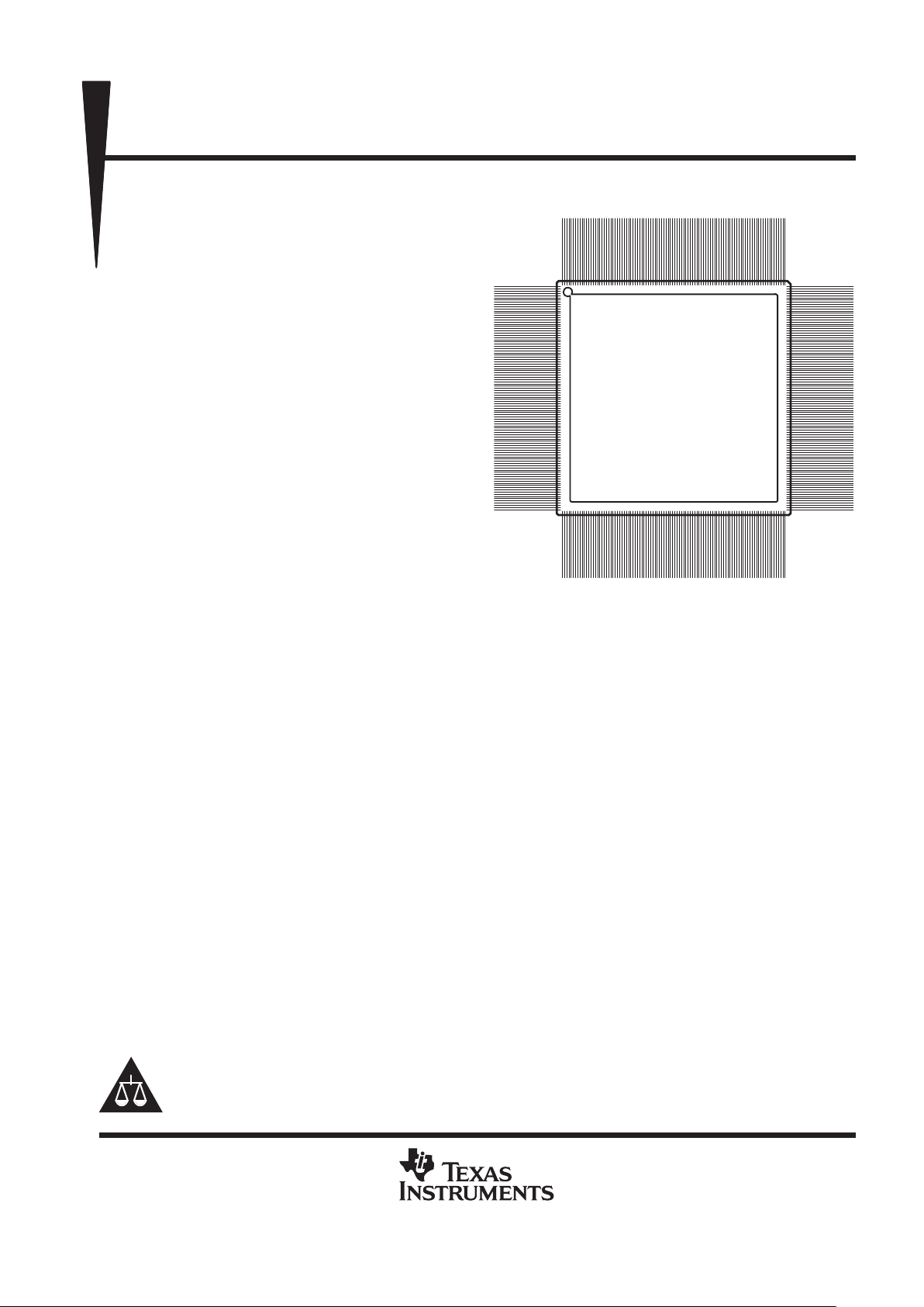
‡
Terminal assignment information is provided by the terminal
assignments table. Package is shown for pinout reference only.
HFN PACKAGE
‡
(TOP VIEW)
306
1
102 205
408 307
103 204
PRODUCTION DATA information is current as of publication date.
Products conform to specifications per the terms of Texas Instruments
standard warranty. Production processing does not necessarily include
testing of all parameters.
Copyright 2000, Texas Instruments Incorporated
†
IEEE Standard 1149.1–1990 Standard Test-Access Port and Boundary-Scan Architecture
On products compliant to MIL-STD-PRF-38535, all parameters
are tested unless otherwise noted. On all other products,
production processing does not necessarily include testing of all
parameters.

SMJ320MCM42C, SMJ320MCM42D
DUAL SMJ320C40 MULTICHIP MODULE
SGKS001B – JULY 1997 – REVISED FEBRUARY 2000
2
POST OFFICE BOX 1443 • HOUSTON, TEXAS 77251–1443
description
The ’42 dual ’C40 multichip module (MCM) contains two SMJ320C40 digital signal processors (DSPs) with
128K words × 32 bits (’42D) or 256K words × 32 bits (’42C) of zero-wait-state SRAMs mapped to each local
bus. Global address and data buses with two sets of control signals are routed externally for each processor,
allowing external memory to be accessed. The external global bus provides a continuous address reach of
2G words.
The dual ’C40 configuration allows standard microprocessor initialization using the bootstrap loader. Both
reset-vector-control terminals are brought out to external terminals for each processor. A single CLKIN line and
a RESET line feed both processors in parallel, minimizing clock skew and allowing easy synchronization for
interlocked operations.
Communication port 0 of CPU #1 connects to communication port 3 of CPU #2 for direct processor-to-processor
communication.
The IEEE-1 149.1 (JT AG) test ports of the ’C40s are connected serially to allow scan operations and emulation
of the module as a whole. T estability of the ’42 adds value and reduces development and support costs. Texas
Instruments (TI) offers a wide variety of ANSI/IEEE-1149.1 products and support.
The ’42 dual ’C40 MCM is packaged in a 408-pin ceramic quad flat pack. The ’42 dual ’C40 MCM is available
in both a commercial temperature range (0°C to 70°C) and a military temperature range (–55°C to 125°C)
option.
TI is a trademark of Texas Instruments Incorporated.

SMJ320MCM42C, SMJ320MCM42D
DUAL SMJ320C40 MULTICHIP MODULE
SGKS001B – JULY 1997 – REVISED FEBRUARY 2000
3
POST OFFICE BOX 1443 • HOUSTON, TEXAS 77251–1443
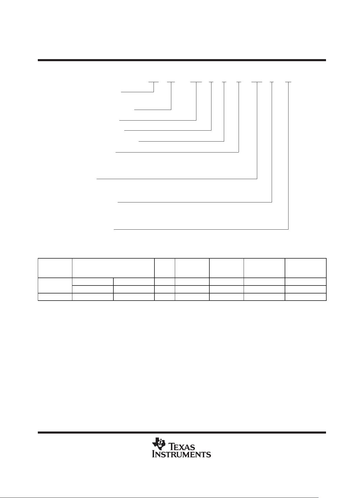
device symbol nomenclature
Example: SMJ 320 MCM 4 2 C HFN M 40
Process-Level Prefix
(See Table 1)
320 DSP Family Designator
Multichip Module
Processor Family
Number of CPUs per Module
Module Revision
Package
HFN = 408-Lead Ceramic Quad Flatpack
Temperature Range
L=0°C to 70°C
M= –55°C to 125°C
Speed Designator
40 = 40 MHz
’42C = 256K-word × 32-bit SRAM
’42D = 128K-word
× 32-bit SRAM
Table 1. MCM Processing Matrix
PROCESS
LEVEL
TEMPERATURE RANGE DIE
100%
PROCESSED
SPEED
TEST
TEST
TEMPERATURE
RANGE
QUALIFICATION
TESTING
L version 0°C to 70°C Probed No No 25°C to 70°C Package
SM
M version –55°C to 125°C Probed No Yes –55°C to 125°C Package
SMJ
†
M version –55°C to 125°C KGD
‡
Yes Yes –55°C to 125°C MIL-H-38534
†
SMJ-level product is full MIL-PRF-38535 QML compliant.
‡
KGD stands for the known-good-die strategy as defined in the reference documentation section.

SMJ320MCM42C, SMJ320MCM42D
DUAL SMJ320C40 MULTICHIP MODULE
SGKS001B – JULY 1997 – REVISED FEBRUARY 2000
4
POST OFFICE BOX 1443 • HOUSTON, TEXAS 77251–1443
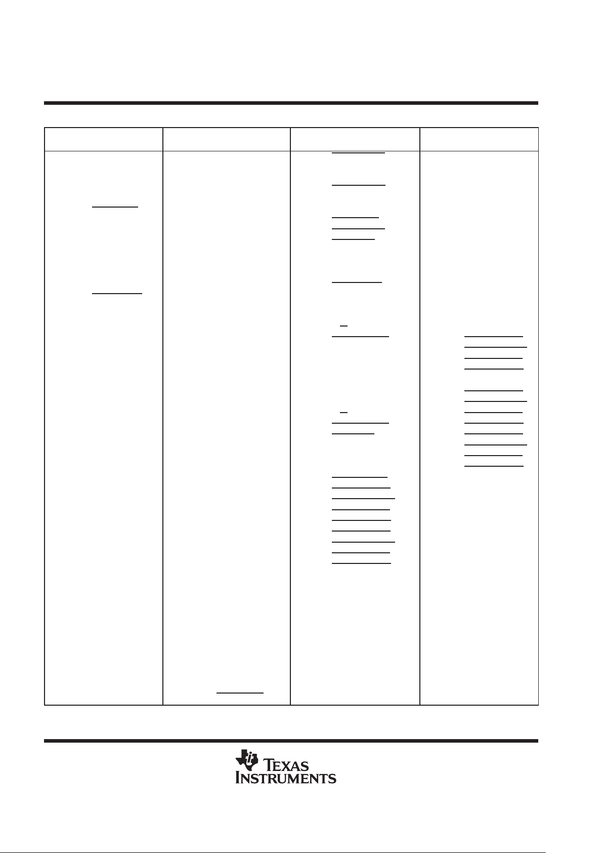
Terminal Assignments
TERMINAL TERMINAL TERMINAL TERMINAL
NO. NAME NO. NAME NO. NAME NO. NAME
1
2
3
4
5
6
7
8
9
10
11
12
13
14
15
16
17
18
19
20
21
22
23
24
25
26
27
28
29
30
31
32
33
34
35
36
37
38
39
40
41
42
43
44
45
46
47
48
49
50
51
ROMEN_C40_#1
IIOF0_C40_#1
IIOF1_C40_#1
IIOF2_C40_#1
IIOF3_C40_#1
NMI_C40_#1
VCC_DR
VSS_CL
TCLK0_C40_#1
TCLK1_C40_#1
H3_C40_#1
H1_C40_#1
VSS_CL
IACK_C40_#1
CLKIN_COMM
VCC_DR
VCC_CL
VCC_DR
VSS_CL
VSS_DR
VCC_DR
VCC_DR
VCC_CL
VSS_CL
VSS_DR
VSS_CL
VCC_DR
A30_C40_#1
A29_C40_#1
A28_C40_#1
VCC_DR
A27_C40_#1
A26_C40_#1
A25_C40_#1
A24_C40_#1
A23_C40_#1
A22_C40_#1
A21_C40_#1
A20_C40_#1
A19_C40_#1
A18_C40_#1
A17_C40_#1
VCC_DR
VSS_CL
VSS_DR
A16_C40_#1
A15_C40_#1
A14_C40_#1
A13_C40_#1
A12_C40_#1
A11_C40_#1
52
53
54
55
56
57
58
59
60
61
62
63
64
65
66
67
68
69
70
71
72
73
74
75
76
77
78
79
80
81
82
83
84
85
86
87
88
89
90
91
92
93
94
95
96
97
98
99
100
101
102
A10_C40_#1
A9_C40_#1
A8_C40_#1
A7_C40_#1
A6_C40_#1
A5_C40_#1
A4_C40_#1
VCC_DR
A3_C40_#1
A2_C40_#1
A1_C40_#1
A0_C40_#1
D31_C40_#2
D30_C40_#2
D29_C40_#2
D28_C40_#2
D27_C40_#2
D26_C40_#2
VCC_DR
D25_C40_#2
D24_C40_#2
D23_C40_#2
D22_C40_#2
D21_C40_#2
D20_C40_#2
D19_C40_#2
D18_C40_#2
D17_C40_#2
D16_C40_#2
VSS_CL
VSS_CL
VCC_DR
VSS_DR
D15_C40_#2
D14_C40_#2
D13_C40_#2
D12_C40_#2
D11_C40_#2
D10_C40_#2
D9_C40_#2
D8_C40_#2
D7_C40_#2
D6_C40_#2
D5_C40_#2
VCC_DR
D4_C40_#2
D3_C40_#2
D2_C40_#2
D1_C40_#2
D0_C40_#2
CE1_C40_#2
103
104
105
106
107
108
109
110
111
112
113
114
115
116
117
118
119
120
121
122
123
124
125
126
127
128
129
130
131
132
133
134
135
136
137
138
139
140
141
142
143
144
145
146
147
148
149
150
151
152
153
RDY1_C40_#2
VSS_DR
VSS_CL
LOCK_C40_#2
VCC_CL
VSS_CL
CE0_C40_#2
RDY0_C40_#2
DE_C40_#2
TCK_COMM
TDO_C40_#2
TMS_COMM
TRST_COMM
EMU0_COMM
EMU1_COMM
PAGE1_C40_#2
R/W
1_C40_#2
STRB1_C40_#2
STAT0_C40_#2
STAT1_C40_#2
VSS_CL
STAT2_C40_#2
STAT3_C40_#2
PAGE0_C40_#2
R/W0_C40_#2
STRB0_C40_#2
AE_C40_#2
RESETLOC1_C40_#2
VCC_DR
RESETLOC0_C40_#2
RESET_COMM
CRDY5_C40_#2
CSTRB5_C40_#2
CACK5_C40_#2
CREQ5_C40_#2
CRDY4_C40_#2
CSTRB4_C40_#2
CACK4_C40_#2
CREQ4_C40_#2
VCC_DR
C5D7_C40_#2
C5D6_C40_#2
C5D5_C40_#2
C5D4_C40_#2
C5D3_C40_#2
C5D2_C40_#2
C5D1_C40_#2
C5D0_C40_#2
VCC_DR
C4D7_C40_#2
C4D6_C40_#2
154
155
156
157
158
159
160
161
162
163
164
165
166
167
168
169
170
171
172
173
174
175
176
177
178
179
180
181
182
183
184
185
186
187
188
189
190
191
192
193
194
195
196
197
198
199
200
201
202
203
204
C4D5_C40_#2
C4D4_C40_#2
C4D3_C40_#2
C4D2_C40_#2
C4D1_C40_#2
C4D0_C40_#2
VCC_DR
VCC_DR
VSS_CL
C2D7_C40_#2
C2D6_C40_#2
C2D5_C40_#2
C2D4_C40_#2
C2D3_C40_#2
C2D2_C40_#2
C2D1_C40_#2
C2D0_C40_#2
CRDY2_C40_#2
CSTRB2_C40_#2
CACK2_C40_#2
CREQ2_C40_#2
VCC_DR
CRDY1_C40_#2
CSTRB1_C40_#2
CACK1_C40_#2
CREQ1_C40_#2
CRDY0_C40_#2
CSTRB0_C40_#2
CACK0_C40_#2
CREQ0_C40_#2
VSS_DR
VSS_CL
VSS_DR
VCC_DR
C1D7_C40_#2
C1D6_C40_#2
C1D5_C40_#2
C1D4_C40_#2
C1D3_C40_#2
C1D2_C40_#2
C1D1_C40_#2
C1D0_C40_#2
VCC_DR
C0D7_C40_#2
C0D6_C40_#2
C0D5_C40_#2
C0D4_C40_#2
C0D3_C40_#2
C0D2_C40_#2
C0D1_C40_#2
C0D0_C40_#2

SMJ320MCM42C, SMJ320MCM42D
DUAL SMJ320C40 MULTICHIP MODULE
SGKS001B – JULY 1997 – REVISED FEBRUARY 2000
5
POST OFFICE BOX 1443 • HOUSTON, TEXAS 77251–1443
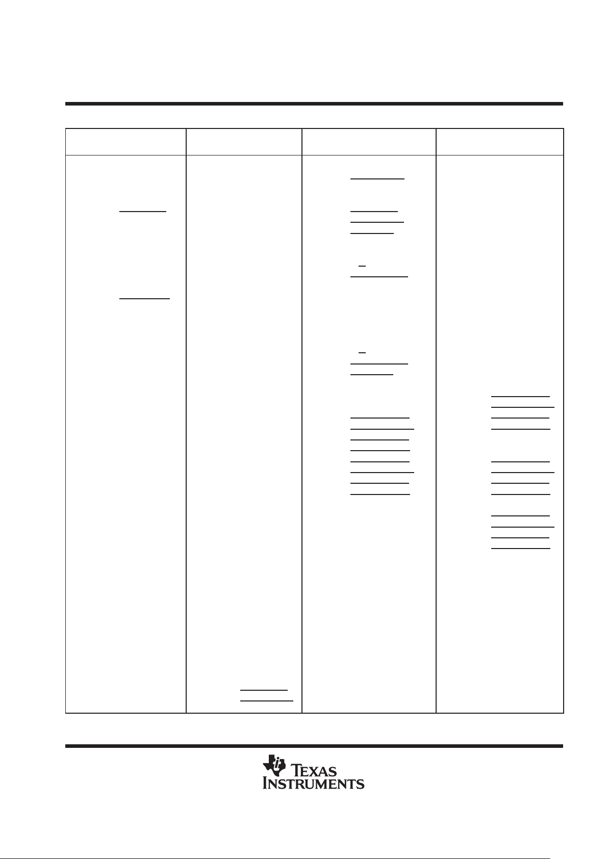
Terminal Assignments (Continued)
TERMINAL TERMINAL TERMINAL TERMINAL
NO. NAME NO. NAME NO. NAME NO. NAME
205
206
207
208
209
210
211
212
213
214
215
216
217
218
219
220
221
222
223
224
225
226
227
228
229
230
231
232
233
234
235
236
237
238
239
240
241
242
243
244
245
246
247
248
249
250
251
252
253
254
255
ROMEN_C40_#2
IIOF0_C40_#2
IIOF1_C40_#2
IIOF2_C40_#2
IIOF3_C40_#2
NMI_C40_#2
VCC_DR
VSS_CL
TCLK0_C40_#2
TCLK1_C40_#2
H3_C40_#2
H1_C40_#2
VSS_CL
IACK_C40_#2
VCC_DR
VCC_DR
VCC_DR
VSS_CL
VSS_DR
VCC_DR
VCC_DR
VCC_CL
VSS_CL
VSS_DR
VSS_CL
VCC_DR
A30_C40_#2
A29_C40_#2
A28_C40_#2
VCC_DR
A27_C40_#2
A26_C40_#2
A25_C40_#2
A24_C40_#2
A23_C40_#2
A22_C40_#2
A21_C40_#2
A20_C40_#2
A19_C40_#2
A18_C40_#2
A17_C40_#2
VCC_DR
VSS_CL
VSS_DR
A16_C40_#2
A15_C40_#2
A14_C40_#2
A13_C40_#2
A12_C40_#2
A11_C40_#2
A10_C40_#2
256
257
258
259
260
261
262
263
264
265
266
267
268
269
270
271
272
273
274
275
276
277
278
279
280
281
282
283
284
285
286
287
288
289
290
291
292
293
294
295
296
297
298
299
300
301
302
303
304
305
306
A9_C40_#2
A8_C40_#2
A7_C40_#2
A6_C40_#2
A5_C40_#2
A4_C40_#2
VCC_DR
A3_C40_#2
A2_C40_#2
A1_C40_#2
A0_C40_#2
D31_C40_#1
D30_C40_#1
D29_C40_#1
D28_C40_#1
D27_C40_#1
D26_C40_#1
VCC_DR
D25_C40_#1
D24_C40_#1
D23_C40_#1
D22_C40_#1
D21_C40_#1
D20_C40_#1
D19_C40_#1
D18_C40_#1
D17_C40_#1
D16_C40_#1
VSS_CL
VSS_CL
VCC_DR
VSS_DR
D15_C40_#1
D14_C40_#1
D13_C40_#1
D12_C40_#1
D11_C40_#1
D10_C40_#1
D9_C40_#1
D8_C40_#1
D7_C40_#1
D6_C40_#1
D5_C40_#1
VCC_DR
D4_C40_#1
D3_C40_#1
D2_C40_#1
D1_C40_#1
D0_C40_#1
CE1_C40_#1
RDY1_C40_#1
307
308
309
310
311
312
313
314
315
316
317
318
319
320
321
322
323
324
325
326
327
328
329
330
331
332
333
334
335
336
337
338
339
340
341
342
343
344
345
346
347
348
349
350
351
352
353
354
355
356
357
VSS_DR
VSS_CL
LOCK_C40_#1
VCC_CL
VSS_CL
CE0_C40_#1
RDY0_C40_#1
DE_C40_#1
TDI_C40_#1
PAGE1_C40_#1
R/W1_C40_#1
STRB1_C40_#1
STAT0_C40_#1
STAT1_C40_#1
VSS_CL
STAT2_C40_#1
STAT3_C40_#1
PAGE0_C40_#1
R/W
0_C40_#1
STRB0_C40_#1
AE_C40_#1
RESETLOC1_C40_#1
VCC_DR
RESETLOC0_C40_#1
CRDY5_C40_#1
CSTRB5_C40_#1
CACK5_C40_#1
CREQ5_C40_#1
CRDY4_C40_#1
CSTRB4_C40_#1
CACK4_C40_#1
CREQ4_C40_#1
VSS_DR
VCC_DR
C5D7_C40_#1
C5D6_C40_#1
C5D5_C40_#1
C5D4_C40_#1
C5D3_C40_#1
C5D2_C40_#1
C5D1_C40_#1
C5D0_C40_#1
VCC_DR
C4D7_C40_#1
C4D6_C40_#1
C4D5_C40_#1
C4D4_C40_#1
C4D3_C40_#1
C4D2_C40_#1
C4D1_C40_#1
C4D0_C40_#1
358
359
360
361
362
363
364
365
366
367
368
369
370
371
372
373
374
375
376
377
378
379
380
381
382
383
384
385
386
387
388
389
390
391
392
393
394
395
396
397
398
399
400
401
402
403
404
405
406
407
408
VSS_DR
VCC_DR
C3D7_C40_#1
C3D6_C40_#1
C3D5_C40_#1
C3D4_C40_#1
C3D3_C40_#1
C3D2_C40_#1
C3D1_C40_#1
C3D0_C40_#1
VCC_DR
VSS_CL
C2D7_C40_#1
C2D6_C40_#1
C2D5_C40_#1
C2D4_C40_#1
C2D3_C40_#1
C2D2_C40_#1
C2D1_C40_#1
C2D0_C40_#1
VSS_DR
VCC_DR
CRDY3_C40_#1
CSTRB3_C40_#1
CACK3_C40_#1
CREQ3_C40_#1
VCC_CL
VSS_CL
CRDY2_C40_#1
CSTRB2_C40_#1
CACK2_C40_#1
CREQ2_C40_#1
VCC_DR
CRDY1_C40_#1
CSTRB1_C40_#1
CACK1_C40_#1
CREQ1_C40_#1
VSS_DR
VSS_CL
VSS_DR
VCC_DR
C1D7_C40_#1
C1D6_C40_#1
C1D5_C40_#1
C1D4_C40_#1
C1D3_C40_#1
C1D2_C40_#1
C1D1_C40_#1
C1D0_C40_#1
VCC_DR
VSS_DR
 Loading...