


SMJ320C80
DIGITAL SIGNAL PROCESSOR
SGUS025 – AUGUST 1998
D
Single-Chip Parallel Multiple
Instruction/Multiple Data (MIMD) Digital
Signal Processor (DSP)
D
More Than Two Billion RISC-Equivalent
Operations per Second
D
Master Processor (MP)
– 32-Bit Reduced Instruction Set
Computing (RISC) Processor
– IEEE-754 Floating-Point Capability
– 4K-Byte Instruction Cache
– 4K-Byte Data Cache
D
Four Parallel Processors (PP)
– 32-Bit Advanced DSPs
– 64-Bit Opcode Provides Many Parallel
Operations per Cycle
– 2K-Byte Instruction Cache and 8K-Byte
Data RAM per PP
D
Transfer Controller (TC)
– 64-Bit Data Transfers
– Up to 400 Megabytes per Second (MBps)
Transfer Rate
– 32-Bit Addressing
– Direct DRAM / VRAM Interface With
Dynamic Bus Sizing
– Intelligent Queuing and Cycle
Prioritization
D
Video Controller (VC)
– Provides Video Timing and Video
Random-Access Memory (VRAM)
Control
– Dual-Frame Timers for Two Simultaneous
Image-Capture and /or Display Systems
D
Big- or Little-Endian Operation
D
50K-Byte On-Chip RAM
D
4G-Byte Address Space
D
20-ns Cycle Time
D
3.3-V Operation
D
IEEE Standard 1149.1† Test Access Port
(JTAG)
D
Military Operating Temperature Range
– 55°C to 125°C
AP
AM
AK
AH
AF
AD
AB
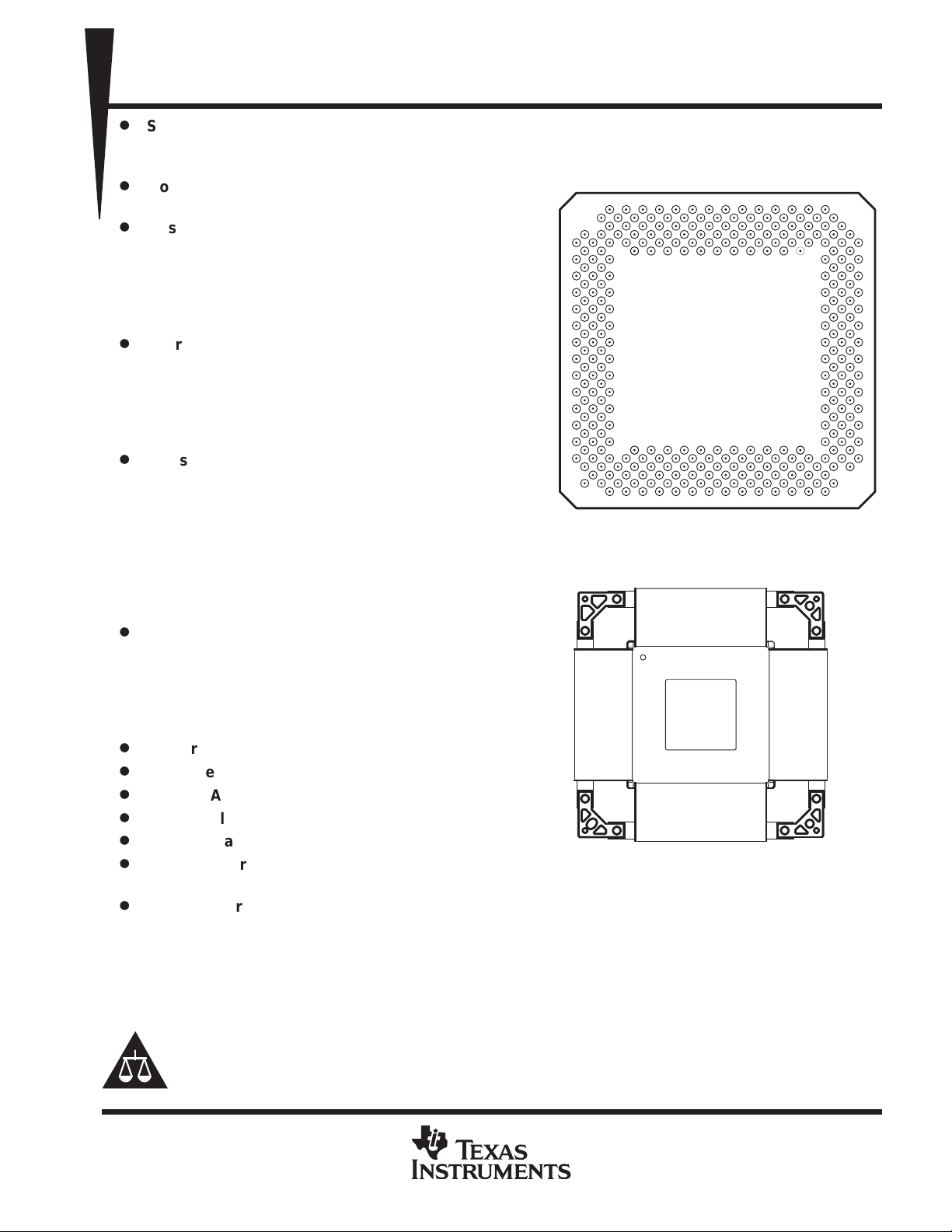
GF PACKAGE
(BOTTOM VIEW)
320
80
10
98765431
HFH PACKAGE
(TOP VIEW)
1
81
35343332313029282726252423222120191817161514131211
241
240
161
160
2
AR
AN
AL
AJ
AG
AE
AC
AA
Y
W
V
U
T
R
P
N
M
L
K
J
H
G
F
E
D
C
B
A
Please be aware that an important notice concerning availability, standard warranty, and use in critical applications of
Texas Instruments semiconductor products and disclaimers thereto appears at the end of this data sheet.
†
IEEE Standard 1149.1–1990, IEEE Standard Test Access Port and Boundary-Scan Architecture
PRODUCTION DATA information is current as of publication date.
Products conform to specifications per the terms of Texas Instruments
standard warranty. Production processing does not necessarily include
testing of all parameters.
POST OFFICE BOX 1443 • HOUSTON, TEXAS 77251–1443
Copyright 1998, Texas Instruments Incorporated
On products compliant to MIL-PRF-38535, all parameters are tested
unless otherwise noted. On all other products, production
processing does not necessarily include testing of all parameters.
1

SMJ320C80
DIGITAL SIGNAL PROCESSOR
SGUS025 – AUGUST 1998
Table of Contents
description 2
GF Pin Assignments – Numerical Listing 3
GF Pin Assignments – Alphabetical Listing 5
HFH Pin Assignments – Numerical Listing 7
HFH Pin Assignments – Alphabetical Listing 9
Terminal Functions 13
architecture 14
master processor (MP) architecture 17
MP control registers 21
MP parameter RAM 28
MP interrupt vectors 29
MP opcode formats 30
MP opcode summary 30
PP architecture 35
PP registers 36
PP data-unit registers 37
PP address-unit registers 37
PP program flow control (PFC) unit registers 38
PP cache architecture 40
PP parameter RAM 41
PP-interrupt vectors 41
PP data unit architecture 42
PP multiplier 43
PP program-flow-control unit architecture 44
PP address-unit architecture 46
PP instruction set 47
PP opcode formats 50
EALU operations 59
TC architecture 61
local memory interface 65
external memory timing examples 71
SDRAM-type cycles 105
special register set cycles 116
device reset 127
absolute maximum ratings over specified temperature
ranges 128
recommended operating conditions 128
electrical characteristics over recommended ranges
of supply voltage and operating case temperature 128
signal transition levels 129
timing parameter symbology 130
general notes on timing parameters 130
CLKIN timing requirements 131
local-bus switching characteristics over full operating
range: CLKOUT 131
device reset timing requirements 132
local bus timing requirements: cycle configuration inputs 133
local bus timing: cycle completion inputs 134
general output signal characteristics over
operating conditions 137
data input timing 139
local bus timing: 2-cycle/column CAS
external interrupt timing 141
XPT input timing 142
host-interface timing 143
video interface timing: SCLK timing 144
video interface timing: FCLK input and video outputs 145
video interface timing: external sync inputs 146
emulator interface connection 147
MECHANICAL DATA 150
MECHANICAL DATA 151
timing 140
description
The SMJ320C80 is a single-chip, MIMD parallel processor capable of performing over two billion operations
per second. It consists of a 32-bit RISC master processor with a 100-MFLOPS (million floating-point operations
per second) IEEE floating-point unit, four 32-bit parallel processing digital signal processors (DSPs), a transfer
controller with up to 400-MBps off-chip transfer rate, and a video controller . All the processors are coupled tightly
through an on-chip crossbar that provides shared access to on-chip RAM. This performance and
programmability make the ’C80 ideally suited for video, imaging, and high-speed telecommunications
applications.
2
POST OFFICE BOX 1443 • HOUSTON, TEXAS 77251–1443
SMJ320C80
DIGITAL SIGNAL PROCESSOR
SGUS025 – AUGUST 1998
GF Pin Assignments – Numerical Listing
PIN PIN PIN PIN
NUMBER NAME NUMBER NAME NUMBER NAME NUMBER NAME
A5 CT1 C21 V
A7 V
A9 HACK C25 DBEN F2 V
A11 V
A13 CAS/DQM7 C29 CAREA0 F8 V
A15 CAS/DQM5 C31 CBLNK0 / VBLNK0 F10 V
A17 V
A19 V
A21 RAS D6 V
A23 DSF D8 AS0 F18 CT2 N3 A8
A25 V
A27 SCLK1 D12 V
A29 V
A31 EINT1 D16 REQ0 F26 V
B2 NC D18 V
B4 BS1 D20 CAS/DQM0 F32 V
B6 V
B8 PS1 D24 V
B10 REQ1 D26 CAREA1 G3 A2 R1 V
B12 V
B14 CAS/DQM6 D30 V
B16 CAS/DQM3 D32 V
B18 V
B20 CAS/DQM1 E1 AS1 H2 STATUS0 R35 V
B22 TRG/CAS E3 FAULT H4 A3 T2 A5
B24 V
B26 DDIN E7 STATUS2 H34 TDI T32 D62
B28 FCLK0 E9 READY J1 STATUS1 T34 EMU0
B30 V
B32 CSYNC0 / HBLNK0 E13 V
C3 V
C5 STATUS3 E17 CAS/DQM4 J33 V
C7 AS2 E19 RL J35 EMU1 U33 D61
C9 V
C11 CT0 E23 V
C13 PS2 E25 CLKOUT K32 VSYNC1 V4 V
C15 V
C17 CLKIN E29 EINT3 L1 A0 V34 V
C19 CAS/DQM2 E31 V
DD
SS
DD
SS
SS
DD
DD
DD
DD
DD
DD
SS
SS
DD
C23 W E35 TCK L31 V
C27 V
D2 RETRY F12 V
D4 V
D10 UTIME F20 V
D14 RESET F24 V
D22 FCLK1 F34 V
D28 SCLK0 G5 A1 R3 V
D34 VSYNC0 G35 V
E5 V
E11 BS0 J3 V
E15 HREQ J31 V
E21 STATUS5 K2 STATUS4 U35 V
E27 LINT4 K34 HSYNC1 V32 V
DD
SS
DD
SS
SS
SS
SS
SS
DD
SS
SS
SS
SS
E33 HSYNC0 L5 V
DD
F4 V
F14 PS0 M34 V
F16 V
F22 V
F28 V
G1 V
G31 EINT2 R5 V
G33 CBLNK1 / VBLNK1 R31 V
H32 CSYNC1 / HBLNK1 T4 A13
J5 V
K4 A6 V2 V
L3 A7 W1 A11
SS
DD
SS
DD
SS
DD
SS
DD
SS
DD
SS
DD
DD
DD
SS
DD
DD
SS
L33 TRST
L35 XPT1
M2 V
M4 V
M32 V
N1 V
N5 V
N31 V
N33 TMS
N35 V
P2 A4
P4 A9
P32 TDO
P34 XPT0
R33 V
U1 V
U3 A10
U5 PS3
U31 NC
SS
SS
DD
SS
SS
DD
DD
SS
SS
DD
SS
DD
DD
DD
DD
SS
DD
DD
DD
SS
SS
DD
POST OFFICE BOX 1443 • HOUSTON, TEXAS 77251–1443
3
SMJ320C80
DIGITAL SIGNAL PROCESSOR
SGUS025 – AUGUST 1998
GF Pin Assignments – Numerical Listing (Continued)
PIN PIN PIN PIN
NUMBER NAME NUMBER NAME NUMBER NAME NUMBER NAME
W3 A18 AG1 A16 AL17 D20 AN29 D35
W5 V
W31 V
W33 D59 AG31 V
W35 D63 AG33 V
Y2 A12 AG35 D57 AL27 D32 AP8 D5
Y4 A19 AH2 A20 AL29 D38 AP10 D8
Y32 XPT2 AH4 A30 AL31 V
Y34 D56 AH32 D44 AL33 D48 AP14 D13
AA1 V
AA3 V
AA5 V
AA31 V
AA33 V
AA35 V
AB2 A14 AJ35 V
AB4 A21 AK2 V
AB32 D55 AK4 V
AB34 D60 AK8 V
AC1 V
AC3 A22 AK12 V
AC5 V
AC31 V
AC33 D52 AK18 NC AM28 D33 AR15 D15
AC35 V
AD2 V
AD4 V
AD32 V
AD34 V
AE1 A15 AK32 V
AE3 A26 AK34 V
AE5 V
AE31 V
AE33 D51 AL5 V
AE35 D58 AL7 D3 AN19 D22
AF2 A17 AL9 D4 AN21 V
AF4 A28 AL11 D10 AN23 D28
AF32 D46 AL13 V
AF34 D49 AL15 D16 AN27 V
SS
SS
SS
DD
DD
DD
DD
SS
DD
SS
SS
DD
DD
SS
SS
DD
SS
SS
AG3 V
AG5 V
AH34 D54 AL35 D53 AP16 D17
AJ1 V
AJ3 A31 AM4 V
AJ5 V
AJ31 V
AJ33 D42 AM10 D6 AP26 D39
AK10 V
AK14 V
AK16 V
AK20 V
AK22 D27 AM32 V
AK24 V
AK26 V
AK28 V
AL1 A23 AN13 D12 AR31 D43
AL3 A25 AN15 V
SS
DD
DD
SS
DD
SS
SS
DD
DD
SS
DD
SS
DD
SS
DD
SS
DD
SS
DD
SS
DD
SS
SS
AL19 D21 AN31 D45
AL21 D24 AN33 V
AL23 V
AL25 D29 AP6 V
AM2 A24 AP18 V
AM6 V
AM8 D2 AP24 V
AM12 V
AM14 D14 AP30 V
AM16 D19 AP32 D47
AM18 V
AM20 D23 AR7 V
AM22 D25 AR9 D7
AM24 V
AM26 D31 AR13 D11
AM30 V
AM34 D50 AR21 D30
AN5 A29 AR23 D36
AN7 D1 AR25 V
AN9 V
AN11 D9 AR29 V
AN17 D18
AN25 D37
SS
SS
DD
SS
SS
SS
SS
SS
DD
SS
DD
DD
SS
AP4 A27
AP12 V
AP20 D26
AP22 D34
AP28 D41
AR5 D0
AR11 V
AR17 V
AR19 V
AR27 D40
DD
DD
DD
DD
DD
DD
DD
SS
SS
DD
SS
DD
4
POST OFFICE BOX 1443 • HOUSTON, TEXAS 77251–1443
SMJ320C80
DIGITAL SIGNAL PROCESSOR
SGUS025 – AUGUST 1998
GF Pin Assignments – Alphabetical Listing
PIN PIN PIN PIN
NAME NUMBER NAME NUMBER NAME NUMBER NAME NUMBER
A0 L1 CAS/DQM1 B20 D24 AL21 DBEN C25
A1 G5 CAS/DQM2 C19 D25 AM22 DDIN B26
A2 G3 CAS/DQM3 B16 D26 AP20 DSF A23
A3 H4 CAS/DQM4 E17 D27 AK22 EINT1 A31
A4 P2 CAS/DQM5 A15 D28 AN23 EINT2 G31
A5 T2 CAS/DQM6 B14 D29 AL25 EINT3 E29
A6 K4 CAS/DQM7 A13 D30 AR21 EMU0 T34
A7 L3 CBLNK0/VBLNK0 C31 D31 AM26 EMU1 J35
A8 N3 CBLNK1/VBLNK1 G33 D32 AL27 FAULT E3
A9 P4 CLKIN C17 D33 AM28 FCLK0 B28
A10 U3 CLKOUT E25 D34 AP22 FCLK1 D22
A11 W1 CSYNC0/HBLNK0 B32 D35 AN29 HACK A9
A12 Y2 CSYNC1/HBLNK1 H32 D36 AR23 HREQ E15
A13 T4 CT0 C11 D37 AN25 HSYNC0 E33
A14 AB2 CT1 A5 D38 AL29 HSYNC1 K34
A15 AE1 CT2 F18 D39 AP26 LINT4 E27
A16 AG1 D0 AR5 D40 AR27 NC B2
A17 AF2 D1 AN7 D41 AP28 NC U31
A18 W3 D2 AM8 D42 AJ33 NC AK18
A19 Y4 D3 AL7 D43 AR31 PS0 F14
A20 AH2 D4 AL9 D44 AH32 PS1 B8
A21 AB4 D5 AP8 D45 AN31 PS2 C13
A22 AC3 D6 AM10 D46 AF32 PS3 U5
A23 AL1 D7 AR9 D47 AP32 RAS A21
A24 AM2 D8 AP10 D48 AL33 READY E9
A25 AL3 D9 AN11 D49 AF34 REQ0 D16
A26 AE3 D10 AL11 D50 AM34 REQ1 B10
A27 AP4 D11 AR13 D51 AE33 RESET D14
A28 AF4 D12 AN13 D52 AC33 RETRY D2
A29 AN5 D13 AP14 D53 AL35 RL E19
A30 AH4 D14 AM14 D54 AH34 SCLK0 D28
A31 AJ3 D15 AR15 D55 AB32 SCLK1 A27
AS0 D8 D16 AL15 D56 Y34 STATUS0 H2
AS1 E1 D17 AP16 D57 AG35 STATUS1 J1
AS2 C7 D18 AN17 D58 AE35 STATUS2 E7
BS0 E11 D19 AM16 D59 W33 STATUS3 C5
BS1 B4 D20 AL17 D60 AB34 STATUS4 K2
CAREA0 C29 D21 AL19 D61 U33
CAREA1 D26 D22 AN19 D62 T32
CAS/DQM0 D20 D23 AM20 D63 W35
POST OFFICE BOX 1443 • HOUSTON, TEXAS 77251–1443
5
SMJ320C80
DIGITAL SIGNAL PROCESSOR
SGUS025 – AUGUST 1998
GF Pin Assignments – Alphabetical Listing (Continued)
PIN PIN PIN PIN
NAME NUMBER NAME NUMBER NAME NUMBER NAME NUMBER
STATUS5 E21 V
TCK E35 V
TDI H34 V
TDO P32 V
TMS N33 V
TRG/CAS B22 V
TRST L33 V
UTIME D10 V
V
DD
V
DD
V
DD
V
DD
V
DD
V
DD
V
DD
V
DD
V
DD
V
DD
V
DD
V
DD
V
DD
V
DD
V
DD
V
DD
V
DD
V
DD
V
DD
V
DD
V
DD
V
DD
V
DD
V
DD
V
DD
V
DD
V
DD
V
DD
V
DD
A7 V
A17 V
A29 V
B6 V
B12 V
B18 V
B24 V
B30 V
C15 V
C21 V
D4 V
D32 V
F2 V
F8 V
F12 V
F20 V
F24 V
F28 V
F34 V
G1 V
G35 V
J5 V
J31 V
M2 V
M34 V
N1 V
N35 V
R3 V
R5 V
DD
DD
DD
DD
DD
DD
DD
DD
DD
DD
DD
DD
DD
DD
DD
DD
DD
DD
DD
DD
DD
DD
DD
DD
DD
DD
DD
DD
DD
DD
DD
DD
DD
DD
DD
DD
DD
R31 V
R33 V
U1 V
U35 V
V2 V
V34 V
AA3 V
AA5 V
AA31 V
AA33 V
AC1 V
AC35 V
AD2 V
AD34 V
AG5 V
AG31 V
AJ1 V
AJ35 V
AK2 V
AK8 V
AK12 V
AK16 V
AK24 V
AK28 V
AK34 V
AM4 V
AM32 V
AN15 V
AN21 V
AN33 V
AP6 V
AP12 V
AP18 V
AP24 V
AP30 V
AR7 V
AR19 V
DD
SS
SS
SS
SS
SS
SS
SS
SS
SS
SS
SS
SS
SS
SS
SS
SS
SS
SS
SS
SS
SS
SS
SS
SS
SS
SS
SS
SS
SS
SS
SS
SS
SS
SS
SS
SS
AR29 V
A11 V
A19 V
A25 V
C3 V
C9 V
C27 V
D6 V
D12 V
D18 V
D24 V
D30 V
E5 V
E13 V
E23 V
E31 V
F4 V
F10 V
F16 V
F22 V
F26 V
F32 V
J3 V
J33 V
L5 V
L31 V
M4 V
M32 V
N5 V
N31 V
R1 V
R35 VSYNC0 D34
V4 VSYNC1 K32
V32 W C23
W5 XPT0 P34
W31 XPT1 L35
AA1 XPT2 Y32
SS
SS
SS
SS
SS
SS
SS
SS
SS
SS
SS
SS
SS
SS
SS
SS
SS
SS
SS
SS
SS
SS
SS
SS
SS
SS
SS
SS
SS
SS
SS
AA35
AC5
AC31
AD4
AD32
AE5
AE31
AG3
AG33
AJ5
AJ31
AK4
AK10
AK14
AK20
AK26
AK32
AL5
AL13
AL23
AL31
AM6
AM12
AM18
AM24
AM30
AN9
AN27
AR11
AR17
AR25
6
POST OFFICE BOX 1443 • HOUSTON, TEXAS 77251–1443
SMJ320C80
DIGITAL SIGNAL PROCESSOR
SGUS025 – AUGUST 1998
HFH Pin Assignments – Numerical Listing
PIN PIN PIN PIN
NUMBER NAME NUMBER NAME NUMBER NAME NUMBER NAME
1 STATUS3 41 CAS/DQM6 81 LINT4 121 V
2 V
3 STATUS2 43 CAS/DQM5 83 EINT2 123 V
4 STATUS1 44 V
5 V
6 STATUS0 46 CAS/DQM3 86 CBLNK0/VBLNK0 126 D57
7 AS2 47 CT2 87 V
8 AS1 48 CAS/DQM2 88 V
9 AS0 49 V
10 FAULT 50 CAS/DQM1 90 V
11 READY 51 V
12 RETRY 52 CAS/DQM0 92 CSYNC0/HBLNK0 132 D55
13 UTIME 53 RL 93 VSYNC1 133 V
14 BS1 54 RAS 94 VSYNC0 134 D54
15 BS0 55 V
16 CT1 56 V
17 CT0 57 V
18 PS2 58 TRG/CAS 98 V
19 PS1 59 V
20 PS0 60 FCLK1 100 V
21 V
22 RESET 62 V
23 V
24 HREQ 64 STATUS5 104 TMS 144 V
25 HACK 65 V
26 V
27 V
28 REQ1 68 DBEN 108 XPT0 148 V
29 REQ0 69 V
30 V
31 V
32 V
33 V
34 V
35 V
36 CLKIN 76 FCLK0 116 V
37 V
38 CAS/DQM7 78 SCLK0 118 V
39 V
40 V
SS
DD
DD
SS
SS
SS
DD
DD
SS
DD
SS
SS
SS
DD
DD
42 V
45 CAS/DQM4 85 CBLNK1/VBLNK1 125 V
61 V
63 W 103 TCK 143 D49
66 DSF 106 TDO 146 D48
67 V
70 DDIN 110 V
71 CLKOUT 111 V
72 CAREA1 112 EMU0 152 D45
73 V
74 SCLK1 114 D63 154 V
75 V
77 V
79 V
80 CAREA0 120 V
SS
DD
SS
DD
SS
SS
SS
DD
DD
DD
DD
SS
DD
SS
DD
SS
DD
82 EINT3 122 D59
84 EINT1 124 D58
SS
SS
89 CSYNC1/HBLNK1 129 D56
DD
91 V
95 V
96 V
97 HSYNC1 137 V
99 V
101 HSYNC0 141 D51
102 TRST 142 D50
105 TDI 145 V
107 EMU1 147 V
109 XPT1 149 V
113 V
115 D62 155 D44
117 D61 157 V
119 D60 159 D43
DD
SS
SS
DD
DD
DD
SS
SS
DD
SS
SS
DD
127 XPT2
128 V
130 V
131 V
135 V
136 D53
138 V
139 D52
140 V
150 D47
151 D46
153 V
156 V
158 V
160 D42
DD
SS
DD
SS
DD
DD
SS
DD
SS
SS
DD
SS
SS
DD
DD
DD
SS
SS
DD
DD
DD
POST OFFICE BOX 1443 • HOUSTON, TEXAS 77251–1443
7
SMJ320C80
DIGITAL SIGNAL PROCESSOR
SGUS025 – AUGUST 1998
HFH Pin Assignments – Numerical Listing (Continued)
PIN PIN PIN
NUMBER NAME NUMBER NAME NUMBER NAME NUMBER NAME
161 D41 201 D20 241 D0 281 V
162 V
163 V
164 D40 204 D19 244 A31 284 A15
165 V
166 D39 206 D18 246 A30 286 A14
167 D38 207 V
168 D37 208 D17 248 V
169 V
170 D36 210 V
171 V
172 V
173 D35 213 D15 253 V
174 D34 214 D14 254 A27 294 A11
175 D33 215 D13 255 A26 295 V
176 V
177 D32 217 V
178 V
179 V
180 D31 220 V
181 D30 221 V
182 D29 222 D11 262 V
183 V
184 V
185 V
186 D28 226 D8 266 V
187 V
188 V
189 D27 229 D7 269 V
190 D26 230 D6 270 A20 310 V
191 D25 231 D5 271 V
192 V
193 D24 233 V
194 V
195 V
196 D23 236 D3 276 A17 316 A1
197 D22 237 D2 277 V
198 V
199 D21 239 D1 279 V
200 V
SS
SS
DD
SS
SS
DD
SS
DD
DD
SS
SS
SS
DD
DD
SS
DD
DD
SS
SS
202 V
203 V
205 V
209 V
211 D16 251 V
212 V
216 V
218 D12 258 V
219 V
223 D10 263 V
224 D9 264 A23 304 V
225 V
227 V
228 V
232 V
234 D4 274 V
235 V
238 V
240 V
DD
DD
DD
SS
SS
SS
DD
SS
SS
DD
DD
DD
SS
DD
DD
SS
SS
DD
SS
SS
242 V
243 V
245 V
247 A29 287 V
249 V
250 A28 290 V
252 V
256 A25 296 A10
257 V
259 V
260 A24 300 A8
261 V
265 A22 305 V
267 A21 307 V
268 V
272 V
273 A19 313 V
275 A18 315 V
278 V
280 A16 320 V
DD
DD
SS
SS
SS
DD
DD
DD
SS
SS
SS
DD
DD
DD
DD
SS
SS
DD
DD
SS
SS
SS
SS
282 V
283 V
285 PS3
288 V
289 A13
291 V
292 A12
293 V
297 V
298 A9
299 V
301 V
302 A7
303 A6
306 A5
308 A4
309 V
311 V
312 A3
314 A2
317 A0
318 V
319 STATUS4
DD
DD
DD
SS
DD
SS
SS
DD
SS
DD
SS
DD
SS
SS
SS
DD
DD
DD
DD
SS
DD
SS
8
POST OFFICE BOX 1443 • HOUSTON, TEXAS 77251–1443
DIGITAL SIGNAL PROCESSOR
SGUS025 – AUGUST 1998
HFH Pin Assignments – Alphabetical Listing
PIN PIN PIN PIN
NAME NUMBER NAME NUMBER NAME NUMBER NAME NUMBER
A0 317 CAS/DQM1 50 D30 181 DBEN 68
A1 316 CAS/DQM2 48 D31 180 DDIN 70
A10 296 CAS/DQM3 46 D32 177 DSF 66
A11 294 CAS/DQM4 45 D33 175 EINT1 84
A12 292 CAS/DQM5 43 D34 174 EINT2 83
A13 289 CAS/DQM6 41 D35 173 EINT3 82
A14 286 CAS/DQM7 38 D36 170 EMU0 112
A15 284 CBLNK0/VBLNK0 86 D37 168 EMU1 107
A16 280 CBLNK1/VBLNK1 85 D38 167 FAULT 10
A17 276 CLKIN 36 D39 166 FCLK0 76
A18 275 CLKOUT 71 D4 234 FCLK1 60
A19 273 CSYNC0/HBLNK0 92 D40 164 HACK 25
A2 314 CSYNC1/HBLNK1 89 D41 161 HREQ 24
A20 270 CT0 17 D42 160 HSYNC0 101
A21 267 CT1 16 D43 159 HSYNC1 97
A22 265 CT2 47 D44 155 LINT4 81
A23 264 D0 241 D45 152 PS0 20
A24 260 D1 239 D46 151 PS1 19
A25 256 D10 223 D47 150 PS2 18
A26 255 D11 222 D48 146 PS3 285
A27 254 D12 218 D49 143 RAS 54
A28 250 D13 215 D5 231 READY 11
A29 247 D14 214 D50 142 REQ0 29
A3 312 D15 213 D51 141 REQ1 28
A30 246 D16 211 D52 139 RESET 22
A31 244 D17 208 D53 136 RETRY 12
A4 308 D18 206 D54 134 RL 53
A5 306 D19 204 D55 132 SCLK0 78
A6 303 D2 237 D56 129 SCLK1 74
A7 302 D20 201 D57 126 STATUS0 6
A8 300 D21 199 D58 124 STATUS1 4
A9 298 D22 197 D59 122 STATUS2 3
AS0 9 D23 196 D6 230 STATUS3 1
AS1 8 D24 193 D60 119 STATUS4 319
AS2 7 D25 191 D61 117 STATUS5 64
BS0 15 D26 190 D62 115 TCK 103
BS1 14 D27 189 D63 114 TDI 105
CAREA0 80 D28 186 D7 229
CAREA1 72 D29 182 D8 226
CAS/DQM0 52 D3 236 D9 224
SMJ320C80
POST OFFICE BOX 1443 • HOUSTON, TEXAS 77251–1443
9

SMJ320C80
DIGITAL SIGNAL PROCESSOR
SGUS025 – AUGUST 1998
HFH Pin Assignments – Alphabetical Listing (Continued)
PIN PIN PIN PIN
NAME NUMBER NAME NUMBER NAME NUMBER NAME NUMBER
TDO 106 V
TMS 104 V
TRG/CAS 58 V
TRST 102 V
UTIME 13 V
V
DD
V
DD
V
DD
V
DD
V
DD
V
DD
V
DD
V
DD
V
DD
V
DD
V
DD
V
DD
V
DD
V
DD
V
DD
V
DD
V
DD
V
DD
V
DD
V
DD
V
DD
V
DD
V
DD
V
DD
V
DD
V
DD
V
DD
V
DD
V
DD
V
DD
V
DD
V
DD
V
DD
V
DD
V
DD
V
DD
100 V
113 V
120 V
121 V
125 V
130 V
131 V
135 V
140 V
147 V
148 V
149 V
156 V
157 V
158 V
165 V
172 V
178 V
179 V
187 V
188 V
194 V
195 V
202 V
203 V
205 V
21 V
212 V
219 V
220 V
221 V
227 V
228 V
235 V
31 V
242 V
DD
DD
DD
DD
DD
DD
DD
DD
DD
DD
DD
DD
DD
DD
DD
DD
DD
DD
DD
DD
DD
DD
DD
DD
DD
DD
DD
DD
DD
DD
DD
DD
DD
DD
DD
DD
DD
DD
DD
DD
SS
243 V
251 V
252 V
253 V
261 V
262 V
263 V
266 V
271 V
272 V
281 V
282 V
283 V
288 V
293 V
297 V
30 V
301 V
309 V
310 V
311 V
313 V
318 V
39 V
40 V
33 V
44 V
5 V
51 V
59 V
61 V
62 V
65 V
69 V
75 V
79 V
90 V
91 V
98 V
99 V
32 V
SS
SS
SS
SS
SS
SS
SS
SS
SS
SS
SS
SS
SS
SS
SS
SS
SS
SS
SS
SS
SS
SS
SS
SS
SS
SS
SS
SS
SS
SS
SS
SS
SS
SS
SS
SS
SS
SS
SS
SS
SS
110 V
111 V
116 V
118 V
123 V
128 V
133 V
137 V
138 V
144 V
145 V
153 V
154 V
162 V
163 V
169 V
171 V
176 V
183 V
184 V
185 V
192 V
198 V
2 V
200 V
207 V
209 V
216 V
217 V
225 V
23 V
232 V
233 V
238 V
240 VSYNC0 94
245 VSYNC1 93
248 W 63
249 XPT0 108
257 XPT1 109
210 XPT2 127
258
SS
SS
SS
SS
SS
SS
SS
SS
SS
SS
SS
SS
SS
SS
SS
SS
SS
SS
SS
SS
SS
SS
SS
SS
SS
SS
SS
SS
SS
SS
SS
SS
SS
SS
259
26
268
269
27
274
277
278
279
287
290
291
295
299
304
305
307
315
320
34
35
37
42
49
55
56
57
67
73
77
87
88
95
96
10
POST OFFICE BOX 1443 • HOUSTON, TEXAS 77251–1443
DESCRIPTION
SMJ320C80
DIGITAL SIGNAL PROCESSOR
SGUS025 – AUGUST 1998
Terminal Functions
TERMINAL
NAME TYPE
A31–A0 O
AS2–AS0 I
BS1–BS0 I
CT2–CT0 I Cycle timing selection. CT2–CT0 signals determine the timing of the current memory access.
D63–D0 I/O Data bus. D63–D0 transfer up to 64 bits of data per memory cycle into or out of the ’C80.
DBEN O
DDIN O
FAULT I
PS3–PS0 I
READY I
RL O
RETRY I
STATUS5–STATUS0 O
UTIME I
CAS/DQM7–
CAS
/DQM0
DSF O
RAS O Row-address strobe. RAS drives the RAS inputs of DRAMs, VRAMs, and SDRAMs.
TRG/CAS O
W O
†
I = input, O = output, Z = high-impedance
‡
This pin has an internal pullup and can be left unconnected during normal operation.
§
This pin has an internal pulldown and can be left unconnected during normal operation.
¶
For proper operation, all VDD and VSS pins must be connected externally.
†
LOCAL MEMORY INTERFACE
Address bus. A31–A0 output the 32-bit byte address of the external memory cycle. The address can be
multiplexed for DRAM accesses.
Address-shift selection. AS2–AS0 determine how the column address appears on the address bus. Eight
shift values are supported, including zero.
Bus size selection. BS1 – BS0 indicate the bus size of the memory or other devices being accessed,
allowing dynamic bus sizing for data buses less than 64 bits wide.
Data-buffer enable. DBEN drives the active-low output enables of bidirectional transceivers that can be
used to buffer input and output data on D63–D0.
Data direction indicator. DDIN indicates the direction of the data that passes through the transceivers.
When DDIN
Fault. FAULT is driven low by external circuitry to inform the ’C80 that a fault has occurred on the current
memory row access.
Page size indication. PS3– PS0 indicate the page size of the memory device(s) being accessed by the
current cycle. The ’C80 uses this information to determine when to begin a new row access.
Ready. READY indicates that the external device is ready to complete the memory cycle. READY is driven
low by external circuitry to insert wait states into a memory cycle.
Row latch. The high-to-low transition of RL can be used to latch the valid 32-bit byte address that is present
on A31–A0.
Retry. RETR Y is driven low by external circuitry to indicate that the addressed memory is busy. The ’C80
memory cycle is rescheduled.
Status code. At row time, STA TUS5–STATUS0 indicate the type of cycle being performed. At column time,
they identify the processor and type of request that initiated the cycle.
User-timing selection. UTIME causes the timing of RAS and CAS/DQM7–CAS/DQM0 to be modified so
that custom memory timings can be generated. During reset, UTIME
’C80 operates.
Column-address strobes. CAS/DQM7–CAS/DQM0 drive the CAS inputs of DRAMs and VRAMs, or the
DQM input of synchronous dynamic random-access memories (SDRAMs). The eight strobes provide
O
byte-write access to memory.
Special function. DSF selects special VRAM functions such as block-write, load color register , split-register
transfer, and synchronous graphics random-access memory (SGRAM) block write.
Transfer/output enable or column-address strobe. TRG/CAS is used as an output enable for DRAMs and
VRAMs, and also as a transfer enable for VRAMs. TRG
Write enable. W is driven low before CAS during write cycles. W controls the direction of the transfer during
VRAM transfer cycles.
is low, the transfer is from external memory into the ’C80.
selects the endian mode in which the
DRAM, VRAM, AND SDRAM CONTROL
/CAS also drives the CAS inputs of SDRAMs.
POST OFFICE BOX 1443 • HOUSTON, TEXAS 77251–1443
11
SMJ320C80
DIGITAL SIGNAL PROCESSOR
SGUS025 – AUGUST 1998
Terminal Functions (Continued)
TERMINAL
NAME
HACK O
HREQ I
REQ1, REQ0 O
CLKIN I
CLKOUT O
EINT1, EINT2, EINT3 I
LINT4 I
RESET I
XPT2–XPT0 I
EMU0, EMU1
‡
TCK
‡
TDI
TDO O Test data output. TDO provides output data for all IEEE-1149.1 instructions and data scans of the ’C80.
‡
TMS
TRST
†
I = input, O = output, Z = high-impedance
‡
This pin has an internal pullup and can be left unconnected during normal operation.
§
This pin has an internal pulldown and can be left unconnected during normal operation.
¶
For proper operation, all VDD and VSS pins must be connected externally.
‡
§
†
TYPE
HOST INTERFACE
Host acknowledge. The ’C80 drives HACK output low following an active HREQ to indicate that it has driven
the local memory bus signals to the high-impedance state and is relinquishing the bus. HACK
asynchronously following HREQ
Host request. An external device drives HREQ low to request ownership of the local memory bus. When
HREQ
is high, the ’C80 owns and drives the bus. HREQ is synchronized internally to the ’C80’s internal
clock. Also, HREQ
edge of RESET
occurrence on EINT3
Internal cycle request. REQ1 and REQ0 provide a two-bit code indicating the highest-priority memory cycle
request that is being received by the TC. External logic can monitor REQ1 and REQ0 to determine if it is
necessary to relinquish the local memory bus to the ’C80.
Input clock. CLKIN generates the internal ’C80 clocks to which all processor functions (except the frame
timers) are synchronous.
Local output clock. CLKOUT provides a way to synchronize external circuitry to internal timings. All ’C80
output signals (except the VC signals) are synchronous to this clock.
Edge-triggered interrupts. EINT1, EINT2 and EINT3 allow external devices to interrupt the master
processor (MP) on one of three interrupt levels (EINT1
triggered. EINT3
EINT3
causes the MP to unhalt and fetch its reset vector (the EINT3 interrupt-pending bit is not set in this
case).
Level-triggered interrupt. LINT4 provides an active-low level-triggered interrupt to the MP. Its priority falls
below that of the edge-triggered interrupts. Any interrupt request should remain low until it is recognized
by the ’C80.
Reset. RESET is driven low to reset the ’C80 (all processors). During reset, all internal registers are set
to their initial state and all outputs are driven to their inactive or high-impedance levels. During the rising
edge of RESET
of HREQ
External packet transfer. XPT2–XPT0 are used by external devices to request a high-priority XPT by the
TC.
I/O
Emulation pins. EMU0 and EMU1 are used to support emulation host interrupts, special functions targeted
at a single processor, and multiprocessor halt-event communications.
Test clock. TCK provides the clock for the ’C80 IEEE-1149.1 logic, allowing it to be compatible with other
I
IEEE-1149.1 devices, controllers, and test equipment designed for different clock rates.
I Test data input. TDI provides input data for all IEEE-1149.1 instructions and data scans of the ’C80.
I Test-mode select. TMS controls the IEEE-1149.1 state machine.
Test reset. TRST resets the ’C80 IEEE-1149.1 module. When low, all boundary-scan logic is disabled,
I
allowing normal ’C80 operation.
and UTIME pins, respectively.
is used at reset to determine the power-up state of the MP . If HREQ is low at the rising
, the MP comes up running. If HREQ is high, the MP remains halted until the first interrupt
.
SYSTEM CONTROL
also serves as an unhalt signal. If the MP is powered-up halted, the first rising edge on
, the MP reset mode and the ’C80’s operating endian mode are determined by the levels
EMULATION CONTROL
being detected inactive, and then the ’C80 resumes driving the bus.
DESCRIPTION
DESCRIPTION
is the highest priority). The interrupts are rising-edge
is driven high
12
POST OFFICE BOX 1443 • HOUSTON, TEXAS 77251–1443
SMJ320C80
DIGITAL SIGNAL PROCESSOR
SGUS025 – AUGUST 1998
Terminal Functions (Continued)
TERMINAL
NAME
CAREA0, CAREA1 O
CBLNK0 / VBLNK0,
CBLNK1
CSYNC0 / HBLNK0,
CSYNC1
FCLK0, FCLK1 I
HSYNC0,
HSYNC1
SCLK0, SCLK1 I
VSYNC0,
VSYNC1
V
V
†
‡
§
¶
/ VBLNK1
/ HBLNK1
¶
SS
¶
DD
I = input, O = output, Z = high-impedance
This pin has an internal pullup and can be left unconnected during normal operation.
This pin has an internal pulldown and can be left unconnected during normal operation.
For proper operation, all VDD and VSS pins must be connected externally.
†
TYPE
VIDEO INTERFACE
Composite area. CAREA0 and CAREA1 define a special area such as an overscan boundary. This area
represents the logical OR of the internal horizontal and vertical area signals.
Composite blanking/vertical blanking. Each of CBLNK0 / VBLNK0 and CBLNK1/VBLNK1 provides one
of two blanking functions, depending on the configuration of the CSYNC
Composite blanking disables pixel display/capture during both horizontal and vertical retrace periods
O
I/O/Z
I/O/Z
I/O/Z
I Ground. Electrical ground inputs
I Power. Nominal 3.3-V power supply inputs
and is enabled when CSYNC is selected for composite-sync video systems.
Vertical blanking disables pixel display/capture during vertical retrace periods and is enabled when
HBLNK
is selected for separate-sync video systems.
Following reset, CBLNK0
respectively.
Composite sync /horizontal blanking. CSYNC0 / HBLNK0 and CSYNC1 / HBLNK1 can be programmed
for one of two functions:
Composite sync is for use on composite-sync video systems and can be programmed as an input,
output, or high-impedance signal
from externally generated active-low sync pulses. As an output, the active-low composite-sync pulses
are generated from either external HSYNC
the high-impedance state, the pin is neither driven nor allowed to drive circuitry.
Horizontal blank disables pixel display / capture during horizontal retrace periods in separate-sync
video systems and can be used as an output only.
Immediately following reset, CSYNC0
high-impedance CSYNC0
Frame clock. FCLK0 and FCLK1 are derived from the external video system’s dotclock and are used to
drive the ’C80 video logic for frame timer 0 and frame timer 1.
Horizontal sync. HSYNC0 and HSYNC1 control the video system. They can be programmed as input,
output, or high impedance signals. As an input, HSYNC
generated horizontal sync pulses. As an output, HSYNC
by the ’C80 on-chip frame timer. In the high-impedance state, the pin is not driven, and no internal
synchronization is allowed to occur. Immediately following reset, HSYNC0
high-impedance state.
Serial data clock. SCLK0 and SCLK1 are used by the ’C80 shift register transfer (SRT) controller to track
the VRAM tap point when using midline reload. SCLK0 and SCLK1 should be the same signals that clock
the serial register on the VRAMs controlled by frame timer 0 and frame timer 1, respectively.
Vertical sync. VSYNC0 and VSYNC1 control the video system. They can be programmed as inputs,
outputs, or high-impedance signals. As inputs, VSYNCx
generated vertical-sync pulses. As outputs, VSYNCx
’C80 on-chip frame timer. In the high-impedance state, the pin is not driven and no internal synchronization
is allowed to occur. Immediately following reset, VSYNCx
/ VBLNK0 and CBLNK1 / VBLNK1 are configured as CBLNK0 and CBLNK1,
and CSYNC1, respectively.
POWER
DESCRIPTION
DESCRIPTION
. As an input, the ’C80 extracts horizontal and vertical sync information
and VSYNC signals or the ’C80’s internal video timers. In
/ HBLNK0 and CSYNC1 / HBLNK1 are configured as
/HBLNK pin:
synchronizes the video timer to externally
is an active-low horizontal sync pulse generated
and HSYNC1 are in the
synchronize the frame timer to externally
are active-low vertical-sync pulses generated by the
is in the high-impedance state.
POST OFFICE BOX 1443 • HOUSTON, TEXAS 77251–1443
13

SMJ320C80
DIGITAL SIGNAL PROCESSOR
SGUS025 – AUGUST 1998
Terminal Functions (Continued)
TERMINAL
NAME
NC No connect serves as an alignment key or is for factory use and must be left unconnected.
†
I = input, O = output, Z = high-impedance
‡
This pin has an internal pullup and can be left unconnected during normal operation.
§
This pin has an internal pulldown and can be left unconnected during normal operation.
¶
For proper operation, all VDD and VSS pins must be connected externally.
TYPE
†
MISCELLANEOUS
DESCRIPTION
DESCRIPTION
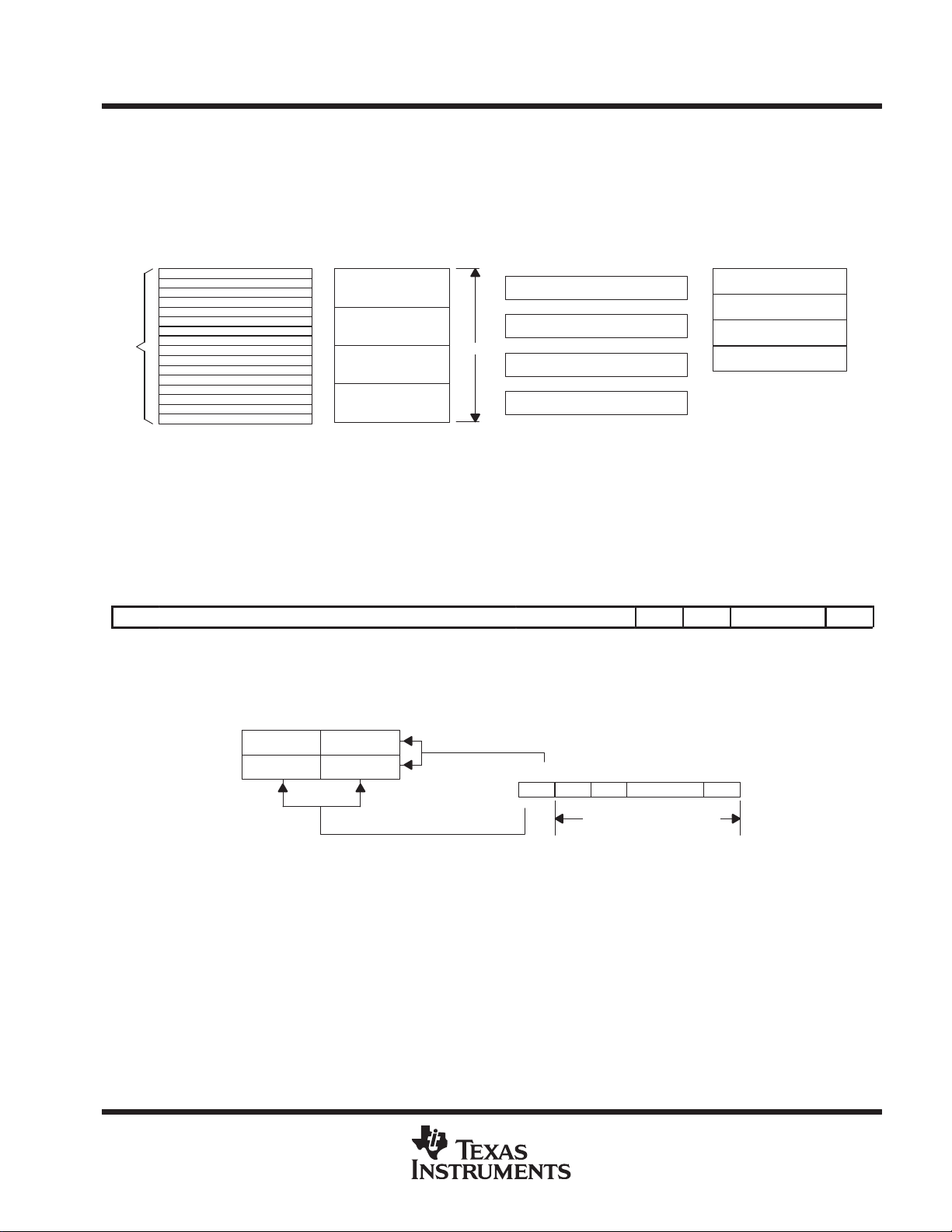
architecture
Figure 1 shows the major components of the ’C80: the master processor (MP), the parallel digital signal
processors (PPs), the transfer controller ( TC), and the IEEE-1149.1 emulation interface. Shared access to
on-chip RAM is achieved through the crossbar. Crossbar connections are represented by
perform three accesses per cycle through its local (L), global (G), and instruction (I) ports. The MP can access
two RAMs per cycle through its crossbar/data (C/D) and instruction (I) ports, and the TC can access one RAM
through its crossbar interface. Up to nine simultaneous accesses are supported in each cycle. Addresses can
be changed every cycle, allowing the crossbar matrix to be changed on a cycle-by-cycle basis. Contention
between processors for the same RAM in the same cycle is resolved by a round-robin priority scheme. In
addition to the crossbar, a 32-bit data path exists between the MP and the TC and VC. This allows the MP to
access TC control registers that are memory-mapped into the MP memory space.
The ’C80 has a 4G-byte address space as shown in Figure 2. The lower 32M bytes are used to address internal
RAM and memory-mapped registers.
. Each PP can
14
POST OFFICE BOX 1443 • HOUSTON, TEXAS 77251–1443
architecture (continued)
POST OFFICE BOX 1443 • HOUSTON, TEXAS 77251–1443
C/D Crossbar/data port
G Global port
L Local port
I Instruction port
Figure 1. Block Diagram Showing Data Paths
Parameter RAM
Data RAM2
Data RAM1
Data RAM0
Instruction Cache
Parameter RAM
Data RAM2
Data RAM1
Data RAM0
Instruction Cache
Parameter RAM
Data RAM2
Data RAM1
Data RAM0
Instruction Cache
Parameter RAM
Data RAM2
Data RAM1
Data RAM0
Instruction Cache
Parameter RAM
Data Cache
Data Cache
Instruction Cache
Instruction Cache
TC
64
64
32
(JTAG)
1149.1
IEEE-
32
32
32
32
32
32 64
32 64
32 64
32 64
LG I
LG I
LG I
LG I
C/D I
OCR
VC
ADSP3
ADSP2
ADSP1
ADSP0
DIGITAL SIGNAL PROCESSOR
MP
SGUS025 – AUGUST 1998
15
SMJ320C80
64
SMJ320C80
DIGITAL SIGNAL PROCESSOR
SGUS025 – AUGUST 1998
architecture (continued)
External Memory
(4064M bytes)
Reserved
(8063K bytes)
Memory-Mapped VC Registers
Memory-Mapped TC Registers
(512 bytes)
(512 bytes)
Reserved
(28K bytes)
MP Instruction Cache
(4K bytes)
Reserved
(28K bytes)
MP Data Cache
(4K bytes)
Reserved
(32K bytes)
ADSP3 Instruction Cache
(2K bytes)
Reserved
(6K bytes)
ADSP2 Instruction Cache
(2K bytes)
Reserved
(6K bytes)
ADSP1 Instruction Cache
(2K bytes)
Reserved
(6K bytes)
ADSP0 Instruction Cache
(2K bytes)
Registers
(8132K bytes)
MP Parameter RAM
(2K bytes)
Registers
(50K bytes)
0xFFFFFFFF
0x02000000
0x01FFFFFF
0x01820400
0x018203FF
0x01820200
0x018201FF
0x01820000
0x0181FFFF
0x01819000
0x01818FFF
0x01818000
0x01817FFF
0x01811000
0x01810FFF
0x01810000
0x0180FFFF
0x01808000
0x01807FFF
0x01807800
0x018077FF
0x01806000
0x01805FFF
0x01805800
0x018057FF
0x01804000
0x01803FFF
0x01803800
0x018037FF
0x01802000
0x01801FFF
0x01801800
0x018017FF
0x01010800
0x010107FF
0x01010000
0x0100FFFF
0x01003800
ADSP3 Parameter RAM
(2K bytes)
Reserved
(2K bytes)
ADSP2 Parameter RAM
(2K bytes)
Reserved
(2K bytes)
ADSP1 Parameter RAM
(2K bytes)
Reserved
(2K bytes)
ADSP0 Parameter RAM
(2K bytes)
Reserved
(16338K bytes)
ADSP3 Data RAM2
(2K bytes)
Reserved
(2K bytes)
ADSP2 Data RAM2
(2K bytes)
Reserved
(2K bytes)
ADSP1 Data RAM2
(2K bytes)
Reserved
(2K bytes)
ADSP0 Data RAM2
(2K bytes)
Reserved
(16K bytes)
ADSP3 Data RAM1
(2K bytes)
ADSP3 Data RAM0
(2K bytes)
ADSP2 Data RAM1
(2K bytes)
ADSP2 Data RAM0
(2K bytes)
ADSP1 Data RAM1
(2K bytes)
ADSP1 Data RAM0
(2K bytes)
ADSP0 Data RAM1
(2K bytes)
ADSP0 Data RAM0
(2K bytes)
0x010037FF
0x01003000
0x01002FFF
0x01002800
0x010027FF
0x01002000
0x01001FFF
0x01001800
0x010017FF
0x01001000
0x01000FFF
0x01000800
0x010007FF
0x01000000
0x00FFFFFF
0x0000B800
0x0000B7FF
0x0000B000
0x0000AFFF
0x0000A800
0x0000A7FF
0x0000A000
0x00009FFF
0x00009800
0x000097FF
0x00009000
0x00008FFF
0x00008800
0x000087FF
0x00008000
0x00007FFF
0x00004000
0x00003FFF
0x00003800
0x000037FF
0x00003000
0x00002FFF
0x00002800
0x000027FF
0x00002000
0x00001FFF
0x00001800
0x000017FF
0x00001000
0x00000FFF
0x00000800
0x000007FF
0x00000000
16
Figure 2. Memory Map
POST OFFICE BOX 1443 • HOUSTON, TEXAS 77251–1443

SMJ320C80
DIGITAL SIGNAL PROCESSOR
SGUS025 – AUGUST 1998
master processor (MP) architecture
The master processor (MP) is a 32-bit RISC processor with an integral IEEE-754 floating-point unit. The MP
is designed for effective execution of C code and is capable of performing at well over 130000 dhrystones/s.
Major tasks which the MP typically performs are:
D
Task control and user interface
D
Information processing and analysis
D
IEEE-754 floating point (including graphics transforms)
MP functional block diagram
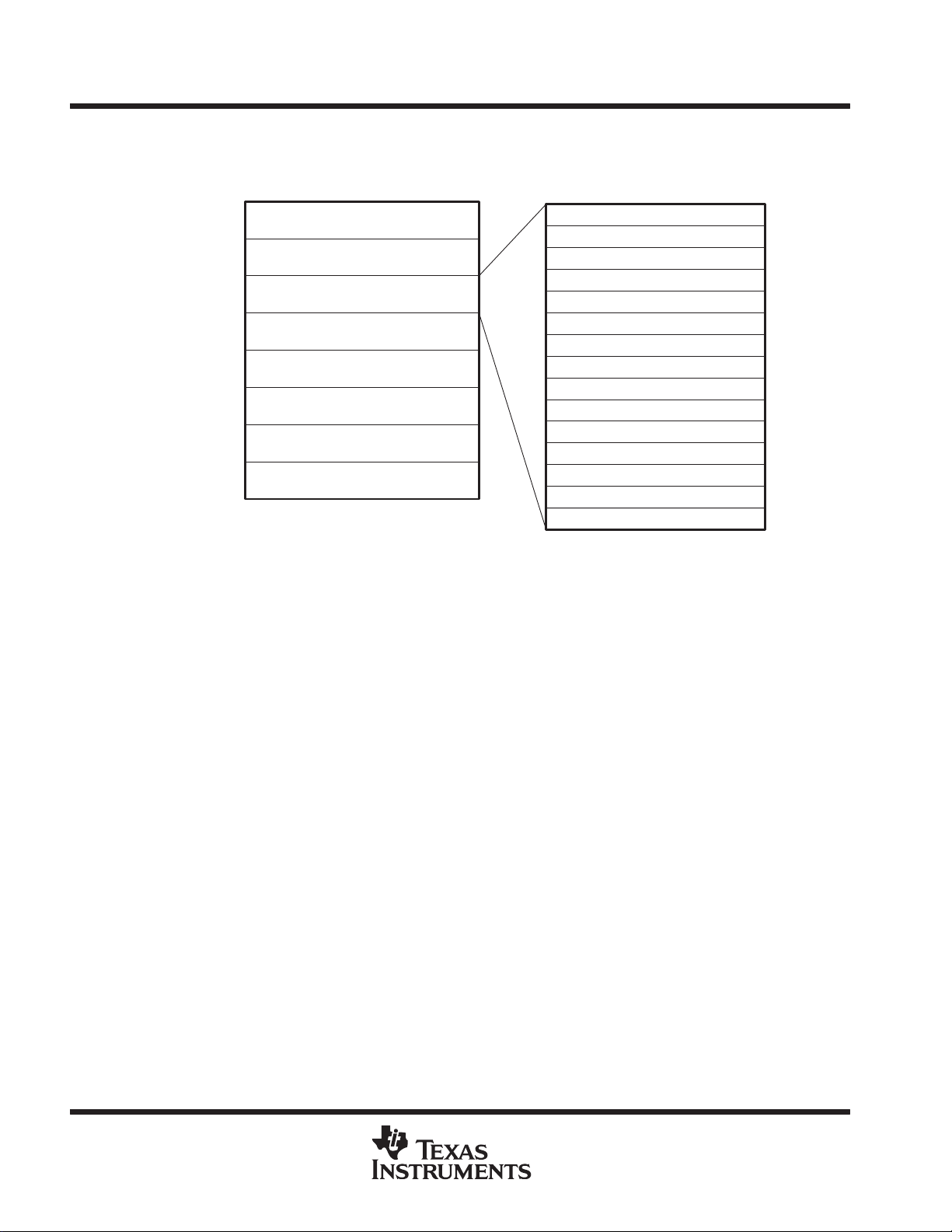
Figure 3 shows a block diagram of the master processor. Key features of the MP include:
D
32-bit RISC processor
– Load/store architecture
– Three operand arithmetic and logical instructions
D
4K-byte instruction cache and 4K-byte data cache
– Four-way set associative
– Least-recently-used (LRU) information replacement
– Data writeback
D
4K-byte noncached parameter RAM
D
Thirty-one 32-bit general-purpose registers
D
Register and accumulator scoreboard
D
15-bit or 32-bit immediate constants
D
32-bit byte addressing
D
Scalable timer
D
Leftmost-one and rightmost-one logic
D
IEEE-754 floating-point hardware
– Four double-precision floating-point vector accumulators
– Vector floating-point instructions
Floating-point operation and parallel load or store
Multiply and accumulate
D
High performance
– 50 million instructions per second (MIPS)
– 100 million floating-point operations per second (MFLOPS)
– Over 130000 dhrystones/s
POST OFFICE BOX 1443 • HOUSTON, TEXAS 77251–1443
17
SMJ320C80
DIGITAL SIGNAL PROCESSOR
SGUS025 – AUGUST 1998
MP functional block diagram (continued)
(Thirty-One 32-Bit Registers)
Register File
Barrel Rotator
Mask Generator
Zero Comparator
Integer Arithmetic and
Logic Unit (ALU)
Leftmost/Rightmost One
Timer
Control Registers
Instruction Register
Program Counters (PCs)
PC Incrementer
Scoreboard
Double-Precision
Floating-Point Multiplier
(Single-Precision Core)
Double-Precision Floating-Point
Accumulators
Double-Precision
Floating-Point Adder
Emulation Logic
Instruction Cache
Controller
Crossbar Interface
Endian Multiplexers
Data-Cache
Controller
Figure 3. MP Block Diagram
MP general-purpose registers
The MP contains 31 32-bit general-purpose registers, R1–R31. Register R0 always reads as zero and writes
to it are discarded. Double-precision values are always stored in an even-odd register pair with the
higher-numbered register always holding the sign bit and exponent. The R0/R1 pair is not available for this use.
A scoreboard keeps track of which registers are awaiting loads or the result of a previous instruction and stalls
the instruction pipeline until the register contains valid data. As a recommended software convention, R1 is
typically used as a stack pointer and R31 as a return-address link register.
Figure 4 shows the MP general-purpose registers.
18
POST OFFICE BOX 1443 • HOUSTON, TEXAS 77251–1443
Not Available
R2, R3
R4, R5
R30, R31
Floating Point
Integer
Unsi
Bit
Integer
SMJ320C80
DIGITAL SIGNAL PROCESSOR
SGUS025 – AUGUST 1998
MP general-purpose registers (continued)
Zero/Discard
R1
R2
R3
R4
R5
•
•
•
R30
R31
32-Bit Registers 64-Bit Register Pairs
Figure 4. MP General-Purpose Registers
The 32-bit registers can contain signed-integer, unsigned-integer, or single-precision floating-point values.
Signed and unsigned bytes and halfwords are sign-extended or zero-filled. Doublewords can be stored in a
64-bit even/odd register pair. Double-precision floating-point values are referenced using the even register
number or the register pair. Figure 5 through Figure 7 show the register data formats.
•
•
•
Single-Precision
Signed 32-bit
gned 32-
S Sign bit
E Exponent
M Value
I Signed integer value
U Unsigned integer value
MS Most significant
LS Least signficant
31 22 0
S E E E E E E E E M M M M M M M M M M M M M M M M M M M M M M M
31 0
S I I I I I I I I I I I I I I I I I I I I I I I I I I I I I I I
MS LS
31 0
U U U U U U U U U U U U U U U U U U U U U U U U U U U U U U U U
MS LS
MS LS
Figure 5. MP Register 32-Bit Data Formats
POST OFFICE BOX 1443 • HOUSTON, TEXAS 77251–1443
19
SMJ320C80
Halfword
DIGITAL SIGNAL PROCESSOR
SGUS025 – AUGUST 1998
MP general-purpose registers (continued)
31 70
Signed Byte
Unsigned Byte
Signed Halfword
S
S S S S S S S S S S S S S S S S S S S S S S S S I I I I I I I
31 70
0
0 0 0 0 0 0 0 0 0 0 0 0 0 0 0 0 0 0 0 0 0 0 0 U U U U U U U U
31 15 0
S
S S S S S S S S S S S S S S S S I I I I I I I I I I I I I I I
MS LS
MS LS
MS LS
Unsigned
S Sign bit(s)
I Signed byte/halfword value
U Unsigned byte/halfword value
MS Most significant
LS Least signficant
31 15 0
0 0 0 0 0 0 0 0 0 0 0 0 0 0 0 0 U U U U U U U U U U U U U U U U
MS LS
Figure 6. MP Register 8-Bit and 16-Bit Data Formats
31 0
Odd Register
MS
31 0
Even Register Least Significant 32-Bit Word
31 19 0
Odd Register
Even Register
S Sign bit(s)
E Exponent
I Signed byte/halfword value
U Unsigned byte/halfword value
MS Most significant
LS Least signficant
S
E E E E E E E E E E E M M M M M M M M M M M M M M M M M M M M
31 0
M
M M M M M M M M M M M M M M M M M M M M M M M M M M M M M M M
Most Significant 32-Bit Word
MS
LS
LS
20
Figure 7. MP Register 64-Bit Data Formats
POST OFFICE BOX 1443 • HOUSTON, TEXAS 77251–1443
SMJ320C80
DIGITAL SIGNAL PROCESSOR
SGUS025 – AUGUST 1998
MP double-precision floating-point accumulators
There are four double-precision floating-point registers (see Figure 8) to accumulate intermediate floating-point
results.
63 0
a0
a1 Accumulator 1
a2 Accumulator 2
a3 Accumulator 3
MSB LSB
S Sign bit
E Exponent
M Value
MS Most significant
LS Least signficant
Figure 8. Double-Precision Floating-Point Accumulators
MP control registers
Accumulator 0
In addition to the general-purpose registers, there are a number of control registers that are used to represent
the state of the processor. Table 1 shows the control register numbers of the accessible registers.
Table 1. Control Register Numbers
NUMBER NAME DESCRIPTION NUMBER NAME DESCRIPTION
0x0000 EPC Exception Program Counter 0x0015–0x001F — Reserved
0x0001 EIP Exception Instruction Pointer 0x0020 SYSSTK System Stack Pointer
0x0002 CONFIG Configuration 0x0021 SYSTMP System Temporary Register
0x0003 — Reserved 0x0022–0x002F — Reserved
0x0004 INTPEN Interrupt Pending Register 0x0030 MPC Emulator Exception Program Counter
0x0005 — Reserved 0x0031 MIP Emulator Exception Instruction Pointer
0x0006 IE Interrupt Enable Register 0x0032 — Reserved
0x0007 — Reserved 0x0033 ECOMCNTL Emulator Communication Control
0x0008 FPST Floating-Point Status 0x0034 ANASTA T Emulation Analysis Status Register
0x0009 — Reserved 0x0035–0x0038 — Reserved
0x000A PPERROR PP Error Register 0x0039 BRK1 Emulation Breakpoint 1 Register
0x000B — Reserved 0x003A BRK2 Emulation Breakpoint 2 Register
0x000C — Reserved 0x003B–0x01FF — Reserved
0x000D PKTREQ
0x000E TCOUNT Current Counter Value 0x0300 iCACHEL Instruction Cache LRU Register
0x000F TSCALE Counter Reload Value 0x0400–0x040F dCACHET Data Cache Tags 0 to 15
0x0010 FLTOP Faulting Operation 0x0500 dCACHEL Data Cache LRU Register
0x0011 FLTADR Faulting Address 0x4000 IN0P Vector Load Pointer 0
0x0012 FLTTAG Faulting Tag 0x4001 IN1P Vector Load Pointer 1
0x0013 FLTDTL Faulting Data (low) 0x4002 OUTP Vector Store Pointer
0x0014 FLTDTH Faulting Data (high)
Packet-Transfer Request
Register
0x0200 – 0x020F iCACHET Instruction Cache Tags 0 to 15
POST OFFICE BOX 1443 • HOUSTON, TEXAS 77251–1443
21
SMJ320C80
DIGITAL SIGNAL PROCESSOR
SGUS025 – AUGUST 1998
MP pipeline registers
The MP uses a three-stage fetch, execute, access (FEA) pipeline. The primary pipeline registers are
manipulated implicitly by branch and trap instructions and are not accessible by the user. The exception and
emulation pipeline registers are user-accessible as control registers. All pipeline registers are 32 bits.
Program Execution Mode
Normal Exception Emulation
Program Counter PC EPC MPC
Instruction Pointer IP EIP MIP
Instruction Register IR
• Instruction register (IR) contains the instruction being
executed.
• Instruction pointer (IP) points to the instruction being
executed.
• Program counter (PC) points to the instruction being
fetched.
• Exception/emulator instruction pointer (EIP/MIP) points to the
instruction that would have been executed had the exception /
emulation trap not occurred.
• Exception/emulator program counter (EPC/MPC) points to the
instruction to be fetched on returning from the exception/emulation
trap.
Figure 9. MP FEA Pipeline Registers
configuration (CONFIG) register (0x0002)
The CONFIG register controls or reflects the state of certain options as shown in Figure 10.
3130292827262524232221201918171615141312111
E
RTHX Reserved Type Reserved Release Reserved
Endian mode; 0 = big-endian, 1 = little-endian, read only
E
PPData RAM round robin; 0 = fixed, 1 = variable, read/write
R
TC packet transfer (PT) round robin; 0 = variable, 1 = fixed, read/write
T
High priority MP events; 0 = disabled, 1 = enabled, read/write
H
Externally initiated packet transfers; 0 = disabled, 1 = enabled, read/write
X
Number of PPs in device, read only
Type
Release
SMJ320C80 version number
9876543210
0
Figure 10. CONFIG Register
22
POST OFFICE BOX 1443 • HOUSTON, TEXAS 77251–1443
SMJ320C80
DIGITAL SIGNAL PROCESSOR
SGUS025 – AUGUST 1998
interrupt-enable (IE) register (0x0006)
The IE register contains enable bits for each of the interrupts/traps as shown in Figure 11. The
global-interrupt-enable (ie) bit and the appropriate individual interrupt-enable bit must be set in order for an
interrupt to occur.
3130292827262524232221201918171615141312111
p
x4x3bppbpcm
e
PP error
pe
External interrupt 4 (LINT4
x4
x3
External interrupt 3 (EINT3
bp
Bad packet transfer
pb
Packet transfer busy
pc
Packet transfer complete
mi
MP message interrupt
p3
PP3 message interrupt
i
)
)
p3p2p1p0iomfx2x
PP2 message interrupt
p2
PP1 message interrupt
p1
PP0 message interrupt
p0
Integer overflow
io
Memory fault
mf
External interrupt 2 (EINT2
x2
x1
External interrupt 1 (EINT1
ti
MP timer interrupt
1
9876543210
0
f1f0fxfuf
ti
Frame-timer 1 interrupt
f1
Frame-timer 0 interrupt
f0
Floating-point inexact
fx
Floating-point underflow
fu
Floating-point overflow
fo
Floating-point divide-by-zero
)
)
fz
Floating-point invalid
fi
Global-interrupt enable
ie
o
fz fi ie
Figure 11. IE Register
interrupt-pending (INTPEN) register (0x0004)
The bits in INTPEN register show the current state of each interrupt/trap. Pending interrupts do not occur unless
the ie bit and corresponding interrupt-enable bit are set. Software must write a 1 to the appropriate INTPEN bit
to clear an interrupt. Figure 12 shows the INTPEN register locations.
3130292827262524232221201918171615141312111
p
x4x3bppbpcm
e
PP error
pe
External interrupt 4 (LINT4
x4
x3
External interrupt 3 (EINT3
bp
Bad packet transfer
pb
Packet transfer busy
pc
Packet transfer complete
mi
MP message interrupt
p3
PP3 message interrupt
i
)
)
p3p2p1p0iomfx2x
PP2 message interrupt
p2
PP1 message interrupt
p1
PP0 message interrupt
p0
Integer overflow
io
Memory fault
mf
External interrupt 2 (EINT2
x2
x1
External interrupt 1 (EINT1
ti
MP timer interrupt
1
9876543210
0
f1f0fxfuf
ti
Frame-timer 1 interrupt
f1
Frame-timer 0 interrupt
f0
Floating-point inexact
fx
Floating-point underflow
fu
Floating-point overflow
fo
Floating-point divide-by-zero
)
)
fz
Floating-point invalid
fi
Global-interrupt enable
ie
fz fi
o
Figure 12. INTPEN Register
POST OFFICE BOX 1443 • HOUSTON, TEXAS 77251–1443
23
SMJ320C80
DIGITAL SIGNAL PROCESSOR
SGUS025 – AUGUST 1998
floating-point status (FPST) register (0x0008)
FPST contains status and control information for the floating-point unit (FPU) as shown in Figure 13. Bits 17–21
are read/write FPU control bits. Bits 22–26 are read/write accumulated status bits. All other bits show the status
of the last FPU instruction to complete and are read only.
3130292827262524232221201918171615141312111
dest
dest
az
ao
au
ax
sm
vm
drm
opcode
e1
azaoauaxsmfsv
ai
Destination register value
Accumulated value invalid
ai
Accumulated divide-by-zero
Accumulated overflow
Accumulated underflow
Accumulated inexact
Sequential mode select
Floating-point stall
fs
Vector fast mode
Rounding mode
Last opcode
The tenth MSB of exponent
00 – nearest 10 – positive ∞
01 – zero 11 – negative ∞
drm opcode
m
e1e
0
The ninth MSB of exponent
e0
Destination precision
pd
Rounding mode
rm
Int multiply overflow
mo
Invalid
i
Divide-by-zero
z
Overflow
o
Underflow
u
Inexact
x
9876543210
0
pd rm mo i z o u x
00 – single float 10 – signed int
01 – double float 11 – unsigned int
00 – nearest 10 – positive ∞
01 – zero 11 – negative ∞
Figure 13. FPST Register
PP error (PPERROR) register (0x000A)
The bits in the PPERROR register reflect parallel processor errors (see Figure 14). The MP can use these when
a PP error interrupt occurs to determine the cause of the error.
3130292827262524232221201918171615141312111
Reserved
h PPhalted
I PP illegal instruction
f PP fault type
0 icache
1 Direct external access (DEA)
h h h h Reserved i i i i Reserved f f f f
PP# 3 2 1 0 PP# 3 2 1 0 PP# 3 2 1 0
9876543210
0
Figure 14. PPERROR Register
packet-transfer request (PKTREQ) register (0x000D)
PKTREQ controls the submission and priority of packet-transfer requests as shown in Figure 15. It also
indicates that a packet transfer is currently active.
3130292827262524232221201918171615141312111
Reserved
I Immediate (urgent) priority selected
F High (foreground) priority selected
S Suspend packet transfer
Q Packet transfer queued; read only
P Submit packet-transfer request
9876543210
0
I F S Q P
Figure 15. PKTREQ Register
24
POST OFFICE BOX 1443 • HOUSTON, TEXAS 77251–1443
SMJ320C80
DIGITAL SIGNAL PROCESSOR
SGUS025 – AUGUST 1998
memory-fault registers
The five read-only memory-fault registers contain information about memory address exceptions, as shown in
Figure 16.
FLTOP
(0x0010)
FLTTAG
(0x0011)
FLTADR
(0x0012)
FLTDTH
(0x0013)
FLTDTL
(0x0014)
3130292827262524232221201918171615141312111
Dest
3130292827262524232221201918171615141312111
31 0
Dest
Destination Register Number
K
Kind of Operation:
00 – load
01 – unsigned load
10 – store
11 – cache flush/clean
Size of Data:
SZ
00 – 8-bit
01 – 16-bit
10 – 32-bit
11 – 64-bit
Reserved K SZ i d x r Reserved Block
22-Bit Cache Tag Address
Faulting Address Accessed by the Instruction
Faulting Write Most-Significant-Data Word
Faulting Write Least-Significant-Data Word
MP icache fault
i
MP dcache fault
d
DEA Fault
x
Modified return sequence
r
Block
Faulting block number
Sub-block is present.
P
Dirty bit set
D
9876543210
0
9876543210
0
P D P D P D P D
3 2 1 0
Sub-Block
Figure 16. Memory-Fault Registers
POST OFFICE BOX 1443 • HOUSTON, TEXAS 77251–1443
25
SMJ320C80
DIGITAL SIGNAL PROCESSOR
SGUS025 – AUGUST 1998
MP cache registers
The ILRU and DLRU registers track least-recently-used (LRU) information for the sixteen instruction-cache and
sixteen data-cache blocks. The ITAGxx registers contain block addresses and the present flags for each
sub-block. DT AGxx registers are identical to IT AGxx registers but include dirty bits for each sub-block. Figure 17
shows the cache registers.
ILRU (0x0300)
DLRU (0x0500)
3130292827262524232221201918171615141312111
MRU
NMRU NLRU LRU MRU NMRU NLRU LRU MRU NMRU NLRU LRU MRU NMRU NLRU LRU
Set 3
3130292827262524232221201918171615141312111
22-Bit Cache Tag Address
Set 2 Set 1 Set 0
ITAG0–ITAG15 (0x0200–0x020F)
9876543210
0
9876543210
0
P P P P
3 2 1 0
Sub-Block
DTAG0–DTAG15 (0x0400–0x040F)
3130292827262524232221201918171615141312111
22-Bit Cache Tag Address
MRU
NMRU
NLRU
mru, nmru, nlru, and lru have the value 0, 1, 2, or 3 representing the block number and are mutually exclusive for each set.
Most-recently-used
Next most-recently-used
Next least-recently-used
LRU
Least-recently-used
P
Sub-block present
D
Sub-block dirty
9876543210
0
P D P D P D P D
3 2 1 0
Sub-Block
Figure 17. Cache Registers
26
POST OFFICE BOX 1443 • HOUSTON, TEXAS 77251–1443
SMJ320C80
DIGITAL SIGNAL PROCESSOR
SGUS025 – AUGUST 1998
MP cache architecture
The MP contains two four-way set-associative, 4K caches for instructions and data. Each cache is divided into
four sets with four blocks in each set. Each block represents 256 bytes of contiguous instructions or data and
is aligned to a 256-byte address boundary. Each block is partitioned into four sub-blocks that each contain
sixteen 32-bit words and are aligned to 64-byte boundaries within the block. Cache misses cause one sub-block
to be loaded into cache. Figure 18 shows the cache architecture for one of the four sets in each cache. Figure 19
shows how addresses map into the cache using the cache tags and address bits.
LRU in SET 0
NLRU in SET 0
NMRU in SET 0
MRU in SET 0
LRU Stack for SET 0
Sub-Blocks
LRU Least-recently-used
NLRU Next least-recently-used
NMRU Next most-recently-used
MRU Most-recently-used
Block 0
Block 1
Block 2
Block 3
Tag Reg 0 (Block 0)
Tag Reg 1 (Block 1)
Set 0
Tag Reg 2 (Block 2)
Tag Reg 3 (Block 3)
Figure 18. MP Cache Architecture (x4 Sets)
32-Bit Logical Address
3130292827262524232221201918171615141312111
TTTTTTTTTTTTTTTTTTTTTSSssWWWWBB
T
On-Chip MP 4K Cache RAMS
Bank 0
Bank 1
9876543210
0
Set 0
Set 1 Set 3
T – Tag Address Bits s – Sub-Block (within block) Select (0–3) B – Byte (within word) Select (0 – 3)
S – Set Select Bits (0–3) W – Word (within sub-block) Select (0–15) A – Block Select (which tag matched) (0 –3)
Set 2
11109876
SSAAss
Address in On-Chip
Cache Bank
543210
WWWWB B
Figure 19. MP Cache Addressing
POST OFFICE BOX 1443 • HOUSTON, TEXAS 77251–1443
27
SMJ320C80
DIGITAL SIGNAL PROCESSOR
SGUS025 – AUGUST 1998
MP parameter RAM
The parameter RAM is a noncachable, 2K-byte, on-chip RAM that contains MP interrupt vectors, MP-requested
TC task buffers, and a general-purpose area. Figure 20 shows the parameter RAM address map.
0x001010000–0x0101007F
0x001010800–0x010100DF
0x0010100E0–0x010100FB
0x0010100FC–0x010100FF
0x001010100–0x0101017F
0x001010180–0x0101021F
0x001010220–0x0101029F
0x0010102A0–0x010107FF
Suspended PT Parameters
(128 Bytes)
Reserved
(64 Bytes)
XPT Linked List Start Addresses
(60 Bytes)
MP Linked List Start Address
Off-Chip to Off-Chip PT Buffer
(128 Bytes)
Interrupt and Trap Vectors
(160 Bytes)
XPT Off-Chip to Off-Chip PT Buffer
(128 Bytes)
General-Purpose RAM
(3472 Bytes)
Figure 20. MP Parameter RAM
XPTf Linked List Start Add.
XPTe Linked List Start Add.
XPTd Linked List Start Add.
XPTc Linked List Start Add.
XPTb Linked List Start Add.
XPTa Linked List Start Add.
XPT9 Linked List Start Add.
XPT8 Linked List Start Add.
XPT7 Linked List Start Add. 0x010100E0
XPT6 Linked List Start Add. 0x010100E4
XPT5 Linked List Start Add. 0x010100E8
XPT4 Linked List Start Add. 0x010100EC
XPT3 Linked List Start Add. 0x010100F0
XPT2 Linked List Start Add. 0x010100F4
XPT1 Linked List Start Add. 0x010100F8
28
POST OFFICE BOX 1443 • HOUSTON, TEXAS 77251–1443
MP interrupt vectors
Table 2 and Table 3 show the MP interrupts and traps and their vector addresses.
Table 2. Maskable Interrupts
SMJ320C80
DIGITAL SIGNAL PROCESSOR
SGUS025 – AUGUST 1998
IE BIT
(TRAP#)
0 ie 0x01010180
2 fi 0x01010188 Floating-point invalid
3 fz 0x0101018C Floating-point divide-by-zero
5 fo 0x01010194 Floating-point overflow
6 fu 0x01010198 Floating-point underflow
7 fx 0x0101019C Floating-point inexact
8 f0 0x010101A0 Reserved
9 f1 0x010101A4 Reserved
10 ti 0x010101A8 MP timer interrupt
11 x1 0x010101AC External interrupt 1 (EINT1)
12 x2 0x010101B0 External interrupt 2 (EINT2)
14 mf 0x010101B8 Memory fault
15 io 0x010101BC Integer overflow
16 p0 0x010101C0 PP0 message interrupt
17 p1 0x010101C4 PP1 message interrupt
18 p2 0x010101C8 Reserved
19 p3 0x010101CC Reserved
25 mi 0x010101E4 MP message interrupt
26 pc 0x010101E8 Packet-transfer complete
27 pb 0x010101EC Packet-transfer busy
28 bp 0x010101F0 Bad packet transfer
29 x3 0x010101F4 External interrupt 3 (EINT3)
30 x4 0x010101F8 External interrupt 4 (LINT4)
31 pe 0x010101FC PP error
NAME
VECTOR
ADDRESS
MASKABLE INTERRUPT
Table 3. Nonmaskable Traps
TRAP
NUMBER
32 e1 0x01010200 Emulator trap1 (reserved)
33 e2 0x01010204 Emulator trap2 (reserved)
34 e3 0x01010208 Emulator trap3 (reserved)
35 e4 0x0101020C Emulator trap4 (reserved)
36 fe 0x01010210 Floating-point error
37 0x01010214 Reserved
38 er 0x01010218 Illegal MP instruction
39 0x0101021C Reserved
72
to
415
NAME
POST OFFICE BOX 1443 • HOUSTON, TEXAS 77251–1443
VECTOR
ADDRESS
0x010102A0 to
0x010107FC
NONMASKABLE TRAP
System- or user-defined
29
SMJ320C80
DIGITAL SIGNAL PROCESSOR
SGUS025 – AUGUST 1998
MP opcode formats
The three basic classes of MP instruction opcodes are: short immediate, three register, and long immediate.
Figure 21 shows the opcode structure for each class of instruction.
31 27 26 22 21 15 14 0
Short
Immediate
Three
Register
Long
Immediate
Dest
31 27 26 22 21 20 19 13 12 11 5 4 0
Dest
31 27 26 22 21 20 19 13 12 11 5 4 0
Dest
Source 2 Opcode 15-Bit Immediate
Source 2 1 1 Opcode 0 Options Source 1
Source 2 1 1 Opcode 1 Options Source 1
32-Bit Long Immediate
Figure 21. MP Opcode Formats
MP opcode summary
Table 4 through Table 6 show the opcode formats for the MP. Table 7 summarizes the master processor
instruction set.
30
POST OFFICE BOX 1443 • HOUSTON, TEXAS 77251–1443

MP opcode summary (continued)
SMJ320C80
DIGITAL SIGNAL PROCESSOR
SGUS025 – AUGUST 1998
Table 4. Short-Immediate Opcodes
313029282726252423222120191817161514131211100908070605040302010
illop0 Dest Source 0 0 0 0 0 0 0 Unsigned Immediate
trap – – – – E – – – – – 0 0 0 0 0 0 1 Unsigned Trap Number
cmnd – – – – – – – – – – 0 0 0 0 0 1 0 Unsigned Immediate
rdcr Dest – – – – – 0 0 0 0 1 0 0 Unsigned Control Register Number
swcr Dest Source 0 000101 Unsigned Control Register Number
brcr – – – – – – – – – – 0 0 0 0 1 1 0 Unsigned Control Register Number
shift.dz Dest Source 0 0 0 1 0 0 0 – – – i n Endmask Rotate
shift.dm Dest Source 0 001001–––i n Endmask Rotate
shift.ds Dest Source 0 001010–––i n Endmask Rotate
shift.ez Dest Source 0 001011–––i n Endmask Rotate
shift.em Dest Source 0 001100–––i n Endmask Rotate
shift.es Dest Source 0 001101–––i n Endmask Rotate
shift.iz Dest Source 0 001110–––i n Endmask Rotate
shift.im Dest Source 0 001111–––i n Endmask Rotate
and.tt Dest Source2 0 0 1 0 0 0 1 Unsigned Immediate
and.tf Dest Source2 0 010010 Unsigned Immediate
and.ft Dest Source2 0 010100 Unsigned Immediate
xor Dest Source2 0 010110 Unsigned Immediate
or.tt Dest Source2 0 010111 Unsigned Immediate
and.ff Dest Source2 0 011000 Unsigned Immediate
xnor Dest Source2 0 011001 Unsigned Immediate
or.tf Dest Source2 0 011011 Unsigned Immediate
or.ft Dest Source2 0 011101 Unsigned Immediate
or.f f Dest Source2 0 011110 Unsigned Immediate
ld Dest Base 0 1 0 0 M SZ Signed Offset
ld.u Dest Base 0 101M SZ Signed Offset
st Source Base 0 110M SZ Signed Offset
dcache – – – – F Source2 0 1 1 1 M 0 0 Signed Offset
bsr Link – – – – – 1 0 0 0 0 0 A Signed Offset
jsr Link Base 1 00010A Signed Offset
bbz BITNUM Source 1 0 0 1 0 0 A Signed Offset
bbo BITNUM Source 1 00101A Signed Offset
bcnd Cond Source 1 00110A Signed Offset
cmp Dest Source2 1 0 1 1 0 0 0 Signed Immediate
add Dest Source2 1 0 1 1 0 0 U Signed Immediate
sub Dest Source2 1 01101U Signed Immediate
– Reserved bit (code as 0) M Modify, write modified address back to register
A Annul delay slot instruction if branch taken n Rotate sense for shifting
E Emulation trap bit SZ Size (0 = byte, 1 = halfword, 2 = word, 3 = doubleword)
F Clear present flags U Unsigned form
i Invert endmask
0
POST OFFICE BOX 1443 • HOUSTON, TEXAS 77251–1443
31

SMJ320C80
DIGITAL SIGNAL PROCESSOR
SGUS025 – AUGUST 1998
MP opcode summary (continued)
Table 5. Long-Immediate and Three-Register Opcodes
313029282726252423222120191817161514131211100908070605040302010
trap – – – – E – – – – – 1 1 0 0 0 0 0 0 1 I – – – – – – – IND TR
cmnd – – – – – – – – – – 1 1 0 0 0 0 0 1 0 I – – – – – – – Source1
rdcr Dest – – – – – 1 1 0 0 0 0 1 0 0 I – – – – – – – IND CR
swcr Dest Source 1 10000101I–– – – – – – IND CR
brcr – – – – – – – – – – 1 1 0 0 0 0 1 1 0 I – – – – – – – IND CR
shift.dz Dest Source 1 1 0 0 0 1 0 0 0 I i n Endmask Rotate
shift.dm Dest Source 1 10001001I in Endmask Rotate
shift.ds Dest Source 1 10001010I in Endmask Rotate
shift.ez Dest Source 1 10001011I in Endmask Rotate
shift.em Dest Source 1 10001100I in Endmask Rotate
shift.es Dest Source 1 10001101I in Endmask Rotate
shift.iz Dest Source 1 10001110I in Endmask Rotate
shift.im Dest Source 1 10001111I in Endmask Rotate
and.tt Dest Source2 1 1 0 0 1 0 0 0 1 I – – – – – – – Source1
and.tf Dest Source2 1 10010010I–– – – – – – Source1
and.ft Dest Source2 1 10010100I–– – – – – – Source1
xor Dest Source2 1 10010110I–– – – – – – Source1
or.tt Dest Source2 1 10010111I–– – – – – – Source1
and.ff Dest Source2 1 10011000I–– – – – – – Source1
xnor Dest Source2 1 10011001I–– – – – – – Source1
or.tf Dest Source2 1 10011011I–– – – – – – Source1
or.ft Dest Source2 1 10011101I–– – – – – – Source1
or.ff Dest Source2 1 10011110I–– – – – – – Source1
ld Dest Base 1 1 0 1 0 0 M SZ I S D – – – – – Offset
ld.u Dest Base 1 10101M SZ I S D – – – – – Offset
st Source Base 1 10110M SZ I S D – – – – – Offset
dcache – – – – F Source2 1 1 0 1 1 1 M 0 0 I 0 0 – – – – – Source
bsr Link – – – – – 1 1 1 0 0 0 0 0 A I – – – – – – – Offset
jsr Link Base 1 1100010AI–– – – – – – Offset
bbz BITNUM Source 1 1 1 0 0 1 0 0 A I – – – – – – – Target
bbo BITNUM Source 1 1100101AI–– – – – – – Target
bcnd Cond Source 1 1100110AI–– – – – – – Target
cmp Dest Source2 1 1 1 0 1 0 0 0 0 I – – – – – – – Source1
add Dest Source2 1 1 1 0 1 1 0 0 U I – – – – – – – Source1
sub Dest Source2 1 1101101UI–– – – – – – Source1
0
– Reserved bit (code as 0) l Long immediate
D Direct external access bit M Modify, write modified address back to register
E Emulation trap bit n Rotate sense for shifting
F Clear present flags S Scale offset by data size
i Invert endmask SZ Size (0 = byte, 1 = halfword, 2 = word, 3 = doubleword
32
POST OFFICE BOX 1443 • HOUSTON, TEXAS 77251–1443

MP opcode summary (continued)
Table 6. Miscellaneous Instruction Opcodes
SMJ320C80
DIGITAL SIGNAL PROCESSOR
SGUS025 – AUGUST 1998
313029282726252423222120191817161514131211100908070605040302010
vadd Mem Src/Dst Source2/Dest 1 1 1 1 0 – 0 0 0 I – m P – d m s Source1
vsub Mem Src/Dst Source2/Dest 1 1110–001I–mP–dms Source1
vmpy Mem Src/Dst Source2/Dest 1 1110–010I–mP–dms Source1
vmsub Mem Src/Dst Dest 1 1110a011IamPZ–m– Source1
vrnd(F P) Mem Src/Dst Dest 1 1110a100IamP PD m s Source1
vrnd(Int) Mem Src/Dst Dest 1 1110–101I–mP–dms Source1
vmac Mem Src/Dst Source2 1 1 1 1 0 a 1 1 0 I a m P Z – m – Source1
vmac Mem Src/Dst Source2 1 1110a111IamPZ–m– Source1
fadd Dest Source2 1 1 1 1 1 0 0 0 0 I – PD P2 P1 Source1
fsub Dest Source2 1 11110001I– PD P2 P1 Source1
fmpy Dest Source2 1 11110010I– PD P2 P1 Source1
fdiv Dest Source2 1 11110011I– PD P2 P1 Source1
frndx Dest – ––––111110100I– PD RM P1 Source1
fcmp Dest Source2 1 11110101I– – P2 P1 Source1
fsqrt Dest – ––––111110111I– PD – –P1 Source1
lmo Dest Source 1 1 1 1 1 1 0 0 0 – – – – – – – – – – – – –
rmo Dest Source 1 11111001–––––––––––––
estop – – – – – – – – – – 1 1 1 1 1 1 1 1 0 – – – – – – – – – – – – –
illopF – –––––––––111111111C––––––––––––
– Reserved bit (code as 0) P Destination precision for parallel load/store (0 = single, 1 = double)
a Floating-point accumulator select P1 Precision of source1 operand
C Constant operands rather than register P2 Precision of source2 operand
d Destination precision for vector (0 = sp, 1 = dp) PD Precision of destination result
l Long immediate 32-bit data RM Rounding Mode (0 = N, 1 = Z, 2 = P, 3 = M)
m Parallel memory operation specifier S Scale offset by data size
Mem Src/Dst Vector store or load source/dst register Z Use 0 rather than accumulator
Dest Destination register
0
POST OFFICE BOX 1443 • HOUSTON, TEXAS 77251–1443
33

SMJ320C80
DIGITAL SIGNAL PROCESSOR
SGUS025 – AUGUST 1998
MP opcode summary (continued)
Table 7. Summary of MP Opcodes
INSTRUCTION DESCRIPTION INSTRUCTION DESCRIPTION
add Signed integer add or.ff Bitwise OR with 1s complement
and.tt Bitwise AND or.ft Bitwise OR with 1s complement
and.ff Bitwise AND with 1s complement or.tf Bitwise OR with 1s complement
and.ft Bitwise AND with 1s complement rdcr Read control register
and.tf Bitwise AND with 1s complement rmo Rightmost one
bbo Branch bit one shift.dz Shift, disable mask, zero extend
bbz Branch bit zero shift.dm Shift, disable mask, merge
bcnd Branch conditional shift.ds Shift, disable mask, sign extend
br Branch always shift.ez Shift, enable mask, zero extend
brcr Branch control register shift.em Shift, enable mask, merge
bsr Branch and save return shift.es Shift, enable mask, sign extend
cmnd Send command shift.iz Shift, invert mask, zero extend
cmp Integer compare shift.im Shift, invert mask, merge
dcache Flush data cache sub-block st Store register into memory
estop Emulation stop sub Signed integer subtract
fadd Floating-point add swcr Swap control register
fcmp Floating-point compare trap T rap
fdiv Floating-point divide vadd Vector floating-point add
fmpy Floating-point multiply vmac
frndx Floating-point convert/round vmpy V ector floating-point multiply
fsqrt Floating-point square root vmsc
fsub Floating-point subtract vmsub
illop Illegal operation vrnd(FP) Vector round with floating-point input
jsr Jump and save return vrnd(Int) Vector round with integer input
ld Load signed into register vsub Vector floating-point subtract
ld.u Load unsigned into register xnor Bitwise exclusive NOR
lmo Leftmost one xor Bitwise exclusive OR
or.tt Bitwise OR
Vector floating-point multiply and add to
accumulator
Vector floating-point multiply and subtract
from accumulator
Vector floating-point subtract accumulator
from source
34
POST OFFICE BOX 1443 • HOUSTON, TEXAS 77251–1443

SMJ320C80
DIGITAL SIGNAL PROCESSOR
SGUS025 – AUGUST 1998
PP architecture
The parallel processor (PP) is a 32-bit integer DSP optimized for imaging and graphics applications. Each PP
can execute in parallel: a multiply, ALU operation, and two memory accesses within a single instruction. This
internal parallelism allows a single PP to achieve over 500 million operations per second for certain algorithms.
The PP has a three-input ALU that supports all 256 three input Boolean combinations and many combinations
of arithmetic and Boolean functions. Data-merging and bit-to-byte, bit-to-word, and bit-to-halfword translations
are supported by hardware in the input data path to the ALU. Typical tasks performed by a PP include:
D
Pixel-intensive processing
– Motion estimation
– Convolution
– PixBLTs
– Warp
– Histogram
– Mean square error
D
Domain transforms
– Discrete Cosine Transform (DCT)
– Fast Fourier Transform (FFT)
– Hough
D
Core graphics functions
– Line
– Circle
– Shaded fills
– Fonts
D
Image analysis
– Segmentation
– Feature extraction
D
Bit-stream encoding/decoding
– Data merging
– Table look-ups
POST OFFICE BOX 1443 • HOUSTON, TEXAS 77251–1443
35

SMJ320C80
DIGITAL SIGNAL PROCESSOR
SGUS025 – AUGUST 1998
PP functional block diagram
Figure 22 shows a block diagram of a parallel processor. Key features of the PP include:
D
64-bit instruction word (supports multiple parallel operations)
D
Three-stage pipeline for fast instruction cycle
D
Numerous registers
– 8 data, 10 address, 6 index registers
– 20 other user-visible registers
D
Data Unit
– 16 x 16 integer multiplier (optional dual 8 x 8)
– Splittable 3-input ALU
– 32-bit barrel rotator
– Mask generator
– Multiple status flag expander for translations to/from 1 bit-per-pixel space.
– Conditional assignment of data unit results
– Conditional source selection
– Special processing hardware
Leftmost one/rightmost one
Leftmost bit change/rightmost bit change
D
Memory addressing
– Two address units (global and local) provide up to two 32-bit accesses in parallel with data unit
operation.
– 12 addressing modes (immediate and indexed)
– Byte, halfword, and word addressability
– Scaled indexed addressing
– Conditional assignment for loads
– Conditional source selection for stores
D
Program flow
– Three hardware loop controllers
Zero overhead looping/branching
Nested loops
Multiple loop endpoints
– Instruction cache management
– PC mapped to register file
36
– Interrupts for messages and context switching
D
Algebraic assembly language
POST OFFICE BOX 1443 • HOUSTON, TEXAS 77251–1443

PP functional block diagram (continued)
SMJ320C80
DIGITAL SIGNAL PROCESSOR
SGUS025 – AUGUST 1998
Data Unit
Local Destination/Source
Global Source
Global Destination
d0–d7
mf and sr
Registers
Local Address Unit Global Address Unit
a0–a4, a7
Local Data Path Global Data Path
x0–x2
Multiplier
Data Path
sp = a6 = a14
Program Flow Control Unit
ALU Data Path
Expander
Mask Generator
Barrel Rotator
Three-Input ALU
a8–a12,
a15
x8–x10
Repl
Local
Data Port
A/S
Repl
Global
Data Port
Three Zero-Overhead
Loop/Branch Controllers
A/S
Repl Replicate hardware
A/S Align/sign-extend hardware
Figure 22. PP Block Diagram
POST OFFICE BOX 1443 • HOUSTON, TEXAS 77251–1443
Instruction and Cache Control
64 32
Instruction
Port
IAP Instruction address port
LAP Local address port
GAP Global address port
32
IAP LAP GAP
37

SMJ320C80
DIGITAL SIGNAL PROCESSOR
SGUS025 – AUGUST 1998
PP registers
The PP contains many general-purpose registers, status registers, and configuration registers. All PP registers
are 32-bit registers. Figure 23 shows the accessible registers of the PP blocks.
Data-Unit Registers
Data Registers
Multiple Flags
Status
Address-Unit Registers
Address Registers
a8
a9
a10
a11
a12
a14/sp
a15 = 0
d0/EALU Operation
d1
d2
d3
d4
d5
d6
d7
Global-Address Unit Local-Address Unit
Index Flags
x8
x9
x10
Stack Pointer
Same Physical
Register
mf
Address Registers
sr
a0
a1
a2
a3
a4
a6/sp
a7 = 0
Index Flags
x0
x1
x2
Prgram Flow Control (PFC) Unit Registers
PC-Related Registers
pc (br, call)
iprs
ipa (read only)
ipe (read only)
Cache Tags
tag0 (read only)
tag1 (read only)
tag2 (read only)
tag3 (read only)
38
Loop Addresses
ls0
ls1
ls2
le0
le1
le2
Loop Control
lctl
Loop Counts
lr0
lr1
lr2
lc0
lc1
lc2
Figure 23. PP Registers
POST OFFICE BOX 1443 • HOUSTON, TEXAS 77251–1443
Communications
comm
Interrupts
lntflg
inten

SMJ320C80
DIGITAL SIGNAL PROCESSOR
SGUS025 – AUGUST 1998
PP data-unit registers
The data unit contains eight 32-bit general-purpose data registers (d0–d7) referred to as the D registers. The
d0 register also acts as the control register for extended ALU (EALU) operations.
d0 register
Figure 24 shows the format when d0 is used as the EALU control register.
31 30 29 28 27 26 25 24 23 22 21 20 19 18 17 16 15 14 13 12 11 10 9 8 7 6 5 4 3 2 1 0
FMOD A EALU Function Code C I S N E F T – – DMS M R U DBR
FMOD
Function modifiers
A
Arithmetic enable
C
EALU carry-In
I
Invert-carry-In
S
Sign extend
N
Nonmultiple mask
DMS
DBR
E
Explicit multiple carry-in
F
Expanded multiple flags
Default multiply shift amount
M
Split multiply
R
Rounded multiply
Default barrel rotate amount
Figure 24. d0 Format for EALU Operations
multiple flags (mf) register
The mf register records status information from each split ALU segment for multiple arithmetic operations. The
mf register can be expanded to generate a mask for the ALU. Figure 25 shows the mf register format.
31 30 29 28 27 26 25 24 23 22 21 20 19 18 17 16 15 14 13 12 11 10 9 8 7 6 5 4 3 2 1 0
Figure 25. mf Register Format
status register (sr)
The sr contains status and control bits for the PP ALU. See Figure 26.
31 30 29 28 27 26 25 24 23 22 21 20 19 18 17 16 15 14 13 12 11 10 9 8 7 6 5 4 3 2 1 0
N C V Z – – – – – – – – – – – – – – – – – – – MSS R Msize Asize
N
Negative status bit
C
Carry status bit
V
Overflow status bit
Z
Zero status bit
R
Rotation bit
MSS
Msize
Asize
mf status selection
00 – set by zero 10 – set by extended result
01 – set by sign 11 – reserved
Expander data size
Split ALU data size
Figure 26. sr Format
PP address-unit registers
address registers
The address unit contains ten 32-bit address registers which contain the base address for address
computations or which can be used for general-purpose data. The registers a0 – a4 are used for local-address
computations and registers a8–a12 are used for global-address computations.
POST OFFICE BOX 1443 • HOUSTON, TEXAS 77251–1443
39

SMJ320C80
DIGITAL SIGNAL PROCESSOR
SGUS025 – AUGUST 1998
index registers
The six 32-bit index registers contain index values for use with the address registers in address computations
or they can be used for general-purpose data. Registers x0–x3 are used by the local-address unit and registers
x8–x9 are used by the global-address unit.
stack pointer (sp)
The sp contains the address of the top of the PP’s system stack. The stack pointer is addressed as a6 by the
local-address unit and as a14 by the global-address unit. Figure 27 shows the sp register format.
31 30 29 28 27 26 25 24 23 22 21 20 19 18 17 16 15 14 13 12 11 10 9 8 7 6 5 4 3 2 1 0
Word-Aligned Address 0 0
Figure 27. sp Register Format
zero registers
The zero registers are read-as-zero address registers for the local address unit (a7) and global-address unit
(a15). Writes to the registers are ignored and can be specified when operational results are to be discarded.
31 30 29 28 27 26 25 24 23 22 21 20 19 18 17 16 15 14 13 12 11 10 9 8 7 6 5 4 3 2 1 0
0 0 0 0 0 0 0 0 0 0 0 0 0 0 0 0 0 0 0 0 0 0 0 0 0 0 0 0 0 0 0 0
Figure 28. Zero Registers
PP program flow control (PFC) unit registers
loop registers
The loop registers control three levels of zero-overhead loops. The 32-bit loop-start registers (ls0 – ls2) and
loop-end registers (le0 – le2) contain the starting and ending addresses for the loops. The loop-counter registers
(lc0 – lc2) contain the number of repetitions remaining in their associated loops. The lr0 – lr2 registers are loop
reload registers used to support nested loops. The format for the loop-control (lctl) register is shown in Figure 29.
There are also six special write-only mappings of the loop-reload registers. The lrs0 – lrs2 codes are used for
fast initialization of ls
for single instruction-loop fast initialization.
31 30 29 28 27 26 25 24 23 22 21 20 19 18 17 16 15 14 13 12 11 10 9 8 7 6 5 4 3 2 1 0
– – – – – – – – – – – – – – – – – – – – E LCD2 E LCD1 E LCD0
E
Loop-end enable
LCDn
Loop-counter designator
000 – None 010 – lc1
001 – lc0 011 – lc2
1xx – reserved
pipeline registers
The PFC unit contains a pointer to each stage of the PP pipeline. The pc contains the program counter which
points to the instruction being fetched. The ipa points to the instruction in the address stage of the pipeline and
the ipe points to the instruction in the execute stage of the pipeline. The instruction pointer
return-from-subroutine (iprs) register contains the return address for a subroutine call.
n
, lrn, and lcn registers for multi-instruction loops while the lrse0 – lrse2 codes are used
le2 le1 le0
Figure 29. lctl Register
40
POST OFFICE BOX 1443 • HOUSTON, TEXAS 77251–1443

DIGITAL SIGNAL PROCESSOR
SGUS025 – AUGUST 1998
pipeline registers (continued)
313029282726252423222120191817161514131211109876543210
pc
G – Global Interrupt Enable L – Loop Inhibit
313029282726252423222120191817161514131211109876543210
ipa
313029282726252423222120191817161514131211109876543210
ipe
313029282726252423222120191817161514131211109876543210
iprs
PC (29-Bit Doubleword Address) – G L
32-Bit Copy of the Previous pc Register Value
32-Bit Copy of the Previous ipa Register V alue
29-Bit Doubleword Return Address – – –
Figure 30. Pipeline Registers
SMJ320C80
interrupt registers
The interrupt-enable (inten) register allows individual interrupts to be enabled and configures the interrupt flag
(intflg) register operation. The intflg register contains the interrupt flag bits. Interrupt priority increases moving
from left to right on intflg.
31 30 29 28 27 26 25 24 23 22 21 20 19 18 17 16 15 14 13 12 11 10 9 8 7 6 5 4 3 2 1 0
inten
r r r r E E E E – – – E E E E – – E – – – – – – – – – – – – – W
P
P
3
M
S
G
31 30 29 28 27 26 25 24 23 22 21 20 19 18 17 16 15 14 13 12 11 10 9 8 7 6 5 4 3 2 1 0
intflg
r r r r I I I I – – – I I I I – – I – – – – – – – – – – – – – –
r
Reserved (write as 0)
E
Enable interrupt
W
Write mode
P
P
P
0
1
2
M
M
M
S
S
S
G
G
G
P
P
P
M
P
E
M
N
S
D
G
T
T
T
Q
E
R
R
P
P
P
0 – writing 1 clears intflg
1 – writing 1 sets intflg
PPnMSG
PPn message interrupt
T
A
S
K
MPMSG
PTEND
PTERR
PTQ
TASK
MP message interrupt
Packet transfer complete
Packet-transfer error
Packet transfer queued
MP task interrupt
Figure 31. PP-Interrupt Registers
POST OFFICE BOX 1443 • HOUSTON, TEXAS 77251–1443
41

SMJ320C80
DIGITAL SIGNAL PROCESSOR
SGUS025 – AUGUST 1998
communication (comm) register
The comm register contains the packet-transfer handshake bits and PP indicator bits.
31 30 29 28 27 26 25 24 23 22 21 20 19 18 17 16 15 14 13 12 11 10 9 8 7 6 5 4 3 2 1 0
H S Q P – – – – – – – – – – – – – – – – – – – – – – – – – PP#
H
High-priority packet transfer
S
Packet-transfer suspend
Q
Packet transfer queued
P
Submit packet transfer request
Figure 32. comm Register
cache-tag registers
The tag0 – tag3 registers contain the tag address and sub-block present bits for each cache block.
31 30 29 28 27 26 25 24 23 22 21 20 19 18 17 16 15 14 13 12 11 10 9 8 7 6 5 4 3 2 1 0
23-Bit Tag Address P P P P – – – LRU
P
Present bit
LRU
Least-recently-used code
00 – Most-recently-used (MRU)
10 – next LRU
01 – next MRU (NMRU)
11 – LRU
PP# PP Number (read only)
000 – PP0 010 – PP2
001 – PP1 011 – PP3
1xx – Not implemented
Sub-Block # 3210
Figure 33. Cache-Tag Registers
PP cache architecture
Each PP has its own 2K-byte instruction cache. Each cache is divided into four blocks and each block is divided
into four sub-blocks containing 16 64-bit instructions each. Cache misses cause one sub-block to be loaded
into cache. Figure 34 shows the cache architecture for one of the four sets in each cache. Figure 35 shows how
addresses map into the cache using the cache tags and address bits.
Block 0
Block 1
Block 2
Sub-Blocks
Block 3
Tag 0 (Block 0)
Tag 1 (Block 1)
Tag 2 (Block 2)
Tag 3 (Block 3)
Figure 34. PP Cache Architecture
31 30 29 28 27 26 25 24 23 22 21 20 19 18 17 16 15 14 13 12 11 10 9 8 7 6 5 4 3 2 1 0
23-Bit Tag Value sub instruction ignored
sub – sub-block
LRU
NLRU
NMRU
MRU
LRU Stack
42
Figure 35. PP Register Cache-Address Mapping
POST OFFICE BOX 1443 • HOUSTON, TEXAS 77251–1443

SMJ320C80
DIGITAL SIGNAL PROCESSOR
SGUS025 – AUGUST 1998
PP parameter RAM
The parameter RAM is a 2K-byte, on-chip RAM which contains PP-interrupt vectors, PP-requested TC task
buffers, and a general-purpose area. The parameter RAM does not use the cache memory. Figure 35 shows
the parameter RAM address map.
Suspended PT Parameters
(128 Bytes)
Reserved
(120 Bytes)
DEA / Cache Fault Address 0x0100#0F8–0x0100#0FB
PP Linked-List Start Address
Off-Chip to Off-Chip PT Buffer
(128 Bytes)
Interrupt Vectors
(128 Bytes)
General-Purpose RAM
(3572 Bytes Less Stack Size)
Stack
Stack State Information After Reset
(12 Bytes)
0x0100#000–0x0100#07F
0x0100#080–0x0100#0F7
0x0100#0FC–0x0100#0FF
0x0100#100–0x0100#17F
0x0100#180–0x0100#1FF
0x0100#200
Application-Dependent Boundary
0x0100#FF7
0x0100#FF4–0x0100#FFF
# – PP Number
Figure 36. PP Parameter RAM Address Map
Stack Pointer After Reset
PP-interrupt vectors
The PP interrupts and their vector addresses are shown in Table 8.
Table 8. PP-Interrupt Vectors
NAME
TASK 0x0100#1B8 Task Interrupt
PTQ 0x0100#1C4 Packet Transfer Queued
PTERR 0x0100#1C8 Packet-Transfer Error
PTEND 0x0100#1CC Packet Transfer End
MPMSG 0x0100#1D0 MP Message
PP0MSG 0x0100#1E0 PP0 Message
PP1MSG 0x0101#1E4 PP1 Message
VECTOR
ADDRESS
INTERRUPT
POST OFFICE BOX 1443 • HOUSTON, TEXAS 77251–1443
43

SMJ320C80
DIGITAL SIGNAL PROCESSOR
SGUS025 – AUGUST 1998
PP data-unit architecture
The data unit has independent data paths for the ALU and the multiplier, each with its own set of hardware
functions. The multiplier data path includes a 16 × 16 multiplier, a halfword swapper, and rounding hardware.
The ALU data path includes a 32-bit three-input ALU, a barrel rotator, mask generator, multiple flag (mf)
expander, left/rightmost one and left/rightmost bit-change logic, and several multiplexers. Figure 37 shows the
data-unit block diagram.
src1/src2/dstc/ 0
dst2 src3 src4
src4/src2 0 src1/0x1 d0 mf dst/dst1
Rotate Amount
Multiplexer
LMO, RMO,
Barrel Rotator
Multiplier
(Splittable)
Scale
Round
Swap/Merge
src1 Any register, D reg only for left/right most one (LMO/RMO), left/right most bit change (LMBC/RMBC) hardware
scr2 D reg or sometimes 5/32-bit immediate dst2 D reg only
scr3 D reg only dstc D reg only (destination companion reg source)
scr4 D reg only 0x1 Constant
dst/dst1 Any register 0 Constant
A
N, C, V, Z, LV mf
LMBC, RMBC
B
Three-Input ALU (Splittable)
d0 5 LSBs of d0
Mask Generator
Multiplexer
Mask
Generator
C Port
Multiplexer
C
Expander
Barrel
Rotator Input
Sign Bit
ALU
Function
Code Logic
44
Figure 37. Data-Unit Block Diagram
POST OFFICE BOX 1443 • HOUSTON, TEXAS 77251–1443

SMJ320C80
DIGITAL SIGNAL PROCESSOR
SGUS025 – AUGUST 1998
PP data-unit architecture (continued)
The PP’s ALU can be split into one 32-bit ALU, two 16-bit ALUs, or four 8-bit ALUs. Figure 38 shows the multiple
arithmetic data flow for the case of a four 8-bit split of the ALU (called multiple-byte arithmetic). The ALU
operates as independent parallel ALUs where each ALU receives the same function code.
32
Rotate
Clear
8888
ABC
C-Out C-IN
8888
C, Z,
S, or
E
C-IN
Logic
ABC
C-Out C-IN
C, Z,
S, or
E
mf Register
4
Expander (Replicate)
C-IN
Logic
ABC
C-Out C-IN
C, Z,
S, or
E
C-IN
Logic
ABC
C-Out C-IN
C, Z,
S, or
E
Figure 38. Multiple-Byte Arithmetic Data Flow
PP multiplier
The PP’s hardware multiplier can perform one 16x16 multiply with a 32-bit result or two 8x8 multiplies with two
16-bit results in a single cycle. A 16x16 multiply can use signed or unsigned operands as shown in Figure 39.
31 30 29 28 27 26 25 24 23 22 21 20 19 18 17 16 15 14 13 12 11 10 9 8 7 6 5 4 3 2 1 0
X X X X X X X X X X X X X X X X S Signed Input
C-IN
Logic
sr(C)
31 30 29 28 27 26 25 24 23 22 21 20 19 18 17 16 15 14 13 12 11 10 9 8 7 6 5 4 3 2 1 0
S S Signed × Signed Result
31 30 29 28 27 26 25 24 23 22 21 20 19 18 17 16 15 14 13 12 11 10 9 8 7 6 5 4 3 2 1 0
X X X X X X X X X X X X X X X X Unsigned Input
31 30 29 28 27 26 25 24 23 22 21 20 19 18 17 16 15 14 13 12 11 10 9 8 7 6 5 4 3 2 1 0
Unsigned × Unsigned Result
Figure 39. 16 x 16 Multiplier Data Formats
POST OFFICE BOX 1443 • HOUSTON, TEXAS 77251–1443
45

SMJ320C80
DIGITAL SIGNAL PROCESSOR
SGUS025 – AUGUST 1998
PP multiplier (continued)
When performing two simultaneous 8x8 split multiplies, the first input word contains unsigned byte operands
and the second input word contains signed or unsigned byte operands. These formats are shown in Figure 40
and Figure 41.
31 30 29 28 27 26 25 24 23 22 21 20 19 18 17 16 15 14 13 12 11 10 9 8 7 6 5 4 3 2 1 0
X X X X X X X X X X X X X X X X Unsigned Input 1b Unsigned Input 1a
31 30 29 28 27 26 25 24 23 22 21 20 19 18 17 16 15 14 13 12 11 10 9 8 7 6 5 4 3 2 1 0
X X X X X X X X X X X X X X X X S Signed Input 2b S Signed Input 2a
31 30 29 28 27 26 25 24 23 22 21 20 19 18 17 16 15 14 13 12 11 10 9 8 7 6 5 4 3 2 1 0
S 1b × 2b Signed Result S 1a × 2a Signed Result
Figure 40. Signed Split Multiply Data Formats
31 30 29 28 27 26 25 24 23 22 21 20 19 18 17 16 15 14 13 12 11 10 9 8 7 6 5 4 3 2 1 0
X X X X X X X X X X X X X X X X Unsigned Input 1b Unsigned Input 1a
31 30 29 28 27 26 25 24 23 22 21 20 19 18 17 16 15 14 13 12 11 10 9 8 7 6 5 4 3 2 1 0
X X X X X X X X X X X X X X X X Unsigned Input 2b Unsigned Input 2a
31 30 29 28 27 26 25 24 23 22 21 20 19 18 17 16 15 14 13 12 11 10 9 8 7 6 5 4 3 2 1 0
1b × 2b Unsigned Result 1a × 2a Unsigned Result
Figure 41. Unsigned Split Multiply Data Formats
PP program-flow-control unit architecture
The program-flow-control (pfc) unit performs instruction fetching and decoding, loop control, and handshaking
with the transfer controller. The pfc unit architecture is shown in Figure 43.
The PP has a three-stage fetch, address, execute (FAE) pipeline as shown in Figure 42. The pc, ipa, and ipe
registers point to the address of the instruction in each stage of the pipeline. On each cycle in which the pipeline
advances, ipa is copied into ipe, pc is copied into ipa, and the pc is incremented by one instruction (8 bytes).
pc
Instruction
One
Two
Three
T1 T2 T4T3 T5
Fetch Address Execute
Fetch Address Execute
Figure 42. FAE-Instruction Pipeline
ipa
ExecuteFetch Address
ipe
46
POST OFFICE BOX 1443 • HOUSTON, TEXAS 77251–1443

PP program-flow-control unit architecture (continued)
pc
incrementer
lprs
SMJ320C80
DIGITAL SIGNAL PROCESSOR
SGUS025 – AUGUST 1998
Cache Controller
ipa
ipe
Loop Controller 0
ls0
le0
Comparator
lr0
lc0
decr.
zero
Tag Comparators
Tag Registers Present Bits LRU Stack
lctl
Loop Control
Instruction Decode
FAE Pipeline Control
Control Signal Generation
Loop Controller 1
Loop Controller 2
Figure 43. Program-Flow-Control Unit Block Diagram
POST OFFICE BOX 1443 • HOUSTON, TEXAS 77251–1443
Instruction Control
Signal
Instruction
Address
47

SMJ320C80
DIGITAL SIGNAL PROCESSOR
SGUS025 – AUGUST 1998
PP address-unit architecture
The PP has both a local- and global-address unit which operate independently of each other. The address units
support twelve different addressing modes. In place of performing a memory access, either or both of the
address units can perform an address computation that is written directly to a PP register instead of being used
for a memory access. This address unit arithmetic provides additional arithmetic operation to supplement the
data unit during compute-intensive algorithms.
From Global
Destination Bus
Offset
To Global
Source Bus
sp = a6 (local)
sp = a14 (global)
From Global
Destination Bus
Offset
To Global
Source Bus
a0–a4
(a7 = 0)
pba dba
PP-Relative
Multiplexer
32-Bit Adder/Subtracter Unit
Preindex/Postindex
Multiplexer
Local-Address Port
x0–x2
Index Multiplexer
Index Scaler
Preindex/Postindex
Figure 44. Address-Unit Architecture
Scale
Data Size
a8–a12
(a15 = 0)
pba, dba
PP-Relative
Multiplexer
32-Bit Adder/Subtracter Unit
Preindex/Postindex
Multiplexer
Global-Address Port
x8–x10
Index Multiplexer
Index Scaler
Preindex/Postindex
Scale
Data Size
48
POST OFFICE BOX 1443 • HOUSTON, TEXAS 77251–1443

SMJ320C80
DIGITAL SIGNAL PROCESSOR
SGUS025 – AUGUST 1998
PP instruction set
PP instructions are represented by algebraic expressions for the operations performed in parallel by the
multiplier, ALU, global-address unit, and local-address unit. The expressions use the || symbol to indicate
operations that are to be performed in parallel. The PP ALU operator syntax is shown in Table 9. The data unit
operations (multiplier and ALU) are summarized in Table 10 and the parallel transfers (global and local) are
summarized in Table 11.
Table 9. PP Operators by Precedence
OPERATOR FUNCTION
src1 [n] src1–1
( ) Subexpression delimiters
@mf Expander operator
% Mask generator
%% Nonmultiple mask generator (EALU only)
%! Modified mask generator (0xFFFFFFFF output for 0 input)
%%! Nonmultiple shift right mask generator (EALU only)
\\ Rotate left
<< Shift left (pseudo-op for rotate and mask)
>>u Unsigned shift right
>> or >>s Signed shift right
& Bitwise AND
^ Bitwise XOR
| Bitwise OR
+ Addition
– Subtraction
=[cond] Conditional assignment
=[cond.pro] Conditional assignment with status protection
= Equate
Select odd (n=true) or even (n=false) register of D register pair
based on negative condition code
POST OFFICE BOX 1443 • HOUSTON, TEXAS 77251–1443
49

SMJ320C80
DIGITAL SIGNAL PROCESSOR
SGUS025 – AUGUST 1998
PP instruction set (continued)
Table 10. Summary of Data-Unit Operations
Operation Base set ALUs
Description Perform an ALU operation specifying ALU function, 2 src and 1 dest operand, and operand routing. ALU function is one of
256 three-input Boolean operations or one of 16 arithmetic operations combined with one of 16 function modifiers.
Syntax dst = [fmod] [ [[cond [.pro] ]] ] ALU_EXPRESSION
Examples d6 = (d6 ^ d4) & d2
d3 = [nn.nv] d1 –1
Operation EALU || ROTATE
Description Perform an extended ALU (EALU) operation (specified in d0) with one of two data routings to the ALU and optionally write
the barrel rotator output to a second dest register. ALU function is one of 256 Boolean or 256 arithmetic.
Syntax dst1 = [ [[cond [.pro] ]] ] ealu (src2, [dst2 = ] [