

Page 1
查询PCM1739供应商
®
For most current data sheet and other product
information, visit www.burr-brown.com
24-Bit, 192kHz Sampling,
TM
Enhanced Multi-Level, Delta-Sigma, Audio
DIGITAL-TO-ANALOG CONVERTER
FEATURES
● 24-BIT RESOLUTION
●
ANALOG PERFORMANCE (VCC = +5V):
Dynamic Range: 106dB typ
SNR: 105dB typ
THD+N: 0.0015% typ
Full-Scale Output: 3.1Vp-p typ
●
4x/8x OVERSAMPLING DIGITAL FILTER:
Passband: 0.454f
Stopband: 0.546f
Stopband Attenuation: –82dB
Passband Ripple: ±0.002dB
● SAMPLING FREQUENCY: 10kHz to 192kHz
● SYSTEM CLOCK: 128fS, 192fS, 256fS, 384fS,
512fS, or 768fS with Auto Detect
● ACCEPTS 24- or 16-BIT AUDIO DATA
● DATA FORMATS: Standard, I2S
● MODE CONTROLS
Digital De-Emphasis
Soft Mute
Zero Flags for Each Output
●
DUAL SUPPLY OPERATION:
+5V Analog, +3.3V Digital
●
5V TOLERANT DIGITAL INPUTS
●
SMALL SSOP-28 PACKAGE
S
S
49%
PCM1739
FPO
PCM1739
APPLICATIONS
● A/V RECEIVERS
● DVD AUDIO AND MOVIE PLAYERS
● DVD ADD-ON CARDS FOR ENTERTAINMENT
PCs
● HDTV RECEIVERS
● CAR AUDIO SYSTEMS
●
OTHER APPLICATIONS REQUIRING
24-BIT AUDIO
DESCRIPTION
The PCM1739 is a CMOS, monolithic, integrated
circuit which includes stereo 24-bit audio digital-toanalog converters and support circuitry in a small
SSOP-28 package. The data converters utilize BurrBrown’s enhanced multi-level delta-sigma architecture, which employs 4th-order noise shaping and
8-level amplitude quantization to achieve excellent
dynamic performance and improved tolerance to clock
jitter. The PCM1739 accepts industry-standard audio
data formats with 16- or 24-bit data, providing easy
interfacing to audio DSP and decoder chips. Sampling
rates up to 192kHz are supported.
International Airport Industrial Park • Mailing Address: PO Box 11400, Tucson, AZ 85734 • Street Address: 6730 S. Tucson Blvd., Tucson, AZ 85706 • Tel: (520) 746-1111
Twx: 910-952-1111 • Internet: http://www.burr-brown.com/ • Cable: BBRCORP • Telex: 066-6491 • FAX: (520) 889-1510 • Immediate Product Info: (800) 548-6132
© 1999 Burr-Brown Corporation PDS-1560C Printed in U.S.A. March, 2000
Page 2
SPECIFICATIONS
All specifications at TA = +25°C, +VCC = +5V, +V
PARAMETER CONDITIONS MIN TYP MAX UNITS
RESOLUTION 24 Bits
DATA FORMAT
Audio Data Interface Formats User Selectable Standard/I
Audio Data Bit Length User Selectable 16 or 24 Bits
Audio Data Format MSB-First, Binary Two's Complement
System Clock Frequency 128, 192, 256, 384, 512, 768f
Sampling Frequency (fS) 10 200 kHz
DIGITAL INPUT/OUTPUT
Logic Family TTL-Compatible
Input Logic Level
V
IH
V
IL
Input Logic Current
I
IH
I
IL
(1)
I
IH
(1)
I
IL
Output Logic Level
(2)
V
OH
(2)
V
OL
(3)
V
OH
(3)
V
OL
DYNAMIC PERFORMANCE
THD+N, V
= 0dB fS = 44.1kHz, 384f
OUT
V
= –60dB fS = 44.1kHz 0.6 0.8 %
OUT
(4)
Dynamic Range EIAJ, A-Weighted, fS = 44.1kHz 102 106 dB
Signal-to-Noise Ratio
(5)
Channel Separation f
DC ACCURACY
Gain Error ±1.0 ±3.0 % of FSR
Gain Mismatch, Channel-to-Channel ±1.0 ±3.0 % of FSR
Bipolar Zero Error V
ANALOG OUTPUT
Output Voltage Full Scale (–0dB) 62% of V
Center Voltage 50% of V
Load Impedance AC Load 5 kΩ
DIGITAL FILTER PERFORMANCE
Filter Characteristics
Passband ±0.002dB 0.454f
Stopband 0.546fs Hz
Passband Ripple ±0.002 dB
Stopband Attenuation Stopband = 0.546f
Delay Time 34/f
De-Emphasis Error ±0.1 dB
ANALOG FILTER PERFORMANCE
Frequency Response At 20kHz –0.03 dB
Cut-Off Frequency –3dB 190 kHz
= +3.3V, system clock = 384fS (fS = 44.1kHz) and 24-bit data, unless otherwise noted.
DD
PCM1739E
2
S
S
2.0 VDC
0.8 VDC
VIN = V
DD
VIN = 0V –0.1 µA
VIN = V
DD
VIN = 0V –0.1 µA
I
= –2mA 2.4 VDC
OH
I
= +2mA 1.0 VDC
OL
I
= –4mA 2.4 VDC
OH
I
= +4mA 1.0 VDC
OL
fS = 96kHz, 256f
= 192kHz, 128f
f
S
S
S
S
65 100 µA
0.0015 0.0035 %
0.0020 0.0050 %
0.25 0.0060 %
0.1 µA
fS = 96kHz 0.7 1.0 %
= 192kHz 0.8 1.2 %
f
S
A-Weighted, f
A-Weighted, fS = 192kHz 98 104 dB
= 96kHz 100 105 dB
S
EIAJ, A-Weighted, fS = 44.1kHz 100 105 dB
A-Weighted, fS = 96kHz 100 104 dB
A-Weighted, fS = 192kHz 100 104 dB
= 44.1kHz 100 104 dB
S
fS = 96kHz 98 103 dB
= 192kHz 96 102 dB
f
S
= 0.5VCC at BPZ ±30 ±60 mV
OUT
CC
CC
–3dB 0.490f
Stopband = 0.567f
S
S
–75 dB
–82 dB
S
At 44kHz –0.20 dB
Vp-p
VDC
S
S
sec
Hz
Hz
®
PCM1739
2
Page 3
SPECIFICATIONS (cont.)
All specifications at +25°C, +VCC = +5V, +V
PARAMETER CONDITONS MIN TYP MAX UNITS
POWER SUPPLY REQUIREMENTS
Voltage Range
V
DD
V
CC
Supply Current
(6)
I
DD
I
CC
Power Dissipation V
TEMPERATURE RANGE
Operation 070°C
Storage –55 +125 °C
Thermal Resistance
NOTES: (1) Pins 8, 9, 26, 27, 28 (TEST1, IBIT, DEM0 DEM1, FORM). (2) Pins 23, 24 (ZEROL, ZEROR). (3) Pin 4 (CLKO). (4) Analog performance specs are
tested with Shibasoku #725 THD Meter 400Hz HPF, 30kHz LPF on, average mode with 20kHz bandwidth limiting. The load connected to the analog output is 5kΩ
or larger, AC-coupled. (5) SNR is tested with Infinite Zero Detection off. (6) CLKO is disabled.
θ
JA
= +3.3V, system clock = 384fS (fS = 44.1kHz) and 24-bit data, unless otherwise noted.
DD
PCM1739E
+3.0 +3.3 +3.6 VDC
+4.5 +5.0 +5.5 VDC
VDD = 3.3V
= 44.1 kHz 8.5 12.0 mA
f
S
fS = 96kHz, 256f
fS = 192kHz, 128f
VCC = 5.0V
fS = 44.1kHz 13.0 18.0 mA
= 96kHz, 256f
f
S
fS = 192kHz, 128f
= 3.3V, VCC = 5.0V
DD
fS = 44.1kHz 93 130 mW
fS = 96kHz, 256f
= 192kHz, 128f
f
S
S
S
S
S
S
S
16.5 mA
19.5 mA
14.0 mA
14.5 mA
124 mW
137 mW
100 °C/W
ABSOLUTE MAXIMUM RATINGS
Power Supply Voltage, VDD.............................................................. +4.0V
Input Current (except power supply pins) ....................................... ±10mA
Supply Voltage Difference ................................................................ ±0.1V
GND Voltage Difference ................................................................... ±0.1V
Digital Input Voltage........................................................... –0.2V to +5.5V
Digital Output Voltage .............................................. –0.2V to (V
Power Dissipation .......................................................................... 650mW
Operating Temperature Range ............................................. 0°C to +70°C
Storage Temperature...................................................... –55°C to +125°C
Lead Temperature (soldering, 5s) ................................................ +260°C
Package Temperature (IR reflow, 10s) .......................................... +235°C
V
.............................................................. +6.5V
CC
+ 0.2V)
DD
This integrated circuit can be damaged by ESD. Burr-Brown
recommends that all integrated circuits be handled with
appropriate precautions. Failure to observe proper handling
and installation procedures can cause damage.
ESD damage can range from subtle performance degradation
to complete device failure. Precision integrated circuits may
be more susceptible to damage because very small parametric
changes could cause the device not to meet its published
ELECTROSTATIC
DISCHARGE SENSITIVITY
specifications.
PACKAGE/ORDERING INFORMATION
PACKAGE SPECIFIED
PACKAGE PACKAGE NUMBER RANGE MARKING NUMBER
DRAWING TEMPERATURE PACKAGE ORDERING TRANSPORT
PCM1739E 28-Lead SSOP 324 0 °C to +70°C PCM1739E PCM1739E Rails
" " " " " PCM1739E/2K Tape and Reel
NOTES: (1) Models with a slash (/) are available only in Tape and Reel in the quantities indicated (e.g., /2K indicates 2000 devices per reel). Ordering 2000 pieces
of “PCM1739E/2K” will get a single 2000-piece Tape and Reel.
(1)
MEDIA
3 PCM1739
®
Page 4
BLOCK DIAGRAM
1
2
3
4
5
6
7
8
9
10
11
12
13
14
28
27
26
25
24
23
22
21
20
19
18
17
16
15
LRCK
DATA
BCLK
CLKO
SCLK
V
SS
V
DD
TEST1
IBIT
V
CC
R
GNDR
V
COM
R
V
OUT
R
GNDA
FORM
DEM1
DEM0
NC
ZEROR
ZEROL
RSTB
MUTE
FILT
V
CC
L
GNDL
V
COM
L
V
OUT
L
V
CC
A
PCM1739E
PCM1739
BCK
LRCK
DATA
TEST
IBIT
RSTB
FORM
DEM1
DEM0
MUTE
FILT
SCLK
Audio
Serial
I/F
Mode
Control
I/F
System Clock
Manager
CLKO
Oversampling
Digital Filter
System Clock
4x/8x
with
Function
Controller
Zero Detect
ZEROL
Enhanced
Multi-level
Delta-Sigma
Modulator
ZEROR
DAC
DAC
DD
V
Power Supply
A
SS
V
CC
V
Output Amp and
Low-Pass Filter
Output Amp and
Low-Pass Filter
L
CC
V
GNDL
GNDA
R
V
CC
GNDR
L
V
OUT
L
V
COM
R
V
OUT
V
R
COM
PIN ASSIGNMENTS
PIN NAME TYPE DESCRIPTION
1 LRCK IN Left/Right Word Clock
2 DATA IN Data In for Left and Right Channels
3 BCLK IN Bit Clock
(1)
4 CLKO OUT System Clock Output
5 SCLK IN System Clock Input
6VSS— Digital Ground
7V
DD
8 TEST1 IN
— Digital Supply, +3.3V.
Test Pin. Must be connected to V
9 IBIT IN Audio Data Word Length Select
10 VCCR — Analog Supply for Right Channel, +5V.
11 GNDR — Analog Ground for Right Channel
12 V
13 V
14 GNDA — Analog Ground
15 V
16 V
17 V
18 GNDL — Analog Ground for Left Channel
19 V
20 FILT IN 4x/8x Interpolation Filter Select
21 MUTE IN Digital Mute for Left and Right Channels
22 RSTB IN Reset, Active Low
23 ZEROL OUT Zero Flag for Left Channel
24 ZEROR OUT Zero Flag for Right Channel
25 NC — No Connect
26 DEM0 IN De-Emphasis Filter Select 0
27 DEM1 IN De-Emphasis Filter Select 1
28 FORM IN Audio Data Format Select
NOTES: (1) Schmitt-Trigger input with internal pull-down, 5V tolerant.
(2) Schmitt-Trigger input, 5V tolerant.
R — Common for Right Channel
COM
R OUT Analog Output for Right Channel
OUT
A — Analog Supply, +5V.
CC
L OUT Analog Ouput for Left Channel
OUT
L — Common for Left Channel
COM
L — Analog Supply for Left Channel, +5V.
CC
®
PCM1739
(1)
(1)
DD
(2)
(2)
(1)
.
(2)
(2)
(2)
PIN CONFIGURATION
Top View SSOP
(1)
(2)
.
(2)
4
Page 5
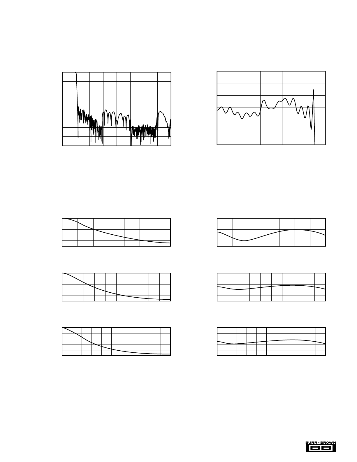
TYPICAL PERFORMANCE CURVES
All specifications at TA = +25°C, VDD = VCC = 5V, SYSCLK = 384fS (fS = 44.1kHz), and 20-bit input data, unless otherwise noted.
DIGITAL FILTER
Digital Filter (De-Emphasis Off, fS = 44.1kHz)
0
–20
–40
–60
–80
–100
Amplitude (dB)
–120
–140
–160
0 0.5 1 1.5 2 2.5 3 3.5 4
DIGITAL FILTER
De-Emphasis Error
DE-EMPHASIS FREQUENCY RESPONSE (fS = 32kHz)
0
–2
–4
–6
Level (dB)
–8
–10
02468101214
FREQUENCY RESPONSE
Frequency (x f
Frequency (kHz)
)
S
0.003
0.002
0.001
0
–0.001
Amplitude (dB)
–0.002
–0.003
0 0.1 0.2 0.3 0.4 0.5
0.5
0.3
0.1
–0.1
Level (dB)
–0.3
–0.5
02468101214
PASSBAND RIPPLE
Frequency (x f
DE-EMPHASIS ERROR (fS = 32kHz)
Frequency (kHz)
)
S
DE-EMPHASIS FREQUENCY RESPONSE (fS = 44.1kHz)
0
–2
–4
–6
Level (dB)
–8
–10
02468101214161820
Frequency (kHz)
DE-EMPHASIS FREQUENCY RESPONSE (fS = 48kHz)
0
–2
–4
–6
Level (dB)
–8
–10
0246810121416182022
Frequency (kHz)
0.5
0.3
0.1
–0.1
Level (dB)
–0.3
–0.5
02468101214161820
0.5
0.3
0.1
–0.1
Level (dB)
–0.3
–0.5
0246810121416182022
DE-EMPHASIS ERROR (fS = 44.1kHz)
Frequency (kHz)
DE-EMPHASIS ERR0R (fS = 48kHz)
Frequency (kHz)
5 PCM1739
®
Page 6

TYPICAL PERFORMANCE CURVES (cont.)
All specifications at TA = +25°C, VDD = VCC = 5V, SYSCLK = 384fS (fS = 44.1kHz), and 20-bit input data, unless otherwise noted.
ANALOG DYNAMIC PERFORMANCE
Supply Voltage Characteristics
TOTAL HARMONIC DISTORTION + NOISE vs V
(VDD = 3.3V)
10
192kHz, 128f
S
1
0.1
0.01
THD+N (%)
44.1kHz, 384f
S
192kHz, 128f
S
0.001
0.0001
44.1kHz, 384f
S
4.0 4.5 5.0 5.5 6.0
V
(V)
CC
SIGNAL-TO-NOISE RATIO vs V
110
(VDD = 3.3V)
108
106
44.1kHz, 384f
S
104
–60dB
0dB
CC
CC
110
108
DYNAMIC RANGE vs V
(VDD = 3.3V)
44.1kHz, 384f
S
CC
106
104
102
100
Dynamic Range (dB)
192kHz, 128f
S
98
96
4.0 4.5 5.0 5.5 6.0
(V)
V
CC
110
CHANNEL SEPARATION vs V
CC
108
106
44.1kHz, 384f
S
104
102
SNR (dB)
192kHz, 128f
S
100
98
96
4.0 4.5 5.0 5.5 6.0
(V)
V
CC
Temperature Characteristics
TOTAL HARMONIC DISTORTION + NOISE
10
1
0.1
0.01
THD+N (%)
0.001
0.0001
4.0 4.5 5.0 5.5 6.0
vs TEMPERATURE
192kHz, 128f
44.1kHz, 384f
44.1kHz, 384f
S
S
192kHz, 128f
S
(V)
V
CC
S
–60dB
0dB
102
100
Channel Separation (dB)
192kHz, 128f
S
98
96
4.0 4.5 5.0 5.5 6.0
VCC (V)
DYNAMIC RANGE vs TEMPERATURE
(V
= 3.3V)
110
108
44.1kHz, 384f
DD
S
106
104
102
100
Dynamic Range (dB)
192kHz, 128f
S
98
96
–25 0 25 50 75 100
Temperature (°C)
®
PCM1739
6
Page 7

TYPICAL PERFORMANCE CURVES (cont.)
CHANNEL SEPARATION vs TEMPERATURE
(V
DD
= 3.3V)
Temperature (°C)
Channel Separation (dB)
110
108
106
104
102
100
98
96
–25 0 25 50 75 100
192kHz, 128f
S
44.1kHz, 384f
S
All specifications at TA = +25°C, VDD = VCC = 5V, SYSCLK = 384fS (fS = 44.1kHz), and 20-bit input data, unless otherwise noted.
Temperature Characteristics (cont.)
SIGNAL-TO-NOISE RATIO vs TEMPERATURE
110
108
106
104
102
SNR (dB)
100
98
96
–25 0 25 50 10075
(V
44.1kHz, 384f
192kHz, 128f
Temperature (°C)
= 3.3V)
DD
S
S
®
7 PCM1739
Page 8
SYSTEM CLOCK AND RESET
FUNCTIONS
SYSTEM CLOCK INPUT
The PCM1739 requires a system clock for operating the
digital interpolation filters and multi-level delta-sigma modulators. The system clock is applied at the SCLK input (pin
5). Table I shows examples of system clock frequencies for
common audio sampling rates.
Figure 1 shows the timing requirements for the system clock
input. For optimal performance, it is important to use a clock
source with low phase jitter and noise. Burr-Brown’s
PLL1700 multi-clock generator is an excellent choice for
providing the PCM1739 system clock.
SYSTEM CLOCK OUTPUT
A buffered version of the system clock input is available at
the CLKO output (pin 4). CLKO operates at the same
frequency as the system clock, SCLK.
POWER-ON AND EXTERNAL RESET FUNCTIONS
The PCM1739 includes a power-on reset function. Figure 2
shows the operation of this function. The system clock input
at SCLK should be active for at least one clock period prior
to VDD = 2.0V. With the system clock active and VDD >
2.0V, the power-on reset function will be enabled. The
initialization sequence requires 1024 system clocks from the
time VDD > 2.0V. The PCM1739 also includes an external
reset capability using the RSTB input (pin 22). This allows
an external controller or master reset circuit to force the
PCM1739 to initialize to its reset default state. For normal
operation, RSTB should be set to a logic ‘1’.
Figure 3 shows the external reset operation and timing. The
RSTB pin is set to logic ‘0’ for a minimum of 20ns. The
RSTB pin is then set to a logic ‘1’ state, which starts the
initialization sequence, which lasts for 1024 system clock
periods.
The external reset is especially useful in applications where
there is a delay between PCM1739 power up and system
clock activation. In this case, the RSTB pin should be held
at a logic ‘0’ level until the system clock has been activated.
SAMPLING
FREQUENCY (f
16kHz — — 4.0960 6.1440 8.1920 12.2880
32kHz — — 8.1920 12.2880 16.3840 24.5760
44.1kHz — — 11.2896 16.9344 22.5792 33.8688
48kHz — — 12.2880 18.4320 24.5760 36.8640
88.2kHz — — 22.5792 33.8688 45.1584 See Note 1
96kHz 12.2880 18.4320 24.5760 36.8640 49.1520 See Note 1
176.4kHz 24.5792 33.8688 See Note 2 See Note 2 See Note 2 See Note 2
192kHz 24.5760 36.8640 See Note 2 See Note 2 See Note 2 See Note 2
NOTES: (1) The 768fS system clock rate is not supported for fS > 64kHz. (2) This system clock rate is not supported for the given sampling frequencies.
) 128f
S
S
192f
S
SYSTEM CLOCK FREQUENCY, f
256f
S
384f
SCLK,
S
(MHZ)
512f
S
768f
TABLE I. System Clock Rates for Common Audio Sampling Frequencies.
t
SCLK
2.0V
0.8V
SCLK
“H”
“L”
t
SCLK
System Clock Pulse Width High t
System Clock Pulse Width Low t
SCLKH
SCLKL
f
SCLK
: 7ns min
: 7ns min
S
FIGURE 1. System Clock Input Timing.
®
PCM1739
8
Page 9

2.4V
= V
2.0V
DD
1.6V
V
CC
Internal Reset
System Clock
(SCLK)
FIGURE 2. Power-On Reset Timing.
RSTB
Internal Reset
System Clock
(SCLK)
NOTE: (1) t
= 20ns min.
RST
FIGURE 3. External Reset Timing.
1024 system clocks
(1)
t
RST
Reset
Reset
1024 system clocks
Reset Removal
Reset Removal
AUDIO SERIAL INTERFACE
The audio serial interface for the PCM1739 is comprised
of a 3-wire synchronous serial port. It includes LRCK (pin
1), BCLK (pin 3), and DATA (pin 2). BCLK is the serial
audio bit clock, and is used to clock the serial data present
on DATA into the audio interface’s serial shift registers.
Serial data is clocked into the PCM1739 on the rising edge
of BCLK. LRCK is the serial audio left/right word clock.
It is used to latch serial data into the serial audio interface’s
internal registers.
Both LRCK and BCLK must be synchronous to the system
clock. Ideally, it is recommended that LRCK and BCLK
be derived from the system clock input or output, SCLK or
CLKO. The left/right clock, LRCK, is operated at the
sampling frequency (fS). The bit clock, BCK, may be
operated at 48 or 64 times the sampling frequency.
AUDIO DATA FORMATS AND TIMING
The PCM1739 supports industry-standard audio data formats, including Standard and I2S. The audio data word
length may be either 24 or 16 bits. Data format and word
length are selected using the FORM and IBIT pins, as
described in the Mode Controls section of this data sheet.
All formats require Binary Two’s Complement, MSB-first
audio data. The data formats are shown in Figure 4, while
Figure 5 shows a detailed timing diagram for the serial
audio interface.
MODE CONTROLS
This section describes the mode control pins used to configure
the operating mode of the PCM1739.
AUDIO DATA FORMAT
The data format used by the audio serial interface is selected
using the FORM input (pin 28). The formats available
include Standard and I2S. Table II shows the FORM pin
configuration.
FORM DATA FORMAT
L Standard
HI
TABLE II. Audio Data Format Selection.
AUDIO DATA WORD LENGTH
The data word length used by the audio serial interface is
selected using the IBIT input (pin 9). The word length may
be either 24 or 16 bits. Table III shows the IBIT pin
configuration.
IBIT DATA WORD LENGTH
L 24 Bits
H 16 Bits
TABLE III. Audio Data Word Length Selection.
2
S
9 PCM1739
®
Page 10

16-Bit Right-Justified
DATA
(2) 16- or 24-Bit I
2
S Data Format; Lch = LOW, Rch = HIGH
(1) Standard Data Format; Lch = HIGH, Rch = LOW
1/f
S
Lch
Rch
LRCK
BCLK
(= 48f
S
or 64f
S
)
1/f
S
Lch
Rch
LRCK
BCLK
(= 48f
S
or 64f
S
)
21
1
2 3
22 23 24
1 2 3
22 23 24
14 15 16 14 15 16
123
DATA
22 23 24 22 23 24
12345
DATA
24-Bit Right-Justified
14 15 16
123
22 23 24
123
45
LSBMSB
LSBMSB
LSBMSB
LSBMSB
LSBMSB
LSBMSB
FIGURE 4. Audio Data Input Formats.
®
PCM1739
10
Page 11

LRCK
BCLK
t
BCH
t
BCY
50% of V
DD
t
BCL
t
BL
t
LB
50% of V
DD
DATA
t
DS
SYMBOL PARAMETER MIN MAX UNITS
t
BCY
t
BCH
t
BCL
t
BL
t
LB
t
DS
t
DH
NOTE: (1) f
is the sampling frequency.
S
BCK Pulse Cycle Time 48 or 64f
BCK High Level Time 35 ns
BCK Low Level Time 35 ns
BCK Rising Edge to LRCK Edge 10 ns
LRCK Falling Edge to BCK Rising Edge 10 ns
DIN Set Up Time 10 ns
DIN Hold Time 10 ns
t
DH
FIGURE 5. Audio Interface Timing.
4x/8x DIGITAL INTERPOLATION
The PCM1739’s digital filter may be configured for either
4x or 8x oversampling. The 8x oversampling setting is
utilized for sampling frequencies up to 96kHz, while 4x
oversampling is utilized for 192kHz operation. The FILT
input (pin 20) is used to select the oversampling rate of the
digital filter. Table IV shows the FILT pin configuration.
FILT OVERSAMPLING RATE
L8x
H 4x ( Required for 192kHz operation)
TABLE IV. Digital Filter Oversampling Rate Selection.
50% of V
DD
(1)
S
sis function is required for proper playback of early audio
compact disks (CDs), which were mastered with signal
emphasis for higher frequencies in the audio band. This was
done to improve the poor high frequency performance of
early CD players. Plots of the de-emphasis filter and error
functions for 32kHz, 44.1kHz, and 48kHz are shown in the
Typical Performance Curves section of this data sheet.
The DEM0 (pin 26) and DEM1 (pin 27) inputs of the
PCM1739 are used to enable and disable the digital deemphasis function. Table VI shows the DEM0 and DEM1
pin configurations.
SOFT MUTE
The Soft Mute function provides for quiet muting of the
DAC outputs, V
L (pin 16) and V
OUT
R (pin 13). This is
OUT
done by ramping an internal digital attenuator from unity
gain to digital mute (all 0’s input to the digital filter). The
MUTE input (pin 21) is used to enable and disable the Soft
Mute function. Table V shows the MUTE pin configuration.
MUTE SOFT MUTE STATUS
L Disabled
H Enabled
TABLE V. Soft Mute Selection.
DIGITAL DE-EMPHASIS
The PCM1739 provides a De-emphasis function for sampling rates equal to 32kHz, 44.1kHz or 48kHz. It is incorporated into the digital filter of the PCM1739. The De-empha-
DEM1 DEM0 DE-EMPHASIS FUNCTION
L L OFF
L H 32kHz De-Emphasis Filter
H L 44.1kHz De-Emphasis Filter
H H 48kHz De-Emphasis Filter
TABLE VI. Digital De-Emphasis.
ANALOG OUTPUTS
The PCM1739 includes two independent output channels;
V
L (pin 16) and V
OUT
outputs, each capable of driving 3.1Vp-p typical into a 5kΩ,
AC-coupled load (VCC = +5V). The internal output amplifiers for V
OUT
L and V
mode (or bipolar zero) voltage, equal to VCC/2.
The output amplifiers include an RC continuous time filter,
which helps to reduce the out-of-band noise energy present
at the DAC outputs due to the noise shaping characteristics
of the PCM1739’s delta-sigma D/A converters. The fre-
11 PCM1739
R (pin 13). These are unbalanced
OUT
R are DC biased to a DC common-
OUT
®
Page 12

quency response of this filter is shown in Figure 6. By itself,
this filter is not enough to attenuate the out-of-band noise to
an acceptable level for most applications. An external lowpass filter is required to provide sufficient out-of-band noise
rejection. Further discussion of DAC post filter circuits is
provided in the Applications Information section of this data
sheet.
20
V
L AND V
COM
R OUTPUTS
COM
Two unbuffered, DC common-mode voltage output pins,
V
L (pin 17) and V
COM
R (pin 12), are brought out for
COM
decoupling purposes. These pins are normally biased to a
DC voltage level equal to VCC/2. These pins may be used to
bias external circuits, but they must be connected to high
impedance nodes. Figure 7 shows examples of the proper use
of the V
COM
L and V
R pins for external biasing applica-
COM
tions.
0
–20
–40
Level (dB)
–60
–80
–100
1 10 100 1k 10k 100k 10M1M
Log Frequency (Hz)
FIGURE 6. Output Filter Frequency Response.
PCM1739
V
OUT
V
COM
x = L or R
(a) Using V
+
R
10µF
10µF
x
x
+
To Bias A Single-Supply Filter Stage
COM
R
2
1
R
C
2
ZERO FLAG OUTPUTS
The PCM1739 includes circuitry for detecting an all zero
data condition for the data input pin, DATA. Zero detection
for each output channel is independent from the other. If the
data for a given channel remains at a ‘0’ level for 1024
sample periods (or LRCK clock periods), a Zero Detect
condition exists for the that channel. Given that a Zero
Detect condition exists, the Zero Flag pin(s) for the corresponding channel(s) will be set to a logic ‘1’ state. The zero
flag outputs include ZEROL (pin 23) and ZEROR (pin 24).
These pins can be used to operate external mute circuits, or
used as status indicators for audio signal processor,
microcontroller, or other digitally-controlled functions.
V
CC
C
1
3
1/2
OPA2353
PCM1739
x = L or R
Filtered
Output
V
CC
x
V
COM
+
10µF
OPA337
Buffered
V
COM
V
CC
V+
PCM1739
x
V
OUT
x
V
COM
x = L or R
(c) Using INA134 for DC-Coupled Output
49.9kΩ
+
10µF
1%
V–
–IN
+IN
25kΩ
25kΩ
FIGURE 7. Biasing External Circuits Using the V
®
PCM1739
25kΩ
INA134
25kΩ
COM
(b) Using a Voltage Follower to Buffer V
Sense
To Low-Pass
Filter Stage
R Pins.
L and V
Out
Ref
COM
12
when Biasing Multiple Nodes
COM
Page 13

APPLICATIONS INFORMATION
CONNECTION DIAGRAM
A basic connection diagram with the necessary power supply bypassing and decoupling components is shown in
Figure 8. Burr-Brown recommends using the component
values shown in Figure 8 for all designs.
The use of series resistors (22Ω to 100Ω) is recommended
for the SCLK, LRCK, BCLK, and DATA inputs. The series
resistor combines with the stray PCB and device input
capacitance to form a low-pass filter, which reduces high
frequency noise emissions and helps to dampen glitches and
ringing present on clock and data lines.
POWER SUPPLIES AND GROUNDING
The PCM1739 requires a +5V analog supply and a +3.3V
digital supply. The +5V supply is used to power the DAC
analog and output filter circuitry, while the +3.3V supply is
used to power the digital filter and logic circuitry. For best
performance, the +3.3V supply should be derived from the
+5V supply using a linear regulator, shown in Figure 8.
Burr-Brown’s REG1117-3.3 is an ideal choice for this application.
Proper power supply bypassing is shown in Figure 8. The
bypass capacitors should be located as close as possible to
the PCM1739 package. The 1µF and 10µF capacitors should
be tantalum or aluminum electrolytic, while the 0.1µF capacitors are ceramic (X7R type is recommended for surface
mount applications).
D/A OUTPUT CIRCUITS
Delta-sigma D/A converters utilize noise-shaping techniques
to improve in-band Signal-to-Noise (SNR) performance at
the expense of generating increased out-of-band noise above
the Nyquist Frequency, or fS/2. The out-of-band noise must
be low-pass filtered in order to provide optimal converter
performance. This is accomplished by a combination of onchip and external low pass filtering.
Figures 7a and 9 show the recommended external low pass
active filter circuits for dual and single-supply applications.
These circuits are 2nd-order filters using the Multiple Feedback (MFB) circuit arrangement, which reduces sensitivity to
passive component variations over frequency and temperature. For more information regarding MFB active filter design,
please refer to Burr-Brown Applications Bulletin AB-034.
From/To
Audio
Source
From
Mode Control
Logic
+3.3V
Regulator
(1)
R
S
C
C
1
+
2
+
C
3
C
4
+
LRCK
DATA
BCLK
CLKO
SCLK
V
SS
V
DD
TEST1
IBIT
V
R
CC
GNDR
V
COM
V
OUT
GNDA
PCM1739
R
R
FORM
DEM1
DEM0
NC
ZEROR
ZEROL
RSTB
MUTE
FILT
L
V
CC
GNDL
V
L
COM
V
L
OUT
V
A
CC
C
5
C
6
+
+
+
+
C
8
Mode Control
From Host Or
Master Reset
Mode Control
C
10
C
9
From
Logic
Zero Flag
Outputs
From
Logic
To
Output
Filter
Circuits
+5V
Analog
FIGURE 8. Basic Connection Diagram.
C
+
C1, C4, C6, C9 = 10µF Tantalum or Aluminum Electrolytic
C
, C5 = 0.1µF Ceramic
2
C
, C10 = 1µF Tanatlum or Aluminum Electrolytic
3
, C8 = 1-10µF Aluminum Electrolytic
C
7
NOTE: (1) R
= 20Ω to 100Ω.
S
13 PCM1739
7
®
Page 14

Since the overall system performance is defined by the
quality of the D/A converters and their associated analog
output circuitry, high quality audio op amps are recommended for the active filters. Burr-Brown’s OPA2134 and
OPA2353 dual op amps are shown in Figures 7a and 9, and
are recommended for use with the PCM1739.
R
2
AV ≈ –
R
2
R
V
IN
1
R
3
C
2
C
1
2
3
OPA2134
R
4
1
R
1
V
OUT
FIGURE 9. Dual Supply Filter Circuit.
PCB LAYOUT GUIDELINES
A typical PCB floor plan for the PCM1739 is shown in
Figure 10. A ground plane is recommended, with the analog
and digital sections being isolated from one another using a
split or cut in the circuit board. The PCM1739 should be
oriented with the digital I/O pins facing the ground plane
split/cut, allowing for direct connection of the digital audio
interface and control signals originating from the digital
section of the board.
Separate power supplies are recommended for the digital
and analog sections of the board. This prevents the switching
noise present on the digital supply from contaminating the
analog power supply and degrading the dynamic performance of the PCM1739. In cases where a common +5V
supply must be used for the analog and digital sections, an
Digital Power
+V
DGND
D
Digital Logic
and
Audio
Processor
DIGITAL SECTION ANALOG SECTION
FIGURE 10. Recommended PCB Layout.
RF Choke or Ferrite Bead
Analog Power
AGND
+5VA +V
REG
V
DD
DGND
Return Path for Digital Signals
Power Supplies
AGND
+5V +V
S
V
PCM1739
AGND
–V
S
–V
S
S
CC
Output
Circuits
Digital
Ground
Analog
Ground
V
DIGITAL SECTION ANALOG SECTION
FIGURE 11. Single-Supply PCB Layout.
®
PCM1739
REG
V
V
DD
DGND
PCM1739
CC
Output
Circuits
AGND
Common
Ground
DD
14
Page 15

0 100 200 300 400 500 600
125
120
115
110
105
100
95
90
85
80
Dynamic Range (dB)
Jitter (ps)
CLOCK JITTER
inductance (RF choke, ferrite bead) should be placed between the analog and digital +5V supply connections to
avoid coupling of the digital switching noise into the analog
circuitry. Figure 11 shows the recommended approach for
single-supply applications
enhanced multi-level delta-sigma architecture also has advantages for input clock jitter sensitivity due to the multilevel quantizer, with the simulated jitter sensitivity shown in
Figure 14.
THEORY OF OPERATION
The delta-sigma section of PCM1739 is based on a 8-level
amplitude quantizer and a 4th-order noise shaper. This
section converts the oversampled input data to 8-level deltasigma format.
A block diagram of the 8-level delta-sigma modulator is
shown in Figure 12. This 8-level delta-sigma modulator has
the advantage of stability and clock jitter sensitivity over the
typical one-bit (2-level) delta-sigma modulator.
The combined oversampling rate of the delta-sigma modulator and the interpolation filter is 64fS for all system clock
combinations (128, 192, 256, 384, 512, 768fS).
The theoretical quantization noise performance of the
8-level delta-sigma modulator is shown in Figure 13. The
4fS or 8f
–1
+
S
Z
–1
+
Z
KEY PERFORMANCE
PARAMETERS AND MEASUREMENT
This section provides information on how to measure key
dynamic performance parameters for the PCM1739. In all
cases, an Audio Precision System Two Cascade or equivalent audio measurement system is utilized to perform the
testing.
TOTAL HARMONIC DISTORTION + NOISE
Total Harmonic Distortion + Noise (THD+N) is a significant figure of merit for audio D/A converters since it takes
into account both harmonic distortion and all noise sources
within a specified measurement bandwidth. The true rms
value of the distortion and noise is referred to as THD+N.
–
+
+
–1
Z
–1
+
Z
FIGURE 12. Eight-Level Delta-Sigma Modulator.
0
–20
–40
–60
–80
–100
Amplitude (dB)
–120
–140
–160
–180
012345678
Frequency (fS)
+
8-Level Quantizer
64f
S
FIGURE 14. Jitter Sensitivity.FIGURE 13. Quantization Noise Spectrum.
15 PCM1739
®
Page 16

For the PCM1739, THD+N is measured with a full scale,
1kHz digital sine wave as the test stimulus at the input of
the DAC. The digital generator is set to 24-bit audio word
length and a sampling frequency of 44.1kHz, 96kHz, or
192kHz. The digital generator output is taken from the
unbalanced S/PDIF connector of the measurement system.
The S/PDIF data is transmitted via a coaxial cable to the
digital audio receiver on the DEM-DAI1739 demo board.
The receiver is then configured to output 24-bit data in
either I2S or left-justified data format. The DAC audio
interface format is programmed to match the receiver
output format. The analog output is then taken from the
DAC post filter and connected to the analog analyzer input
of the measurment system. The analog input is band limited using filters resident in the analyzer. The resulting
THD+N is measured by the analyzer and displayed by the
measurement system.
DYNAMIC RANGE
Dynamic range is specified as A-Weighted, THD+N measured with a –60dBFS, 1kHz digital sine wave stimulus at
the input of the D/A converter. This measurement is de-
signed to give a good indicator of how the DAC will perform
given a low-level input signal.
The measurement setup for the dynamic range measurement
is shown in Figure 15, and is similar to the THD+N test
setup discussed previously. The differences include the
bandlimit filter selection, the additional A-Weighting filter,
and the –60dBFS input level.
IDLE CHANNEL SIGNAL-TO-NOISE RATIO
The SNR test provides a measure of the noise floor of the
D/A converter. The input to the D/A is all 0’s data, and the
D/A converter’s Infinite Zero Detect Mute function must
be disabled (default condition at power up for the PCM1739).
This ensures that the delta-sigma modulator output is connected to the output amplifier circuit so that idle tones (if
present) can be observed and effect the SNR measurement.
The dither function of the digital generator must also be
disabled to ensure an all ‘0’s data stream at the input of the
D/A converter.
The measurement setup for SNR is identical to that used for
dynamic range, with the exception of the input signal level.
(see the notes provided in Figure 16).
Analyzer
and
Display
S/PDIF
Output
Digital
Generator
1kHz Sine Wave
FIGURE 15. Test Setup for THD+N Measurement.
Evaluation Board
DEM-DAI1739
S/PDIF
Receiver
20kHz
Apogee
Filter
Evaluation Board
DEM-DAI1739
S/PDIF
Receiver
PCM1739
HPF = 22Hz
LPF = 30kHz
2nd-Order
Low-Pass
Filter
f
= 54kHz or 108kHz
–3dB
Notch FilterBand Limit
= 1kHzRMS Mode0dBFS,
f
C
PCM1739
(1)
2nd-Order
Low-Pass
Filter
f
= 54kHz or 108kHz
–3dB
Analyzer
and
Display
RMS Mode
S/PDIF
Output
NOTES: (1) Infinite Zero Detect Mute disabled.
(2) Results without A-Weighting will be
approximately 3dB worse.
Digital
Generator
0% Full Scale,
Dither Off (SNR) or
–60dBFS,
1kHz Sine Wave
(Dynamic Range)
FIGURE 16. Test Set-Up for Dynamic Range and SNR Measurements.
®
PCM1739
16
A-Weight
(2)
Filter
HPF = 22Hz
LPF = 22kHz
Notch FilterBand Limit
f
= 1kHz
C
 Loading...