

Page 1

DEM-DAI1681
PCM1681 Evaluation Module
User's Guide
Literature Number: SBAU137
April 2008
Page 2

Submit Documentation Feedback
2 SBAU137 – April 2008
Page 3

SBAU137 – April 2008
Submit Documentation Feedback
Contents
3
Contents
Preface ............................................................................................................................................................ 7
1
Description .......................................................................................................................................... 9
1.1
Functional Block Diagram .................................................................................................................................. 10
1.2
EVM Description ................................................................................................................................................. 10
1.3
Basic Connection and Operation ........................................................................................................................ 11
1.4
EVM Configuration Controls ............................................................................................................................... 11
1.4.1
Jumper Controls ..................................................................................................................................... 11
1.4.2
Switch Controls....................................................................................................................................... 12
1.4.3
DEM-PCM1681 Daughtercard Configuration Controls ........................................................................... 13
1.5
Electrostatic Discharge Warning ........................................................................................................................ 13
1.6
Absolute Maximum Ratings ................................................................................................................................ 14
2
Demonstration Software .................................................................................................................. 15
2.1
Overview ............................................................................................................................................................ 16
2.2
Installation .......................................................................................................................................................... 16
2.3
Using the Demonstration Software ..................................................................................................................... 17
2.3.1
HOLD and PASS .................................................................................................................................... 19
2.3.2
Applicable Function Control .................................................................................................................... 19
3
Typical Performance and Measurement Examples ....................................................................... 21
3.1
Typical Device Performance .............................................................................................................................. 22
3.2
Measurement Examples ..................................................................................................................................... 23
4
Schematic, PCB Layout, and Bill of Materials ............................................................................... 27
4.1
DEM-DAI/MDAC Schematics ............................................................................................................................. 28
4.2
DEM-PCM1681 Schematic ................................................................................................................................. 31
4.3
Printed Circuit Board Layout—DEM-DAI/MDAC ................................................................................................ 32
4.4
Printed Circuit Board Layout—DEM-PCM1681 .................................................................................................. 35
4.5
Component Lists ................................................................................................................................................ 37
4.5.1
Bill of Materials for DEM-DAI/MDAC ...................................................................................................... 37
4.5.2
Bill of Materials for DEM-PCM1681 ........................................................................................................ 39
Important Notices ........................................................................................................................................ 40
Page 4

Submit Documentation Feedback
List of Figures
1-1
DEM-DAI1681 Functional Block Diagram .......................................................................................................... 10
1-2
Jumper JP001 .................................................................................................................................................... 11
2-1
Demonstration Software Window ....................................................................................................................... 17
2-2
Attenuation Control ............................................................................................................................................. 18
2-3
Operation Control ............................................................................................................................................... 18
2-4
Function Control ................................................................................................................................................. 18
3-1
PCM1681 Performance vs fS (Sampling Rate) and f
3-2
THD+N vs Input Level ........................................................................................................................................ 23
3-3 FFT (0 dB) .......................................................................................................................................................... 23
3-4 FFT (–60 dB) ...................................................................................................................................................... 24
3-5 FFT (–90 dB) ...................................................................................................................................................... 24
3-6
FFT (BPZ) .......................................................................................................................................................... 25
3-7
Out-of-Band Noise vs System Clock and Oversampling Condition .................................................................... 25
4-1
Low-Pass Filter Schematic ................................................................................................................................. 28
4-2
Daughtercard Sockets, Connector, and Regulator Schematic ........................................................................... 29
4-3
Digital Audio Interface Schematic ...................................................................................................................... 30
4-4
PCM1681 Daughtercard Schematic ................................................................................................................... 31
4-5
DEM-DAI/MDAC Board Layout—Silkscreen ...................................................................................................... 32
4-6
DEM-DAI/MDAC Board Layout—Top (Component) Side .................................................................................. 33
4-7
DEM-DAI/MDAC Board Layout—Bottom View ................................................................................................... 34
4-8
DEM-PCM1681 Board Layout—Silkscreen ........................................................................................................ 35
4-9
DEM-PCM1681 Board Layout—Top (Component) Side .................................................................................... 35
4-10
DEM-PCM1681 Board Layout—Bottom View .................................................................................................... 36
4 List of Figures SBAU137 – April 2008
(System Clock)............................................................ 22
SYS
www.ti.com
Page 5

Submit Documentation Feedback
www.ti.com
List of Tables
1-1
SW006: Data Format Selection in Hardware Control Mode for PCM1681 ......................................................... 12
1-2
SW006: De-Emphasis and Mute Selection in Hardware Control Mode for PCM1681 ....................................... 12
1-3
SW001/002/003: Format Selection for CS8414 (Digital Audio I/F Receiver) ..................................................... 12
1-4
HDR001: Signal Path Selection for Pin 1 of PCM1681 ...................................................................................... 13
1-5
HDR002: Mode Control Selection of PCM1681 ................................................................................................. 13
1-6
EVM Absolute Maximum Ratings ....................................................................................................................... 14
2-1 Applicable Function Control Summary ............................................................................................................... 19
4-1
Bill of Materials—DEM-DAI/MDAC ..................................................................................................................... 37
4-2
Bill of Materials—DEM-PCM1681 ...................................................................................................................... 39
SBAU137 – April 2008 List of Tables 5
Page 6

Submit Documentation Feedback
6 List of Tables SBAU137 – April 2008
Page 7
Submit Documentation Feedback
About This Manual
This document provides the information needed to set up and operate the DEM-DAI1681, a test platform
for the eight-channel, 24-bit PCM1681
subset of user-programmable functions through a parallel control port, in addition to a full set of
user-programmable functions through a serial control port, SPI™, or I2C™. It also contains instructions to
connect and set up the DEM-DAI1681 for operation, and for the installation and use of the software that
controls the demonstration board. For a more detailed description of the PCM1681 product line, refer to
the product data sheet available from the Texas Instruments web site at http://www.ti.com
documents are listed in the section of this guide entitled Related Documentation from Texas
Instruments.
How to Use This Manual
Throughout this document, the abbreviation EVM and the term evaluation module are synonymous with
the DEM-DAI1681 evaluation module.
Chapter 1 discusses the block diagram and primary features of the DEM-DAI1681. This chapter also
provides general information regarding the default switch and jumper configurations.
Chapter 2 explains how to use the software provided with the DEM-DAI1681.
Chapter 3 presents measured typical performance and characteristic data for the PCM1681 when used
with the DEM-DAI1681.
Chapter 4 includes the EVM electrical schematics, printed circuit board (PCB) layout, and the bills of
materials.
Preface
SBAU137 – April 2008
Read This First
audio digital-to-analog converter (DAC). The PCM1681 provides a
. Support
Information About Cautions and Warnings
This document contains caution statements.
This is an example of a caution statement. A caution statement describes a
situation that could potentially damage your software or equipment.
The information in a caution or a warning is provided for your protection. Please read each caution and
warning carefully.
SYS-2722 is a registered trademark of Audio Precision, Inc.
Microsoft, Windows are registered trademarks of Microsoft Corporation.
SPI is a trademark of Motorola, Inc.
2
I
C is a trademark of NXP Semiconductors.
TOSLINK is a registered trademark of Toshiba Corporation.
All other trademarks are the property of their respective owners.
CAUTION
SBAU137 – April 2008 Read This First 7
Page 8
Submit Documentation Feedback
Data Sheet
Literature Number
Related Documentation From Texas Instruments www.ti.com
Related Documentation From Texas Instruments
The following documents provide information regarding Texas Instruments integrated circuits used in the
assembly of the DEM-DAI1681. These documents are available from the TI web site
the literature number corresponds to the document revision that is current at the time of the writing of this
User’s Guide. Newer revisions may be available from the TI web site at
Texas Instruments Literature Response Center at (800) 477–8924 or the Product Information Center at
(972) 644–5580. When ordering, identify the document(s) by both title and literature number.
PCM1681 Product data sheet SLES211
http://www.ti.com/ or call the
. The last character of
If You Need Assistance
If you have questions regarding either the use of this evaluation module or the information contained in the
accompanying documentation, please contact the Texas Instruments Product Information Center at (972)
644–5580 or visit the TI web site at www.ti.com
FCC Warning
This equipment is intended for use in a laboratory test environment only. It generates, uses, and can
radiate radio frequency energy and has not been tested for compliance with the limits of computing
devices pursuant to subpart J of part 15 of FCC rules, which are designed to provide reasonable
protection against radio frequency interference. Operation of this equipment in other environments may
cause interference with radio communications, in which case the user at his own expense is required to
take whatever measures may be required to correct this interference.
.
Trademarks
All trademarks are the property of their respective owners.
8 Read This First SBAU137 – April 2008
Page 9
SBAU137 – April 2008
Submit Documentation Feedback
Description
11
Chapter 1
SBAU137 – April 2008
Description
The DEM-DAI1681 is an evaluation board for the PCM1681, a 24-bit, 192-kHz, 8-channel audio DAC with
digital audio receiver, 8-channel second-order post filter, mode control interface to a personal computer
(PC), and various switches and jumpers for configuration controls.
The DEM-DAI1681 operates from 5-V and ±15-V analog power supplies with an S/PDIF input signal.
Project collateral discussed in this user’s guide can be downloaded from the following
URL: http://www.ti.com/lit/zip/SBAU137
Topic Page
.
1.1
1.2
1.3
1.4
1.5
1.6
Functional Block Diagram ........................................................................ 10
EVM Description ........................................................................................ 10
Basic Connection and Operation ............................................................ 11
EVM Configuration Controls .................................................................... 11
Electrostatic Discharge Warning ............................................................. 13
Absolute Maximum Ratings ..................................................................... 14
Page 10
10
Description
SBAU137 – April 2008
Submit Documentation Feedback
DEM-DAI/MDAC Motherboard
Ch 7
Ch 8
External-I/F
(CN004)
Ch 5
Ch 6
Ch 3
Ch 4
DAC
PCM1681
CLKO
DATA4
DAI
(Bus)
Select
DIR
Ch 1
Ch 2
2nd-order LPF
L/R
L/R
L/R
L/R
order LPF
(DEM-1681
Daughtercard)
CS8414
Coax
Logic
SCLK
OPT
JUMPER
Format Control
+5 V
3.3 V
REG
SW006
Mode Control Interface to PC
ML MC MDI RST MDO
GND+5 V −15 V GND+15 V
Functional Block Diagram www.ti.com
1.1
Functional Block Diagram
Figure 1-1 illustrates the functional block diagram of the DEM-DAI1681.
M2, M1, M0
-ch
BCLK
and
LRCK
DATA1
DATA2
DATA3
-ch
-ch
-ch
OPA2134
(fC = 54 kHz)
2nd-order LPF
OPA2134
(f
= 54 kHz)
C
2nd-order LPF
OPA2134
= 54 kHz)
(f
C
2nd-
OPA2134
= 54 kHz)
(f
C
1.2
Figure 1-1. DEM-DAI1681 Functional Block Diagram
EVM Description
The DEM-DAI1681 EVM is shipped with the following items:
• EVM Motherboard: DEM-DAI/MDAC
• EVM Daughtercard: DEM-PCM1681
• CD-ROM containing application software, a copy of this user's guide, and a PCM1681 product data
sheet
If any of these items are missing or damaged, please contact your local Texas Instruments representative.
This EVM consists of two PCBs. The DEM-DAI/MDAC motherboard is a common PCB for similar devices
such as the DEM-DAI1608 and the DEM-DAI1680
. The DEM-PCM1681 daughtercard contains the
PCM1681 DAC device, as shown in Figure 1-1.
Page 11
SBAU137 – April 2008
Submit Documentation Feedback
Description
11
www.ti.com Basic Connection and Operation
1.3
Basic Connection and Operation
• Set/confirm jumper JP001 to provide the system clock and other digital signals from the digital audio
receiver to the PCM1681.
• Set/confirm jumper JP201–JP224 to select the cutoff frequency of the second-order post low-pass filter
(LPF) for DAC outputs.
• Set/confirm jumper HDR002 and HDR001 of the PCM1681 daughtercard to select mode control and
coressponding primary pin function.
• Connect the +5-V and ±15-V power supplies to V
, AVCC, –AVCC, and GND on connectors
CC
CN051–CN055.
• Connect the S/PDIF signal into CN001 (COAX) or U001 (OPT).
• Connect the PC printer port to CN003 for mode control, if required.
• Set/confirm the input data format using SW001–SW003 and SW006 (H/W control mode) or the
demonstration software (S/W SPI control).
1.4
EVM Configuration Controls
1.4.1
Jumper Controls
The following jumpers are provided onboard for configuration controls:
• JP001: Set Interface of Digital Signal from DIR to DAC (the device under test [DUT])
The digital signal generated by the digital interface receiver (DIR) is input to this jumper. For each
shorted pin, the corresponding digital signal is applied to the PCM1681. All signals except for BCK and
BCK [L/J] must be shorted for normal operation using the DIR; for BCK and BCK [L/J], one or the other
must be shorted according to the data format selection of the DIR. Figure 1-2 shows jumper JP001.
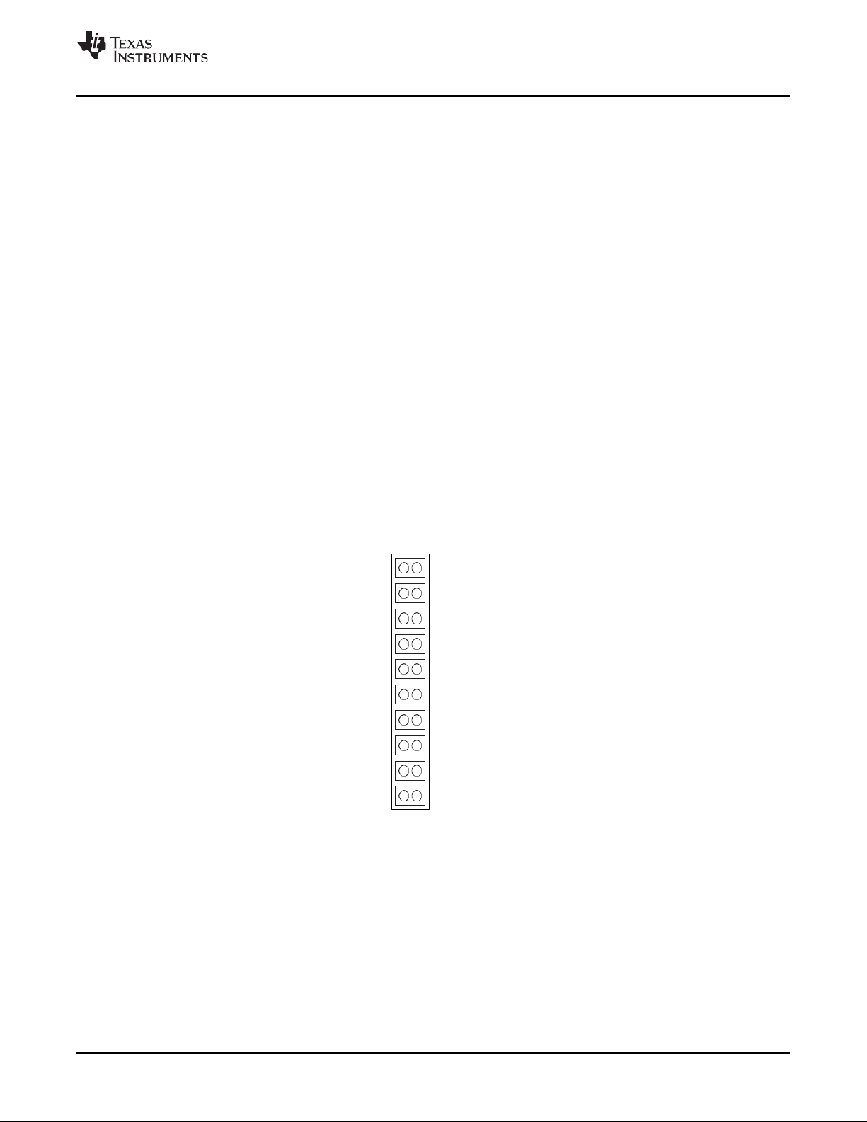
JP001
SCLK
CLKO
GND
BCK
BCK [L/J]
LRCK
DATA1
DATA2
DATA3
DATA4
Figure 1-2. Jumper JP001
• JP201–JP224 (24 Pieces): Set f
These jumpers determine the corner frequency (f
–
JP201–JP224 shorted: fC = 54 kHz for BW = 20 kHz
–
JP201–JP224 open: fC = 108 kHz for BW = 40 kHz
(Corner Frequency) Selection of Second-Order Post LPF
C
) of the second-order post low-pass filter.
C
Page 12
12
Description
SBAU137 – April 2008
Submit Documentation Feedback
Off (H)
On (L)
16-bit to 24-bit, Left-Justified Format
Off (H)
Off (H)
Mute On, De-Emphasis 44.1 kHz On
SW003 (M2)
SW002 (M1)
SW001 (M0)
Data Format Selection
(1)
EVM Configuration Controls www.ti.com
1.4.2
Switch Controls
The following switches, summarized in Table 1-1 to Table 1-3, are provided onboard for EVM control.
Table 1-1. SW006: Data Format Selection in Hardware Control Mode for PCM1681
FMT1 (as S4/ML) FMT0 (as S1/RST) Data Format Selection
On (L) On (L) 24-bit, Right-Justified Format
On (L) Off (H) 16-bit to 24-bit, I2S Format
Off (H) Off (H) 24-bit, I2S Mode TDM Format
Table 1-2. SW006: De-Emphasis and Mute Selection in Hardware Control Mode for PCM1681
MUTE (as S2/MDI) DEMP (as S3/MC) De-Emphasis and Mute Selection
On (L) On (L) Mute Off, De-Emphasis Off
On (L) Off (H) Mute Off, De-Emphasis 44.1 kHz On
Off (H) On (L) Mute On, De-Emphasis Off
Table 1-3. SW001/002/003: Format Selection for CS8414 (Digital Audio I/F Receiver)
L
L
H
(1)
BCK of JP001 selection. When Left-Justified data format is used, move the jumper from BCK to BCK [L/J] for the JP001 setting.
L
H
L
L
16-bit to 24-bit, Left-Justified
L
16-bit to 24-bit, l2S
H
16-bit, Right-Justified
SW004: Manual reset for CS8414
SW005: Digital Audio Interface Selection
• Internal—CS8414
• External—(CN004)
Page 13
SBAU137 – April 2008
Submit Documentation Feedback
Description
13
HDR002
Mode Control of PCM1681
1-2
3-4
5-6
7-8
Open
Open
Open
Short
S/W (SPI) Control Mode
www.ti.com Electrostatic Discharge Warning
1.4.3
DEM-PCM1681 Daughtercard Configuration Controls
This section discusses the headers that are provided as configuration controls for the PCM1681
daughtercard.
1.4.3.1
HDR001: Select Signal Path for Pin 1 of PCM1681
Either 1-2 or 3-2 must be shorted according to the function of pin 1 of the PCM1681, which is determined
by the HDR002 setting. Table 1-4 summarizes the select signal path configuration for HDR002.
Short Open Path for ZR1 output for S/W (SPI and I2C) Control Mode
Open Short Path for FMT0 input for H/W Control Mode
Table 1-4. HDR001: Signal Path Selection for Pin 1 of PCM1681
HDR001
Signal Path for Pin 1 of PCM1681 1-2 3-2
1.4.3.2
HDR002: Select Mode Control of PCM1681
Either 1-2, 3-4, 5-6, or 7-8 must be shorted in order to select mode control type and oversampling
condition of the PCM1681. Table 1-5 summarizes the mode control selection configuration for HDR002.
Table 1-5. HDR002: Mode Control Selection of PCM1681
1.5
Short Open Open Open S/W (I2C) Control Mode
Open Short Open Open H/W Control Mode with Narrow Band Operation
Open Open Short Open H/W Control Mode with Wide Band Operation
Electrostatic Discharge Warning
Many of the components on the DEM-DAI1681 are susceptible to damage by electrostatic discharge
(ESD). Customers are advised to observe proper ESD handling precautions when unpacking and handling
the EVM, including the use of a grounded wrist strap at an approved ESD workstation.
CAUTION
Failure to observe ESD handling procedures may result in damage to EVM
components.
Page 14

14
Description
SBAU137 – April 2008
Submit Documentation Feedback
5-V Power supply CN054
+6
V
Signal Outputs
Line outputs CN201 to CN208
4
V
Absolute Maximum Ratings www.ti.com
1.6
Absolute Maximum Ratings
Table 1-6 summarizes the absolute maximum ratings for the DEM-DAI1681 EVM.
Parameter
Power Supplies
Table 1-6. EVM Absolute Maximum Ratings
DEM-DAI1681 EVM
MIN TYP MAX
UNIT
±15-V Power supply CN051/3
Signal Inputs
S/PDIF input CN001
PC interface input CN003
±18
±2
0
4
V
±
V
V
Page 15

SBAU137 – April 2008
Submit Documentation Feedback
Demonstration Software
15
Chapter 2
SBAU137 – April 2008
Demonstration Software
This chapter provides information regarding the software that is provided with the DEM-DAI1681. The
software allows programming of the PCM1681 internal registers.
Topic Page
2.1
Overview ..................................................................................................... 16
2.2
Installation.................................................................................................. 16
2.3
Using the Demonstration Software ......................................................... 17
Page 16

16
Demonstration Software
SBAU137 – April 2008
Submit Documentation Feedback
Overview
2.1
2.2
www.ti.com
Overview
Use the demonstration software on a personal computer (PC) or lab PC that meets the following
requirements:
®
• Equipped with Microsoft
Windows® operating system (Windows XP or earlier)
• Available printer port
• CD-ROM drive
Installation
First, connect the PC printer port to CN003 on the DEM-DAI1681 using a standard printer cable.
Next, install the demonstration software. The software is distributed on a CD-ROM that is shipped with the
DEM-DAI1681. The software is also available for download from the DEM-DAI1681 product folder
www.ti.com.
To install the software on the PC, first create a new folder on your hard disk drive with an appropriate
name (such as DEM1681). Next, load the CD-ROM into the PC, and navigate to the DEM1681 folder on
the CD-ROM. Copy all the files in the DEM1681 directory to the new folder on the PC.
Open the configuration setting file named dem1608.ini using a text editor, such as Notepad or WordPad.
When the file is open, search for the following command line:
PCMIFADR = &h378
The address &h378 indicates the printer port address that the demonstration software uses to
communicate with the DEM-DAI1681. This address must be set to &h378, &h278, or &h3BC. Most PCs
use &h378 as the default printer port address. If your printer port is not located at &h378, edit the address
to correspond with the PC printer port address.
at
Page 17

SBAU137 – April 2008
Submit Documentation Feedback
Demonstration Software
17
Using the Demonstration Software
www.ti.com
2.3
Using the Demonstration Software
Open the working directory you created on the PC (see the Installation section). Double-click on the
application file named dem1608.exe. A window appears on your desktop screen, as shown in Figure 2-1.
There are two menu selections (Execute and Window) in the menu bar near the top of the window.
Figure 2-1. Demonstration Software Window
The Execute menu includes three selections:
• Initialize instructs the program to write almost of the PCM1681 internal registers with the default values
• Reset instructs the program to rewrite the PCM1681 internal registers with the data currently selected
in the application window
This window and function is not applicable on the PCM1681:
• Exit closes the application
The Window menu includes five options:
• Attenuation control (see Figure 2-2): enables users to control PCM1681 digital attenuation level by
changing the slider position for each channel.
• Operation control (see Figure 2-3): allows users to control mute on/off and DAC operation
enable/disable by channel.
• Function control (see Figure 2-4): controls various programmable functions, such as Interface formats,
oversampling mode, DAC output phase, de-emphasis function/frequency, and so forth. Some functions
are not available for the PCM1681; see Table 2-1 for details.
These windows and functions are not applicable on the PCM1681:
• GPO control
• Register read
Page 18

18
Demonstration Software
SBAU137 – April 2008
Submit Documentation Feedback
Using the Demonstration Software
www.ti.com
Figure 2-2. Attenuation Control Figure 2-3. Operation Control
Figure 2-4. Function Control
Page 19

SBAU137 – April 2008
Submit Documentation Feedback
Demonstration Software
19
Using the Demonstration Software
www.ti.com
Function
PCM1681 Default Setting
Availability on DEM-DAI1681
Digital Attenuation Control, 0 dB to –63 dB
0 dB, No Attenuation
Applicable
(1)
De-Emphasis All Channel Function
De-Emphasis All Channel Disabled
Applicable
De-Emphasis All Channel Sample Rate
44.1 kHz
Applicable
Output Phase Select per Channel
Reverse Phase
Not Applicable
Oversampling Rate Control
Narrow (x64, x32, x16) mode
Applicable
Function
DEM-DAI1681 Default Setting
Availability on PCM1681
Enable Control
2.3.1
HOLD and PASS
Near the top of each window, there is a small button. This button is labeled either HOLD or PASS. You
can toggle the current setting by clicking on this button. When set to HOLD, the settings in an active
window can be changed, but are not written to the register(s) until you press the OK button that appears at
the bottom of the screen.
When the button is set to PASS, any setting changes made in an active window are immediately written to
the corresponding register(s).
2.3.2
Applicable Function Control
Table 2-1 summarizes the various functions of the DEM-DAI1681 and the default settings for each
function. Note that the software is also designed to control the DEM-DAI1608 as well as the
DEM-DAI1681; therefore, there are several inconsistencies between the demonstration software and the
PCM1681 register definitions. Table 2-1 also describes these differences between the software of
DEM-DAI1681 and PCM1681 in detail.
Table 2-1. Applicable Function Control Summary
in 0.5-dB Steps
Soft Mute Control Mute Disabled Applicable
DAC1–8 Operation Control DAC1–8 Enabled Applicable
Audio Data Format Control 16-Bit to 24-Bit Left-Justified Partly Applicable
Digital Filter Roll-Off Control Sharp Roll-Off Applicable
Control
Selection
Output Phase Select Normal Phase Applicable
Zero Flag Polarity Select High Applicable
Software Reset Control Reset Disabled Not Applicable
Digital Filter Roll-Off Control per DATA
Group
Zero Flag Combination Select ZR1: DATA1 Lch
Digital Attenuation Mode Select 0 to –63 dB, 0.5-dB step Not Applicable
Zero Detect Status
(Read-only, I
SCKO Frequency Selection and Output
GPO Output Set and Control Enabled as Zero Flags, not GPOs Not Applicable
Register Read and Address Control Enabled without Auto-Increment Not Applicable
2
C Interface Only)
Slow Roll-Off Not Applicable
Not Applicable
ZR2: DATA1 Rch
Not Applicable Not Applicable
Enabled as SCKO = SCKI Not Applicable
(1)
There is a difference betwen applicable formats and default setting.
Page 20

Submit Documentation Feedback
20 Demonstration Software SBAU137 – April 2008
Page 21

SBAU137 – April 2008
Submit Documentation Feedback
Typical Performance and Measurement Examples
21
Chapter 3
SBAU137 – April 2008
Typical Performance and Measurement Examples
This chapter presents typical performance and a measured data example of the PCM1681 on the DEMPCM1681. The process of measuring dynamic characteristics is also discussed, along with example
®
characteristic data. Performance evaluations used the Audio Precision SYS-2722
Topic Page
3.1
Typical Device Performance .................................................................... 22
3.2
Measurement Examples ........................................................................... 23
audio analyzer.
Page 22

Typical Device Performance
www.ti.com
22
Typical Performance and Measurement Examples
SBAU137 – April 2008
Submit Documentation Feedback
Dynamic
Ch Sep
Gain
Error
THD+N
Gain Error (dB)
THD+N, DR, SNR, Channel Separation (dB)
3.1 Typical Device Performance
Figure 3-1 illustrates a measurement example of PCM1681 performance on a DEM-DAI1681 with default
settings.
PCM1681 PERFORMANCE vs f
110
108
106
104
102
100
98
96
94
92
90
Figure 3-1. PCM1681 Performance vs fS (Sampling Rate) and f
Range
48k
512f
S
SNR
0.5
0.4
0.3
0.2
0.1
0
−0.1
−0.2
−0.3
−0.4
−0.5
(System Clock)
SYS
, f
CONDITION (Narrow)
S
SYS
fS, f
96k
256f
Condition
SYS
S
S
192k
128f
Page 23

Measurement Examples
www.ti.com
SBAU137 – April 2008
Submit Documentation Feedback
Typical Performance and Measurement Examples
23
3.2 Measurement Examples
Figure 3-2 illustrates THD+N performance according to a 1-kHz signal sweep of the digital input level.
Figure 3-2. THD+N vs Input Level
Figure 3-3 through Figure 3-6 show FFT results for full-scale performance and characteristic performance
under a range of conditions. FFT data numbers are 32-k points for all four FFT graphs.
Figure 3-3. FFT (0 dB)
Page 24

24
Typical Performance and Measurement Examples
SBAU137 – April 2008
Submit Documentation Feedback
Measurement Examples
www.ti.com
Figure 3-4. FFT (–60 dB)
Figure 3-5. FFT (–90 dB)
Page 25

SBAU137 – April 2008
Submit Documentation Feedback
Typical Performance and Measurement Examples
25
Measurement Examples
www.ti.com
Figure 3-6. FFT (BPZ)
Figure 3-7shows the out-of-band noise characteristic according to the system clock ratio and oversampling
mode (narrow/wide) setting. A relatively high ratio and wide mode is recommended for lower out-of-band
noise.
Figure 3-7. Out-of-Band Noise vs System Clock and Oversampling Condition
Page 26

Submit Documentation Feedback
26 Typical Performance and Measurement Examples SBAU137 – April 2008
Page 27

SBAU137 – April 2008
Submit Documentation Feedback
Schematic, PCB Layout, and Bill of Materials
27
Chapter 4
SBAU137 – April 2008
Schematic, PCB Layout, and Bill of Materials
This chapter provides the electrical and physical layout information for the DEM-DAI/MDAC and the DEMPCM1681. The bill of materials (BOM) is included for component and manufacturer reference.
Note: Board layouts are not to scale. These are intended to show how the board is laid out; they
are not intended to be used for manufacturing DEM-DAI1681 PCBs.
Topic Page
4.1
4.2
4.3
4.4
4.5
DEM-DAI/MDAC Schematics .................................................................... 28
DEM-PCM1681 Schematic ........................................................................ 31
Printed Circuit Board Layout—DEM-DAI/MDAC .................................... 32
Printed Circuit Board Layout—DEM-PCM1681 ...................................... 35
Component Lists ....................................................................................... 37
Page 28

DEM-DAI/MDAC Schematics
www.ti.com
28
Schematic, PCB Layout, and Bill of Materials
SBAU137 – April 2008
Submit Documentation Feedback
100
4.1
DEM-DAI/MDAC Schematics
The schematic for the sections of the DEM-DAI/MDAC is shown in Figure 4-1 through Figure 4-3.
R205 15k R213 15k
R201
8.2k JP201
V
1
OUT
C201
1200pF
V
2
OUT
R202
8.2k
1200pF
JP202
C202
C207 120pF C217 120pF
C205
2
3
C209
C210
6
5
JP205
120pF
4
JP206
C206 120pF
8
OPA2134A
1
U201
OPA2134A
1/2
7
U201
2/2
R207
Avcc +
Avcc -
100
100
R208
CN201
RCA pj
CN202
RCA
R209
JP207
8.2k
V
3
OUT
C211
1200pF
V
OUT
pj
4
R210
8.2k
C212
1200pF
JP208
JP203
R203
1k
C203
1200pF
R206 15k
JP204
R204
1k
C204
1200pF
10uF/16
10uF/16
C208 120pF
R221 15k
R217
JP213
8.2k
V
5
OUT
C221
1200pF
C223
1200pF
JP215
R219
1k
10uF/16
10uF/16
R222 15k
V
6
OUT
R218
8.2k
C222
1200pF
JP214
C228 120pF
JP216
R220
1k
C224
1200pF
C225
2
3
C229
C230
6
5
JP217
120pF
4
JP218
C226 120pF
8
OPA2134A
2/2
R223
1
U203
OPA2134A
1/2
Avcc +
Avcc -
7
U203
C227 120pF C237 120pF
100
R224
CN205
RCA
CN206
RCA
V
OUT
pj
7
V
pj
OUT
8
R225
JP219
8.2k
C231
1200pF
R226
8.2k
C232
1200pF
JP220
C213
1200pF
R214 15k
C214
1200pF
C233
1200pF
R230 15k
C234
1200pF
JP209
R211
1k
JP210
R212
1k
JP221
R227
1k
JP222
R228
1k
C215
2
3
C219
10uF/16
C220
10uF/16
C218 120pF
6
5
R229 15k
C235
2
3
C239
10uF/16
C240
10uF/16
C238 120pF
6
5
JP211
120pF
U202
4
OPA2134A
JP212
C216 120pF
8
OPA2134A
2/2
JP223
120pF
U204
4
JP224
C236 120pF
8
OPA2134A
2/2
R215
100
1
1/2
Avcc +
Avcc -
7
U202
R216
100
R231
100
1
OPA2134A
1/2
Avcc +
Avcc -
7
U204
R232
100
CN203
CN207
RC A pj
CN204
RC A
RC A pj
CN208
RC A pj
pj
Figure 4-1. Low-Pass Filter Schematic
Page 29

SBAU137 – April 2008
Submit Documentation Feedback
Schematic, PCB Layout, and Bill of Materials
29
RST
ML
MC
MDI
MDO
(NC)
(NC)
GND
VCC
R106
R108
R110
R112
10 k
10 k
GND
ZFLG/GPO1
ZFLG/GPO2
ZFLG/GPO3
ZFLG/GPO4
ZFLG/GPO5
ZFLG/GPO6
ZFLG8
GND
ZFLGA
ZFLG/GPO1
ZFLG/GPO2
ZFLG/GPO3
ZFLG/GPO4
ZFLG/GPO5
ZFLG/GPO6
ZFLG7 ZFLG8
www.ti.com DEM-DAI/MDAC Schematics
V
DD
U051
MDO
MDI
MC
ML
RST-
SCLK
CLKO
GND
BCK
LRCK
DATA1
DATA2
DATA3
DATA4
C101
10uF
R101
R102
R103
/16V
R104
R105
R107
R109
R111 22
REG1117-3.3
2 OUT IN 3
C056
10µF
/16V
CN104
22
22
22
22
22
22
22
V
CC
GND
1
V
DD
C055
0.1µF
C051
0.1µF
C102
GND
SCKI
SCKO
GND
BCK
LRCK
DIN1
DIN2
DIN3
DIN4
CN055
banana jack
(black)
C052
100µF
/16V
10µF
/16V
CN054
banana jack
(red)
VCC
10 k 10 k
banana jack
CN053
banana jack
(blue)
C053
100µF
/16V
CN101
CN102
V
1
OUT
V
2
OUT
GND
V
3
OUT
V
4
OUT
GND
V
5
OUT
V
6
OUT
GND
V
7
OUT
V
8
OUT
GND
CN103
CN052
(green)
CN051
banana jack
(orange)
C054
100µF
/16V
AVCC+
AVCC-
V
1
OUT
2
V
OUT
V
3
OUT
V
4
OUT
V
5
OUT
V
6
OUT
V
7
OUT
V
8
OUT
CN105
ZFLGA
ZFLG7
Figure 4-2. Daughtercard Sockets, Connector, and Regulator Schematic
Page 30

DEM-DAI/MDAC Schematics
www.ti.com
30
Schematic, PCB Layout, and Bill of Materials
SBAU137 – April 2008
Submit Documentation Feedback
21 22
CS8414
[e-SCLK] [e-BCK] [e-LRCK] [e-DATA]
57LE-40360-7700(D3)
(L001)
CN001
RCA pj
V
CC
2 4 5 6
U001
TORX173
3
1
R001
C002
0.01uF
C004
C003
0.1uF
10uF
/16V
C001
0.01uF
75
[e-SCLK]
[e-BCK]
[e-LRCK]
[e-DATA]
1
C005
10uF
/16V
DAI select
INT(CS8414)
EXT
(FIL001)
3 IN OUT 2
GND
1 2 3 4 5 6 7 8 9 10 11 12 13 14 15 16 17 18 19 20 21 22 23 24
25 26 27 28 29 30 31 32 33 34 35 36 37 38 39 40 41 42 43 44 45 46 47 48
C006
0.1uF
CN003
SW005
FT2D-2M
(C016)
0.1uF
1 2 3 4 5
19
20 23 24 25 26 27 28 2 9
SW006
DSS104
1
C
2
Cd/F1
3
Cc/F0
4
Cb/E2
5
Ca/E1
6
C0/E0
7
VD+
8
DGND
9
RXP
10
RXN
11
FSYNC
12
SCK
13
CS12/FCK
14
U
[SCLK]
[BCK]
[LRCK] 7
[DATA]
(C015)
100uF/16V
1
2
3
4
U002
VERF
Ce/F2
SDATA
ERF
M1
M0
VA+
AGND
FILT
MCK
M2
M3
SEL
CBL
C013 0.1uF
1
2 19
3 18
4 17
5 16
6 15
8
9
10
GND
6 7 8
9 10 11 12 13 14 15 16 17 18
RA001
47k x5
CN002
FFC-2BMEP1
28
27
26
25
24
23
C008
0.1uF
22
21
20
19
18
17
16
15
0.068uF
20
Vcc
14
13
12
11
U005
74VHC244
30 31 32 33 34 35 36
74VHC244
C007
10uF
/16V
R002
470
C009
[BCK]
[SCLK]
[BCK]
[LRCK]
[DATA]
(CN004)
FFC-48BMEP1
V
DD
C014 0.1uF
U006
1
[RST-]
2
[MDO]
3
[MDI]
4
5
[MC]
6
7
[ML]
8
9 12
10
GND
C011 0.1uF
U004 74HCT32
1
2 13
3 12
4 11
5 10
6 9
7 8
GND
C010 0.1uF
U003 74VHC14
1
2
3
4
5
6
7
GND
SW001 SW002 SW003
FT1D-2M FT1D-2M FT1D-2M
[SCLK]
[CLKO]
[GND]
[BCK]
[BCK(INV)]
[LRCK]
[DATA1]
[DATA2]
[DATA3]
[DATA4]
JP001
FFC-20BMEP1
20
Vcc
19
18
17
16
15
14
13
11
14
Vcc
14
Vcc
13
12
11
10
9
8
RST-
R003
47k
C012
10uF
/16V
LRCK
MDO
MDI
MC
ML
D001
1SS133
SCLK
CLKO
GND
BCK
DATA1
DATA2
DATA3
DATA4
R004
470
SW004
FP1F
-2M
Figure 4-3. Digital Audio Interface Schematic
Page 31

SBAU137 – April 2008
Submit Documentation Feedback
Schematic, PCB Layout, and Bill of Materials
31
www.ti.com DEM-PCM1681 Schematic
4.2
DEM-PCM1681 Schematic
Figure 4-4 illustrates the schematic for the DEM-PCM1681.
Figure 4-4. PCM1681 Daughtercard Schematic
Page 32

32
Schematic, PCB Layout, and Bill of Materials
SBAU137 – April 2008
Submit Documentation Feedback
Printed Circuit Board Layout—DEM-DAI/MDAC
www.ti.com
4.3
Printed Circuit Board Layout—DEM-DAI/MDAC
Figure 4-5 through Figure 4-7 illustrate the printed circuit board (PCB) layout for the DEM-DAI/MDAC.
Figure 4-5. DEM-DAI/MDAC Board Layout—Silkscreen
Page 33

SBAU137 – April 2008
Submit Documentation Feedback
Schematic, PCB Layout, and Bill of Materials
33
www.ti.com Printed Circuit Board Layout—DEM-DAI/MDAC
Figure 4-6. DEM-DAI/MDAC Board Layout—Top (Component) Side
Page 34

34
Schematic, PCB Layout, and Bill of Materials
SBAU137 – April 2008
Submit Documentation Feedback
Printed Circuit Board Layout—DEM-DAI/MDAC
www.ti.com
Figure 4-7. DEM-DAI/MDAC Board Layout—Bottom View
Page 35

SBAU137 – April 2008
Submit Documentation Feedback
Schematic, PCB Layout, and Bill of Materials
35
www.ti.com Printed Circuit Board Layout—DEM-PCM1681
4.4
Printed Circuit Board Layout—DEM-PCM1681
Figure 4-8 through Figure 4-10 illustrate the PCB layout for the DEM-PCM1681.
Figure 4-8. DEM-PCM1681 Board Layout—Silkscreen
Figure 4-9. DEM-PCM1681 Board Layout—Top (Component) Side
Page 36

36
Schematic, PCB Layout, and Bill of Materials
SBAU137 – April 2008
Submit Documentation Feedback
Printed Circuit Board Layout—DEM-PCM1681
www.ti.com
Figure 4-10. DEM-PCM1681 Board Layout—Bottom View
Page 37

SBAU137 – April 2008
Submit Documentation Feedback
Schematic, PCB Layout, and Bill of Materials
37
Component Lists
www.ti.com
Qty
RefDes
Description
Size
Mfr Part Number
MFR
1
C009
Film Capacitor
0.068µF
AMFF0050J683
Nissei
16
C205, C206, C207,
Film Capacitor
120pF
APSF0100J121
Nissei
1
CN052
Banana Jack
Green
T-45
Sato Parts
1
CN053
Banana Jack
Blue
T-45
Sato Parts
1
CN105
Pin Header
10 Pins
FFC-10AMEP1
Honda
CN205, CN207
4.5
4.5.1
Component Lists
Bill of Materials for DEM-DAI/MDAC
Table 4-1 lists the bill of materials for the DEM-DAI/MDAC.
Table 4-1. Bill of Materials—DEM-DAI/MDAC
2
C001, C002 Film Capacitor
13
C003, C005,
C007,C101, C102,
C209,C210, C219,
C220,C229, C230,
C239, C240
4
C004, C006,
C008,C016, C051
5
C010, C011, C013,
C014, C055
1
C012 Aluminum Electrolytic Capacitor
3
C015, C052, C053,
C054
1
C056 Tantalum Electrolytic Capacitor
16
C201, C202, C203,
C204, C211, C212,
C213, C214, C221,
C222, C223, C224,
C231, C232, C233,
C234
Aluminum Electrolytic Capacitor
Film Capacitor
Ceramic Capacitor
Aluminum Electrolytic Capacitor
Film Capacitor 1200pF APSF0100J122 Nissei
0.01µF
10µF/16V
0.1µF
0.1µF
10µF/16V
100µF/16V
10µF/16V
AMFF0050J103 Nissei
Electric
ROA-16V100M ELNA
AMFF0050J104 Nissei
Electric
Electric
D55Y5V1H104Z51 NEC
SME16VB10M Nippon
ChemiCon
ROA-16V101M ELNA
DN1C100M1S NEC
Electric
C208, C215, C216,
C217, C218, C225,
C226, C227, C228,
C235, C236, C237,
C238
1
CN001 RCA Connector Yellow LPR6520-0804 SMK
1
CN002 Pin Header 2 Pins FFC-2BMEP1 Honda
1
CN003 Ribbon Connector 36 Pins, Right
1
CN051 Banana Jack Orange T-45 Sato Parts
1
CN054 Banana Jack Red T-45 Sato Parts
1
CN055 Banana Jack Black T-45 Sato Parts
2
CN101, CN103 Connector 10 Pins Z-220-10FD Honda
1
CN102 Connector 12 Pins Z-220-12FD Honda
1
CN104 Connector 11 Pins Z-220-11FD Honda
4
CN201, CN203,
4
CN202, CN204,
CN206, CN208
1
D001 Diode
1
JP001 Pin Header 20 pins FFC-20BMEP1 Honda
RCA Connector White LPR6520-0803 SMK
RCA Connector Red LPR6520-0802 SMK
Angle
57LE40360-7700(D3) DDK
1SS133 ROHM
Electric
Page 38

38
Schematic, PCB Layout, and Bill of Materials
SBAU137 – April 2008
Submit Documentation Feedback
2
R002, R004
Metal Film Resistor
470, 1/4W, F
SN14C2C
KOA
1
R003
Metal Film Resistor
47k, 1/4W, F
SN14C2C
KOA
R109, R111
8
R205, R206, R213,
Metal Film Resistor
15k, 1/4W, F
SN14C2C
KOA
8
R207, R208, R215,
Metal Film Resistor
100, 1/4W, F
SN14C2C
KOA
1
SW006
DIP Switch
4 Poles
DSS104
Fujisoku
2
U005, U006
Bus Buffer
TC74VHC244F
Toshiba
Component Lists www.ti.com
Qty RefDes Description Size Mfr Part Number MFR
24
JP201 to JP224 Pin Header 2 pins FFC-2BMEP1 Honda
1
R001 Metal Film Resistor 75, 1/4W, F SN14C2C KOA
8
R101, R102, R103,
R104, R105, R107,
4
R106, R108, R110,
R112
8
R201, R202, R209,
R210, R217, R218,
R225, R226
8
R203, R204, R211,
R212, R219, R220,
R227, R228
R214, R221, R222,
R229, R230
R216, R223, R224,
R231, R232
1
RA001 Resistor Array 47k x 5, J M6-1-473J Beckman
3
SW001, SW002,
SW003
1
SW004 Push Switch
1
SW005 Toggle Switch DPDT FT2D-2M Fujisoku
Table 4-1. Bill of Materials—DEM-DAI/MDAC (continued)
Metal Film Resistor 22, 1/4W, F SN14C2C KOA
Metal Film Resistor 10k, 1/4W, F SN14C2C KOA
Metal Film Resistor 8.2k, 1/4W, F SN14C2C KOA
Metal Film Resistor 1k, 1/4W, F SN14C2C KOA
Toggle Switch SPDT FT1D-2M Fujisoku
FP1F-2M Fujisoku
1
U001 Optical Transmitter TOSLINK
1
U002 Digital Audio I/F Receiver IC
1
U003 Schmitt Trigger Inv
1
U004 Quad 2-Input OR gate
1
U051 3.3-V Regulator
4
U201, U202, U203,
IC Socket DIP 8 pins ICC09-308-396C KEL
U204
4
Spacer
®
TORX179P Toshiba
CS8414-CS Cirrus Logic
TC74VHC14F Toshiba
TC74HCT32AF Toshiba
REG1117-3.3 Texas
Instruments
AR-325B
Page 39

SBAU137 – April 2008
Submit Documentation Feedback
Schematic, PCB Layout, and Bill of Materials
39
Component Lists
www.ti.com
13
C002, C004, C006,
Aluminum Electrolytic Capacitor
10µF/16V
R3A-16V100M
ELNA
1
HDR002
Pin Header
8 Pins
FFC-8BMEP1
Honda
1
RA001
Network Resistor
220k x2 (1608),
MNR12E0ABJ224
ROHM
4.5.2
Bill of Materials for DEM-PCM1681
Table 4-2 lists the bill of materials for the DEM-PCM1681.
Table 4-2. Bill of Materials—DEM-PCM1681
Qty RefDes Description Size Mfr Part Number MFR
5
C001, C003, C005,
C007, C009
C008, C010, C011
to C018
2
CN001, CN003 Pin Header 10 Pins FFC-10AMEP1 Honda
1
CN002 Pin Header 12 Pins FFC-12AMEP1 Honda
1
CN004 Pin Header 11 Pins FFC-11AMEP1 Honda
1
HDR001 Pin Header 3 Pins FFC-3AMEP1 Honda
1
U001 Audio DAC 24-bits, 192
Ceramic Capacitor
0.1µF (2125)
J
kHz, 8-ch
GRM21BB11H104KA0 1 Murata
PCM1681PWP Texas
Instruments
Page 40

EVALUATION BOARD/KIT IMPORTANT NOTICE
Texas Instruments (TI) provides the enclosed product(s) under the following conditions:
This evaluation board/kit is intended for use for ENGINEERING DEVELOPMENT, DEMONSTRATION, OR EVALUATION PURPOSES
ONLY and is not considered by TI to be a finished end-product fit for general consumer use. Persons handling the product(s) must have
electronics training and observe good engineering practice standards. As such, the goods being provided are not intended to be complete
in terms of required design-, marketing-, and/or manufacturing-related protective considerations, including product safety and environmental
measures typically found in end products that incorporate such semiconductor components or circuit boards. This evaluation board/kit does
not fall within the scope of the European Union directives regarding electromagnetic compatibility, restricted substances (RoHS), recycling
(WEEE), FCC, CE or UL, and therefore may not meet the technical requirements of these directives or other related directives.
Should this evaluation board/kit not meet the specifications indicated in the User’s Guide, the board/kit may be returned within 30 days from
the date of delivery for a full refund. THE FOREGOING WARRANTY IS THE EXCLUSIVE WARRANTY MADE BY SELLER TO BUYER
AND IS IN LIEU OF ALL OTHER WARRANTIES, EXPRESSED, IMPLIED, OR STATUTORY, INCLUDING ANY WARRANTY OF
MERCHANTABILITY OR FITNESS FOR ANY PARTICULAR PURPOSE.
The user assumes all responsibility and liability for proper and safe handling of the goods. Further, the user indemnifies TI from all claims
arising from the handling or use of the goods. Due to the open construction of the product, it is the user’s responsibility to take any and all
appropriate precautions with regard to electrostatic discharge.
EXCEPT TO THE EXTENT OF THE INDEMNITY SET FORTH ABOVE, NEITHER PARTY SHALL BE LIABLE TO THE OTHER FOR ANY
INDIRECT, SPECIAL, INCIDENTAL, OR CONSEQUENTIAL DAMAGES.
TI currently deals with a variety of customers for products, and therefore our arrangement with the user is not exclusive.
TI assumes no liability for applications assistance, customer product design, software performance, or infringement of patents or
services described herein.
Please read the User’s Guide and, specifically, the Warnings and Restrictions notice in the User’s Guide prior to handling the product. This
notice contains important safety information about temperatures and voltages. For additional information on TI’s environmental and/or
safety programs, please contact the TI application engineer or visit www.ti.com/esh
.
No license is granted under any patent right or other intellectual property right of TI covering or relating to any machine, process, or
combination in which such TI products or services might be or are used.
FCC Warning
This evaluation board/kit is intended for use for ENGINEERING DEVELOPMENT, DEMONSTRATION, OR EVALUATION PURPOSES
ONLY and is not considered by TI to be a finished end-product fit for general consumer use. It generates, uses, and can radiate radio
frequency energy and has not been tested for compliance with the limits of computing devices pursuant to part 15 of FCC rules, which are
designed to provide reasonable protection against radio frequency interference. Operation of this equipment in other environments may
cause interference with radio communications, in which case the user at his own expense will be required to take whatever measures may
be required to correct this interference.
EVM WARNINGS AND RESTRICTIONS
It is important to operate this EVM within the input voltage range of –2.0 V to +4.0 V and the output voltage range of –4.0 V to +4.0 V.
Exceeding the specified input range may cause unexpected operation and/or irreversible damage to the EVM. If there are questions
concerning the input range, please contact a TI field representative prior to connecting the input power.
Applying loads outside of the specified output range may result in unintended operation and/or possible permanent damage to the EVM.
Please consult the EVM User's Guide prior to connecting any load to the EVM output. If there is uncertainty as to the load specification,
please contact a TI field representative.
During normal operation, some circuit components may have case temperatures greater than +60°C. The EVM is designed to operate
properly with certain components above +60°C as long as the input and output ranges are maintained. These components include but are
not limited to linear regulators, switching transistors, pass transistors, and current sense resistors. These types of devices can be identified
using the EVM schematic located in the EVM User's Guide. When placing measurement probes near these devices during operation,
please be aware that these devices may be very warm to the touch.
Mailing Address: Texas Instruments, Post Office Box 655303, Dallas, Texas 75265
Copyright © 2008, Texas Instruments Incorporated
Page 41

IMPORTANT NOTICE AND DISCLAIMER
TI PROVIDES TECHNICAL AND RELIABILITY DATA (INCLUDING DATASHEETS), DESIGN RESOURCES (INCLUDING REFERENCE
DESIGNS), APPLICATION OR OTHER DESIGN ADVICE, WEB TOOLS, SAFETY INFORMATION, AND OTHER RESOURCES “AS IS”
AND WITH ALL FAULTS, AND DISCLAIMS ALL WARRANTIES, EXPRESS AND IMPLIED, INCLUDING WITHOUT LIMITATION ANY
IMPLIED WARRANTIES OF MERCHANTABILITY, FITNESS FOR A PARTICULAR PURPOSE OR NON-INFRINGEMENT OF THIRD
PARTY INTELLECTUAL PROPERTY RIGHTS.
These resources are intended for skilled developers designing with TI products. You are solely responsible for (1) selecting the appropriate
TI products for your application, (2) designing, validating and testing your application, and (3) ensuring your application meets applicable
standards, and any other safety, security, or other requirements. These resources are subject to change without notice. TI grants you
permission to use these resources only for development of an application that uses the TI products described in the resource. Other
reproduction and display of these resources is prohibited. No license is granted to any other TI intellectual property right or to any third
party intellectual property right. TI disclaims responsibility for, and you will fully indemnify TI and its representatives against, any claims,
damages, costs, losses, and liabilities arising out of your use of these resources.
TI’s products are provided subject to TI’s Terms of Sale (www.ti.com/legal/termsofsale.html) or other applicable terms available either on
ti.com or provided in conjunction with such TI products. TI’s provision of these resources does not expand or otherwise alter TI’s applicable
warranties or warranty disclaimers for TI products.
Mailing Address: Texas Instruments, Post Office Box 655303, Dallas, Texas 75265
Copyright © 2019, Texas Instruments Incorporated
 Loading...