

Page 1

PCIE16X-800EVK User Guide
PCIe 16X Lane Card Evaluation Kit
General Description:
The PCIE16X-800EVK is a PCIe add-in riser card for PCIe 16x applications. It provides a complete
platform to evaluate 4 - DS80PCI800SQ, 8 channels PCIe repeater for PCIe system protocol and lane
negotiation validation. The card has a 16X PCIe edge fingers at J1 which plugs into a motherboard
that has a PCIe 16X connector. The card also has a PCIe 16X connector at J2 for endpoint connection
(PCIe graphic card or SATA/SAS raid controller card).
Features:
■ 8 channel PCIe repeater up to 8 Gbps (GEN 3)
■ Low power consumption, with option to power down unused channels
■ Adjustable receive equalization
■ Adjustable transmit VOD and De-emphasis
■ IDLE detection — squelch function auto mutes the output
■ Programmable via pin selection or SMBus interface
■ Single supply operation: VIN = 3.3V±10% or VDD = 2.5V ±5%
■ -40°C to +85°C Operation
■ >6 kV HBM ESD Rating
■ High speed signal flow–thru pin-out package - SQA54A: 54-pin LLP (10 mm x 5.5 mm, 0.5 mm pitch)
Applications:
■ Extends FR-4 Backplane Trace for PCIe Applications
PCIE16X-800EVK Demo Kit Contents:
■ End User License Agreement
■ PCIE16X-800EVK User Guide Rev 1.2
■ PCIE16X-800EVK Board
Odering Information:
SMA Evaluation Kit: PCIE16X-800EVK
© Texas Instruments 2011
www.ti.com
Page 2
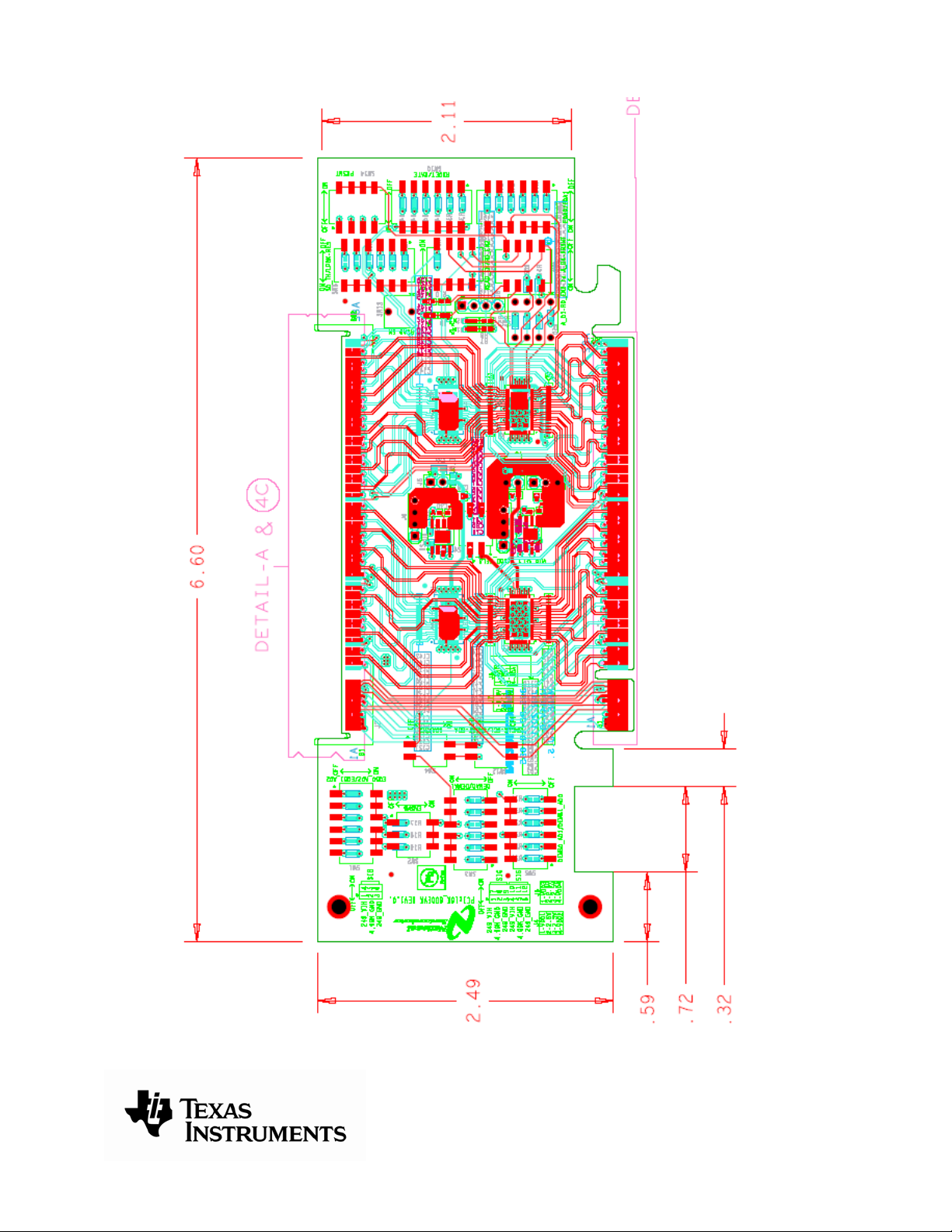
Figure 1. PCIE16X-800EVK Evaluation Board
© Texas Instruments 2011
www.ti.com
Page 3

Table 1. Switches to set the 4-level input control pins
4 – level Input Settings
0 – Tie 249 ohm to GND ON – OFF – OFF
R – Tie 5k ohm to GND OFF – ON – OFF
F – FLOAT (open) OFF – OFF – OFF
1 – Tie 249 ohm to VIH OFF – OFF – ON
The following switches are used to set the input condition for the 4-level inputs:
SW1, SW2, SW3, SW5, SW6, SW10, SW11.
There are 3 switches connected to an input signal pin. Each switch when set to the ON position sets the pin to
one of the 4-level setting. The 6 pin switches are assigned similar to the 3 pin switches. The only difference is 2
signal pins are connected and thus 6-5-4 is for the one signal pin and 3-2-1 is for another signal pin. Please note
only 1 switch at the ON position is allowed.
Table 2. Connection and Control Description
Component Name
J1 PCIE TX/RX High speed differential TX/RX from/to Root Complex
J2 PCIE TX/RX High speed differential TX/RX to/from End Point
J3, J5 3.3V to VIN
J4, J6 2.5V to VDD
J7 VIN or VDD Jumper VIH: set 1-2 = VIN (3.3V) or set 2-3 = VDD (2.5V)
J8 SDA, SCL
J9 EEPROM Optional socket for EEPROM
Function
3.3V DC Power – VIN to DS80PCI800SQ
Jumper ON = 3.3V mode operation
Jumper OFF = 2.5V mode operation
2.5V DC Power – VDD to DS80PCI800SQ
Jumper ON (1-2, 3-4) = 2.5V mode operation
Jumper OFF (1-2, 3-4) = 3.3V mode operation
Optional SMBUS access pins.
See the datasheet for additional information on SMBUS.
Setting for 3 pin switches (3-2-1)
SW1
SW2
SW3
SW4 SDA/SCL “ON” position connects SDA and SCL lines to the device pin.
SW5
SW6
SW7
EQB[1:0] or
AD[3:2]
ENSMB
DEMA[1:0]
DEMB[1:0] or
AD[1:0]
SD_TH and
LPBK - RES
VDD_SEL1_2
VDD_SEL3_4
READ_EN,
SW8
RD_EN2,
RD_EN3 and
RD_EN4
A_D1 to
SW9
SW10
SW11
RD_EN2 …
A_D3 to
RD_EN4
RXDET and
RATE
EQA[1:0]
PIN MODE – EQ control for channel B inputs
SMBUS MODE – AD[3:2] device address bits
ENSMB = LOW – PIN MODE
ENSMB = HIGH – SMBUS (slave mode)
ENSMB = FLOAT – SMBUS (master mode – load configuration from EEPROM)
PIN MODE – DE control for channel A outputs
PIN MODE – DE control for channel B outputs
SMBUS MODE – AD[1:0] device address bits
SD_TH – Signal detect threshold level (FLOAT = Default level)
LPBK function for PCI402 and RESERVED for PCI800 (FLOAT = Normal operation)
VDD_SEL – Enable or disable the internal 3.3V to 2.5V regulator for U1 and U2.
ON connects to GND to enable the internal LDO regulator for 3.3V mode operation.
For manual control of loading the external EEPROM and daisy chain the READ_EN
to the ALL_DONE pins.
Pin1 = ON connects the SW13 push button to the READ_EN of U1.
Pin2,3,4 = OFF
Pin1 = ON connects the ALL_DONE of U1 to READ_EN of U2.
Pin2 = ON connects the ALL_DONE of U2 to READ_EN of U3.
Pin3 = ON connects the ALL_DONE of U3 to READ_EN of U4.
Pin4 = OFF
RXDET – Input internal 50 ohm to VDD terminations
RXDET = F (AUTO RX Detect), RXDET = 1 (50 ohm input termination).
RATE = 0 (GEN1,2) = 2.5G / 5.0G.
RATE = R (GEN3) = 8.0G.
RATE = F (AUTO Detect). The RATE auto detect circuit requires the idle and active
signal which occurs during the link training negotiation.
PIN MODE – EQ control for channel A inputs
© Texas Instruments 2011
www.ti.com
Page 4

SW12
SW13 READ_EN
SW14 PRSNT
SDA/SCL to
SMCLK/SMDAT
“ON” connect the SDA/SCL bus to the PCIe SMCLK and SMDAT bus.
Default is “OFF”.
ENSMB = FLOAT – SMBUS (master mode – load configuration from EEPROM)
SW6: SD_TH becomes the READ_EN pin.
To start the loading at power up, set SW6 pin 3 to “ON” position (pull to GND).
To manually control the start, set SW6 to “OFF” position and set SW8 pin1 to “ON”
and pin2 to “OFF” position and push the SW13 button for the high to low transition to
start the loading. When the loading is complete the LEDs – D1 thru D4 light should
turn OFF.
“ON” connects the PCIe PRSNT signal to the device PRSNT pin.
For 16X, set all the switches to the “ON” position.
Quick Start User Guide:
1. Connect J1 – PCIe 16x edge finger to the motherboard (root complex)
2. Connect J2 - PCIe 16x connector to an add-in card (end point).
3. For 3.3V mode operation, set J3 jumper to ON and do not use J4 (leave jumper OFF).
For 2.5V mode operation, set J3 jumper to OFF and set J4 jumper to ON (1-2 and 3-4).
4. Set jumper – J7 for VIH connection to VIN (3.3V) or VDD (2.5V). Default is 1-2 set to ON for VIH = 3.3V.
5. Set SW7 – VDD_SEL1_2 and VDD_SEL3_4 to “ON” position for 3.3V mode operation.
6. Set the control pins for normal operation
SW10 – RXDET = F (continuous receiver detection): set switches (3-2-1) = (OFF-OFF-OFF).
RXDET = 1 (50 ohm input termination): set switches (3-2-1) = (OFF-OFF-ON).
SW10 – RATE = F (enable rate detection): set switches (6-5-4) to (OFF-OFF-OFF).
RATE = R (GEN3 mode): set switches (6-5-4) = (OFF-ON-OFF).
RATE = 0 (GEN1,2 mode): set switches (6-5-4) = (ON-OFF-OFF).
SW6 – SD_TH = F (default signal detect threshold level): set switches (3-2-1) = (OFF-OFF-OFF).
SW6 – LPBK - RES = F (normal operation): set switches (6-5-4) = (OFF-OFF-OFF).
SW8: Set switches to “OFF” position.
SW9: Set switches to “OFF” position.
SW14 – PRSNT = GND (enables the device): set switches to “ON” position.
5. Set the input equalization level.
For external pin mode control of the equalization level:
Set ENSMB = 0 (1kohm to GND) by using the SW2 (3-2-1) = (ON-OFF-OFF).
SW4 pin1,2 must be set to the OFF positions, so the SMBUS signals are disconnected.
Refer to Table 1 for information on the 3 switch settings for the 4 level input.
Example:
Set EQB[1:0] with SW1 for the B bank of inputs (top 2 left inputs of DS80PCI800).
SW1 (6-5-4),(3-2-1) = (OFF-ON-OFF), (OFF-ON-OFF) = EQB[1:0] = R,R = 14.6 dB at 4 GHz (level 6).
Set EQA[1:0] with SW11 for the A bank of inputs (bottom 2 left inputs of DS80PCI800).
SW8 (6-5-4),(3-2-1) = (OFF-ON-OFF), (OFF-ON-OFF) = EQA[1:0] = R,R = 14.6 dB at 4 GHz (level 6).
The table below is the 16 possible EQ settings when in pin mode.
Level EQA/B[1:0]
6 5 4 3 2 1
1 0, 0
2 0, R
3 0, F
4 0, 1
5 R, 0 OFF
6 R, R OFF
7 R, F OFF
SW1 - EQB[1:0]
SW11 - EQA[1:0] EQ (dB) at 4 GHz
ON
ON
ON
ON
OFF OFF
OFF OFF OFF
OFF OFF OFF OFF OFF 9.9
OFF OFF OFF OFF
ON
ON
ON
OFF
OFF OFF
OFF OFF OFF OFF 17.0
ON
ON
OFF OFF 4.9
ON
OFF OFF 14.3
ON
OFF 7.9
ON
OFF 14.6
11.0
© Texas Instruments 2011
www.ti.com
Page 5

8 R ,1 OFF
9 F ,0 OFF OFF OFF
10 F, R OFF OFF OFF OFF
11 F, F OFF OFF OFF OFF OFF OFF 24.4
12 F, 1 OFF OFF OFF OFF OFF
13 1, 0 OFF OFF
14 1, R OFF OFF
15 1, F OFF OFF
16 1, 1 OFF OFF
6. Set the output VOD and De-emphasis level.
For external pin mode control for the VOD and De-emphasis level (Gen1&2 only):
Set ENSMB = 0 (1kohm to GND) by using the SW2 (3-2-1) = (ON-OFF-OFF).
SW4 pin1,2 must be set to the OFF positions, so the SMBUS signals are disconnected.
Refer to Table 1 for information on the 3 switch settings for the 4 level input.
Example:
Set DEMB[1:0] with SW5 for the B bank of outputs (top 2 right outputs of DS80PCI800).
SW5 (6-5-4),(3-2-1) = (ON-OFF-OFF), (OFF-OFF-ON) = DEMB[1:0] = 0,1 (VOD=1.0V, DE=0 dB).
Set DEMA[1:0] with SW3 for the A bank of outputs (bottom 2 right outputs of DS80PCI800).
SW3 (6-5-4),(3-2-1) = (ON-OFF-OFF), (OFF-OFF-ON) = DEMA1:0] = 0,1 (VOD=1.0V, DE=0 dB).
The table below is the 16 possible settings of VOD and DE when in pin mode.
In Gen 1/2, the de-emphasis level can be set with the DEMx[1:0] pins, but is not available in Gen 3.
Level DEMA/B[1:0]
6 5 4 3 2 1 VOD (Vp-p) DE (dB)
1 0, 0
2 0, R
3 0, F
4 0, 1
5 R, 0 OFF
6 R, R OFF
7 R, F OFF
8 R ,1 OFF
9 F ,0 OFF OFF OFF
10 F, R OFF OFF OFF OFF
11 F, F OFF OFF OFF OFF OFF OFF 1.2
12 F, 1 OFF OFF OFF OFF OFF
13 1, 0 OFF OFF
14 1, R OFF OFF
15 1, F OFF OFF
16 1, 1 OFF OFF
ON
ON
ON
ON
ON
OFF OFF
OFF OFF OFF
OFF OFF OFF OFF OFF 0.9
OFF OFF OFF OFF
ON
ON
ON
ON
OFF OFF OFF
ON
ON ON
ON
ON
ON
SW5 - DEMB[1:0]
SW3 - DEMA[1:0]
OFF
OFF OFF
OFF OFF OFF OFF 1.1
OFF OFF OFF
ON ON
ON
ON
ON
OFF
OFF OFF OFF 31.4
OFF OFF
ON
ON
ON
OFF
OFF OFF OFF 1.3
OFF OFF
OFF OFF 18.0
ON
OFF OFF 27.4
ON
OFF OFF 0.8
ON
OFF OFF 1.0
ON
OFF OFF 1.1
ON
OFF OFF 1.3
ON
For SMBUS mode control of the EQ, VOD and De-emphasis level:
Set ENSMB = 1 (1kohm to VIH) by using the SW2 (3-2-1) = (OFF-OFF-ON).
Set SW4 pin1,2 to the ON position so the SMBUS signals are connected.
Set SW3 pin1 thru pin6 switches to the OFF position so they do not connect to the SDA and SCL line.
Set the SW1 and SW5 for the AD[3:0] pins. AD[3:0]=0000 sets device slave address = B0’hex.
Connect SDA, SCL and GND to J17. Please refer to datasheet for register map for EQ, VOD and DEM.
ON
OFF 22.0
ON
OFF 29.0
ON
OFF 0.9
ON
OFF 1.0
ON
OFF 1.2
ON
OFF 1.3
ON
1.0
1.1
1.2
1.3
18.5
25.8
32.7
GEN1,2
0
0
‐3.5
0
‐3.5
‐6
0
‐3.5
‐6
0
‐3.5
‐6
0
‐3.5
‐6
‐9
© Texas Instruments 2011
www.ti.com
Page 6

Document ID: PCIE16X-800EVK User Guide
Date: November, 2011
Rev: 1.2
© Texas Instruments 2011
www.ti.com
Page 7

5
12V
B1
12V
B2
12V
B3
GND
GND
3_3V
GND
C31 0.22uF
C32 0.22uF
GND
GND
C33 0.22uF
C34 0.22uF
GND
GND
C35 0.22uF
C36 0.22uF
GND
GND
C37 0.22uF
C38 0.22uF
GND
GND
C39 0.22uF
C40 0.22uF
GND
GND
C41 0.22uF
C42 0.22uF
GND
GND
C43 0.22uF
C44 0.22uF
GND
GND
C45 0.22uF
C46 0.22uF
GND
GND
C47 0.22uF
C48 0.22uF
GND
GND
C49 0.22uF
C50 0.22uF
GND
GND
C51 0.22uF
C52 0.22uF
GND
GND
C53 0.22uF
C54 0.22uF
GND
GND
C55 0.22uF
C56 0.22uF
GND
GND
C57 0.22uF
C58 0.22uF
GND
GND
C59 0.22uF
C60 0.22uF
GND
GND
C61 0.22uF
C62 0.22uF
GND
B10
B11
B12
B13
B14
B15
B16
B17
B18
B19
B20
B21
B22
B23
B24
B25
B26
B27
B28
B29
B30
B31
B32
B33
B34
B35
B36
B37
B38
B39
B40
B41
B42
B43
B44
B45
B46
B47
B48
B49
B50
B51
B52
B53
B54
B55
B56
B57
B58
B59
B60
B61
B62
B63
B64
B65
B66
B67
B68
B69
B70
B71
B72
B73
B74
B75
B76
B77
B78
B79
B80
B81
B82
B4
B5
B6
B7
B8
B9
SMCLK
SMDAT
JTAG1
3_3VAUX
D D
WAKE
RSVD1
PETp0
PETn0
PRSNT2_1
PETp1
PETn1
PETp2
PETn2
PETp3
PETn3
RSV2
PRSNT2_2
PETp4
C C
PETn4
PETp5
PETn5
PETp6
PETn6
PETp7
PETn7
PRSNT2_3
PETp8
PETn8
PETp9
PETn9
B B
PETp10
PETn10
PETp11
PETn11
PETp12
PETn12
PETp13
PETn13
PETp14
PETn14
PETp15
PETn15
A A
PRSNT2_4
RSVD2
A1
A1
B1
A2
A2
B2
A3
A3
B3
A4
A4
B4
A5
A5
B5
A6
A6
B6
A7
A7
B7
A8
A8
B8
A9
A9
B9
A10
A10
B10
A11
A11
B11
A12
A12
B12
A13
A13
B13
A14
A14
B14
A15
A15
B15
A16
A16
B16
A17
A17
B17
A18
A18
B18
A19
A19
B19
A20
A20
B20
A21
A21
B21
A22
A22
B22
A23
A23
B23
A24
A24
B24
A25
A25
B25
A26
A26
B26
A27
A27
B27
A28
A28
B28
A29
A29
B29
A30
A30
B30
A31
A31
B31
A32
A32
B32
A33
A33
B33
A34
A34
B34
A35
A35
B35
A36
A36
B36
A37
A37
B37
A38
A38
B38
A39
A39
B39
A40
A40
B40
A41
A41
B41
A42
A42
B42
A43
A43
B43
A44
A44
B44
A45
A45
B45
A46
A46
B46
A47
A47
B47
A48
A48
B48
A49
A49
B49
A50
A50
B50
A51
A51
B51
A52
A52
B52
A53
A53
B53
A54
A54
B54
A55
A55
B55
A56
A56
B56
A57
A57
B57
A58
A58
B58
A59
A59
B59
A60
A60
B60
A61
A61
B61
A62
A62
B62
A63
A63
B63
A64
A64
B64
A65
A65
B65
A66
A66
B66
A67
A67
B67
A68
A68
B68
A69
A69
B69
A70
A70
B70
A71
A71
B71
A72
A72
B72
A73
A73
B73
A74
A74
B74
A75
A75
B75
A76
A76
B76
A77
A77
B77
A78
A78
B78
A79
A79
B79
A80
A80
B80
A81
A81
B81
A82
A82
B82
J1
PCIE_16X_EDGE_FINGER
5
12V
12V
GND
3_3V
3_3V
GND
GND
C63 0.22uF
C64 0.22uF
GND
GND
C65 0.22uF
C66 0.22uF
GND
GND
C67 0.22uF
C68 0.22uF
GND
GND
C69 0.22uF
C70 0.22uF
GND
GND
C71 0.22uF
C72 0.22uF
GND
GND
C73 0.22uF
C74 0.22uF
GND
GND
C75 0.22uF
C76 0.22uF
GND
GND
C77 0.22uF
C78 0.22uF
GND
GND
C79 0.22uF
C80 0.22uF
GND
GND
C81 0.22uF
C82 0.22uF
GND
GND
C83 0.22uF
C84 0.22uF
GND
GND
C85 0.22uF
C86 0.22uF
GND
GND
C87 0.22uF
C88 0.22uF
GND
GND
C89 0.22uF
C90 0.22uF
GND
GND
C91 0.22uF
C92 0.22uF
GND
GND
C93 0.22uF
C94 0.22uF
GND
PRSNT1
JTAG2
JTAG3
JTAG4
JTAG5
PERST
REFCLKp
REFCLKn
PERp0
PERn0
RSVD
PERp1
PERn1
PERp2
PERn2
PERp3
PERn3
RSVD3
RSVD4
PERp4
PERn4
PERp5
PERn5
PERp6
PERn6
PERn7
RSVD5
PERp8
PERn8
PERp9
PERn9
PERp10
PERn10
PERp11
PERn11
PERp12
PERn12
PERp13
PERn13
PERp14
PERn14
PERp15
PERn15
PRSNT2_2
PRSNT2_3
PRSNT2_4
PRSNT2_1
PRSNT2_2
PRSNT2_3
PRSNT2_4
EQB0_AD3
46
EQB1_AD2
47
ENSMB
48
DEMA0_SDA
49
DEMA1_SCL
50
VDD1
51
PRSNT
52
DEMB0_AD1
53
DEMB1_AD0
54
GND
55
U1
DS80PCI800
PLACE CLOSE TO PIN
VDD1
GND
C25
0.01uF
GND
3_3
VPERp7
C23
GND
4.7uF
EQB0_AD3
46
EQB1_AD2
47
ENSMB
48
DEMA0_SDA
49
DEMA1_SCL
50
VDD2
51
PRSNT
52
DEMB0_AD1
53
DEMB1_AD0
54
GND
55
U2
DS80PCI800
PLACE CLOSE TO PIN PLACE CLOSE TO PIN
4
VDD1
PETn0_C
PETp0_C
PETn1_C
PETp1_C
PETn2_C
PETp2_C
4544434241403938373635343332313029
VDD
OB_0-
OB_1-
EQB0/AD3
EQB1/AD2
ENSMB
DEMA0/SDA
DEMA1/SCL
VDD
/PRSNT
DEMB0/AD1
DEMB1/AD0
DAP
OB_0+
IB_0+
OB_2-
OB_1+
OB_2+
IB_0-
IB_1+
IB_1-
IB_2+
IB_2-
IB_3+
1234567891011121314151617
PETp0
PETn0
PETn1
PETp1
PETp3
PETp2
PETn2
0.1uF
GND
9
DAP
S_DWN
NC2
ADJ
C4
C3
0.1uF
8
7
6
C2
C1
0.1uF
U5
1
BYPASS
2
NC1
3
GND
4 5
INPUT OUTPUT
LP3878-ADJ
PETp9_C
PETn8_C
PETp8_C
PETn9_C
VDD2
PETn10_C
PETp10_C
4544434241403938373635343332313029
VDD
OB_0-
OB_1-
EQB0/AD3
EQB1/AD2
ENSMB
DEMA0/SDA
DEMA1/SCL
VDD
/PRSNT
DEMB0/AD1
DEMB1/AD0
DAP
OB_0+
IB_0+
OB_2-
OB_1+
OB_2+
IB_0-
IB_1+
IB_1-
IB_2+
IB_2-
IB_3+
1234567891011121314151617
PETp8
PETn9
PETn8
PETp9
PETp10
PETp11
PETn10
VDD2
93614 5141 93614 5141
C7
C6
GND
0.1uF
4
VDD1
PETp3_C
PETn3_C
PETn4_C
PETp4_C
PETp5_C
PETn5_C
VDD
OB_3-
OA_0-
VDD1
OA_1-
OA_0+
OA_1+
VDD
IA_0+
IA_0-
IA_1+
IA_1-
VDD
VDD1
PETn4
PETp4
PETp5
PETn5
OB_3+
IB_3-
PETn3
C5
0.1uF
0.1uF
3_3V
R3
51k
PETn12_C
PETn13_C
PETn11_C
PETp13_C
VDD2
PETp12_C
PETp11_C
VDD
OB_3-
OA_0-
VDD2
OA_1-
OA_0+
OA_1+
VDD
IA_0+
IA_0-
IA_1+
IA_1-
VDD
VDD2
PETp13
PETn13
PETn12
PETp12
OB_3+
IB_3-
PETn11
C8
0.1uFC90.1uF
0.1uF
PETn6_C
PETp6_C
PETp7_C
PETn7_C
28
OA_2-
OA_2+
OA_3+
ALL_DONE
SD_TH/RD_EN
IA_2+
IA_2-
IA_3+
18
PETn6
PETp6
PETn7
PETp7
C27 10uF
GND
C29 1nF
R2
1k
R1 1.5k
PETp14_C
PETp15_C
PETn14_C
PETn15_C
28
OA_2-
OA_2+
OA_3+
ALL_DONE
SD_TH/RD_EN
IA_2+
IA_2-
IA_3+
18
PETp15
PETp14
PETn15
PETn14
C10
0.1uF
3
12
R7
220
A_D1
SD_TH
VDD_SEL1_2
VIN1_2
RES
RXDET
RATE
EQA0
EQA1
SMCLKPRSNT2_1
SMDAT
SD_TH
RD_EN2
RD_EN3
RD_EN4
A_D1
A_D2
A_D3
A_D4
GND GND
D1
SML-P12PTT86
OA_3-
27
26
25
VDD_SEL
24
VIN
23
RES
22
RXDET
21
RATE
20
EQA0
19
EQA1
IA_3-
J3 (U1,U2):
1-2 (ON) FOR 3.3V,
1-2 (OFF) FOR 2.5V.
J4 (U1,U2):
1-2, 3-4 (ON) FOR 2.5V,
1-2, 3-4 (OFF) FOR 3.3V.
J3
2 HEADER
3_3V
1
VIN1_2
OA_3-
VDD_SEL
VIN
RES
RXDET
RATE
EQA0
EQA1
IA_3-
2
VOUT1_2
VDD1
VOUT1_2
VDD2
GND
27
26
25
24
23
22
21
20
19
EQB0_AD3
EQB1_AD2
ENSMB
DEMA0_SDA
DEMA1_SCL
PRSNT
DEMB0_AD1
DEMB1_AD0
EQA1
EQA0
RATE
RXDET
RES
VDD_SEL1_2
VDD_SEL3_4
3_3V
GND
10uF
1
2
3
4
J4
4 HEADER
D2
SML-P12PTT86
12
R8
220
A_D2
RD_EN2
VDD_SEL1_2
VIN1_2
RES
RXDET
RATE
EQA0
EQA1
C21
1uF
VOUT1_2
EQB0_AD3
EQB1_AD2
ENSMB
DEMA0_SDA
DEMA1_SCL
PRSNT
DEMB0_AD1
DEMB1_AD0
EQA1
EQA0
RATE
RXDET
RES
VDD_SEL1_2
VDD_SEL3_4
3_3V
SMCLK
SMDAT
SD_TH
RD_EN2
RD_EN3
RD_EN4
A_D1
A_D2
A_D3
A_D4
EQB0_AD3
EQB1_AD2
ENSMB
DEMA0_SDA
DEMA1_SCL
VDD3
PRSNT
DEMB0_AD1
DEMB1_AD0
GND
U3
DS80PCI800
PLACE CLOSE TO PIN
C160
C26
0.01uF
GND
3_3V
C24
4.7uF
EQB0_AD3
EQB1_AD2
ENSMB
DEMA0_SDA
DEMA1_SCL
VDD4
PRSNT
DEMB0_AD1
DEMB1_AD0
GND
U4
DS80PCI800
3
46
EQB0/AD3
47
EQB1/AD2
48
ENSMB
49
DEMA0/SDA
50
DEMA1/SCL
51
VDD
52
/PRSNT
53
DEMB0/AD1
54
DEMB1/AD0
55
DAP
VDD3
9 1436415193614 5141
C11
GND
0.1uF
U6
1
BYPASS
2
NC1
3
GND
4 5
INPUT OUTPUT
GND
LP3878-ADJ
46
EQB0/AD3
47
EQB1/AD2
48
ENSMB
49
DEMA0/SDA
50
DEMA1/SCL
51
VDD
52
/PRSNT
53
DEMB0/AD1
54
DEMB1/AD0
55
DAP
PERp2
PERn2
VDD3
VDD3
PERn0
PERn1
PERp0
PERp1
PERp3
PERn3
PERp4
PERn4
PERp5
4544434241403938373635343332313029
VDD
OB_0-
OB_1-
OB_0+
OB_1+
IB_0+
IB_0-
IB_1+
IB_1-
VDD
OB_2-
OB_3-
OB_2+
IB_2+
IB_2-
OA_0-
OB_3+
OA_0+
IB_3+
IB_3-
VDD
IA_0+
IA_0-
IA_1+
1234567891011121314151617
PERp0_C
C12
PERp8
PERn0_C
PERp1_C
0.1uF
GND
9
DAP
S_DWN
PERp9
PERn8
PERn1_C
C13
NC2
ADJ
PERn9
PERp2_C
0.1uF
VDD4
PERp3_C
8
7
6
PERp10
PERn10
C14
PERn3_C
0.1uF
PERp11
PERn5_C
PERp5_C
PERp4_C
PERn4_C
C15
0.1uF
3_3V
R6
51k
PERn11
PERn12
PERp13
PERp12
VDD4
VDD3
PERn2_C
4544434241403938373635343332313029
VDD
OB_0-
OB_1-
OB_0+
OB_1+
IB_0+
IB_0-
IB_1+
IB_1-
VDD
OB_2-
OB_3-
OB_2+
IB_2+
IB_2-
OA_0-
OB_3+
OA_0+
IB_3+
IB_3-
VDD
IA_0+
IA_0-
IA_1+
1234567891011121314151617
PERp9_C
PERn9_C
PERn11_C
PERp8_C
PERn8_C
VDD4
PERp10_C
PERn10_C
PERp12_C
PERp11_C
PERn12_C
PERp13_C
PERn13_C
VDD4
GND
C16
0.1uF
C17
0.1uF
C18
0.1uF
PERn5
PERp6
OA_1-
OA_1+
IA_1-
VDD
VDD3
PERp6_C
GND
R5
1k
PERn13
PERp14
OA_1-
OA_1+
IA_1-
VDD
VDD4
PERp14_C
C19
0.1uF
2
PERp7
PERn6
PERn7
28
OA_2-
OA_3-
OA_2+
OA_3+
ALL_DONE
SD_TH/RD_EN
VDD_SEL
IA_2+
IA_2-
IA_3+
IA_3-
18
PERn7_C
PERn6_C
PERp7_C
J5
2 HEADER
C28 10uF
C30 1nF
R4 1.5k
PERp15
PERn15
PERn14
28
OA_2-
OA_3-
OA_2+
OA_3+
ALL_DONE
SD_TH/RD_EN
VDD_SEL
IA_2+
IA_2-
IA_3+
IA_3-
18
PERn15_C
PERp15_C
PERn14_C
C20
0.1uF
2
SML-P12PTT86
RXDET
RATE
EQA0
EQA1
SML-P12PTT86
RXDET
RATE
EQA0
EQA1
1
B10
B11
B12
B13
B14
B15
B16
B17
B18
B19
B20
B21
B22
B23
B24
B25
B26
B27
B28
B29
B30
B31
B32
B33
B34
B35
B36
B37
B38
B39
B40
B41
B42
B43
B44
B45
B46
B47
B48
B49
B50
B51
B52
B53
B54
B55
B56
B57
B58
B59
B60
B61
B62
B63
B64
B65
B66
B67
B68
B69
B70
B71
B72
B73
B74
B75
B76
B77
B78
B79
B80
B81
B82
J2
B1
B1
B2
B2
B3
B3
B4
B4
B5
B5
B6
B6
B7
B7
B8
B8
B9
B9
A10
B10
A11
B11
A12
B12
A13
B13
A14
B14
A15
B15
A16
B16
A17
B17
A18
B18
A19
B19
A20
B20
A21
B21
A22
B22
A23
B23
A24
B24
A25
B25
A26
B26
A27
B27
A28
B28
A29
B29
A30
B30
A31
B31
A32
B32
A33
B33
A34
B34
A35
B35
A36
B36
A37
B37
A38
B38
A39
B39
A40
B40
A41
B41
A42
B42
A43
B43
A44
B44
A45
B45
A46
B46
A47
B47
A48
B48
A49
B49
A50
B50
A51
B51
A52
B52
A53
B53
A54
B54
A55
B55
A56
B56
A57
B57
A58
B58
A59
B59
A60
B60
A61
B61
A62
B62
A63
B63
A64
B64
A65
B65
A66
B66
A67
B67
A68
B68
A69
B69
A70
B70
A71
B71
A72
B72
A73
B73
A74
B74
A75
B75
A76
B76
A77
B77
A78
B78
A79
B79
A80
B80
A81
B81
A82
B82
1
NWE82DHRN-T9410
12V
12V
D3
12
R9
220
A_D3
27
RD_EN3
26
VDD_SEL3_4
25
VIN3_4
24
VIN
RES
J5 (U3,U4):
1-2 (ON) FOR 3.3V,
1-2 (OFF) FOR 2.5V.
J6 (U3,U4):
1-2, 3-4 (ON) FOR 2.5V,
1-2, 3-4 (OFF) FOR
3.3V.
23
22
21
20
19
1
2
VDD3
VOUT3_4
VDD4
GND
RES
RXDET
RATE
EQA0
EQA1
3_3V
VIN3_4
C22
GND
10uF
1
2
3
4
4 HEADER
C161
1uF
J6
D4
12
R10
220
A_D4
27
RD_EN4
26
VDD_SEL3_4
25
VIN3_4
24
RES
VIN
RES
23
RXDET
22
RATE
21
EQA0
20
EQA1
19
Title
PCIE16X_800EVK
Size Document Number Rev
DS80PCI800 PCIE 16X CARD PAGE 1 A
B
SMCLK
AT
SMD
JTAG1
3_3VAUX
WAKE
RSVD1
PETp0_C
PETn0_C
PRSNT2_1
PETp1_C
PETn1_C
PETp2_C
PETn2_C
PETp3_C
PETn3_C
RSV2
PRSNT2_2
PETp4_C
PETn4_C
PETp5_C
PETn5_C
PETp6_C
PETn6_C
PETp7_C
PETn7_C
PRSNT2_3
PETp8_C
PETn8_C
PETp9_C
PETn9_C
PETp10_C
PETn10_C
PETp11_C
PETn11_C
PETp12_C
PETn12_C
PETp13_C
PETn13_C
PETp14_C
PETn14_C
PETp15_C
PETn15_C
PRSNT2_4
RSVD2
12V
GND
GND
3_3V
GND
C95 0.22uF
C96 0.22uF
GND
GND
C97 0.22uF
C98 0.22uF
GND
GND
C99 0.22uF
C1000.22uF
GND
GND
C1010.22uF
C1020.22uF
GND
GND
C1030.22uF
C1040.22uF
GND
GND
C1050.22uF
C1060.22uF
GND
GND
C1070.22uF
C1080.22uF
GND
GND
C1090.22uF
C1100.22uF
GND
GND
C1110.22uF
C1120.22uF
GND
GND
C1130.22uF
C1140.22uF
GND
GND
C1150.22uF
C1160.22uF
GND
GND
C1170.22uF
C1180.22uF
GND
GND
C1190.22uF
C1200.22uF
GND
GND
C1210.22uF
C1220.22uF
GND
GND
C1230.22uF
C1240.22uF
GND
GND
C1250.22uF
C1260.22uF
GND
Date: Sheet
C1270.22uF
C1280.22uF
C1290.22uF
C1300.22uF
C1310.22uF
C1320.22uF
C1330.22uF
C1340.22uF
C1350.22uF
C1360.22uF
C1370.22uF
C1380.22uF
C1390.22uF
C1400.22uF
C1410.22uF
C1420.22uF
C1430.22uF
C1440.22uF
C1450.22uF
C1460.22uF
C1470.22uF
C1480.22uF
C1490.22uF
C1500.22uF
C1510.22uF
C1520.22uF
C1530.22uF
C1540.22uF
C1550.22uF
C1560.22uF
C1570.22uF
C1580.22uF
11Thursday, December 09, 2010
PRSNT1
12V
12V
GND
JTAG2
JTAG3
JTAG4
JTAG5
3_3V
3_3
V
PERST
GND
REFCLKp
REFCLKn
GND
PERp0_C
PERn0_C
GND
RSVD
GND
PERp1_C
PERn1_C
GND
GND
PERp2_C
PERn2_C
GND
GND
PERp3_C
PERn3_C
GND
RSVD3
RSVD4
GND
PERp4_C
PERn4_C
GND
GND
PERp5_C
PERn5_C
GND
GND
PERp6_C
PERn6_C
GND
GND
PERp7_C
PERn7_C
GND
RSVD5
GND
PERp8_C
PERn8_C
GND
GND
PERp9_C
PERn9_C
GND
GND
PERp10_C
PERn10_C
GND
GND
PERp11_C
PERn11_C
GND
GND
PERp12_C
PERn12_C
GND
GND
PERp13_C
PERn13_C
GND
GND
PERp14_C
PERn14_C
GND
GND
PERp15_C
PERn15_C
GND
of
A1
A1
A2
A2
A3
A3
A4
A4
A5
A5
A6
A6
A7
A7
A8
A8
A9
A9
A10
A11
A12
A13
A14
A15
A16
A17
A18
A19
A20
A21
A22
A23
A24
A25
A26
A27
A28
A29
A30
A31
A32
A33
A34
A35
A36
A37
A38
A39
A40
A41
A42
A43
A44
A45
A46
A47
A48
A49
A50
A51
A52
A53
A54
A55
A56
A57
A58
A59
A60
A61
A62
A63
A64
A65
A66
A67
A68
A69
A70
A71
A72
A73
A74
A75
A76
A77
A78
A79
A80
A81
A82
Page 8

5
4
3
2
1
J7
3 HEADER
EQB0_AD3
EQB1_AD2
D D
ENSMB
DEMA0_SDA
DEMA1_SCL
PRSNT
DEMB0_AD1
DEMB1_AD0
EQA1
EQA0
RATE
RXDET
RES
VDD_SEL1_2
VDD_SEL3_4
VOUT1_2
3_3V
SMCLK
SMDAT
SD_TH
RD_EN2
RD_EN3
RD_EN4
A_D1
C C
A_D2
A_D3
A_D4
PRSNT2_1
PRSNT2_2
PRSNT2_3
PRSNT2_4
B B
EQB0_AD3
EQB1_AD2
ENSMB
DEMA0_SDA
DEMA1_SCL
PRSNT
DEMB0_AD1
DEMB1_AD0
EQA1
EQA0
RATE
RXDET
RES
VDD_SEL1_2
VDD_SEL3_4
VOUT1_2
3_3V
SMCLK
SMDAT
SD_TH
RD_EN2
RD_EN3
RD_EN4
A_D1
A_D2
A_D3
A_D4
PRSNT2_1
PRSNT2_2
PRSNT2_3
PRSNT2_4
PLACE ALL Rs CLOSE TO SW
SW IN THE OFF POSITION = OPEN
SW1
R11 249
VIH
R12 4.99k
GND
R13 249
GND
R14 249
VIH
GND
R15 4.99k
GND
R16 249
219-6MST
SW2
VIH
GND
GND
R17 249
R18 4.99k
R19 249
OFF ON
219-3MST
SW3
VIH
GND
GND
VIH
GND
GND
R20 249
R21 4.99k
R22 249
R23 249
R24 4.99k
R25 249
OFF ON
219-6MST
SW5
VIH
GND
GND
VIH
GND
GND
R26 249
R27 4.99k
R28 249
R29 249
R30 4.99k
R31 249
OFF ON
ONOFF
EQB0_AD3
EQB1_AD2
ENSMB
DEMA0_SDA
DEMA1_SCL
DEMB0_AD1
DEMB1_AD0
219-6MST
A A
SW4
219-2MST
PIN 1-2 FOR 3.3V
PIN 2-3 FOR 2.5V
3_3V
1
VIH
2
VOUT1_2
3
ONOFF
SDA
SCL
R32 249
VIH
R33 4.99k
GND
GND
R34 249
R35 249
VIH
R36 4.99k
GND
R37 249
GND
R38 249
VIH
GND
R39 4.99k
R40 249
GND
R41 249
VIH
R42 4.99k
GND
R43 249
GND
R44 249
VIH
GND
R45 4.99k
R46 249
GND
R47 249
VIH
GND
R48 4.99k
GND
R49 249
PRSNT2_1
PRSNT2_2
PRSNT2_3
PRSNT2_4
FOR 16X LANES
SET PRSNT TO PRSNT2_4
SW6
OFF ON
219-6MST
SW10
OFF ON
219-6MST
SW11
OFF ON
219-6MST
SW14
219-4MST
SW7
ONOFF
GND
GND
219-2MST
SW8
SD_TH
OFF ON
RES
219-4MST
SW9
RD_EN2
RD_EN3
RD_EN4
OFF ON
RXDET
RATE
219-4MST
SW12
SMCLK
SMDAT
219-2MST
EQA0
J8
4 HEADER
EQA1
R50 1k
R51 1k
R52 1k
GND
J9
1
1
2
2
3
3
4
4
4808-3004-CP
ONOFF
PRSNT
VDD_SEL1_2
VDD_SEL3_4
VIH
R53
1k
RD_EN2
RD_EN3
RD_EN4
A_D1
A_D2
A_D3
A_D4PRSNT
ONOFF
SCL
SDA
GND
1
2
SCL
3
SDA
4
VIH
R54
R56
R55
1k
2k
SCL
SDA
2k
8
8
7
7
6
6
5
5
GND
SW13
EVQ-21505R
PIN MODE SETTINGS:
SW1 - EQB0, EQB1
SW2 - ENSMB = 1K TO GND
SW3 - DEMA0, DEMA1
SW4 - OFF POSITION
SW5 - DEMB0, DEMB1
SW6 - SD_TH, RES
SW7 - ON (GND) FOR 3.3V
SW8 - RD_EN2-4=ON (SD_TH)
SW9 - OFF POSTION
SW10 - RXDET, RATE
SW11 - EQA0, EQA1
SW12 - OFF POSITION
SW13 - OFF POSITION
SW14 - PRSNT2_4=ON
SMBUS SLAVE MODE SETTINGS:
SW1 - AD3, AD2
SW2 - ENSMB = 1K TO VDD
SW3 - OFF POSTION
SW4 - ON POSTION (SDA, SCL)
SW5 - AD1, AD0
SW6 - SD_TH, RES
SW7 - ON (GND) FOR 3.3V
SW8 - RD_EN2-4=ON (SD_TH)
SW9 - OFF POSTION
SW10 - RXDET, RATE
SW11 - EQA0, EQA1
SW12 - OFF POSITION WHEN USING SPA BOARD
SW13 - OFF POSTION
SW14 - PRSNT2_4=ON
SMBUS MASTER (READ EEPROM) MODE SETTINGS:
SW1 - AD3, AD2
SW2 - ENSMB = FLOAT
SW3 - OFF POSTION
SW4 - ON POSTION (SDA, SCL)
SW5 - AD1, AD0
SW6 - OFF POSITION
SW7 - ON (GND) FOR 3.3V
SW8 - SD_TH=ON, RD_EN2-4=OFF
SW9 - ON POSTION (ALL_DONE TO RD_EN, ALL_DONE4 TO PRSNT)
SW10 - RXDET, RATE
SW11 - EQA0, EQA1
SW12 - OFF POSITION
SW13 - GND TO START THE READ PROCESS
SW14 - OFF POSITION
Title
PCIE16X_800EVK
Size Document Number Rev
DS80PCI800 PCIE 16X CARD PAGE 2 A
B
of
5
4
3
2
Date: Sheet
11Thursday, January 06, 2011
1
 Loading...