


2000 PCIBus Solutions
Data Manual

Printed in U.S.A., 01/00 SCPS052

PCI4410 GHK/PDV
Data Manual
PC Card and OHCI Controller
Literature Number: SCPS052
January 2000
Printed on Recycled Paper

IMPORTANT NOTICE
Texas Instruments and its subsidiaries (TI) reserve the right to make changes to their products
or to discontinue any product or service without notice, and advise customers to obtain the latest
version of relevant information to verify, before placing orders, that information being relied on
is current and complete. All products are sold subject to the terms and conditions of sale supplied
at the time of order acknowledgement, including those pertaining to warranty, patent
infringement, and limitation of liability.
TI warrants performance of its semiconductor products to the specifications applicable at the
time of sale in accordance with TI’s standard warranty. Testing and other quality control
techniques are utilized to the extent TI deems necessary to support this warranty. Specific testing
of all parameters of each device is not necessarily performed, except those mandated by
government requirements.
CERTAIN APPLICATIONS USING SEMICONDUCTOR PRODUCTS MAY INVOLVE
POTENTIAL RISKS OF DEATH, PERSONAL INJURY, OR SEVERE PROPERTY OR
ENVIRONMENTAL DAMAGE (“CRITICAL APPLICATIONS”). TI SEMICONDUCTOR
PRODUCTS ARE NOT DESIGNED, AUTHORIZED, OR WARRANTED TO BE SUIT ABLE FOR
USE IN LIFE-SUPPORT DEVICES OR SYSTEMS OR OTHER CRITICAL APPLICATIONS.
INCLUSION OF TI PRODUCTS IN SUCH APPLICATIONS IS UNDERSTOOD TO BE FULLY
AT THE CUSTOMER’S RISK.
In order to minimize risks associated with the customer’s applications, adequate design and
operating safeguards must be provided by the customer to minimize inherent or procedural
hazards.
TI assumes no liability for applications assistance or customer product design. TI does not
warrant or represent that any license, either express or implied, is granted under any patent right,
copyright, mask work right, or other intellectual property right of TI covering or relating to any
combination, machine, or process in which such semiconductor products or services might be
or are used. TI’s publication of information regarding any third party’s products or services does
not constitute TI’s approval, warranty or endorsement thereof.
Copyright 2000, Texas Instruments Incorporated

iii
Contents
Section Title Page
1 Introduction 1–1. . . . . . . . . . . . . . . . . . . . . . . . . . . . . . . . . . . . . . . . . . . . . . . . . . . . . .
1.1 Description 1–1. . . . . . . . . . . . . . . . . . . . . . . . . . . . . . . . . . . . . . . . . . . . . . . . .
1.2 Features 1–1. . . . . . . . . . . . . . . . . . . . . . . . . . . . . . . . . . . . . . . . . . . . . . . . . . .
1.3 Related Documents 1–3. . . . . . . . . . . . . . . . . . . . . . . . . . . . . . . . . . . . . . . . . .
1.4 Ordering Information 1–3. . . . . . . . . . . . . . . . . . . . . . . . . . . . . . . . . . . . . . . . .
2 Terminal Descriptions 2–1. . . . . . . . . . . . . . . . . . . . . . . . . . . . . . . . . . . . . . . . . . . . .
3 Feature/Protocol Descriptions 3–1. . . . . . . . . . . . . . . . . . . . . . . . . . . . . . . . . . . . .
3.1 Power Supply Sequencing 3–1. . . . . . . . . . . . . . . . . . . . . . . . . . . . . . . . . . . .
3.2 I/O Characteristics 3–1. . . . . . . . . . . . . . . . . . . . . . . . . . . . . . . . . . . . . . . . . . .
3.3 Clamping Voltages 3–2. . . . . . . . . . . . . . . . . . . . . . . . . . . . . . . . . . . . . . . . . . .
3.4 Peripheral Component Interconnect (PCI) Interface 3–2. . . . . . . . . . . . . .
3.4.1 PCI Bus Lock (LOCK
) 3–2. . . . . . . . . . . . . . . . . . . . . . . . . . . . . . .
3.4.2 Loading Subsystem Identification 3–3. . . . . . . . . . . . . . . . . . . . .
3.5 PC Card Applications 3–3. . . . . . . . . . . . . . . . . . . . . . . . . . . . . . . . . . . . . . . .
3.5.1 PC Card Insertion/Removal and Recognition 3–3. . . . . . . . . . .
3.5.2 P
2
C Power-Switch Interface (TPS2211) 3–4. . . . . . . . . . . . . . .
3.5.3 Zoomed Video Support 3–5. . . . . . . . . . . . . . . . . . . . . . . . . . . . . .
3.5.4 Ultra Zoomed Video 3–6. . . . . . . . . . . . . . . . . . . . . . . . . . . . . . . . .
3.5.5 D3_ST A T
Terminal 3–6. . . . . . . . . . . . . . . . . . . . . . . . . . . . . . . . . .
3.5.6 Internal Ring Oscillator 3–6. . . . . . . . . . . . . . . . . . . . . . . . . . . . . .
3.5.7 Integrated Pullup Resistors for PC Card Interface 3–6. . . . . . .
3.5.8 SPKROUT and CAUDPWM Usage 3–7. . . . . . . . . . . . . . . . . . .
3.5.9 LED Socket Activity Indicators 3–7. . . . . . . . . . . . . . . . . . . . . . . .
3.5.10 PC Card-16 Distributed DMA Support 3–8. . . . . . . . . . . . . . . . .
3.5.11 PC Card-16 PC/PCI DMA 3–10. . . . . . . . . . . . . . . . . . . . . . . . . . . .
3.5.12 CardBus Socket Registers 3–10. . . . . . . . . . . . . . . . . . . . . . . . . . .
3.6 Serial Bus Interface 3–11. . . . . . . . . . . . . . . . . . . . . . . . . . . . . . . . . . . . . . . . . .
3.6.1 Serial Bus Interface Implementation 3–11. . . . . . . . . . . . . . . . . . .
3.6.2 Serial Bus Interface Protocol 3–11. . . . . . . . . . . . . . . . . . . . . . . . .
3.6.3 Serial Bus EEPROM Application 3–13. . . . . . . . . . . . . . . . . . . . . .
3.6.4 Accessing Serial Bus Devices Through Software 3–15. . . . . . . .
3.7 Programmable Interrupt Subsystem 3–15. . . . . . . . . . . . . . . . . . . . . . . . . . . .
3.7.1 PC Card Functional and Card Status Change Interrupts 3–16.
3.7.2 Interrupt Masks and Flags 3–17. . . . . . . . . . . . . . . . . . . . . . . . . . .
3.7.3 Using Parallel IRQ Interrupts 3–18. . . . . . . . . . . . . . . . . . . . . . . . .
3.7.4 Using Parallel PCI Interrupts 3–18. . . . . . . . . . . . . . . . . . . . . . . . .
3.7.5 Using Serialized IRQSER Interrupts 3–18. . . . . . . . . . . . . . . . . . .

iv
3.7.6 SMI Support in the PCI4410 3–19. . . . . . . . . . . . . . . . . . . . . . . . . .
3.8 Power Management Overview 3–19. . . . . . . . . . . . . . . . . . . . . . . . . . . . . . . .
3.8.1 Clock Run Protocol 3–19. . . . . . . . . . . . . . . . . . . . . . . . . . . . . . . . .
3.8.2 CardBus PC Card Power Management 3–19. . . . . . . . . . . . . . . .
3.8.3 16-Bit PC Card Power Management 3–20. . . . . . . . . . . . . . . . . . .
3.8.4 Suspend Mode 3–20. . . . . . . . . . . . . . . . . . . . . . . . . . . . . . . . . . . . .
3.8.5 Requirements for Suspend Mode 3–21. . . . . . . . . . . . . . . . . . . . .
3.8.6 Ring Indicate 3–21. . . . . . . . . . . . . . . . . . . . . . . . . . . . . . . . . . . . . . .
3.8.7 PCI Power Management 3–22. . . . . . . . . . . . . . . . . . . . . . . . . . . . .
3.8.8 CardBus Bridge Power Management 3–23. . . . . . . . . . . . . . . . . .
3.8.9 ACPI Support 3–23. . . . . . . . . . . . . . . . . . . . . . . . . . . . . . . . . . . . . .
3.8.10 Master List of PME
Context Bits and Global Reset Only
Bits 3–24. . . . . . . . . . . . . . . . . . . . . . . . . . . . . . . . . . . . . . . . . . . . . . .
4 PC Card Controller Programming Model 4–1. . . . . . . . . . . . . . . . . . . . . . . . . . . .
4.1 PCI Configuration Registers (Functions 0 and 1) 4–1. . . . . . . . . . . . . . . . .
4.2 Vendor ID Register 4–2. . . . . . . . . . . . . . . . . . . . . . . . . . . . . . . . . . . . . . . . . .
4.3 Device ID Register 4–2. . . . . . . . . . . . . . . . . . . . . . . . . . . . . . . . . . . . . . . . . . .
4.4 Command Register 4–3. . . . . . . . . . . . . . . . . . . . . . . . . . . . . . . . . . . . . . . . . .
4.5 Status Register 4–4. . . . . . . . . . . . . . . . . . . . . . . . . . . . . . . . . . . . . . . . . . . . . .
4.6 Revision ID Register 4–5. . . . . . . . . . . . . . . . . . . . . . . . . . . . . . . . . . . . . . . . .
4.7 PCI Class Code Register 4–5. . . . . . . . . . . . . . . . . . . . . . . . . . . . . . . . . . . . .
4.8 Cache Line Size Register 4–5. . . . . . . . . . . . . . . . . . . . . . . . . . . . . . . . . . . . .
4.9 Latency Timer Register 4–6. . . . . . . . . . . . . . . . . . . . . . . . . . . . . . . . . . . . . . .
4.10 Header Type Register 4–6. . . . . . . . . . . . . . . . . . . . . . . . . . . . . . . . . . . . . . . .
4.11 BIST Register 4–6. . . . . . . . . . . . . . . . . . . . . . . . . . . . . . . . . . . . . . . . . . . . . . .
4.12 CardBus Socket/ExCA Base-Address Register 4–7. . . . . . . . . . . . . . . . . .
4.13 Capability Pointer Register 4–7. . . . . . . . . . . . . . . . . . . . . . . . . . . . . . . . . . . .
4.14 Secondary Status Register 4–8. . . . . . . . . . . . . . . . . . . . . . . . . . . . . . . . . . .
4.15 PCI Bus Number Register 4–9. . . . . . . . . . . . . . . . . . . . . . . . . . . . . . . . . . . .
4.16 CardBus Bus Number Register 4–9. . . . . . . . . . . . . . . . . . . . . . . . . . . . . . . .
4.17 Subordinate Bus Number Register 4–9. . . . . . . . . . . . . . . . . . . . . . . . . . . . .
4.18 CardBus Latency Timer Register 4–10. . . . . . . . . . . . . . . . . . . . . . . . . . . . . .
4.19 Memory Base Registers 0, 1 4–10. . . . . . . . . . . . . . . . . . . . . . . . . . . . . . . . . .
4.20 Memory Limit Registers 0, 1 4–11. . . . . . . . . . . . . . . . . . . . . . . . . . . . . . . . . .
4.21 I/O Base Registers 0, 1 4–11. . . . . . . . . . . . . . . . . . . . . . . . . . . . . . . . . . . . . . .
4.22 I/O Limit Registers 0, 1 4–12. . . . . . . . . . . . . . . . . . . . . . . . . . . . . . . . . . . . . . .
4.23 Interrupt Line Register 4–12. . . . . . . . . . . . . . . . . . . . . . . . . . . . . . . . . . . . . . .
4.24 Interrupt Pin Register 4–13. . . . . . . . . . . . . . . . . . . . . . . . . . . . . . . . . . . . . . . .
4.25 Bridge Control Register 4–14. . . . . . . . . . . . . . . . . . . . . . . . . . . . . . . . . . . . . .
4.26 Subsystem Vendor ID Register 4–15. . . . . . . . . . . . . . . . . . . . . . . . . . . . . . . .
4.27 Subsystem ID Register 4–15. . . . . . . . . . . . . . . . . . . . . . . . . . . . . . . . . . . . . . .
4.28 PC Card 16-Bit I/F Legacy-Mode Base-Address Register 4–15. . . . . . . . .
4.29 System Control Register 4–16. . . . . . . . . . . . . . . . . . . . . . . . . . . . . . . . . . . . . .
4.30 General Status Register 4–19. . . . . . . . . . . . . . . . . . . . . . . . . . . . . . . . . . . . . .

v
4.31 General Control Register 4–19. . . . . . . . . . . . . . . . . . . . . . . . . . . . . . . . . . . . .
4.32 Multifunction Routing Register 4–20. . . . . . . . . . . . . . . . . . . . . . . . . . . . . . . .
4.33 Retry Status Register 4–21. . . . . . . . . . . . . . . . . . . . . . . . . . . . . . . . . . . . . . . .
4.34 Card Control Register 4–22. . . . . . . . . . . . . . . . . . . . . . . . . . . . . . . . . . . . . . . .
4.35 Device Control Register 4–23. . . . . . . . . . . . . . . . . . . . . . . . . . . . . . . . . . . . . .
4.36 Diagnostic Register 4–24. . . . . . . . . . . . . . . . . . . . . . . . . . . . . . . . . . . . . . . . . .
4.37 Socket DMA Register 0 4–25. . . . . . . . . . . . . . . . . . . . . . . . . . . . . . . . . . . . . .
4.38 Socket DMA Register 1 4–26. . . . . . . . . . . . . . . . . . . . . . . . . . . . . . . . . . . . . .
4.39 Capability ID Register 4–27. . . . . . . . . . . . . . . . . . . . . . . . . . . . . . . . . . . . . . . .
4.40 Next-Item Pointer Register 4–27. . . . . . . . . . . . . . . . . . . . . . . . . . . . . . . . . . . .
4.41 Power Management Capabilities Register 4–28. . . . . . . . . . . . . . . . . . . . . .
4.42 Power Management Control/Status Register 4–29. . . . . . . . . . . . . . . . . . . .
4.43 Power Management Control/Status Register Bridge Support
Extensions 4–30. . . . . . . . . . . . . . . . . . . . . . . . . . . . . . . . . . . . . . . . . . . . . . . . .
4.44 Power Management Data Register 4–30. . . . . . . . . . . . . . . . . . . . . . . . . . . .
4.45 General-Purpose Event Status Register 4–31. . . . . . . . . . . . . . . . . . . . . . . .
4.46 General-Purpose Event Enable Register 4–32. . . . . . . . . . . . . . . . . . . . . . .
4.47 General-Purpose Input Register 4–33. . . . . . . . . . . . . . . . . . . . . . . . . . . . . . .
4.48 General-Purpose Output Register 4–34. . . . . . . . . . . . . . . . . . . . . . . . . . . . .
5 ExCA Compatibility Registers 5–1. . . . . . . . . . . . . . . . . . . . . . . . . . . . . . . . . . . . .
5.1 ExCA Identification and Revision Register 5–4. . . . . . . . . . . . . . . . . . . . . .
5.2 ExCA Interface Status Register 5–5. . . . . . . . . . . . . . . . . . . . . . . . . . . . . . . .
5.3 ExCA Power Control Register 5–6. . . . . . . . . . . . . . . . . . . . . . . . . . . . . . . . .
5.4 ExCA Interrupt and General Control Register 5–7. . . . . . . . . . . . . . . . . . .
5.5 ExCA Card Status-Change Register 5–8. . . . . . . . . . . . . . . . . . . . . . . . . . .
5.6 ExCA Card Status-Change-Interrupt Configuration Register 5–9. . . . . . .
5.7 ExCA Address Window Enable Register 5–10. . . . . . . . . . . . . . . . . . . . . . . .
5.8 ExCA I/O Window Control Register 5–11. . . . . . . . . . . . . . . . . . . . . . . . . . . .
5.9 ExCA I/O Windows 0 and 1 Start-Address Low-Byte Registers 5–12. . . .
5.10 ExCA I/O Windows 0 and 1 Start-Address High-Byte Registers 5–12. . . .
5.11 ExCA I/O Windows 0 and 1 End-Address Low-Byte Registers 5–13. . . . .
5.12 ExCA I/O Windows 0 and 1 End-Address High-Byte Registers 5–13. . . .
5.13 ExCA Memory Windows 0–4 Start-Address Low-Byte Registers 5–14. . .
5.14 ExCA Memory Windows 0–4 Start-Address High-Byte Registers 5–15. . .
5.15 ExCA Memory Windows 0–4 End-Address Low-Byte Registers 5–16. . . .
5.16 ExCA Memory Windows 0–4 End-Address High-Byte Registers 5–17. . .
5.17 ExCA Memory Windows 0–4 Offset-Address Low-Byte Registers 5–18. .
5.18 ExCA Memory Windows 0–4 Offset-Address High-Byte Registers 5–19.
5.19 ExCA I/O Windows 0 and 1 Offset-Address Low-Byte Registers 5–20. . .
5.20 ExCA I/O Windows 0 and 1 Offset-Address High-Byte Registers 5–20. . .
5.21 ExCA Card Detect and General Control Register 5–21. . . . . . . . . . . . . . . .
5.22 ExCA Global Control Register 5–22. . . . . . . . . . . . . . . . . . . . . . . . . . . . . . . . .
5.23 ExCA Memory Windows 0–4 Page Register 5–22. . . . . . . . . . . . . . . . . . . .
6 CardBus Socket Registers 6–1. . . . . . . . . . . . . . . . . . . . . . . . . . . . . . . . . . . . . . . . .

vi
6.1 Socket Event Register 6–2. . . . . . . . . . . . . . . . . . . . . . . . . . . . . . . . . . . . . . .
6.2 Socket Mask Register 6–3. . . . . . . . . . . . . . . . . . . . . . . . . . . . . . . . . . . . . . . .
6.3 Socket Present State Register 6–4. . . . . . . . . . . . . . . . . . . . . . . . . . . . . . . .
6.4 Socket Force Event Register 6–6. . . . . . . . . . . . . . . . . . . . . . . . . . . . . . . . . .
6.5 Socket Control Register 6–7. . . . . . . . . . . . . . . . . . . . . . . . . . . . . . . . . . . . . .
6.6 Socket Power Management Register 6–8. . . . . . . . . . . . . . . . . . . . . . . . . . .
7 Distributed DMA (DDMA) Registers 7–1. . . . . . . . . . . . . . . . . . . . . . . . . . . . . . . .
7.1 DDMA Current Address/Base-Address Register 7–1. . . . . . . . . . . . . . . . .
7.2 DDMA Page Register 7–2. . . . . . . . . . . . . . . . . . . . . . . . . . . . . . . . . . . . . . . .
7.3 DDMA Current Count/Base Count Register 7–2. . . . . . . . . . . . . . . . . . . . .
7.4 DDMA Command Register 7–3. . . . . . . . . . . . . . . . . . . . . . . . . . . . . . . . . . . .
7.5 DDMA Status Register 7–3. . . . . . . . . . . . . . . . . . . . . . . . . . . . . . . . . . . . . . .
7.6 DDMA Request Register 7–4. . . . . . . . . . . . . . . . . . . . . . . . . . . . . . . . . . . . .
7.7 DDMA Mode Register 7–4. . . . . . . . . . . . . . . . . . . . . . . . . . . . . . . . . . . . . . . .
7.8 DDMA Master Clear Register 7–5. . . . . . . . . . . . . . . . . . . . . . . . . . . . . . . . .
7.9 DDMA Multichannel/Mask Register 7–5. . . . . . . . . . . . . . . . . . . . . . . . . . . .
8 OHCI-Lynx Controller Programming Model 8–1. . . . . . . . . . . . . . . . . . . . . . . . .
8.1 PCI Configuration Registers 8–1. . . . . . . . . . . . . . . . . . . . . . . . . . . . . . . . . .
8.2 Vendor ID Register 8–2. . . . . . . . . . . . . . . . . . . . . . . . . . . . . . . . . . . . . . . . . .
8.3 Device ID Register 8–2. . . . . . . . . . . . . . . . . . . . . . . . . . . . . . . . . . . . . . . . . . .
8.4 PCI Command Register 8–3. . . . . . . . . . . . . . . . . . . . . . . . . . . . . . . . . . . . . .
8.5 PCI Status Register 8–4. . . . . . . . . . . . . . . . . . . . . . . . . . . . . . . . . . . . . . . . . .
8.6 Class Code and Revision ID Register 8–5. . . . . . . . . . . . . . . . . . . . . . . . . .
8.7 Latency Timer and Class Cache Line Size Register 8–5. . . . . . . . . . . . . .
8.8 Header Type and BIST Register 8–6. . . . . . . . . . . . . . . . . . . . . . . . . . . . . . .
8.9 Open HCI Registers Base Address Register 8–6. . . . . . . . . . . . . . . . . . . .
8.10 TI Extension Base-Address Register 8–7. . . . . . . . . . . . . . . . . . . . . . . . . . .
8.11 PCI Subsystem Identification Register 8–8. . . . . . . . . . . . . . . . . . . . . . . . . .
8.12 PCI Power Management Capabilities Pointer Register 8–8. . . . . . . . . . . .
8.13 Interrupt Line and Interrupt Pin Registers 8–9. . . . . . . . . . . . . . . . . . . . . . .
8.14 MIN_GNT and MAX_LAT Registers 8–9. . . . . . . . . . . . . . . . . . . . . . . . . . . .
8.15 PCI OHCI Control Register 8–10. . . . . . . . . . . . . . . . . . . . . . . . . . . . . . . . . . .
8.16 Capability ID and Next Item Pointer Registers 8–10. . . . . . . . . . . . . . . . . . .
8.17 Power Management Capabilities Register 8–11. . . . . . . . . . . . . . . . . . . . . .
8.18 Power Management Control and Status Register 8–12. . . . . . . . . . . . . . . .
8.19 Power Management Extension Register 8–13. . . . . . . . . . . . . . . . . . . . . . . .
8.20 PCI Miscellaneous Configuration Register 8–14. . . . . . . . . . . . . . . . . . . . . .
8.21 Link Enhancement Control Register 8–15. . . . . . . . . . . . . . . . . . . . . . . . . . . .
8.22 Subsystem Access Identification Register 8–16. . . . . . . . . . . . . . . . . . . . . .
8.23 GPIO Control Register 8–17. . . . . . . . . . . . . . . . . . . . . . . . . . . . . . . . . . . . . . .
9 Open HCI Registers 9–1. . . . . . . . . . . . . . . . . . . . . . . . . . . . . . . . . . . . . . . . . . . . . . .
9.1 OHCI Version Register 9–4. . . . . . . . . . . . . . . . . . . . . . . . . . . . . . . . . . . . . . .
9.2 GUID ROM Register 9–5. . . . . . . . . . . . . . . . . . . . . . . . . . . . . . . . . . . . . . . . .
9.3 Asynchronous Transmit Retries Register 9–6. . . . . . . . . . . . . . . . . . . . . . .

vii
9.4 CSR Data Register 9–7. . . . . . . . . . . . . . . . . . . . . . . . . . . . . . . . . . . . . . . . . .
9.5 CSR Compare Register 9–7. . . . . . . . . . . . . . . . . . . . . . . . . . . . . . . . . . . . . .
9.6 CSR Control Register 9–8. . . . . . . . . . . . . . . . . . . . . . . . . . . . . . . . . . . . . . . .
9.7 Configuration ROM Header Register 9–9. . . . . . . . . . . . . . . . . . . . . . . . . . .
9.8 Bus Identification Register 9–9. . . . . . . . . . . . . . . . . . . . . . . . . . . . . . . . . . . .
9.9 Bus Options Register 9–10. . . . . . . . . . . . . . . . . . . . . . . . . . . . . . . . . . . . . . . .
9.10 GUID High Register 9–11. . . . . . . . . . . . . . . . . . . . . . . . . . . . . . . . . . . . . . . . . .
9.11 GUID Low Register 9–11. . . . . . . . . . . . . . . . . . . . . . . . . . . . . . . . . . . . . . . . . .
9.12 Configuration ROM Mapping Register 9–12. . . . . . . . . . . . . . . . . . . . . . . . . .
9.13 Posted Write Address Low Register 9–12. . . . . . . . . . . . . . . . . . . . . . . . . . . .
9.14 Posted Write Address High Register 9–13. . . . . . . . . . . . . . . . . . . . . . . . . . .
9.15 Vendor ID Register 9–13. . . . . . . . . . . . . . . . . . . . . . . . . . . . . . . . . . . . . . . . . .
9.16 Host Controller Control Register 9–14. . . . . . . . . . . . . . . . . . . . . . . . . . . . . . .
9.17 Self ID Buffer Pointer Register 9–15. . . . . . . . . . . . . . . . . . . . . . . . . . . . . . . .
9.18 Self ID Count Register 9–15. . . . . . . . . . . . . . . . . . . . . . . . . . . . . . . . . . . . . . .
9.19 ISO Receive Channel Mask High Register 9–16. . . . . . . . . . . . . . . . . . . . . .
9.20 ISO Receive Channel Mask Low Register 9–17. . . . . . . . . . . . . . . . . . . . . .
9.21 Interrupt Event Register 9–18. . . . . . . . . . . . . . . . . . . . . . . . . . . . . . . . . . . . . .
9.22 Interrupt Mask Register 9–19. . . . . . . . . . . . . . . . . . . . . . . . . . . . . . . . . . . . . .
9.23 Isochronous Transmit Interrupt Event Register 9–20. . . . . . . . . . . . . . . . . .
9.24 Isochronous Transmit Interrupt Mask Register 9–21. . . . . . . . . . . . . . . . . . .
9.25 Isochronous Receive Interrupt Event Register 9–21. . . . . . . . . . . . . . . . . . .
9.26 Isochronous Receive Interrupt Mask Register 9–22. . . . . . . . . . . . . . . . . . .
9.27 Fairness Control Register (Optional Register) 9–22. . . . . . . . . . . . . . . . . . .
9.28 Link Control Register 9–23. . . . . . . . . . . . . . . . . . . . . . . . . . . . . . . . . . . . . . . . .
9.29 Node Identification Register 9–24. . . . . . . . . . . . . . . . . . . . . . . . . . . . . . . . . . .
9.30 PHY Control Register 9–25. . . . . . . . . . . . . . . . . . . . . . . . . . . . . . . . . . . . . . . .
9.31 Isochronous Cycle Timer Register 9–26. . . . . . . . . . . . . . . . . . . . . . . . . . . . .
9.32 Asynchronous Request Filter High Register 9–27. . . . . . . . . . . . . . . . . . . . .
9.33 Asynchronous Request Filter Low Register 9–29. . . . . . . . . . . . . . . . . . . . .
9.34 Physical Request Filter High Register 9–30. . . . . . . . . . . . . . . . . . . . . . . . . .
9.35 Physical Request Filter Low Register 9–32. . . . . . . . . . . . . . . . . . . . . . . . . .
9.36 Physical Upper Bound Register (Optional Register) 9–32. . . . . . . . . . . . . .
9.37 Asynchronous Context Control Register 9–33. . . . . . . . . . . . . . . . . . . . . . . .
9.38 Asynchronous Context Command Pointer Register 9–34. . . . . . . . . . . . . .
9.39 Isochronous Transmit Context Control Register 9–35. . . . . . . . . . . . . . . . . .
9.40 Isochronous Transmit Context Command Pointer Register 9–36. . . . . . . .
9.41 Isochronous Receive Context Control Register 9–37. . . . . . . . . . . . . . . . . .
9.42 Isochronous Receive Context Command Pointer Register 9–38. . . . . . . .
9.43 Isochronous Receive Context Match Register 9–39. . . . . . . . . . . . . . . . . . .
10 Electrical Characteristics 10–1. . . . . . . . . . . . . . . . . . . . . . . . . . . . . . . . . . . . . . . . . .
10.1 Absolute Maximum Ratings Over Operating Temperature Ranges 10–1.
10.2 Recommended Operating Conditions 10–2. . . . . . . . . . . . . . . . . . . . . . . . . .
10.3 Electrical Characteristics Over Recommended Operating Conditions
(unless otherwise noted) 10–3. . . . . . . . . . . . . . . . . . . . . . . . . . . . . . . . . . . . .

viii
10.4 PCI Clock/Reset Timing Requirements Over Recommended Ranges
of Supply Voltage and Operating Free-Air Temperature 10–4. . . . . . . . . . .
10.5 PCI Timing Requirements Over Recommended Ranges of Supply
Voltage and Operating Free-Air Temperature 10–4. . . . . . . . . . . . . . . . . . . .
11 Mechanical Information 11–1. . . . . . . . . . . . . . . . . . . . . . . . . . . . . . . . . . . . . . . . . . .

ix
List of Illustrations
Figure Title Page
2–1 PCI-to-CardBus Terminal Diagram 2–1. . . . . . . . . . . . . . . . . . . . . . . . . . . . . . . .
2–2 PCI-to-PC Card (16-Bit) Terminal Diagram 2–2. . . . . . . . . . . . . . . . . . . . . . . . .
2–3 MicroStar BGA Ball Diagram 2–3. . . . . . . . . . . . . . . . . . . . . . . . . . . . . . . . . . . . .
3–1 PCI4410 System Block Diagram 3–1. . . . . . . . . . . . . . . . . . . . . . . . . . . . . . . . . .
3–2 3-State Bidirectional Buffer 3–2. . . . . . . . . . . . . . . . . . . . . . . . . . . . . . . . . . . . . . .
3–3 TPS2211 Terminal Assignments 3–4. . . . . . . . . . . . . . . . . . . . . . . . . . . . . . . . . .
3–4 TPS2211 Typical Application 3–5. . . . . . . . . . . . . . . . . . . . . . . . . . . . . . . . . . . . .
3–5 Zoomed Video Subsystem 3–5. . . . . . . . . . . . . . . . . . . . . . . . . . . . . . . . . . . . . . .
3–6 Sample Application of SPKROUT and CAUDPWM 3–7. . . . . . . . . . . . . . . . . .
3–7 Two Sample LED Circuits 3–8. . . . . . . . . . . . . . . . . . . . . . . . . . . . . . . . . . . . . . . .
3–8 Serial EEPROM Application 3–11. . . . . . . . . . . . . . . . . . . . . . . . . . . . . . . . . . . . . .
3–9 Serial Bus Start/Stop Conditions and Bit Transfers 3–12. . . . . . . . . . . . . . . . . .
3–10 Serial Bus Protocol Acknowledge 3–12. . . . . . . . . . . . . . . . . . . . . . . . . . . . . . . . .
3–11 Serial Bus Protocol – Byte Write 3–13. . . . . . . . . . . . . . . . . . . . . . . . . . . . . . . . . .
3–12 Serial Bus Protocol – Byte Read 3–13. . . . . . . . . . . . . . . . . . . . . . . . . . . . . . . . . .
3–13 EEPROM Interface Doubleword Data Collection 3–13. . . . . . . . . . . . . . . . . . . .
3–14 EEPROM Data Format 3–15. . . . . . . . . . . . . . . . . . . . . . . . . . . . . . . . . . . . . . . . . .
3–15 IRQ Implementation 3–18. . . . . . . . . . . . . . . . . . . . . . . . . . . . . . . . . . . . . . . . . . . . .
3–16 Suspend Functional Implementation 3–20. . . . . . . . . . . . . . . . . . . . . . . . . . . . . . .
3–17 Signal Diagram of Suspend Function 3–21. . . . . . . . . . . . . . . . . . . . . . . . . . . . . .
3–18 RI_OUT
Functional Diagram 3–22. . . . . . . . . . . . . . . . . . . . . . . . . . . . . . . . . . . . .
5–1 ExCA Register Access Through I/O 5–1. . . . . . . . . . . . . . . . . . . . . . . . . . . . . . .
5–2 ExCA Register Access Through Memory 5–1. . . . . . . . . . . . . . . . . . . . . . . . . . .
6–1 Accessing CardBus Socket Registers Through PCI Memory 6–1. . . . . . . . . .

x
List of Tables
Table Title Page
2–1 CardBus And 16-Bit PC Card Signal Names by PDV Terminal Number 2–4
2–2 CardBus And 16-Bit PC Card Signal Names by GHK Terminal Number 2–6
2–3 CardBus PC Card Signal Names Sorted Alphabetically to GHK/PDV
Terminal Number 2–8. . . . . . . . . . . . . . . . . . . . . . . . . . . . . . . . . . . . . . . . . . . . . . .
2–4 16-Bit PC Card Signal Names Sorted Alphabetically to GHK/PDV
Terminal Number 2–10. . . . . . . . . . . . . . . . . . . . . . . . . . . . . . . . . . . . . . . . . . . . . . .
2–5 Power Supply Terminals 2–12. . . . . . . . . . . . . . . . . . . . . . . . . . . . . . . . . . . . . . . . .
2–6 PC Card Power Switch Terminals 2–12. . . . . . . . . . . . . . . . . . . . . . . . . . . . . . . . .
2–7 PCI System Terminals 2–12. . . . . . . . . . . . . . . . . . . . . . . . . . . . . . . . . . . . . . . . . . .
2–8 PCI Address and Data Terminals 2–13. . . . . . . . . . . . . . . . . . . . . . . . . . . . . . . . .
2–9 PCI Interface Control Terminals 2–14. . . . . . . . . . . . . . . . . . . . . . . . . . . . . . . . . . .
2–10 Multifunction and Miscellaneous Terminals 2–15. . . . . . . . . . . . . . . . . . . . . . . . .
2–11 16-Bit PC Card Address and Data Terminals 2–16. . . . . . . . . . . . . . . . . . . . . . .
2–12 16-Bit PC Card Interface Control Terminals 2–17. . . . . . . . . . . . . . . . . . . . . . . . .
2–13 CardBus PC Card Interface System Terminals 2–18. . . . . . . . . . . . . . . . . . . . . .
2–14 CardBus PC Card Address and Data Terminals 2–19. . . . . . . . . . . . . . . . . . . . .
2–15 CardBus PC Card Interface Control Terminals 2–20. . . . . . . . . . . . . . . . . . . . . .
2–16 IEEE1394 PHY/Link Interface Terminals 2–21. . . . . . . . . . . . . . . . . . . . . . . . . . .
2–17 Zoomed Video Interface Terminals 2–21. . . . . . . . . . . . . . . . . . . . . . . . . . . . . . . .
3–1 PC Card Card-Detect and Voltage-Sense Connections 3–4. . . . . . . . . . . . . .
3–2 Distributed DMA Registers 3–9. . . . . . . . . . . . . . . . . . . . . . . . . . . . . . . . . . . . . . .
3–3 PC/PCI Channel Assignments 3–10. . . . . . . . . . . . . . . . . . . . . . . . . . . . . . . . . . . .
3–4 I/O Addresses Used for PC/PCI DMA 3–10. . . . . . . . . . . . . . . . . . . . . . . . . . . . .
3–5 CardBus Socket Registers 3–11. . . . . . . . . . . . . . . . . . . . . . . . . . . . . . . . . . . . . . .
3–6 Registers and Bits Loadable Through Serial EEPROM 3–14. . . . . . . . . . . . . . .
3–7 Interrupt Mask and Flag Registers 3–16. . . . . . . . . . . . . . . . . . . . . . . . . . . . . . . .
3–8 PC Card Interrupt Events and Description 3–17. . . . . . . . . . . . . . . . . . . . . . . . . .
3–9 SMI Control 3–19. . . . . . . . . . . . . . . . . . . . . . . . . . . . . . . . . . . . . . . . . . . . . . . . . . . .
3–10 Power Management Registers 3–23. . . . . . . . . . . . . . . . . . . . . . . . . . . . . . . . . . . .
4–1 PCI Configuration Registers (Functions 0 and 1) 4–1. . . . . . . . . . . . . . . . . . . .
4–2 Command Register 4–3. . . . . . . . . . . . . . . . . . . . . . . . . . . . . . . . . . . . . . . . . . . . .
4–3 Status Register 4–4. . . . . . . . . . . . . . . . . . . . . . . . . . . . . . . . . . . . . . . . . . . . . . . . .
4–4 Secondary Status Register 4–8. . . . . . . . . . . . . . . . . . . . . . . . . . . . . . . . . . . . . . .
4–5 Bridge Control Register 4–14. . . . . . . . . . . . . . . . . . . . . . . . . . . . . . . . . . . . . . . . . .
4–6 System Control Register 4–17. . . . . . . . . . . . . . . . . . . . . . . . . . . . . . . . . . . . . . . . .
4–7 General Status Register 4–19. . . . . . . . . . . . . . . . . . . . . . . . . . . . . . . . . . . . . . . . .
4–8 General Control Register 4–19. . . . . . . . . . . . . . . . . . . . . . . . . . . . . . . . . . . . . . . .
4–9 Multifunction Routing Register 4–20. . . . . . . . . . . . . . . . . . . . . . . . . . . . . . . . . . . .

xi
4–10 Retry Status Register 4–21. . . . . . . . . . . . . . . . . . . . . . . . . . . . . . . . . . . . . . . . . . .
4–11 Card Control Register 4–22. . . . . . . . . . . . . . . . . . . . . . . . . . . . . . . . . . . . . . . . . . .
4–12 Device Control Register 4–23. . . . . . . . . . . . . . . . . . . . . . . . . . . . . . . . . . . . . . . . .
4–13 Diagnostic Register 4–24. . . . . . . . . . . . . . . . . . . . . . . . . . . . . . . . . . . . . . . . . . . . .
4–14 Socket DMA Register 0 4–25. . . . . . . . . . . . . . . . . . . . . . . . . . . . . . . . . . . . . . . . . .
4–15 Socket DMA Register 1 4–26. . . . . . . . . . . . . . . . . . . . . . . . . . . . . . . . . . . . . . . . . .
4–16 Power Management Capabilities Register 4–28. . . . . . . . . . . . . . . . . . . . . . . . . .
4–17 Power Management Control/Status Register 4–29. . . . . . . . . . . . . . . . . . . . . . .
4–18 Power Management Control/Status Register Bridge Support Extensions 4–30
4–19 General-Purpose Event Status Register 4–31. . . . . . . . . . . . . . . . . . . . . . . . . . .
4–20 General-Purpose Event Enable Register 4–32. . . . . . . . . . . . . . . . . . . . . . . . . . .
4–21 General-Purpose Input Register 4–33. . . . . . . . . . . . . . . . . . . . . . . . . . . . . . . . . .
4–22 General-Purpose Output Register 4–34. . . . . . . . . . . . . . . . . . . . . . . . . . . . . . . . .
5–1 ExCA Registers and Offsets 5–2. . . . . . . . . . . . . . . . . . . . . . . . . . . . . . . . . . . . . .
5–2 ExCA Identification and Revision Register 5–4. . . . . . . . . . . . . . . . . . . . . . . . .
5–3 ExCA Interface Status Register 5–5. . . . . . . . . . . . . . . . . . . . . . . . . . . . . . . . . . .
5–4 ExCA Power Control Register 82365SL Support 5–6. . . . . . . . . . . . . . . . . . . .
5–5 ExCA Power Control Register 82365SL-DF Support 5–6. . . . . . . . . . . . . . . . .
5–6 ExCA Interrupt and General Control Register 5–7. . . . . . . . . . . . . . . . . . . . . . .
5–7 ExCA Card Status-Change Register 5–8. . . . . . . . . . . . . . . . . . . . . . . . . . . . . . .
5–8 ExCA Card Status-Change-Interrupt Configuration Register 5–9. . . . . . . . . .
5–9 ExCA Address Window Enable Register 5–10. . . . . . . . . . . . . . . . . . . . . . . . . . .
5–10 ExCA I/O Window Control Register 5–11. . . . . . . . . . . . . . . . . . . . . . . . . . . . . . .
5–11 ExCA Memory Windows 0–4 Start-Address High-Byte Registers 5–15. . . . . .
5–12 ExCA Memory Windows 0–4 End-Address High-Byte Registers 5–17. . . . . . .
5–13 ExCA Memory Windows 0–4 Offset-Address High-Byte Registers 5–19. . . . .
5–14 ExCA I/O Card Detect and General Control Register 5–21. . . . . . . . . . . . . . . .
5–15 ExCA Global Control Register 5–22. . . . . . . . . . . . . . . . . . . . . . . . . . . . . . . . . . . .
6–1 CardBus Socket Registers 6–1. . . . . . . . . . . . . . . . . . . . . . . . . . . . . . . . . . . . . . .
6–2 Socket Event Register 6–2. . . . . . . . . . . . . . . . . . . . . . . . . . . . . . . . . . . . . . . . . . .
6–3 Socket Mask Register 6–3. . . . . . . . . . . . . . . . . . . . . . . . . . . . . . . . . . . . . . . . . . .
6–4 Socket Present State Register 6–4. . . . . . . . . . . . . . . . . . . . . . . . . . . . . . . . . . . .
6–5 Socket Force Event Register 6–6. . . . . . . . . . . . . . . . . . . . . . . . . . . . . . . . . . . . .
6–6 Socket Control Register 6–7. . . . . . . . . . . . . . . . . . . . . . . . . . . . . . . . . . . . . . . . .
6–7 Socket Power Management Register 6–8. . . . . . . . . . . . . . . . . . . . . . . . . . . . . .
7–1 Distributed DMA Registers 7–1. . . . . . . . . . . . . . . . . . . . . . . . . . . . . . . . . . . . . . .
7–2 DDMA Command Register 7–3. . . . . . . . . . . . . . . . . . . . . . . . . . . . . . . . . . . . . . .
7–3 DDMA Status Register 7–3. . . . . . . . . . . . . . . . . . . . . . . . . . . . . . . . . . . . . . . . . .
7–4 DDMA Mode Register 7–4. . . . . . . . . . . . . . . . . . . . . . . . . . . . . . . . . . . . . . . . . . .
7–5 DDMA Multichannel/Mask Register 7–5. . . . . . . . . . . . . . . . . . . . . . . . . . . . . . .
8–1 Bit Field Access Tag Descriptions 8–1. . . . . . . . . . . . . . . . . . . . . . . . . . . . . . . . .
8–2 PCI Configuration Register Map 8–1. . . . . . . . . . . . . . . . . . . . . . . . . . . . . . . . . .
8–3 PCI Command Register 8–3. . . . . . . . . . . . . . . . . . . . . . . . . . . . . . . . . . . . . . . . .
8–4 PCI Status Register 8–4. . . . . . . . . . . . . . . . . . . . . . . . . . . . . . . . . . . . . . . . . . . . .

xii
8–5 Class Code and Revision ID Register 8–5. . . . . . . . . . . . . . . . . . . . . . . . . . . . .
8–6 Latency Timer and Class Cache Line Size Register 8–5. . . . . . . . . . . . . . . . .
8–7 Header Type and BIST Register 8–6. . . . . . . . . . . . . . . . . . . . . . . . . . . . . . . . . .
8–8 Open HCI Registers Base-Address Register 8–6. . . . . . . . . . . . . . . . . . . . . . .
8–9 TI Extension Base-Address Register 8–7. . . . . . . . . . . . . . . . . . . . . . . . . . . . . .
8–10 PCI Subsystem Identification Register 8–8. . . . . . . . . . . . . . . . . . . . . . . . . . . . .
8–11 Interrupt Line and Interrupt Pin Registers 8–9. . . . . . . . . . . . . . . . . . . . . . . . . .
8–12 MIN_GNT and MAX_LAT Registers 8–9. . . . . . . . . . . . . . . . . . . . . . . . . . . . . . .
8–13 Capability ID and Next Item Pointer Registers 8–10. . . . . . . . . . . . . . . . . . . . . .
8–14 Power Management Capabilities Register 8–11. . . . . . . . . . . . . . . . . . . . . . . . . .
8–15 Power Management Control and Status Register 8–12. . . . . . . . . . . . . . . . . . .
8–16 Power Management Extension Register 8–13. . . . . . . . . . . . . . . . . . . . . . . . . . .
8–17 PCI Miscellaneous Configuration Register 8–14. . . . . . . . . . . . . . . . . . . . . . . . .
8–18 Link Enhancement Control Register 8–15. . . . . . . . . . . . . . . . . . . . . . . . . . . . . . .
8–19 Subsystem Access Identification Register 8–16. . . . . . . . . . . . . . . . . . . . . . . . . .
8–20 GPIO Control Register 8–17. . . . . . . . . . . . . . . . . . . . . . . . . . . . . . . . . . . . . . . . . .
9–1 Open HCI Register Map 9–1. . . . . . . . . . . . . . . . . . . . . . . . . . . . . . . . . . . . . . . . .
9–2 OHCI Version Register 9–4. . . . . . . . . . . . . . . . . . . . . . . . . . . . . . . . . . . . . . . . . .
9–3 GUID ROM Register 9–5. . . . . . . . . . . . . . . . . . . . . . . . . . . . . . . . . . . . . . . . . . . .
9–4 Asynchronous Transmit Retries Register 9–6. . . . . . . . . . . . . . . . . . . . . . . . . . .
9–5 CSR Control Register 9–8. . . . . . . . . . . . . . . . . . . . . . . . . . . . . . . . . . . . . . . . . . .
9–6 Configuration ROM Header Register 9–9. . . . . . . . . . . . . . . . . . . . . . . . . . . . . .
9–7 Bus Options Register 9–10. . . . . . . . . . . . . . . . . . . . . . . . . . . . . . . . . . . . . . . . . . . .
9–8 Configuration ROM Mapping Register 9–12. . . . . . . . . . . . . . . . . . . . . . . . . . . . .
9–9 Posted Write Address Low Register 9–12. . . . . . . . . . . . . . . . . . . . . . . . . . . . . . .
9–10 Posted Write Address High Register 9–13. . . . . . . . . . . . . . . . . . . . . . . . . . . . . .
9–11 Host Controller Control Register 9–14. . . . . . . . . . . . . . . . . . . . . . . . . . . . . . . . . .
9–12 Self ID Count Register 9–15. . . . . . . . . . . . . . . . . . . . . . . . . . . . . . . . . . . . . . . . . . .
9–13 ISO Receive Channel Mask High Register 9–16. . . . . . . . . . . . . . . . . . . . . . . . .
9–14 ISO Receive Channel Mask Low Register 9–17. . . . . . . . . . . . . . . . . . . . . . . . . .
9–15 Interrupt Event Register 9–18. . . . . . . . . . . . . . . . . . . . . . . . . . . . . . . . . . . . . . . . .
9–16 Interrupt Mask Register 9–19. . . . . . . . . . . . . . . . . . . . . . . . . . . . . . . . . . . . . . . . . .
9–17 Isochronous Transmit Interrupt Event Register 9–20. . . . . . . . . . . . . . . . . . . . . .
9–18 Isochronous Receive Interrupt Event Register 9–21. . . . . . . . . . . . . . . . . . . . . .
9–19 Fairness Control Register 9–22. . . . . . . . . . . . . . . . . . . . . . . . . . . . . . . . . . . . . . . .
9–20 Link Control Register 9–23. . . . . . . . . . . . . . . . . . . . . . . . . . . . . . . . . . . . . . . . . . . .
9–21 Node Identification Register 9–24. . . . . . . . . . . . . . . . . . . . . . . . . . . . . . . . . . . . . .
9–22 PHY Control Register 9–25. . . . . . . . . . . . . . . . . . . . . . . . . . . . . . . . . . . . . . . . . . .
9–23 Isochronous Cycle Timer Register 9–26. . . . . . . . . . . . . . . . . . . . . . . . . . . . . . . .
9–24 Asynchronous Request Filter High Register 9–27. . . . . . . . . . . . . . . . . . . . . . . .
9–25 Asynchronous Request Filter Low Register 9–29. . . . . . . . . . . . . . . . . . . . . . . . .
9–26 Physical Request Filter High Register 9–30. . . . . . . . . . . . . . . . . . . . . . . . . . . . .
9–27 Physical Request Filter Low Register 9–32. . . . . . . . . . . . . . . . . . . . . . . . . . . . . .
9–28 Asynchronous Context Control Register 9–33. . . . . . . . . . . . . . . . . . . . . . . . . . .

xiii
9–29 Asynchronous Context Command Pointer Register 9–34. . . . . . . . . . . . . . . . . .
9–30 Isochronous Transmit Context Control Register 9–35. . . . . . . . . . . . . . . . . . . . .
9–31 Isochronous Receive Context Control Register 9–37. . . . . . . . . . . . . . . . . . . . .
9–32 Isochronous Receive Context Match Register 9–39. . . . . . . . . . . . . . . . . . . . . .

xiv

1–1
1 Introduction
The Texas Instruments PCI4410 is an integrated single-socket PC Card controller and IEEE 1394 Open HCI host
controller. This high-performance integrated solution provides the latest in both PC Card and IEEE 1394 technology .
1.1 Description
The PCI4410 is a dual-function PCI device compliant with
PCI Local Bus Specification 2.2
. Function 0 provides the
independent PC Card socket controller compliant with the
1997 PC Card Standard
. The PCI4410 provides features
that make it the best choice for bridging between the PCI bus and PC Cards, and supports either 16-bit or CardBus
PC Cards in the socket, powered at 5 V or 3.3 V, as required.
All card signals are internally buffered to allow hot insertion and removal without external buffering. The PCI4410 is
register compatible with the Intel 82365SL–DF and 82365SL ExCA controllers. The PCI4410 internal data path
logic allows the host to access 8-, 16-, and 32-bit cards using full 32-bit PCI cycles for maximum performance.
Independent buffering and a pipeline architecture provide an unsurpassed performance level with sustained bursting.
The PCI4410 can be programmed to accept posted writes to improve bus utilization.
Function 1 of the PCI4410 is compatible with IEEE1394A and the latest 1394 open host controller interface (OHCI)
specifications. The chip provides the IEEE1394 link function and is compatible with data rates of 100, 200, and 400
Mbits per second. Deep FIFOs are provided to buffer 1394 data and accommodate large host bus latencies. The
PCI4410 provides physical write posting and a highly tuned physical data path for SBP-2 performance. Multiple cache
line burst transfers, advanced internal arbitration, and bus holding buffers on the PHY/Link interface are other
features that make the PCI4410 the best-in-class 1394 Open HCI solution.
The PCI4410 provides an internally buffered zoomed video (ZV) path. This reduces the design effort of PC board
manufacturers to add a ZV-compatible solution and ensures compliance with the CardBus loading specifications.
Various implementation-specific functions and general-purpose inputs and outputs are provided through eight
multifunction terminals. These terminals present a system with options in PC/PCI DMA, PCI LOCK
and parallel
interrupts, PC Card activity indicator LEDs, and other platform-specific signals. ACPI-compliant general-purpose
events may be programmed and controlled through the multifunction terminals, and an ACPI-compliant programming
interface is included for the general-purpose inputs and outputs.
The PCI4410 is compliant with the latest
PCI Bus Power Management Specification
, and provides several low-power
modes which enable the host power system to further reduce power consumption. The
PC Card (CardBus) Controller
and
IEEE 1394 Host Controller Device Class Specifications
required for Microsoft OnNowt power management are
supported. Furthermore, an advanced complementary metal-oxide semiconductor (CMOS) process achieves low
system power consumption.
Unused PCI4410 inputs must be pulled to a valid logic level using a 43-kΩ resistor.
1.2 Features
The PCI4410 supports the following features:
• Ability to wake from D3
hot
and D3
cold
• Fully compatible with the Intel 430TX (Mobile Triton II) chipset
• A 208-pin low-profile QFP (PDV) or 209-ball MICROSTAR BGA ball grid array (GHK) package
Intel is a trademark of Intel Corporation.
Microsoft OnNow is a trademark of Microsoft Corporation.
MicroStar BGA is a trademark of Texas Instruments Incorporated

1–2
• 3.3-V core logic with universal PCI interfaces compatible with 3.3-V and 5-V PCI signaling environments
• Mix-and-match 5-V/3.3-V 16-bit PC Cards and 3.3-V CardBus Cards
• Single PC Card or CardBus slot with hot insertion and removal
• Burst transfers to maximize data throughput on the PCI bus and the CardBus bus
• Parallel PCI interrupts, parallel ISA IRQ and parallel PCI interrupts, serial ISA IRQ with parallel PCI
interrupts, and serial ISA IRQ and PCI interrupts
• Serial EEPROM interface for loading subsystem ID and subsystem vendor ID
• Pipelined architecture allows greater than 130M bps sustained throughput from CardBus-to-PCI and from
PCI-to-CardBus
• Interface to parallel single-slot PC Card power interface switches like the TI TPS2211
• Up to five general-purpose I/Os
• Programmable output select for CLKRUN
• Five PCI memory windows and two I/O windows available to the 16-bit PC Card socket
• Two I/O windows and two memory windows available to the CardBus socket
• Exchangeable Card Architecture (ExCA) compatible registers are mapped in memory and I/O space
• Intel 82365SL-DF and 82365SL register compatible
• Distributed DMA (DDMA) and PC/PCI DMA
• 16-Bit DMA on the PC Card socket
• Ring indicate, SUSPEND
, PCI CLKRUN, and CardBus CLKRUN
• Socket activity LED pins
• PCI bus lock (LOCK
)
• Advanced submicron, low-power CMOS technology
• Internal ring oscillator
• OHCI link function designed to
IEEE 1394 Open Host Controller Interface (OHCI) Specification
• Implements PCI burst transfers and deep FIFOs to tolerate large host latency
• Supports physical write posting of up to 3 outstanding transactions
• OHCI link function is IEEE 1394-1995 compliant and compatible with Proposal 1394a
• Supports serial bus data rates of 100, 200, and 400 Mbits/second
• Provides bus-hold buffers on the PHY-Link I/F for low-cost single-capacitor isolation
TI is a trademark of Texas Instruments Incorporated

1–3
1.3 Related Documents
•
Advanced Configuration and Power Interface (ACPI) Specification
(Revision 2.0)
•
PCI Bus Power Management Interface Specification
(Revision 1.1)
•
PCI Bus Power Management Interface Specification for PCI to CardBus Bridges
(Revision 1.)
•
PCI Local Bus Specification
(Revision 2.2)
•
PCI Mobile Design Guide
(Revision 1.0)
•
PCI14xx Implemenation Guide for D3 Wake-Up
•
1997 PC Card Standard
•
PC 98/99
•
Serialized IRQ Support for PCI Systems
(Revision 6)
1.4 Ordering Information
ORDERING NUMBER NAME VOLTAGE PACKAGE
PCI4410 PC Card controller 3.3-V, 5-V tolerant I/Os 208-pin LQFP
209-ball PBGA

1–4

2–1
2 Terminal Descriptions
The PCI4410 is packaged in either a 209-ball GHK MICROSTAR BGA or a 208-terminal PDV package. The PCI4410
is a single-socket CardBus bridge with integrated OHCI link. Figure 2–1 is a terminal diagram of the PDV package
with PCI-to-CardBus signal names. Figure 2–2 is a terminal diagram of the PDV package with PCI-to-PC Card signal
names. Figure 2–3 is a terminal diagram of the GHK package.
CTRDY
CIRDY
CFRAME
CC/BE2
CAD17
GND
CAD18
CAD19
CVS2
CAD20
CRST
CAD21
CAD22
VCC
CREQ
CAD23
CC/BE3
VCCCB
CAD24
CAD25
CAD26
GND
CVS1
CINT
CSERR
CAUDIO
CSTSCHG
CCLKRUN
CCD2
VCC
CAD27
CAD28
CAD29
CAD30
CRSVD
CAD31
LPS
PHY_LREQ
VCC
PHY_CLK
PHY_CTL(0)
PHY_CTL(1)
LINKON
PHY_DATA0
VCCL
PHY_DATA1
GND
PHY_DATA2
PHY_DATA3
PHY_DATA4
PHY_DATA5
123456789101112131415161718192021
22
2324252627282930313233343536373839404142434445464748495051
PHY_DATA6
CCLK
CDEVSEL
CGNT
CSTOP
CPERR
CBLOCK
VCC
CPAR
CRSVD
CC/BE1
CAD16
CAD14
CAD15
CAD12
GND
CAD13
CAD11
CAD10
VCCCB
CAD9
CC/BE0
CAD8
VCC
CAD7
CRSVD
CAD5
CAD6
CAD3
CAD4
CAD1
GND
CAD2
CAD0
CCD1
VCCD1
VCCD0
ZV_PCLK
ZV_SDATA
ZV_LRCLK
ZV_MCLK
ZV_UV(7)
VCC
ZV_SCLK
ZV_UV(5)
ZV_UV(6)
ZV_UV(3)
GND
ZV_UV(4)
ZV_UV(1)
ZV_UV(2)
ZV_UV(0)
ZV_Y(7)
ZV_Y(6)
ZV_Y(5)
ZV_Y(4)
ZV_Y(3)
GND
ZV_Y(2)
ZV_Y(1)
ZV_Y(0)
ZV_VSYNC
ZV_HREF
RSVD
INTB
INTA
VCC
LED_SKT
RSVD
VPPD1
VPPD0
SUSPEND
MFUNC6
MFUNC5
MFUNC4
GRST
MFUNC3
MFUNC2
VCCI
SPKROUT
MFUNC1
MFUNC0
RI_OUT/PME
GND
AD0
AD1
AD2
AD3
AD4
AD5
AD6
VCC
AD7
C/BE0
AD8
AD9
AD10
VCCP
AD11
GND
AD12
AD13
AD14
AD15
C/BE1
104
103
102
101
100
99
98
97
96
95
94
93
92
91
90
89
88
87
86
85
84
83
82
81
80
79
78
77
76
75
74
73
72
71
70
69
68
67
66
65
64
63
62
61
60
59
58
57
56
55
54
53
52
PHY_DATA7
PHY_RSVD
PHY_RSVD
PHY_RSVD
PHY_RSVD
GND
PHY_RSVD
PHY_RSVD
PHY_RSVD
PHY_RSVD
PHY_RSVD
PHY_RSVD
PHY_RSVD
VCC
PHY_RSVD
PHY_RSVD
REQ
GNT
AD31
AD30
AD29
GND
AD28
AD27
AD26
AD25
AD24
C/BE3
IDSEL
VCC
AD23
AD22
AD21
VCCP
AD20
PRST
PCLK
GND
AD19
AD18
AD17
AD16
C/BE2
FRAME
IRDY
VCC
TRDY
DEVSEL
STOP
PERR
SERR
PAR
156
155
154
153
152
151
150
149
148
147
146
145
144
143
142
141
140
139
138
137
136
135
134
133
132
131
130
129
128
127
126
125
124
123
122
121
120
119
118
117
116
115
114
113
112
111
110
109
108
107
106
105
157
158
159
160
161
162
163
164
165
166
167
168
169
170
171
172
173
174
175
176
177
178
179
180
181
182
183
184
185
186
187
188
189
190
191
192
193
194
195
196
197
198
199
200
201
202
203
204
205
206
207
208
Figure 2–1. PCI-to-CardBus Terminal Diagram

2–2
ADDR22
ADDR15
ADDR23
ADDR12
ADDR24
GND
ADDR7
ADDR25
VS2
ADDR6
RESET
ADDR5
ADDR4
VCC
INPACK
ADDR3
REG
VCCCB
ADDR2
ADDR1
ADDR0
GND
VS1
READY(IREQ)
WAIT
BVD2(SPKR)
BVD1(STSCHG/RI)
WP(IOIS16)
CD2
VCC
DATA0
DATA8
DATA1
DATA9
DATA2
DATA10
LPS
PHY_LREQ
VCC
PHY_CLK
PHY_CTL(0)
PHY_CTL(1)
LINKON
PHY_DATA0
VCCL
PHY_DATA1
GND
PHY_DATA2
PHY_DATA3
PHY_DATA4
PHY_DATA5
123456789101112131415
16
1718192021222324252627282930313233343536373839404142434445464748495051
PHY_DATA6
ADDR16
ADDR21WEADDR20
ADDR14
ADDR19
VCC
ADDR13
ADDR18
ADDR8
ADDR17
ADDR9
IOWR
ADDR11
GND
IORDOECE2
VCCCB
ADDR10
CE1
DATA15
VCC
DATA7
DATA14
DATA6
DATA13
DATA5
DATA12
DATA4
GND
DATA11
DATA3
CD1
VCCD1
VCCD0
ZV_PCLK
ZV_SDATA
ZV_LRCLKZV_MCLK
ZV_UV(7)
VCC
ZV_SCLK
ZV_UV(5)
ZV_UV(6)
ZV_UV(3)
GND
ZV_UV(4)
ZV_UV(1)
ZV_UV(2)
ZV_UV(0)
ZV_Y(7)
ZV_Y(6)
ZV_Y(5)
ZV_Y(4)
ZV_Y(3)
GND
ZV_Y(2)
ZV_Y(1)
ZV_Y(0)
ZV_VSYNC
ZV_HREF
RSVD
INTB
INTA
VCC
LED_SKT
RSVD
VPPD1
VPPD0
SUSPEND
MFUNC6
MFUNC5
MFUNC4
GRST
MFUNC3
MFUNC2
VCCI
SPKROUT
MFUNC1
MFUNC0
RI_OUT/PME
GND
AD0
AD1
AD2
AD3
AD4
AD5
AD6
VCC
AD7
C/BE0
AD8
AD9
AD10
VCCP
AD11
GND
AD12
AD13
AD14
AD15
C/BE1
104
103
102
101
100
99
98
97
96
95
94
93
92
91
90
89
88
87
86
85
84
83
82
81
80
79
78
77
76
75
74
73
72
71
70
69
68
67
66
65
64
63
62
61
60
59
58
57
56
55
54
53
52
PHY_DATA7
PHY_RSVD
PHY_RSVD
PHY_RSVD
PHY_RSVD
GND
PHY_RSVD
PHY_RSVD
PHY_RSVD
PHY_RSVD
PHY_RSVD
PHY_RSVD
PHY_RSVD
VCC
PHY_RSVD
PHY_RSVD
REQ
GNT
AD31
AD30
AD29
GND
AD28
AD27
AD26
AD25
AD24
C/BE3
IDSEL
VCC
AD23
AD22
AD21
VCCP
AD20
PRST
PCLK
GND
AD19
AD18
AD17
AD16
C/BE2
FRAME
IRDY
VCC
TRDY
DEVSEL
STOP
PERR
SERR
PAR
156
155
154
153
152
151
150
149
148
147
146
145
144
143
142
141
140
139
138
137
136
135
134
133
132
131
130
129
128
127
126
125
124
123
122
121
120
119
118
117
116
115
114
113
112
111
110
109
108
107
106
105
157
158
159
160
161
162
163
164
165
166
167
168
169
170
171
172
173
174
175
176
177
178
179
180
181
182
183
184
185
186
187
188
189
190
191
192
193
194
195
196
197
198
199
200
201
202
203
204
205
206
207
208
Figure 2–2. PCI-to-PC Card (16-Bit) Terminal Diagram

2–3
1917
16
13141511
12
9
810
V
U
W
R
N
P
L
M
K
T
75
6
3
4
H
F
G
E
C
D
1
A
B
2
J
18
Figure 2–3. MICROSTAR BGA Ball Diagram
Table 2–1 shows the terminal assignments for the 208-terminal PDV CardBus and 16-bit PC Card signal names.
Table 2–2 shows the terminal assignments for the 209-ball GHK CardBus and 16-bit PC Card signal names.
Table 2–3 shows the CardBus PC Card signal names sorted alphabetically to the GHK/PDV terminal numbers.
Table 2–4 shows the 16-bit PC Card signal names sorted alphabetically to the GHK/PDV terminal numbers.

2–4
Table 2–1. CardBus and 16-Bit PC Card Signal Names by PDV Terminal Number
TERM.
SIGNAL NAME
TERM.
SIGNAL NAME
TERM.
SIGNAL NAME
NO.
CARDBUS 16-BIT
NO.
CARDBUS 16-BIT
NO.
CARDBUS 16-BIT
1 PHY_DATA7 PHY_DATA7 44 FRAME FRAME 87 VPPD0 VPPD0
2 PHY_RSVD PHY_RSVD 45 IRDY IRDY 88 VPPD1 VPPD1
3 PHY_RSVD PHY_RSVD 46 V
CC
V
CC
89 RSVD RSVD
4 PHY_RSVD PHY_RSVD 47 TRDY TRDY 90 LED_SKT LED_SKT
5 PHY_RSVD PHY_RSVD 48 DEVSEL DEVSEL 91 V
CC
V
CC
6 GND GND 49 STOP STOP 92 INTA INTA
7 PHY_RSVD PHY_RSVD 50 PERR PERR 93 INTB INTB
8 PHY_RSVD PHY_RSVD 51 SERR SERR 94 RSVD RSVD
9 PHY_RSVD PHY_RSVD 52 PAR PAR 95 ZV_HREF ZV_HREF
10 PHY_RSVD PHY_RSVD 53 C/BE1 C/BE1 96 ZV_VSYNC ZV_VSYNC
11 PHY_RSVD PHY_RSVD 54 AD15 AD15 97 ZV_Y(0) ZV_Y(0)
12 PHY_RSVD PHY_RSVD 55 AD14 AD14 98 ZV_Y(1) ZV_Y(1)
13 PHY_RSVD PHY_RSVD 56 AD13 AD13 99 ZV_Y(2) ZV_Y(2)
14 V
CC
V
CC
57 AD12 AD12 100 GND GND
15 PHY_RSVD PHY_RSVD 58 GND GND 101 ZV_Y(3) ZV_Y(3)
16 PHY_RSVD PHY_RSVD 59 AD11 AD11 102 ZV_Y(4) ZV_Y(4)
17 REQ REQ 60 V
CCP
V
CCP
103 ZV_Y(5) ZV_Y(5)
18 GNT GNT 61 AD10 AD10 104 ZV_Y(6) ZV_Y(6)
19 AD31 AD31 62 AD9 AD9 105 ZV_Y(7) ZV_Y(7)
20 AD30 AD30 63 AD8 AD8 106 ZV_UV(0) ZV_UV(0)
21 AD29 AD29 64 C/BE0 C/BE0 107 ZV_UV(2) ZV_UV(2)
22 GND GND 65 AD7 AD7 108 ZV_UV(1) ZV_UV(1)
23 AD28 AD28 66 V
CC
V
CC
109 ZV_UV(4) ZV_UV(4)
24 AD27 AD27 67 AD6 AD6 110 GND GND
25 AD26 AD26 68 AD5 AD5 111 ZV_UV(3) ZV_UV(3)
26 AD25 AD25 69 AD4 AD4 112 ZV_UV(6) ZV_UV(6)
27 AD24 AD24 70 AD3 AD3 113 ZV_UV(5) ZV_UV(5)
28 C/BE3 C/BE3 71 AD2 AD2 114 ZV_SCLK ZV_SCLK
29 IDSEL IDSEL 72 AD1 AD1 115 V
CC
V
CC
30 V
CC
V
CC
73 AD0 AD0 116 ZV_UV(7) ZV_UV(7)
31 AD23 AD23 74 GND GND 117 ZV_MCLK ZV_MCLK
32 AD22 AD22 75 RI_OUT/PME RI_OUT/PME 118 ZV_LRCLK ZV_LRCLK
33 AD21 AD21 76 MFUNC0 MFUNC0 119 ZV_SDATA ZV_SDATA
34 V
CCP
V
CCP
77 MFUNC1 MFUNC1 120 ZV_PCLK ZV_PCLK
35 AD20 AD20 78 SPKROUT SPKROUT 121 VCCD0 VCCD0
36 PRST PRST 79 V
CCI
V
CCI
122 VCCD1 VCCD1
37 PCLK PCLK 80 MFUNC2 MFUNC2 123 CCD1 CD1
38 GND GND 81 MFUNC3 MFUNC3 124 CAD0 DATA3
39 AD19 AD19 82 GRST GRST 125 CAD2 DATA11
40 AD18 AD18 83 MFUNC4 MFUNC4 126 GND GND
41 AD17 AD17 84 MFUNC5 MFUNC5 127 CAD1 DATA4
42 AD16 AD16 85 MFUNC6 MFUNC6 128 CAD4 DATA12
43 C/BE2 C/BE2 86 SUSPEND SUSPEND 129 CAD3 DATA5

2–5
Table 2–1. CardBus and 16-Bit PC Card Signal Names by PDV Terminal Number (Continued)
TERM.
SIGNAL NAME
TERM.
SIGNAL NAME
TERM.
SIGNAL NAME
NO.
CARDBUS 16-BIT
NO.
CARDBUS 16-BIT
NO.
CARDBUS 16-BIT
130 CAD6 DATA13 157 CTRDY ADDR22 184 CCLKRUN WP(IOIS16)
131 CAD5 DATA6 158 CIRDY ADDR15 185 CCD2 CD2
132 CRSVD DATA14 159 CFRAME ADDR23 186 V
CC
V
CC
133 CAD7 DATA7 160 CC/BE2 ADDR12 187 CAD27 DATA0
134 V
CC
V
CC
161 CAD17 ADDR24 188 CAD28 DATA8
135 CAD8 DATA15 162 GND GND 189 CAD29 DATA1
136 CC/BE0 CE1 163 CAD18 ADDR7 190 CAD30 DATA9
137 CAD9 ADDR10 164 CAD19 ADDR25 191 CRSVD DATA2
138 V
CCCB
V
CCCB
165 CVS2 VS2 192 CAD31 DATA10
139 CAD10 CE2 166 CAD20 ADDR6 193 LPS LPS
140 CAD11 OE 167 CRST RESET 194 PHY_LREQ PHY_LREQ
141 CAD13 IORD 168 CAD21 ADDR5 195 V
CC
V
CC
142 GND GND 169 CAD22 ADDR4 196 PHY_CLK PHY_CLK
143 CAD12 ADDR11 170 V
CC
V
CC
197 PHY_CTL(0) PHY_CTL(0)
144 CAD15 IOWR 171 CREQ INPACK 198 PHY_CTL(1) PHY_CTL(1)
145 CAD14 ADDR9 172 CAD23 ADDR3 199 LINKON LINKON
146 CAD16 ADDR17 173 CC/BE3 REG 200 PHY_DATA0 PHY_DATA0
147 CC/BE1 ADDR8 174 V
CCCB
V
CCCB
201 V
CCL
V
CCL
148 CRSVD ADDR18 175 CAD24 ADDR2 202 PHY_DATA1 PHY_DATA1
149 CPAR ADDR13 176 CAD25 ADDR1 203 GND GND
150 V
CC
V
CC
177 CAD26 ADDR0 204 PHY_DATA2 PHY_DATA2
151 CBLOCK ADDR19 178 GND GND 205 PHY_DATA3 PHY_DATA3
152 CPERR ADDR14 179 CVS1 VS1 206 PHY_DATA4 PHY_DATA4
153 CSTOP ADDR20 180 CINT READY(IREQ) 207 PHY_DATA5 PHY_DATA5
154 CGNT WE 181 CSERR WAIT 208 PHY_DATA6 PHY_DATA6
155 CDEVSEL ADDR21 182 CAUDIO BVD2(SPKR)
156 CCLK ADDR16 183 CSTSCHG BVD1
(STSCHG
/RI)

2–6
Table 2–2. CardBus and 16-Bit PC Card Signal Names by GHK Terminal Number
TERM.
SIGNAL NAME
TERM.
SIGNAL NAME
TERM.
SIGNAL NAME
TERM
.
NO.
CARDBUS 16-BIT
TERM
.
NO.
CARDBUS 16-BIT
TERM
.
NO.
CARDBUS 16-BIT
A4 PHY_DATA6 PHY_DATA6 E8 PHY_LREQ PHY_LREQ H14 CAD13 IORD
A5 GND GND E9 CAD29 DATA1 H15 GND GND
A6 LINKON LINKON E10 CSTSCHG BVD1
(STSCHG
/RI)
H17 CAD11 OE
A7 V
CC
V
CC
E11 GND GND H18 CAD10 CE2
A8 CAD30 DATA9 E12 CREQ INPACK H19 V
CCCB
V
CCCB
A9 CCD2 CD2 E13 CVS2 VS2 J1 AD31 AD31
A10 CINT READY(IREQ) E14 CFRAME ADDR23 J2 AD30 AD30
A11 CAD24 ADDR2 E17 CDEVSEL ADDR21 J3 AD29 AD29
A12 V
CCCB
V
CCCB
E18 CSTOP ADDR20 J5 GND GND
A13 V
CC
V
CC
E19 CBLOCK ADDR19 J6 AD28 AD28
A14 CAD20 ADDR6 F1 PHY_RSVD PHY_RSVD J14 CC/BE0 CE1
A15 GND GND F2 PHY_RSVD PHY_RSVD J15 CAD9 ADDR10
A16 CTRDY ADDR22 F3 PHY_RSVD PHY_RSVD J17 CAD8 DATA15
B5 PHY_DATA3 PHY_DATA3 F5 PHY_RSVD PHY_RSVD J18 V
CC
V
CC
B6 PHY_DATA0 PHY_DATA0 F6 PHY_DATA2 PHY_DATA2 J19 CAD7 DATA7
B7 PHY_CLK PHY_CLK F7 PHY_CTL(1) PHY_CTL(1) K1 AD27 AD27
B8 CRSVD DATA2 F8 LPS LPS K2 AD26 AD26
B9 V
CC
V
CC
F9 CAD28 DATA8 K3 AD25 AD25
B10 CSERR WAIT F10 CCLKRUN WP(IOIS16) K5 AD24 AD24
B11 CAD25 ADDR1 F11 CVS1 VS1 K6 C/BE3 C/BE3
B12 CC/BE3 REG F12 CRST RESET K14 CRSVD DATA14
B13 CAD22 ADDR4 F13 CC/BE2 ADDR12 K15 CAD5 DATA6
B14 CAD19 ADDR25 F14 CPERR ADDR14 K17 CAD6 DATA13
B15 CAD17 ADDR24 F15 CGNT WE K18 CAD3 DATA5
C5 PHY_DATA5 PHY_DATA5 F17 V
CC
V
CC
K19 CAD4 DATA12
C6 PHY_DATA1 PHY_DATA1 F18 CRSVD ADDR18 L1 IDSEL IDSEL
C7 PHY_CTL(0) PHY_CTL(0) F19 CC/BE1 ADDR8 L2 V
CC
V
CC
C8 CAD31 DATA10 G1 V
CC
V
CC
L3 AD23 AD23
C9 CAD27 DATA0 G2 PHY_RSVD PHY_RSVD L5 AD21 AD21
C10 CAUDIO BVD2(SPKR) G3 PHY_RSVD PHY_RSVD L6 AD22 AD22
C11 CAD26 ADDR0 G5 PHY_RSVD PHY_RSVD L14 CAD1 DATA4
C12 CAD23 ADDR3 G6 PHY_RSVD PHY_RSVD L15 GND GND
C13 CAD21 ADDR5 G14 CAD16 ADDR17 L17 CAD2 DATA11
C14 CAD18 ADDR7 G15 CPAR ADDR13 L18 CAD0 DATA3
C15 CIRDY ADDR15 G17 CAD14 ADDR9 L19 CCD1 CD1
D1 PHY_DATA7 PHY_DATA7 G18 CAD15 IOWR M1 V
CCP
V
CCP
D19 CCLK ADDR16 G19 CAD12 ADDR11 M2 AD20 AD20
E1 GND GND H1 GNT GNT M3 PRST PRST
E2 PHY_RSVD PHY_RSVD H2 REQ REQ M5 GND GND
E3 PHY_RSVD PHY_RSVD H3 PHY_RSVD PHY_RSVD M6 PCLK PCLK
E6 PHY_DATA4 PHY_DATA4 H5 PHY_RSVD PHY_RSVD M14 V
CC
V
CC
E7 V
CCL
V
CCL
H6 PHY_RSVD PHY_RSVD M15 ZV_SDATA ZV_SDATA

2–7
Table 2–2. CardBus and 16-Bit PC Card Signal Names by GHK Terminal Number (Continued)
TERM.
SIGNAL NAME
TERM.
SIGNAL NAME
TERM.
SIGNAL NAME
TERM
.
NO.
CARDBUS 16-BIT
TERM
.
NO.
CARDBUS 16-BIT
TERM
.
NO.
CARDBUS 16-BIT
M17 ZV_PCLK ZV_PCLK P18 ZV_UV(6) ZV_UV(6) U14 ZV_Y(1) ZV_Y(1)
M18 VCCD0 VCCD0 P19 ZV_SCLK ZV_SCLK U15 ZV_Y(5) ZV_Y(5)
M19 VCCD1 VCCD1 R1 TRDY TRDY V5 AD12 AD12
N1 AD19 AD19 R2 STOP STOP V6 V
CCP
V
CCP
N2 AD18 AD18 R3 SERR SERR V7 AD7 AD7
N3 AD17 AD17 R6 AD14 AD14 V8 AD4 AD4
N5 IRDY IRDY R7 AD10 AD10 V9 AD1 AD1
N6 AD16 AD16 R8 AD6 AD6 V10 MFUNC1 MFUNC1
N14 ZV_UV(1) ZV_UV(1) R9 GND GND V11 GRST GRST
N15 ZV_UV(5) ZV_UV(5) R10 V
CCI
V
CCI
V12 VPPD0 VPPD0
N17 ZV_UV(7) ZV_UV(7) R11 MFUNC6 MFUNC6 V13 INTA INTA
N18 ZV_MCLK ZV_MCLK R12 LED_SKT LED_SKT V14 ZV_VSYNC ZV_VSYNC
N19 ZV_LRCLK ZV_LRCLK R13 ZV_Y(0) ZV_Y(0) V15 ZV_Y(3) ZV_Y(3)
P1 C/BE2 C/BE2 R14 ZV_Y(4) ZV_Y(4) W4 C/BE1 C/BE1
P2 FRAME FRAME R17 ZV_UV(0) ZV_UV(0) W5 GND GND
P3 V
CC
V
CC
R18 ZV_UV(4) ZV_UV(4) W6 AD9 AD9
P5 PERR PERR R19 GND GND W7 V
CC
V
CC
P6 DEVSEL DEVSEL T1 PAR PAR W8 AD3 AD3
P7 AD13 AD13 T19 ZV_Y(7) ZV_Y(7) W9 AD2 AD2
P8 AD8 AD8 U5 AD15 AD15 W10 MFUNC0 MFUNC0
P9 RI_OUT/PME RI_OUT/PME U6 AD11 AD11 W11 MFUNC3 MFUNC3
P10 MFUNC2 MFUNC2 U7 C/BE0 C/BE0 W12 SUSPEND SUSPEND
P11 MFUNC5 MFUNC5 U8 AD5 AD5 W13 V
CC
V
CC
P12 RSVD RSVD U9 AD0 AD0 W14 ZV_HREF ZV_HREF
P13 RSVD RSVD U10 SPKROUT SPKROUT W15 ZV_Y(2) ZV_Y(2)
P14 GND GND U11 MFUNC4 MFUNC4 W16 ZV_Y(6) ZV_Y(6)
P15 ZV_UV(2) ZV_UV(2) U12 VPPD1 VPPD1
P17 ZV_UV(3) ZV_UV(3) U13 INTB INTB

2–8
Table 2–3. CardBus PC Card Signal Names Sorted Alphabetically to GHK/PDV Terminal Number
TERM. NO.
TERM. NO.
TERM. NO.
TERM. NO.
SIGNAL NAME
PDV GHK
SIGNAL NAME
PDV GHK
SIGNAL NAME
PDV GHK
SIGNAL NAME
PDV GHK
AD0 73 U9 CAD11 140 H17 CRST 167 F12 PHY_CLK 196 B7
AD1 72 V9 CAD12 143 G19 CRSVD 132 K14 PHY_CTL(0) 197 C7
AD2 71 W9 CAD13 141 H14 CRSVD 148 F18 PHY_CTL(1) 198 F7
AD3 70 W8 CAD14 145 G17 CRSVD 191 B8 PHY_DATA0 200 B6
AD4 69 V8 CAD15 144 G18 CSERR 181 B10 PHY_DATA1 202 C6
AD5 68 U8 CAD16 146 G14 CSTOP 153 E18 PHY_DATA2 204 F6
AD6 67 R8 CAD17 161 B15 CSTSCHG 183 E10 PHY_DATA3 205 B5
AD7 65 V7 CAD18 163 C14 CTRDY 157 A16 PHY_DATA4 206 E6
AD8 63 P8 CAD19 164 B14 CVS1 179 F11 PHY_DATA5 207 C5
AD9 62 W6 CAD20 166 A14 CVS2 165 E13 PHY_DATA6 208 A4
AD10 61 R7 CAD21 168 C13 DEVSEL 48 P6 PHY_DATA7 1 D1
AD11 59 U6 CAD22 169 B13 FRAME 44 P2 PHY_LREQ 194 E8
AD12 57 V5 CAD23 172 C12 GND 6 E1 PHY_RSVD 2 E3
AD13 56 P7 CAD24 175 A11 GND 22 J5 PHY_RSVD 3 F5
AD14 55 R6 CAD25 176 B11 GND 38 M5 PHY_RSVD 4 G6
AD15 54 U5 CAD26 177 C11 GND 58 W5 PHY_RSVD 5 E2
AD16 42 N6 CAD27 187 C9 GND 74 R9 PHY_RSVD 7 F3
AD17 41 N3 CAD28 188 F9 GND 100 P14 PHY_RSVD 8 F2
AD18 40 N2 CAD29 189 E9 GND 110 R19 PHY_RSVD 9 G5
AD19 39 N1 CAD30 190 A8 GND 126 L15 PHY_RSVD 10 F1
AD20 35 M2 CAD31 192 C8 GND 142 H15 PHY_RSVD 11 H6
AD21 33 L5 CAUDIO 182 C10 GND 162 A15 PHY_RSVD 12 G3
AD22 32 L6 C/BE0 64 U7 GND 178 E11 PHY_RSVD 13 G2
AD23 31 L3 C/BE1 53 W4 GND 203 A5 PHY_RSVD 15 H5
AD24 27 K5 C/BE2 43 P1 GNT 18 H1 PHY_RSVD 16 H3
AD25 26 K3 C/BE3 28 K6 GRST 82 V11 PRST 36 M3
AD26 25 K2 CBLOCK 151 E19 IDSEL 29 L1 REQ 17 H2
AD27 24 K1 CC/BE0 136 J14 INTA 92 V13 RI_OUT/PME 75 P9
AD28 23 J6 CC/BE1 147 F19 INTB 93 U13 RSVD 89 P12
AD29 21 J3 CC/BE2 160 F13 IRDY 45 N5 RSVD 94 P13
AD30 20 J2 CC/BE3 173 B12 LED_SKT 90 R12 SERR 51 R3
AD31 19 J1 CCD1 123 L19 LINKON 199 A6 SPKROUT 78 U10
CAD0 124 L18 CCD2 185 A9 LPS 193 F8 STOP 49 R2
CAD1 127 L14 CCLK 156 D19 MFUNC0 76 W10 SUSPEND 86 W12
CAD2 125 L17 CCLKRUN 184 F10 MFUNC1 77 V10 TRDY 47 R1
CAD3 129 K18 CDEVSEL 155 E17 MFUNC2 80 P10 V
CC
14 G1
CAD4 128 K19 CFRAME 159 E14 MFUNC3 81 W11 V
CC
30 L2
CAD5 131 K15 CGNT 154 F15 MFUNC4 83 U11 V
CC
46 P3
CAD6 130 K17 CINT 180 A10 MFUNC5 84 P11 V
CC
66 W7
CAD7 133 J19 CIRDY 158 C15 MFUNC6 85 R11 V
CC
91 W13
CAD8 135 J17 CPAR 149 G15 PAR 52 T1 V
CC
115 M14
CAD9 137 J15 CPERR 152 F14 PCLK 37 M6 V
CC
134 J18
CAD10 139 H18 CREQ 171 E12 PERR 50 P5 V
CC
150 F17

2–9
Table 2–3. CardBus PC Card Signal Names Sorted Alphabetically to GHK/PDV Terminal Number
(Continued)
TERM. NO.
TERM. NO.
TERM. NO.
TERM. NO.
SIGNAL NAME
PDV GHK
SIGNAL NAME
PDV GHK
SIGNAL NAME
PDV GHK
SIGNAL NAME
PDV GHK
V
CC
170 A13 V
CCP
34 M1 ZV_SDATA 119 M15 ZV_VSYNC 96 V14
V
CC
186 B9 V
CCP
60 V6 ZV_UV(0) 106 R17 ZV_Y(0) 97 R13
V
CC
195 A7 VPPD0 87 V12 ZV_UV(1) 108 N14 ZV_Y(1) 98 U14
V
CCCB
138 H19 VPPD1 88 U12 ZV_UV(2) 107 P15 ZV_Y(2) 99 W15
V
CCCB
174 A12 ZV_HREF 95 W14 ZV_UV(3) 111 P17 ZV_Y(3) 101 V15
VCCD0 121 M18 ZV_LRCLK 118 N19 ZV_UV(4) 109 R18 ZV_Y(4) 102 R14
VCCD1 122 M19 ZV_MCLK 117 N18 ZV_UV(5) 113 N15 ZV_Y(5) 103 U15
V
CCI
79 R10 ZV_PCLK 120 M17 ZV_UV(6) 112 P18 ZV_Y(6) 104 W16
V
CCL
201 E7 ZV_SCLK 114 P19 ZV_UV(7) 116 N17 ZV_Y(7) 105 T19

2–10
Table 2–4. 16-Bit PC Card Signal Names Sorted Alphabetically to GHK/PDV Terminal Number
TERM. NO.
TERM. NO.
TERM. NO.
TERM. NO.
SIGNAL NAME
PDV GHK
SIGNAL NAME
PDV GHK
SIGNAL NAME
PDV GHK
SIGNAL NAME
PDV GHK
AD0 73 U9 ADDR10 137 J15 DEVSEL 48 P6 PHY_DATA2 204 F6
AD1 72 V9 ADDR11 143 G19 FRAME 44 P2 PHY_DATA3 205 B5
AD2 71 W9 ADDR12 160 F13 GND 6 E1 PHY_DATA4 206 E6
AD3 70 W8 ADDR13 149 G15 GND 22 J5 PHY_DATA5 207 C5
AD4 69 V8 ADDR14 152 F14 GND 38 M5 PHY_DATA6 208 A4
AD5 68 U8 ADDR15 158 C15 GND 58 W5 PHY_DATA7 1 D1
AD6 67 R8 ADDR16 156 D19 GND 74 R9 PHY_LREQ 194 E8
AD7 65 V7 ADDR17 146 G14 GND 100 P14 PHY_RSVD 2 E3
AD8 63 P8 ADDR18 148 F18 GND 110 R19 PHY_RSVD 3 F5
AD9 62 W6 ADDR19 151 E19 GND 126 L15 PHY_RSVD 4 G6
AD10 61 R7 ADDR20 153 E18 GND 142 H15 PHY_RSVD 5 E2
AD11 59 U6 ADDR21 155 E17 GND 162 A15 PHY_RSVD 7 F3
AD12 57 V5 ADDR22 157 A16 GND 178 E11 PHY_RSVD 8 F2
AD13 56 P7 ADDR23 159 E14 GND 203 A5 PHY_RSVD 9 G5
AD14 55 R6 ADDR24 161 B15 GNT 18 H1 PHY_RSVD 10 F1
AD15 54 U5 ADDR25 164 B14 GRST 82 V11 PHY_RSVD 11 H6
AD16 42 N6 BVD1
(STSCHG
/RI)
183 E10 IDSEL 29 L1 PHY_RSVD 12 G3
AD17 41 N3 BVD2(SPKR) 182 C10 INPACK 171 E12 PHY_RSVD 13 G2
AD18 40 N2 C/BE0 64 U7 INTA 92 V13 PHY_RSVD 15 H5
AD19 39 N1 C/BE1 53 W4 INTB 93 U13 PHY_RSVD 16 H3
AD20 35 M2 C/BE2 43 P1 IRDY 45 N5 PRST 36 M3
AD21 33 L5 C/BE3 28 K6 IORD 141 H14 READY(IREQ) 180 A10
AD22 32 L6 CD1 123 L19 IOWR 144 G18 REG 173 B12
AD23 31 L3 CD2 185 A9 LED_SKT 90 R12 REQ 17 H2
AD24 27 K5 CE1 136 J14 LINKON 199 A6 RESET 167 F12
AD25 26 K3 CE2 139 H18 LPS 193 F8 RI_OUT/PME 75 P9
AD26 25 K2 DATA0 187 C9 MFUNC0 76 W10 RSVD 89 P12
AD27 24 K1 DATA1 189 E9 MFUNC1 77 V10 RSVD 94 P13
AD28 23 J6 DATA2 191 B8 MFUNC2 80 P10 SERR 51 R3
AD29 21 J3 DATA3 124 L18 MFUNC3 81 W11 SPKROUT 78 U10
AD30 20 J2 DATA4 127 L14 MFUNC4 83 U11 STOP 49 R2
AD31 19 J1 DATA5 129 K18 MFUNC5 84 P11 SUSPEND 86 W12
ADDR0 177 C11 DATA6 131 K15 MFUNC6 85 R11 TRDY 47 R1
ADDR1 176 B11 DATA7 133 J19 OE 140 H17 V
CC
14 G1
ADDR2 175 A11 DATA8 188 F9 PAR 52 T1 V
CC
30 L2
ADDR3 172 C12 DATA9 190 A8 PCLK 37 M6 V
CC
46 P3
ADDR4 169 B13 DATA10 192 C8 PERR 50 P5 V
CC
66 W7
ADDR5 168 C13 DATA11 125 L17 PHY_CLK 196 B7 V
CC
91 W13
ADDR6 166 A14 DATA12 128 K19 PHY_CTL(0) 197 C7 V
CC
115 M14
ADDR7 163 C14 DATA13 130 K17 PHY_CTL(1) 198 F7 V
CC
134 J18
ADDR8 147 F19 DATA14 132 K14 PHY_DATA0 200 B6 V
CC
150 F17
ADDR9 145 G17 DATA15 135 J17 PHY_DATA1 202 C6 V
CC
170 A13

2–11
Table 2–4. 16-Bit PC Card Signal Names Sorted Alphabetically to GHK/PDV Terminal Number (Continued)
TERM. NO.
TERM. NO.
TERM. NO.
TERM. NO.
SIGNAL NAME
PDV GHK
SIGNAL NAME
PDV GHK
SIGNAL NAME
PDV GHK
SIGNAL NAME
PDV GHK
V
CC
186 B9 VPPD0 87 V12 ZV_PCLK 120 M17 ZV_UV(7) 116 N17
V
CC
195 A7 VPPD1 88 U12 ZV_SCLK 114 P19 ZV_VSYNC 96 V14
V
CCCB
138 H19 VS1 179 F11 ZV_SDATA 119 M15 ZV_Y(0) 97 R13
V
CCCB
174 A12 VS2 165 E13 ZV_UV(0) 106 R17 ZV_Y(1) 98 U14
VCCD0 121 M18 WAIT 181 B10 ZV_UV(1) 108 N14 ZV_Y(2) 99 W15
VCCD1 122 M19 WE 154 F15 ZV_UV(2) 107 P15 ZV_Y(3) 101 V15
V
CCI
79 R10 WP(IOIS16) 184 F10 ZV_UV(3) 111 P17 ZV_Y(4) 102 R14
V
CCL
201 E7 ZV_HREF 95 W14 ZV_UV(4) 109 R18 ZV_Y(5) 103 U15
V
CCP
34 M1 ZV_LRCLK 118 N19 ZV_UV(5) 113 N15 ZV_Y(6) 104 W16
V
CCP
60 V6 ZV_MCLK 117 N18 ZV_UV(6) 112 P18 ZV_Y(7) 105 T19

2–12
The terminals are grouped in tables by functionality, such as PCI system function and power-supply function (see
Table 2–5 through Table 2–17). The terminal numbers are also listed for convenient reference.
Table 2–5. Power Supply Terminals
TERMINAL
NUMBER
DESCRIPTION
NAME
PDV GHK
DESCRIPTION
GND
6, 22, 38, 58, 74,
100, 126, 142,
162, 178, 203
A5, A15, E1, E11,
H15, J5, L15, M5,
P14, R9, W5
Device ground terminals
V
CC
14, 30, 46, 66,
91, 115, 134,
150, 170, 186,
195
A7, A13, B9, F17,
G1, J18, L2, M14,
P3, W7, W13
Power supply terminal for core logic (3.3 V)
V
CCCB
138, 174 A12, H19 Clamp voltage for PC Card interface. Matches card signaling environment, 5 V or 3.3 V .
V
CCI
79 R10 Clamp voltage for miscellaneous I/O signals (MFUNC, GRST, and SUSPEND)
V
CCL
201 E7 Clamp voltage for 1394 link function
V
CCP
34, 60 M1, V6
Clamp voltage for PCI interface, ZV interface, SPKROUT, INTA, INTB LED_SKT,
VCCD0
, VCCD1, VPPD0, VPPD1
Table 2–6. PC Card Power Switch Terminals
TERMINAL
NUMBER
I/O DESCRIPTION
NAME
PDV GHK
I/O
DESCRIPTION
VCCD0
VCCD1
121
122
M18
M19
O Logic controls to the TPS2211 PC Card power interface switch to control AVCC
VPPD0
VPPD18788
V12
U12
O Logic controls to the TPS221 1 PC Card power interface switch to control AVPP
Table 2–7. PCI System Terminals
TERMINAL
NUMBER
I/O DESCRIPTION
NAME
PDV GHK
GRST 82 V11 I
Global reset. When the global reset is asserted, the GRST signal causes the PCI4410 to place all output
buffers in a high-impedance state and reset all internal registers. When GRST
is asserted, the device is
completely in its default state. For systems that require wake-up from D3, GRST
will normally be asserted
only during initial boot. PRST
should be asserted following initial boot so that PME context is retained when
transitioning from D3 to D0. For systems that do not require wake-up from D3, GRST
should be tied to PRST .
When the SUSPEND
mode is enabled, the device is protected from the GRST , and the internal registers are
preserved. All outputs are placed in a high-impedance state, but the contents of the registers are preserved.
PCLK 37 M6 I
PCI bus clock. PCLK provides timing for all transactions on the PCI bus. All PCI signals are sampled at the
rising edge of PCLK.
PRST
36 M3 I
PCI bus reset. When the PCI bus reset is asserted, PRST causes the PCI4410 to place all output buffers
in a high-impedance state and reset internal registers. When PRST
is asserted, the device is completely
nonfunctional. After PRST
is deasserted, the PCI4410 is in a default state.
When SUSPEND
and PRST are asserted, the device is protected from PRST clearing the internal registers.
All outputs are placed in a high-impedance state, but the contents of the registers are preserved.

2–13
Table 2–8. PCI Address and Data Terminals
TERMINAL
NUMBER
I/O DESCRIPTION
NAME
PDV GHK
I/O
DESCRIPTION
AD31
AD30
AD29
AD28
AD27
AD26
AD25
AD24
AD23
AD22
AD21
AD20
AD19
AD18
AD17
AD16
AD15
AD14
AD13
AD12
AD11
AD10
AD9
AD8
AD7
AD6
AD5
AD4
AD3
AD2
AD1
AD0
19
20
21
23
24
25
26
27
31
32
33
35
39
40
41
42
54
55
56
57
59
61
62
63
65
67
68
69
70
71
72
73
J1
J2
J3
J6
K1
K2
K3
K5
L3
L6
L5
M2
N1
N2
N3
N6
U5
R6
P7
V5
U6
R7
W6
P8
V7
R8
U8
V8
W8
W9
V9
U9
I/O
PCI address/data bus. These signals make up the multiplexed PCI address and data bus on the primary
interface. During the address phase of a primary bus PCI cycle, AD31–AD0 contain a 32-bit address or other
destination information. During the data phase, AD31–AD0 contain data.
C/BE3
C/BE2
C/BE1
C/BE0
28
43
53
64
K6
P1
W4
U7
I/O
PCI bus commands and byte enables. These signals are multiplexed on the same PCI terminals. During the
address phase of a primary bus PCI cycle, C/BE3
–C/BE0 define the bus command. During the data phase,
this 4-bit bus is used as byte enables. The byte enables determine which byte paths of the full 32-bit data
bus carry meaningful data. C/BE0
applies to byte 0 (AD7–AD0), C/BE1 applies to byte 1 (AD15–AD8), C/BE2
applies to byte 2 (AD23–AD16), and C/BE3 applies to byte 3 (AD31–AD24).
PAR 52 T1 I/O
PCI bus parity. In all PCI bus read and write cycles, the PCI4410 calculates even parity across the AD31–AD0
and C/BE3
–C/BE0 buses. As an initiator during PCI cycles, the PCI4410 outputs this parity indicator with
a one-PCLK delay. As a target during PCI cycles, the calculated parity is compared to the initiator’s parity
indicator. A compare error results in the assertion of a parity error (PERR
).

2–14
Table 2–9. PCI Interface Control Terminals
TERMINAL
NUMBER
I/O DESCRIPTION
NAME
PDV GHK
I/O
DESCRIPTION
DEVSEL
48 P6 I/O
PCI device select. The PCI4410 asserts DEVSEL to claim a PCI cycle as the target device. As a PCI initiator
on the bus, the PCI4410 monitors DEVSEL
until a target responds. If no target responds before timeout
occurs, then the PCI4410 terminates the cycle with an initiator abort.
FRAME
44 P2 I/O
PCI cycle frame. FRAME is driven by the initiator of a bus cycle. FRAME is asserted to indicate that a bus
transaction is beginning, and data transfers continue while this signal is asserted. When FRAME
is
deasserted, the PCI bus transaction is in the final data phase.
GNT
18 H1 I
PCI bus grant. GNT is driven by the PCI bus arbiter to grant the PCI4410 access to the PCI bus after the
current data transaction has completed. GNT
may or may not follow a PCI bus request, depending on the PCI
bus parking algorithm.
IDSEL 29 L1 I
Initialization device select. IDSEL selects the PCI4410 during configuration space accesses. IDSEL can be
connected to one of the upper 24 PCI address lines on the PCI bus.
IRDY
45 N5 I/O
PCI initiator ready. IRDY indicates the PCI bus initiator’s ability to complete the current data phase of the
transaction. A data phase is completed on a rising edge of PCLK where both IRDY
and TRDY are asserted.
Until IRDY
and TRDY are both sampled asserted, wait states are inserted.
PERR
50 P5 I/O
PCI parity error indicator. PERR is driven by a PCI device to indicate that calculated parity does not match
PAR when PERR
is enabled through bit 6 of the command register (see Section 4.4).
REQ
17 H2 O PCI bus request. REQ is asserted by the PCI4410 to request access to the PCI bus as an initiator.
SERR
51 R3 O
PCI system error. SERR is an output that is pulsed from the PCI4410 when enabled through bit 8 of the
command register (see Section 4.4) indicating a system error has occurred. The PCI4410 need not be the
target of the PCI cycle to assert this signal. When SERR
is enabled in the command register, this signal also
pulses, indicating that an address parity error has occurred on a CardBus interface.
STOP
49 R2 I/O
PCI cycle stop signal. STOP is driven by a PCI target to request the initiator to stop the current PCI bus
transaction. STOP
is used for target disconnects and is commonly asserted by target devices that do not
support burst data transfers.
TRDY
47 R1 I/O
PCI target ready. TRDY indicates the primary bus target’s ability to complete the current data phase of the
transaction. A data phase is completed on a rising edge of PCLK when both IRDY
and TRDY are asserted.
Until both IRDY
and TRDY are asserted, wait states are inserted.

2–15
Table 2–10. Multifunction and Miscellaneous Terminals
TERMINAL
NUMBER
I/O DESCRIPTION
NAME
PDV GHK
I/O
DESCRIPTION
INTA 92 V13 O Parallel PCI interrupt. INTA
INTB 93 U13 O Parallel PCI interrupt. INTB
LED_SKT 90 R12 O PC Card socket activity LED indicator. LED_SKT provides an output indicating PC Card socket activity.
MFUNC0 76 W10 I/O
Multifunction terminal 0. MFUNC0 can be configured as parallel PCI interrupt INT A, GPI0, GPO0, socket
activity LED output, ZV switching outputs, CardBus audio PWM, GPE
, or a parallel IRQ. See
Section 4.32,
Multifunction Routing Register
, for configuration details.
MFUNC1 77 V10 I/O
Multifunction terminal 1. MFUNC1 can be configured as GPI1, GPO1, socket activity LED output, ZV
switching outputs, CardBus audio PWM, GPE
, or a parallel IRQ. See Section 4.32,
Multifunction Routing
Register
, for configuration details.
Serial data (SDA). When VCCD0 and VCCD1
are high after a PCI reset, the MFUNC1 terminal provides
the SDA signaling for the serial bus interface. The two-terminal serial interface loads the subsystem
identification and other register defaults from an EEPROM after a PCI reset. See Section 3.6.1,
Serial
Bus Interface Implementation
, for details on other serial bus applications.
MFUNC2 80 P10 I/O
Multifunction terminal 2. MFUNC2 can be configured as PC/PCI DMA request, GPI2, GPO2, ZV
switching outputs, CardBus audio PWM, GPE
, RI_OUT, or a parallel IRQ. See Section 4.32,
Multifunction Routing Register
, for configuration details.
MFUNC3 81 W11 I/O
Multifunction terminal 3. MFUNC3 can be configured as a parallel IRQ or the serialized interrupt signal
IRQSER. See Section 4.32,
Multifunction Routing Register
, for configuration details.
MFUNC4 83 U11 I/O
Multifunction terminal 4. MFUNC4 can be configured as PCI LOCK, GPI3, GPO3, socket activity LED
output, ZV switching outputs, CardBus audio PWM, GPE
, RI_OUT , or a parallel IRQ. See Section 4.32,
Multifunction Routing Register
, for configuration details.
Serial clock (SCL). When VCCD0
and VCCD1 are high after a PCI reset, the MFUNC4 terminal provides
the SCL signaling for the serial bus interface. The two-terminal serial interface loads the subsystem
identification and other register defaults from an EEPROM after a PCI reset. See Section 3.6.1,
Serial
Bus Interface Implementation
, for details on other serial bus applications.
MFUNC5 84 P11 I/O
Multifunction terminal 5. MFUNC5 can be configured as PC/PCI DMA grant, GPI4, GPO4, socket activity
LED output, ZV switching outputs, CardBus audio PWM, GPE
, or a parallel IRQ. See Section 4.32,
Multifunction Routing Register
, for configuration details.
MFUNC6 85 R11 I/O
Multifunction terminal 6. MFUNC6 can be configured as a PCI CLKRUN or a parallel IRQ. See
Section 4.32,
Multifunction Routing Register
, for configuration details.
RI_OUT/PME 75 P9 O
Ring indicate out and power management event output. T erminal provides an output for ring-indicate or
PME
signals.
SPKROUT
78 U10 O
Speaker output. SPKROUT is the output to the host system that can carry SPKR or CAUDIO through
the PCI4410 from the PC Card interface. SPKROUT is driven as the exclusive-OR combination of card
SPKR
//CAUDIO inputs.
SUSPEND 86 W12 I
Suspend. SUSPEND protects the internal registers from clearing when the GRST or PRST signal is
asserted. See Section 3.8.4,
Suspend Mode
, for details.

2–16
Table 2–11. 16-Bit PC Card Address and Data Terminals
TERMINAL
NUMBER
I/O DESCRIPTION
NAME
PDV GHK
I/O
DESCRIPTION
ADDR25
ADDR24
ADDR23
ADDR22
ADDR21
ADDR20
ADDR19
ADDR18
ADDR17
ADDR16
ADDR15
ADDR14
ADDR13
ADDR12
ADDR11
ADDR10
ADDR9
ADDR8
ADDR7
ADDR6
ADDR5
ADDR4
ADDR3
ADDR2
ADDR1
ADDR0
164
161
159
157
155
153
151
148
146
156
158
152
149
160
143
137
145
147
163
166
168
169
172
175
176
177
B14
B15
E14
A16
E17
E18
E19
F18
G14
D19
C15
F14
G15
F13
G19
J15
G17
F19
C14
A14
C13
B13
C12
A11
B11
C11
O PC Card address. 16-bit PC Card address lines. ADDR25 is the most significant bit.
DATA15
DATA14
DATA13
DATA12
DATA11
DATA10
DATA9
DATA8
DATA7
DATA6
DATA5
DATA4
DATA3
DATA2
DATA1
DATA0
135
132
130
128
189
192
190
188
133
131
129
127
124
191
189
187
J17
K14
K17
K19
L17
C8
A8
F9
J19
K15
K18
L14
L18
B8
E9
C9
I/O PC Card data. 16-bit PC Card data lines. DA TA15 is the most significant bit.

2–17
Table 2–12. 16-Bit PC Card Interface Control Terminals
TERMINAL
NUMBER
I/O DESCRIPTION
NAME
PDV GHK
I/O
DESCRIPTION
BVD1
(STSCHG
/RI)
183 E10 I
Battery voltage detect 1. BVD1 is generated by 16-bit memory PC Cards that include batteries. BVD1
is used with BVD2 as an indication of the condition of the batteries on a memory PC Card. Both BVD1
and BVD2 are high when the battery is good. When BVD2 is low and BVD1 is high, the battery is weak
and should be replaced. When BVD1 is low, the battery is no longer serviceable and the data in the
memory PC Card is lost. See Section 5.6,
ExCA Card Status-Change-Interrupt Configuration
Register
, for enable bits. See Section 5.5,
ExCA Card Status-Change Register
, and Section 5.2,
ExCA Interface Status Register
, for the status bits for this signal.
Status change. STSCHG
is used to alert the system to a change in the READY, write protect, or
battery voltage dead condition of a 16-bit I/O PC Card.
Ring indicate. RI is used by 16-bit modem cards to indicate a ring detection.
BVD2
(SPKR
)
182 C10 I
Battery voltage detect 2. BVD2 is generated by 16-bit memory PC Cards that include batteries. BVD2
is used with BVD1 as an indication of the condition of the batteries on a memory PC Card. Both BVD1
and BVD2 are high when the battery is good. When BVD2 is low and BVD1 is high, the battery is weak
and should be replaced. When BVD1 is low, the battery is no longer serviceable and the data in the
memory PC Card is lost. See Section 5.6,
ExCA Card Status-Change-Interrupt Configuration
Register
, for enable bits. See Section 5.5,
ExCA Card Status-Change Register
, and Section 5.2,
ExCA Interface Status Register
, for the status bits for this signal.
Speaker. SPKR
is an optional binary audio signal available only when the card and socket have been
configured for the 16-bit I/O interface. The audio signals from cards A and B are combined by the
PCI4410 and are output on SPKROUT.
DMA request. BVD2 can be used as the DMA request signal during DMA operations to a 16-bit
PC Card that supports DMA. The PC Card asserts BVD2 to indicate a request for a DMA operation.
CD1
CD2
123
185
L19
A9
I
Card detect 1 and Card detect 2. CD1 and CD2 are internally connected to ground on the PC Card.
When a PC Card is inserted into a socket, CD1
and CD2 are pulled low. For signal status, see
Section 5.2,
ExCA Interface Status Register
.
CE1
CE2
136
139
J14
H18
O
Card enable 1 and card enable 2. CE1 and CE2 enable even- and odd-numbered address bytes. CE1
enables even-numbered address bytes, and CE2 enables odd-numbered address bytes.
INPACK 171 E12 I
Input acknowledge. INPACK is asserted by the PC Card when it can respond to an I/O read cycle
at the current address.
DMA request. INPACK
can be used as the DMA request signal during DMA operations from a 16-bit
PC Card that supports DMA. If it is used as a strobe, then the PC Card asserts this signal to indicate
a request for a DMA operation.
IORD
141 H14 O
I/O read. IORD is asserted by the PCI4410 to enable 16-bit I/O PC Card data output during host I/O
read cycles.
DMA write. IORD is used as the DMA write strobe during DMA operations from a 16-bit PC Card that
supports DMA. The PCI4410 asserts IORD
during DMA transfers from the PC Card to host memory.
IOWR
144 G18 O
I/O write. IOWR is driven low by the PCI4410 to strobe write data into 16-bit I/O PC Cards during host
I/O write cycles.
DMA read. IOWR is used as the DMA write strobe during DMA operations from a 16-bit PC Card that
supports DMA. The PCI4410 asserts IOWR
during transfers from host memory to the PC Card.
OE 140 H17 O
Output enable. OE is driven low by the PCI4410 to enable 16-bit memory PC Card data output during
host memory read cycles.
DMA terminal count. OE
is used as terminal count (TC) during DMA operations to a 16-bit PC Card
that supports DMA. The PCI4410 asserts OE
to indicate TC for a DMA write operation.

2–18
Table 2–12. 16-Bit PC Card Interface Control Terminals (Continued)
TERMINAL
NUMBER
I/O DESCRIPTION
NAME
PDV GHK
READY
(IREQ
)
180 A10 I
Ready. The ready function is provided by READY when the 16-bit PC Card and the host socket are
configured for the memory-only interface. READY is driven low by the 16-bit memory PC Cards to indicate
that the memory card circuits are busy processing a previous write command. READY is driven high when
the 16-bit memory PC Card is ready to accept a new data transfer command.
Interrupt request. IREQ is asserted by a 16-bit I/O PC Card to indicate to the host that a device on the 16-bit
I /O PC Card requires service by the host software. IREQ
is high (deasserted) when no interrupt is
requested.
REG
173 B12 O
Attribute memory select. REG remains high for all common memory accesses. When REG is asserted,
access is limited to attribute memory (OE
or WE active) and to the I/O space (IORD or IOWR active).
Attribute memory is a separately accessed section of card memory and is generally used to record card
capacity and other configuration and attribute information.
DMA acknowledge. REG
is used as a DMA acknowledge (DACK) during DMA operations to a 16-bit PC
Card that supports DMA. The PCI4410 asserts REG
to indicate a DMA operation. REG is used in
conjunction with the DMA read (IOWR
) or DMA write (IORD) strobes to transfer data.
RESET 167 F12 O PC Card reset. RESET forces a hard reset to a 16-bit PC Card.
WAIT
181 B10 I
Bus cycle wait. WAIT is driven by a 16-bit PC Card to extend the completion of the memory or I/O cycle
in progress.
WE 154 F15 O
Write enable. WE is used to strobe memory write data into 16-bit memory PC Cards. WE is also used for
memory PC Cards that employ programmable memory technologies.
DMA terminal count. WE
is used as TC during DMA operations to a 16-bit PC Card that supports DMA.
The PCI4410 asserts WE
to indicate TC for a DMA read operation.
WP
(IOIS16
)
184 F10 I
Write protect. WP applies to 16-bit memory PC Cards. WP reflects the status of the write-protect switch
on 16-bit memory PC Cards. For 16-bit I/O PC cards, WP is used for the 16-bit port (IOIS16
) function.
I/O is 16 bits. IOIS16
applies to 16-bit I/O PC Cards. IOIS16 is asserted by the 16-bit PC Card when the
address on the bus corresponds to an address to which the 16-bit PC Card responds, and the I/O port that
is addressed is capable of 16-bit accesses.
DMA request. WP can be used as the DMA request signal during DMA operations to a 16-bit PC Card that
supports DMA. If used, then the PC Card asserts WP to indicate a request for a DMA operation.
VS1
VS2
179
165
F11
E13
I/O
Voltage sense 1 and voltage sense 2. VS1 and VS2, when used in conjunction with each other , determine
the operating voltage of the PC Card.
Table 2–13. CardBus PC Card Interface System Terminals
TERMINAL
NUMBER
I/O DESCRIPTION
NAME
PDV GHK
I/O
DESCRIPTION
CCLK 156 D19 O
CardBus clock. CCLK provides synchronous timing for all transactions on the CardBus interface. All
signals except CRST
, CCLKRUN, CINT, CSTSCHG, CAUDIO, CCD2, CCD1, CVS2, and CVS1 are
sampled on the rising edge of CCLK, and all timing parameters are defined with the rising edge of this
signal. CCLK operates at the PCI bus clock frequency, but it can be stopped in the low state or slowed
down for power savings.
CCLKRUN
184 F10 I/O
CardBus clock run. CCLKRUN is used by a CardBus PC Card to request an increase in the CCLK
frequency, and by the PCI4410 to indicate that the CCLK frequency is going to be decreased.
CRST
167 F12 O
CardBus reset. CRST brings CardBus PC Card-specific registers, sequencers, and signals to a known
state. When CRST
is asserted, all CardBus PC Card signals are placed in a high-impedance state, and
the PCI4410 drives these signals to a valid logic level. Assertion can be asynchronous to CCLK, but
deassertion must be synchronous to CCLK.
2–19
Table 2–14. CardBus PC Card Address and Data Terminals
TERMINAL
NUMBER
I/O DESCRIPTION
NAME
PDV GHK
I/O
DESCRIPTION
CAD31
CAD30
CAD29
CAD28
CAD27
CAD26
CAD25
CAD24
CAD23
CAD22
CAD21
CAD20
CAD19
CAD18
CAD17
CAD16
CAD15
CAD14
CAD13
CAD12
CAD11
CAD10
CAD9
CAD8
CAD7
CAD6
CAD5
CAD4
CAD3
CAD2
CAD1
CAD0
192
190
189
188
187
177
176
175
172
169
168
166
164
163
161
146
144
145
141
143
140
139
137
135
133
130
131
128
129
125
127
124
C8
A8
E9
F9
C9
C11
B11
A11
C12
B13
C13
A14
B14
C14
B15
G14
G18
G17
H14
G19
H17
H18
J15
J17
J19
K17
K15
K19
K18
L17
L14
L18
I/O
CardBus address and data. These signals make up the multiplexed CardBus address and data bus on
the CardBus interface. During the address phase of a CardBus cycle, CAD31–CAD0 contain a 32-bit
address. During the data phase of a CardBus cycle, CAD31–CAD0 contain data. CAD31 is the most
significant bit.
CC/BE3
CC/BE2
CC/BE1
CC/BE0
173
160
147
136
B12
F13
F19
J14
I/O
CardBus bus commands and byte enables. CC/BE3–CC/BE0 are multiplexed on the same CardBus
terminals. During the address phase of a CardBus cycle, CC/BE3
–CC/BE0 define the bus command.
During the data phase, this 4-bit bus is used as byte enables. The byte enables determine which byte paths
of the full 32-bit data bus carry meaningful data. CC/BE0
applies to byte 0 (CAD7–CAD0), CC/BE1 applies
to byte 1 (CAD15–CAD8), CC/BE2
applies to byte 2 (CAD23–CAD16), and CC/BE3 applies to byte 3
(CAD31–CAD24).
CPAR 149 G15 I/O
CardBus parity. In all CardBus read and write cycles, the PCI4410 calculates even parity across the CAD
and CC/BE
buses. As an initiator during CardBus cycles, the PCI4410 outputs CPAR with a one-CCLK
delay. As a target during CardBus cycles, the calculated parity is compared to the initiator’s parity indicator;
a compare error results in a parity error assertion.

2–20
Table 2–15. CardBus PC Card Interface Control Terminals
TERMINAL
NUMBER
I/O DESCRIPTION
NAME
PDV GHK
I/O
DESCRIPTION
CAUDIO 182 C10 I
CardBus audio. CAUDIO is a digital input signal from a PC Card to the system speaker. The PCI4410
supports the binary audio mode and outputs a binary signal from the card to SPKROUT.
CBLOCK
151 E19 I/O
CardBus lock. CBLOCK is used to gain exclusive access to a target.
CCD1
CCD2
123
185
L19
A9
I
CardBus detect 1 and CardBus detect 2. CCD1 and CCD2 are used in conjunction with CVS1 and
CVS2 to identify card insertion and interrogate cards to determine the operating voltage and card type.
CDEVSEL
155 E17 I/O
CardBus device select. The PCI4410 asserts CDEVSEL to claim a CardBus cycle as the target device.
As a CardBus initiator on the bus, the PCI4410 monitors CDEVSEL
until a target responds. If no target
responds before timeout occurs, then the PCI4410 terminates the cycle with an initiator abort.
CFRAME
159 E14 I/O
CardBus cycle frame. CFRAME is driven by the initiator of a CardBus bus cycle. CFRAME is asserted
to indicate that a bus transaction is beginning, and data transfers continue while this signal is asserted.
When CFRAME
is deasserted, the CardBus bus transaction is in the final data phase.
CGNT
154 F15 O
CardBus bus grant. CGNT is driven by the PCI4410 to grant a CardBus PC Card access to the CardBus
bus after the current data transaction has been completed.
CINT
180 A10 I
CardBus interrupt. CINT is asserted low by a CardBus PC Card to request interrupt servicing from the
host.
CIRDY
158 C15 I/O
CardBus initiator ready. CIRDY indicates the CardBus initiator’s ability to complete the current data
phase of the transaction. A data phase is completed on a rising edge of CCLK when both CIRDY
and
CTRDY
are asserted. Until CIRDY and CTRDY are both sampled asserted, wait states are inserted.
CPERR
152 F14 I/O
CardBus parity error. CPERR reports parity errors during CardBus transactions, except during special
cycles. It is driven low by a target two clocks following that data when a parity error is detected.
CREQ
171 E12 I
CardBus request. CREQ indicates to the arbiter that the CardBus PC Card desires use of the CardBus
bus as an initiator.
CSERR
181 B10 I
CardBus system error. CSERR reports address parity errors and other system errors that could lead
to catastrophic results. CSERR
is driven by the card synchronous to CCLK, but deasserted by a weak
pullup, and may take several CCLK periods. The PCI4410 can report CSERR
to the system by
assertion of SERR
on the PCI interface.
CSTOP
153 E18 I/O
CardBus stop. CSTOP is driven by a CardBus target to request the initiator to stop the current CardBus
transaction. CSTOP
is used for target disconnects, and is commonly asserted by target devices that
do not support burst data transfers.
CSTSCHG
183 E10 I
CardBus status change. CSTSCHG alerts the system to a change in the card’s status, and is used as
a wake-up mechanism.
CTRDY
157 A16 I/O
CardBus target ready. CTRDY indicates the CardBus target’ s ability to complete the current data phase
of the transaction. A data phase is completed on a rising edge of CCLK, when both CIRDY
and CTRDY
are asserted; until this time, wait states are inserted.
CVS1
CVS2
179
165
F11
E13
I/O
CardBus voltage sense 1 and CardBus voltage sense 2. CVS1 and CVS2 are used in conjunction with
CCD1
and CCD2 to identify card insertion and interrogate cards to determine the operating voltage and
card type.

2–21
Table 2–16. IEEE1394 PHY/Link Interface Terminals
TERMINAL
NUMBER
I/O FUNCTION
NAME
PDV GHK
I/O
FUNCTION
PHY_CTL1
PHY_CTL0
198
197F7C7
I/O
PHY -link interface control. These bidirectional signals control passage of information between the
PHY and link. The link can only drive these terminals after the PHY has granted permission
following a link request (LREQ).
PHY_DATA7
PHY_DATA6
PHY_DATA5
PHY_DATA4
PHY_DATA3
PHY_DATA2
PHY_DATA1
PHY_DATA0
1
208
207
206
205
204
202
200
D1
A4
C5
E6
B5
F6
C6
B6
I/O
PHY -link interface data. These bidirectional signals pass data between the PHY and link. These
terminals are driven by the link on transmissions and are driven by the PHY on receptions. Only
DATA1–DATA0 are valid for 100 Mbit speed. DATA4–DATA0 are valid for 200 Mbit speed and
DATA7–DATA0 are valid for 400 Mbit speed.
PHY_CLK
196 B7 I
System clock. This input provides a 49.152-MHz clock signal for data synchronization.
PHY_LREQ
194 E8 O
Link request. This signal is driven by the link to initiate a request for the PHY to perform some
service.
LINKON
199 A6 I
1394 link on. This input from the PHY indicates that the link should turn on.
LPS
193 F8 O
Link power status. LPS indicates that link is powered and fully functional.
Table 2–17. Zoomed Video Interface Terminals
TERMINAL
NUMBER
I/O FUNCTION
NAME
PDV GHK
I/O
FUNCTION
ZV_HREF 95 W14 O Horizontal sync to the zoomed video port
ZV_VSYNC
96 V14 O
Vertical sync to the zoomed video port
ZV_Y7
ZV_Y6
ZV_Y5
ZV_Y4
ZV_Y3
ZV_Y2
ZV_Y1
ZV_Y0
105
104
103
102
101
99
98
97
T19
W16
U15
R14
V15
W15
U14
R13
O
Video data to the zoomed video port in YUV:4:2:2 format
ZV_UV7
ZV_UV6
ZV_UV5
ZV_UV4
ZV_UV3
ZV_UV2
ZV_UV1
ZV_UV0
116
112
113
109
111
107
108
106
N17
P18
N15
R18
P17
P15
N14
R17
O
Video data to the zoomed video port in YUV:4:2:2 format
ZV_SCLK
114 P19 O
Audio SCLK PCM
ZV_MCLK
117 N18 O
Audio MCLK PCM
ZV_PCLK
120 M17 O
Pixel clock to the zoomed video port
ZV_LRCLK
118 N19 O
Audio LRCLK PCM
ZV_SDATA
119 M15 O
Audio SDATA PCM

2–22
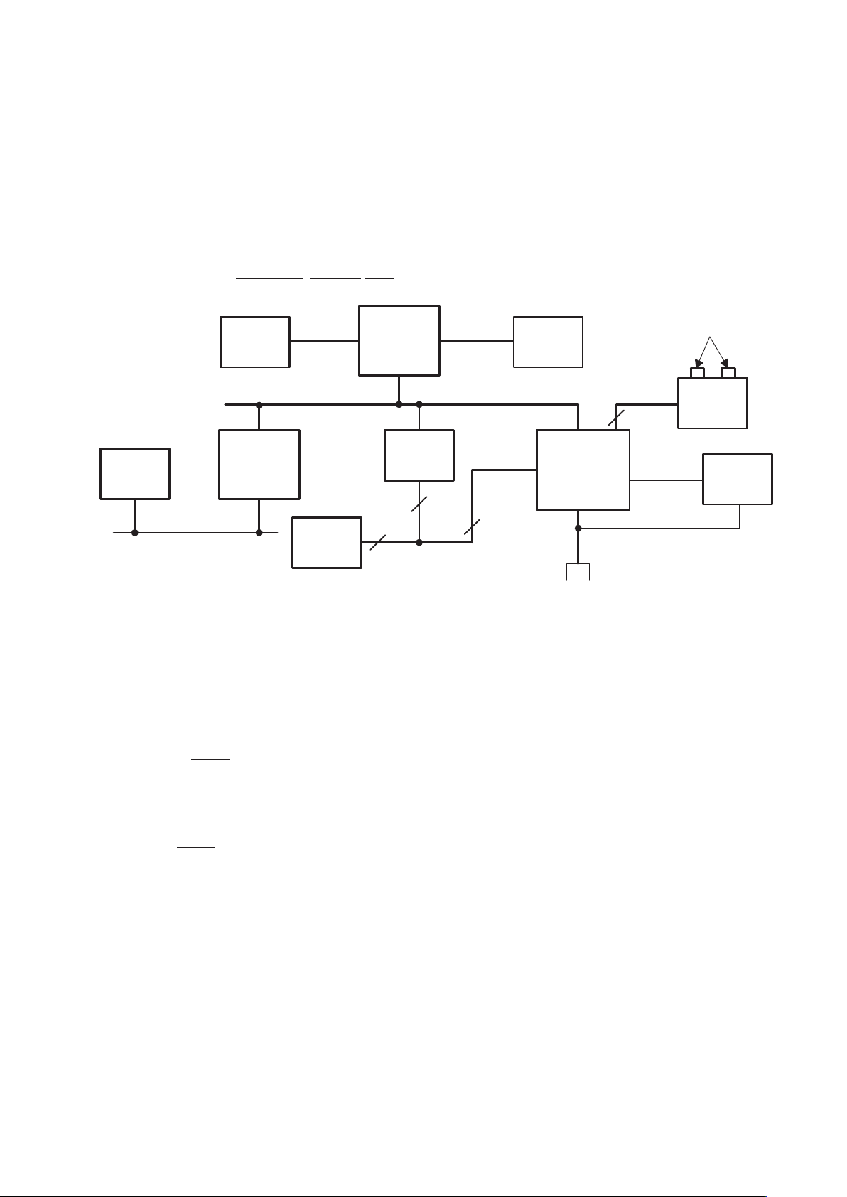
3–1
3 Feature/Protocol Descriptions
The following sections give an overview of the PCI4410. Figure 3–1 shows connections to the PCI4410. The PCI
interface includes all address/data and control signals for PCI protocol. The interrupt interface includes terminals for
parallel PCI, parallel ISA, and serialized PCI and ISA signaling. Miscellaneous system interface terminals include
multifunction terminals: SUSPEND
, RI_OUT/PME (power management control signal), and SPKROUT.
CPU
14
OHCI-PHY
Interface
1394 Ports
PCI Bus
23
PC Card Interface
Zoomed
Video
ISA
4
19
North
Bridge
Memory
1394
PHY
TPS2211
Power
Switch
PCI4410
PC Card
Controller
VGA
Controller
Audio
Codec
South
Bridge
Super
I/O
Figure 3–1. PCI4410 System Block Diagram
3.1 Power Supply Sequencing
The PCI4410 contains 3.3-V I/O buffers with 5-V tolerance requiring a core power supply and clamp voltages. The
core power supply is always 3.3 V. The clamp voltages can be either 3.3 V or 5 V, depending on the interface. The
following power-up and power-down sequences are recommended.
The power-up sequence is:
1. Apply 3.3-V power to the core.
2. Assert GRST
to the device to disable the outputs during power-up. Output drivers must be powered up in
the high-impedance state to prevent high current levels through the clamp diodes to the 5-V supply.
3. Apply the clamp voltage.
The power-down sequence is:
1. Use GRST
to switch outputs to a high-impedance state.
2. Remove the clamp voltage.
3. Remove the 3.3-V power from the core.
3.2 I/O Characteristics
Figure 3–2 shows a 3-state bidirectional buffer. Section 10.2,
Recommended Operating Conditions
, provides the
electrical characteristics of the inputs and outputs.
NOTE: The PCI4410 meets the ac specifications of the
1997 PC Card Standard
and the
PCI
Local Bus Specification.

3–2
Tied for Open Drain
OE
Pad
V
CCP
Figure 3–2. 3-State Bidirectional Buffer
NOTE: Unused pins (input or I/O) must be held high or low to prevent them from floating.
3.3 Clamping Voltages
The clamping voltages are set to match whatever external environment the PCI4410 is interfaced with: 3.3 V or 5 V.
The I/O sites can be pulled through a clamping diode to a voltage rail that protects the core from external signals.
The core power supply is always 3.3 V and is independent of the clamping voltages. For example, PCI signaling can
be either 3.3 V or 5 V, and the PCI4410 must reliably accommodate both voltage levels. This is accomplished by using
a 3.3-V I/O buffer that is 5-V tolerant, with the applicable clamping voltage applied. If a system designer desires a
5-V PCI bus, then V
CCP
can be connected to a 5-V power supply.
The PCI4410 requires four separate clamping voltages because it supports a wide range of features. The four
voltages are listed and defined in Section 10.2,
Recommended Operating Conditions
.
3.4 Peripheral Component Interconnect (PCI) Interface
The PCI4410 is fully compliant with the
PCI Local Bus Specification
. The PCI4410 provides all required signals for
PCI master or slave operation, and may operate in either a 5-V or 3.3-V signaling environment by connecting the V
CCP
terminals to the desired voltage level. In addition to the mandatory PCI signals, the PCI4410 provides the optional
interrupt signal INTA.
3.4.1 PCI Bus Lock (LOCK)
The bus-locking protocol defined in the
PCI Local Bus Specification
is not highly recommended, but is provided on
the PCI4410 as an additional compatibility feature. The PCI LOCK signal can be routed to the MFUNC4 terminal via
the multifunction routing register. See Section 4.32,
Multifunction Routing Register
, for details. Note that the use of
LOCK is only supported by PCI-to-CardBus bridges in the downstream direction (away from the processor).
PCI LOCK indicates an atomic operation that may require multiple transactions to complete. When LOCK is asserted,
nonexclusive transactions can proceed to an address that is not currently locked. A grant to start a transaction on
the PCI bus does not guarantee control of LOCK; control of LOCK is obtained under its own protocol. It is possible
for different initiators to use the PCI bus while a single master retains ownership of LOCK. Note that the CardBus
signal for this protocol is CBLOCK to avoid confusion with the bus clock.
An agent may need to do an exclusive operation because a critical access to memory might be broken into several
transactions, but the master wants exclusive rights to a region of memory. The granularity of the lock is defined by
PCI to be 16 bytes, aligned. The LOCK
protocol defined by the
PCI Local Bus Specification
allows a resource lock
without interfering with nonexclusive real-time data transfer, such as video.
The PCI bus arbiter may be designed to support only complete bus locks using the LOCK protocol. In this scenario,
the arbiter will not grant the bus to any other agent (other than the LOCK master) while LOCK is asserted. A complete
bus lock may have a significant impact on the performance of the video. The arbiter that supports complete bus lock
must grant the bus to the cache to perform a writeback due to a snoop to a modified line when a locked operation
is in progress.
The PCI4410 supports all LOCK protocol associated with PCI-to-PCI bridges, as also defined for PCI-to-CardBus
bridges. This includes disabling write posting while a locked operation is in progress, which can solve a potential

3–3
deadlock when using devices such as PCI-to-PCI bridges. The potential deadlock can occur if a CardBus target
supports delayed transactions and blocks access to the target until it completes a delayed read. This target
characteristic is prohibited by the
PCI Local Bus Specification
, and the issue is resolved by the PCI master using
LOCK.
3.4.2 Loading Subsystem Identification
The subsystem vendor ID register (see Section 4.26) and subsystem ID register (see Section 4.27) make up a
doubleword of PCI configuration space located at offset 40h for functions 0 and 1. This doubleword register is used
for system and option card (mobile dock) identification purposes and is required by some operating systems.
Implementation of this unique identifier register is a PC 99 requirement.
The PCI4410 offers two mechanisms to load a read-only value into the subsystem registers. The first mechanism
relies upon the system BIOS providing the subsystem ID value. The default access mode to the subsystem registers
is read-only, but can be made read/write by setting bit 5 (SUBSYSRW) in the system control register (see
Section 4.29) at PCI offset 80h. When this bit is set, the BIOS can write a subsystem identification value into the
registers at PCI offset 40h. The BIOS must clear the SUBSYSRW bit such that the subsystem vendor ID register and
subsystem ID register are limited to read-only access. This approach saves the added cost of implementing the serial
electrically erasable programmable ROM (EEPROM).
In some conditions, such as in a docking environment, the subsystem vendor ID register and subsystem ID register
must be loaded with a unique identifier via a serial EEPROM. The PCI4410 loads the data from the serial EEPROM
after a reset of the primary bus. Note that the SUSPEND
input gates the PCI reset from the entire PCI4410 core,
including the serial bus state machine (see Section 3.8.4,
Suspend Mode
, for details on using SUSPEND).
The PCI4410 provides a two-line serial bus host controller that can interface to a serial EEPROM. See Section 3.6,
Serial Bus Interface
, for details on the two-wire serial bus controller and applications.
3.5 PC Card Applications
This section describes the PC Card interfaces of the PCI4410:
• Card insertion/removal and recognition
• P2C power-switch interface
• Zoomed video support
• Speaker and audio applications
• LED socket activity indicators
• PC Card-16 DMA support
• PC Card controller programming model
• CardBus socket registers
3.5.1 PC Card Insertion/Removal and Recognition
The
1997 PC Card Standard
addresses the card-detection and recognition process through an interrogation
procedure that the socket must initiate on card insertion into a cold, nonpowered socket. Through this interrogation,
card voltage requirements and interface (16-bit versus CardBus) are determined.
The scheme uses the card detect and voltage sense signals. The configuration of these four terminals identifies the
card type and voltage requirements of the PC Card interface. The encoding scheme is defined in the
1997 PC Card
Standard
and in Table 3–1.

3–4
Table 3–1. PC Card Card-Detect and Voltage-Sense Connections
CD2//CCD2 CD1//CCD1 VS2//CVS2 VS1//CVS1 KEY INTERFACE VOLTAGE
Ground Ground Open Open 5 V 16-bit PC Card 5 V
Ground Ground Open Ground 5 V 16-bit PC Card 5 V and 3.3 V
Ground Ground Ground Ground 5 V 16-bit PC Card 5 V, 3.3 V, and X.X V
Ground Ground Open Ground LV 16-bit PC Card 3.3 V
Ground Connect to CVS1 Open Connect to CCD1 LV CardBus PC Card 3.3 V
Ground Ground Ground Ground LV 16-bit PC Card 3.3 V and X.X V
Connect to CVS2 Ground Connect to CCD2 Ground LV CardBus PC Card 3.3 V and X.X V
Connect to CVS1 Ground Ground Connect to CCD2 LV CardBus PC Card 3.3 V , X.X V, and Y.Y V
Ground Ground Ground Open LV 16-bit PC Card Y.Y V
Connect to CVS2 Ground Connect to CCD2 Open LV CardBus PC Card Y.Y V
Ground Connect to CVS2 Connect to CCD1 Open LV CardBus PC Card X.X V and Y.Y V
Connect to CVS1 Ground Open Connect to CCD2 LV CardBus PC Card Y.Y V
Ground Connect to CVS1 Ground Connect to CCD1 Reserved
Ground Connect to CVS2 Connect to CCD1 Ground Reserved
3.5.2 P2C Power-Switch Interface (TPS2211)
The PCI4410 provides a P2C (PCMCIA peripheral control) interface for control of the PC Card power switch. The
VCCD and VPPD terminals are used with the TI TPS221 1 single-slot PC Card power interface switch to provide power
switch support. Figure 3–3 shows terminal assignments for the TPS221 1. Figure 3–4 illustrates a typical application,
where the PCI4410 represents the PC Card controller.
VCCD0
VCCD1
3.3 V
3.3 V
5 V
5 V
GND
OC
SHDN
VPPD0
VPPD1
AVCC
AVCC
AVCC
AVPP
12 V
1
2
3
4
5
6
7
8
16
15
14
13
12
11
10
9
Figure 3–3. TPS2211 Terminal Assignments
The PCI4410 also includes support for the Maxim 1602 and Micrel MIC2562A single-channel CardBus power
switches. Application of these power switches would be similar to that of the TPS2211.
Maxim is a trademark of Maxim Integrated Products, Inc.

3–5
PCI4410
(PCMCIA
Controller)
12 V
Power Supply
V
PP1
V
PP2
V
CC
V
CC
PC Card
TPS2211
5 V
3.3 V
VCCD0
12 V
5 V
3.3 V
AVPP
AVCC
Supervisor
SHDN
SHDN
VCCD1
VPPD0
VPPD1
OC
Figure 3–4. TPS2211 Typical Application
3.5.3 Zoomed Video Support
The zoomed video (ZV) port on the PCI4410 provides an internally buffered 16-bit ZV PC Card data path. This internal
routing is programmed through the card control register (offset 91h, bits 5 and 6). Figure 3–5 summarizes the zoomed
video subsystem implemented in the PCI4410, and details the bit functions found in the card control register.
When ZV PORT_ENABLE is enabled, the zoomed video output terminals are enabled and allow the PCI4410 to route
the zoomed video data. However, no data is transmitted unless ZVENABLE (offset 91h, bit 6) is enabled. If
ZVENABLE is set to low, then the ZV output port drives a logic 0 on the PCI4410’s ZV bus.
PC Card
I/F
Card Output
Enable Logic
PC Card
Socket
ZVENABLE
ZV
PORT_ENABLE
ZVSTAT
Note: ZVSTAT must be enabled
through the GPIO Control Register
19 Video Signals
4 Audio Signals
VGA
Audio
Codec
Zoomed Video Subsystem
23
Figure 3–5. Zoomed Video Subsystem

3–6
3.5.4 Ultra Zoomed Video
Ultra zoomed video is an enhancement to the PCI4410 DMA engine and is intended to improve the 16-bit bandwidth
for MPEG I and MPEG II decoder PC Cards. This enhancement allows the PCI4410 to fetch 32 bits of data from
memory versus the 11XX/12XX 16-bit fetch capability. This enhancement allows a higher sustained throughput to
the 16-bit PC Card because the PCI4410 prefetches an extra 16 bits (32 bits total) during each PCI read transaction.
If the PCI bus becomes busy, then the PCI4410 has an extra 16 bits of data to perform back-to-back 16-bit
transactions to the PC Card before having to fetch more data. This feature is built into the DMA engine and software
is not required to enable this enhancement.
NOTE: The 11XX and 12XX series CardBus controllers have enough 16-bit bandwidth to
support MPEG II PC Card decoders. But it was decided to improve the bandwidth even more
in the 14XX series CardBus controllers.
3.5.5 D3_STAT Terminal
Additional functionality for the PCI4410 versus the 12xx series is the D3_ST AT (D3 status) pin. This pin is asserted
under the following two conditions (both conditions must be true before D3_STAT is asserted):
• Function 0 (PC Card controller) and function 1 (OHCI-Lynx) are both in D3.
• PME
is enabled for either function.
3.5.6 Internal Ring Oscillator
The internal ring oscillator provides an internal clock source for the PCI4410 so that neither the PCI clock nor an
external clock is required in order for the PCI4410 to power down a socket or interrogate a PC Card. This internal
oscillator operates nominally at 16 kHz and can be enabled by setting bit 27 (P2CCLK) of the system control register
(see Section 4.29) at PCI offset 80h to a 1. This function is disabled by default.
3.5.7 Integrated Pullup Resistors for PC Card Interface
The
1997 PC Card Standard
requires pullup resistors on various terminals to support both CardBus and 16-bit card
configurations. Unlike the PCI1210/121 1 which required external pullup resistors, the PCI4410 has integrated all of
these pullup resistors on the terminalss below, except for the CCLKRUN
/WP(IOIS16) pullup resistor.

3–7
TERMINAL NUMBER
SIGNAL NAME
PDV GHK
ADDR14/CPERR 152 F14
ADDR15/CIRDY 158 C15
ADDR19/CBLOCK 151 E19
ADDR20/CSTOP 153 E18
ADDR21/CDEVSEL 155 E17
ADDR22/CTRDY 157 A16
BVD1(STSCHG)/CSTSCHG 183 E10
BVD2(SPKR)/CAUDIO 182 C10
CD1/CCD1 123 L19
CD2/CCD2 185 A9
INPACK/CREQ 171 E12
READY/CINT 180 A10
RESET/CRST 167 F12
VS1/CVS1 179 F11
VS2/CVS2 165 E13
WAIT/CSERR 181 B10
WP(IOIS16)/CLKRUN
184†
F10
†
†
This pin requires pullup, but the PCI1451 lacks an integrated pullup
resistor.
3.5.8 SPKROUT and CAUDPWM Usage
SPKROUT carries the digital audio signal from the PC Card to the system. When a 16-bit PC Card is configured for
I/O mode, the BVD2 pin becomes SPKR. This terminal is also used in CardBus binary audio applications, and is
referred to as CAUDIO. SPKR
passes a TTL level digital audio signal to the PCI4410. The CardBus CAUDIO signal
also can pass a single-amplitude binary waveform. The binary audio signals from the PC Card socket is used in the
PCI4410 to produce SPKROUT. This output is enabled by bit 1 (SPKROUTEN) in the card control register (see
Section 4.34).
Older controllers support CAUDIO in binary or PWM mode but use the same pin (SPKROUT). Some audio chips may
not support both modes on one pin and may have a separate pin for binary and PWM. The PCI4410 implementation
includes a signal for PWM, CAUDPWM, which can be routed to a MFUNC terminal. Bit 2 (AUD2MUX) located in the
card control register is programmed to route a CardBus CAUDIO PWM terminal to CAUDPWM. See Section 4.32,
Multifunction Routing Register
, for details on configuring the MFUNC terminals.
Figure 3–6 illustrates a sample application using SPKROUT and CAUDPWM.
Speaker
Subsystem
BINARY_SPKR
System
Core Logic
PCI4410
CAUDPWM
SPKROUT
PWM_SPKR
Figure 3–6. Sample Application of SPKROUT and CAUDPWM
3.5.9 LED Socket Activity Indicators
The socket activity LEDs are provided to indicate when a PC Card is being accessed. The LED_SKT signal can be
routed to the multifunction terminals and is also provided on a dedicated pin (LED_SKT). When configured for LED

3–8
output, this terminal outputs an active high signal to indicate socket activity. See Section 4.32,
Multifunction Routing
Register
, for details on configuring the multifunction terminals.
The LED signal is active high and is driven for 64-ms durations. When the LED is not being driven high, it is driven
to a low state. Either of the two circuits shown in Figure 3–7 can be implemented to provide LED signaling. It is left
for the board designer to implement the circuit that best fits the application.
The LED activity signals are valid when a card is inserted, powered, and not in reset. For PC Card-16, the LED activity
signal is pulsed when READY/IREQ is low. For CardBus cards, the LED activity signal is pulsed if CFRAME, CIRDY,
or CREQ is active.
PCI4410
Application-
Specific Delay
Current Limiting
R ≈ 500 Ω
LED
PCI4410
Current Limiting
R ≈ 500 Ω
LED
Figure 3–7. T wo Sample LED Circuits
As indicated, the LED signals are driven for a period of 64 ms by a counter circuit. T o avoid the possibility of the LED
appearing to be stuck when the PCI clock is stopped, the LED signaling is cut off when the SUSPEND signal is
asserted, when the PCI clock is to be stopped during the clock run protocol, or when in the D2 or D1 power state.
If any additional socket activity occurs during this counter cycle, then the counter is reset and the LED signal remains
driven. If socket activity is frequent (at least once every 64 ms), then the LED signal remains driven.
3.5.10 PC Card-16 Distributed DMA Support
The PCI4410 supports a distributed DMA slave engine for 16-bit PC Card DMA support. The distributed DMA (DDMA)
slave register set provides the programmability necessary for the slave DDMA engine. T able 3–2 provides the DDMA
register configuration.
Two socket function dependent PCI configuration header registers that are critical for DDMA are the socket DMA
register 0 (see Section 4.37) and the socket DMA register 1 (see Section 4.38). Distributed DMA is enabled through
socket DMA register 0 and the contents of this register configure the PC Card-16 terminal (SPKR, IOIS16, or INP ACK)
which is used for the DMA request signal, DREQ
. The base address of the DDMA slave registers and the transfer
size (bytes or words) are programmed through the socket DMA register 1. See the programming model and register
descriptions in Section 4 for details.

3–9
Table 3–2. Distributed DMA Registers
TYPE REGISTER NAME
DDMA
BASE ADDRESS
OFFSET
R
Current address 00h
W
Reserved Page
Base address
R
Current count 04h
W
Reserved Reserved
Base count
R N/A
N/A Status 08h
W Mode
Reserved
Request Command
R Multichannel
N/A
0Ch
W Mask
Reserved
Master clear
Reserved
The DDMA registers contain control and status information consistent with the 8237 DMA controller; however, the
register locations are reordered and expanded in some cases. While the DDMA register definitions are identical to
those in the 8237 DMA controller of the same name, some register bits defined in the 8237 DMA controller do not
apply to distributed DMA in a PCI environment. In such cases, the PCI4410 implements these obsolete register bits
as read-only , nonfunctional bits. The reserved registers shown in T able 3–2 are implemented as read-only and return
0s when read. Write transactions to reserved registers have no effect.
The DDMA transfer is prefaced by several configuration steps that are specific to the PC Card and must be completed
after the PC Card is inserted and interrogated. These steps include setting the proper DREQ
signal assignment,
setting the data transfer width, and mapping and enabling the DDMA register set. As discussed above, this is done
through socket DMA register 0
and socket DMA register 1. The DMA register set is then programmed similarly to an
8237 controller, and the PCI4410 awaits a DREQ assertion from the PC Card requesting a DMA transfer.
DMA writes transfer data from the PC Card-to-PCI memory addresses. The PCI4410 accepts data 8 or 16 bits at a
time, depending on the programmed data width, and then requests access to the PCI bus by asserting its REQ signal.
Once the PCI bus is granted in an idle state, the PCI4410 initiates a PCI memory write command to the current
memory address and transfers the data in a single data phase. After terminating the PCI cycle, the PCI4410 accepts
the next byte(s) from the PC Card until the transfer count expires.
DMA reads transfer data from PCI memory addresses to the PC Card application. Upon the assertion of DREQ, the
PCI4410 asserts REQ to acquire the PCI bus. Once the bus is granted in an idle state, the PCI4410 initiates a PCI
memory read operation to the current memory address and accepts 8 or 16 bits of data, depending on the
programmed data width. After terminating the PCI cycle, the data is passed onto the PC Card. After terminating the
PC Card cycle, the PCI4410 requests access to the PCI bus again until the transfer count has expired.
The PCI4410 target interface acts normally during this procedure and accepts I/O reads and writes to the DDMA
registers. While a DDMA transfer is in progress and the host resets the DMA channel, the PCI4410 asserts TC and
ends the PC Card cycle(s). TC is indicated in the DDMA status register (see Section 7.5). At the PC Card interface,
the PCI4410 supports demand mode transfers. The PCI4410 asserts DACK during the transfer unless DREQ
is
deasserted before TC. TC is mapped to the OE PC Card terminal for DMA write operations and is mapped to the WE
PC Card terminal for DMA read operations. The DACK signal is mapped to the PC Card REG signal in all transfers,
and the DREQ
terminal is routed to one of three options which is programmed through socket DMA register 0.

3–10
3.5.11 PC Card-16 PC/PCI DMA
Some chip sets provide a way for legacy I/O devices to do DMA transfers on the PCI bus. In the PC/PCI DMA protocol,
the PCI4410 acts as a PCI target device to certain DMA related I/O addresses. The PCI4410 PCREQ and PCGNT
signals are provided as a point-to-point connection to a chipset supporting PC/PCI DMA. The PCREQ and PCGNT
signals may be routed to the MFUNC2 and MFUNC5 terminals, respectively . See Section 4.32,
Multifunction Routing
Register
, for details on configuring the multifunction terminals.
Under the PC/PCI protocol, a PCI DMA slave device (such as the PCI4410) requests a DMA transfer on a particular
channel using a serialized protocol on PCREQ
. The I/O DMA bus master arbitrates for the PCI bus and grants the
channel through a serialized protocol on PCGNT when it is ready for the transfer. The I/O cycle and memory cycles
are then presented on the PCI bus, which performs the DMA transfers similarly to legacy DMA master devices.
PC/PCI DMA is enabled for each PC Card-16 slot by setting bit 19 (CDREQEN) in the respective system control
register (see Section 4.29). On power up this bit is reset and the card PC/PCI DMA is disabled. Bit 3 (CDMA_EN)
of the system control register is a global enable for PC/PCI DMA, and is set at power up and never cleared if the
PC/PCI DMA mechanism is implemented. The desired DMA channel for each PC Card-16 slot must be configured
through bits 18–16 (CDMACHAN field) in the system control register. The channels are configured as indicated in
Table 3–3.
Table 3–3. PC/PCI Channel Assignments
SYSTEM CONTROL
REGISTER
DMA CHANNEL
CHANNEL TRANSFER
BIT 18 BIT 17 BIT16
DMA CHANNEL
DATA WIDTH
0 0 0 Channel 0 8-bit DMA transfers
0 0 1 Channel 1 8-bit DMA transfers
0 1 0 Channel 2 8-bit DMA transfers
0 1 1 Channel 3 8-bit DMA transfers
1 0 0 Channel 4 Not used
1 0 1 Channel 5 16-bit DMA transfers
1 1 0 Channel 6 16-bit DMA transfers
1 1 1 Channel 7 16-bit DMA transfers
As in distributed DMA, the PC Card terminal mapped to DREQ must be configured through socket DMA register 0
(see Section 4.37). The data transfer width is a function of channel number and the DDMA slave registers are not
used. When a DREQ
is received from a PC Card and the channel has been granted, the PCI4410 decodes the I/O
addresses listed in Table 3–4 and performs actions dependent upon the address.
T able 3–4. I/O Addresses Used for PC/PCI DMA
DMA I/O ADDRESS DMA CYCLE TYPE TERMINAL COUNT PCI CYCLE TYPE
00h Normal 0 I/O read/write
04h Normal TC 1 I/O read/write
C0h Verify 0 I/O read
C4h Verify TC 1 I/O read
When the PC/PCI DMA is used as a PC Card-16 DMA mechanism, it may not provide the performance levels of
DDMA; however, the design of a PCI target implementing PC/PCI DMA is considerably less complex. No bus master
state machine is required to support PC/PCI DMA, because the DMA control is centralized in the chipset. This DMA
scheme is often referred to as centralized DMA for this reason.
3.5.12 CardBus Socket Registers
The PCI4410 contains all registers for compatibility with the
PC Card Standard
, release 7. These registers exist as
the CardBus socket registers and are listed in Table 3–5.

3–11
T able 3–5. CardBus Socket Registers
REGISTER NAME OFFSET
Socket event 00h
Socket mask 04h
Socket present state 08h
Socket force event 0Ch
Socket control 10h
Reserved 14h
Reserved 18h
Reserved 1Ch
Socket power management 20h
3.6 Serial Bus Interface
The PCI4410 provides a serial bus interface to load subsystem identification and select register defaults through a
serial EEPROM and to provide a PC Card power switch interface alternative to P2C. See Section 3.5.2,
P2C
Power-Switch Interface (TPS2211)
, for details. The PCI4410 serial bus interface is compatible with various I2C and
SMBus components.
3.6.1 Serial Bus Interface Implementation
The PCI4410 defaults to the serial bus interface are disabled. To enable the serial interface, a pullup resistor must
be implemented on the VCCD0 and VCCD1 terminals and the appropriate pullup resistors must be implemented on
the SDA and SCL signals, that is, the MFUNC1 and MFUNC4 terminals.
The PCI4410 implements a two-pin serial interface with one clock signal (SCL) and one data signal (SDA). When
pullup resistors are provided on the VPPD0 and VPPD1 terminals, the SCL signal is mapped to the MFUNC4 terminal
and the SDA signal is mapped to the MFUNC1 terminal. The PCI4410 drives SCL at nearly 100 kHz during data
transfers, which is the maximum specified frequency for standard mode I
2
C. The serial EEPROM must be located
at address A0h. Figure 3–8 illustrates an example application implementing the two-wire serial bus.
Serial
EEPROM
PCI4410
MFUNC4
MFUNC1
SCL
SDA
V
CC
VCCD0
VCCD1
V
CC
Figure 3–8. Serial EEPROM Application
Some serial device applications may include PC Card power switches, ZV source switches, card ejectors, or other
devices that may enhance the user’s PC Card experience. The serial EEPROM device and PC Card power switches
are discussed in the sections that follow.
3.6.2 Serial Bus Interface Protocol
The SCL and SDA signals are bidirectional, open-drain signals and require pullup resistors as shown in Figure 3–8.
The PCI4410 supports up to 100 Kb/s data transfer rate and is compatible with standard mode I2C using 7-bit
addressing.
All data transfers are initiated by the serial bus master. The beginning of a data transfer is indicated by a start
condition, which is signalled when the SDA line transitions to a low state while SCL is in the high state, as illustrated

3–12
in Figure 3–9. The end of a requested data transfer is indicated by a stop condition, which is signaled by a low-to-high
transition of SDA while SCL is in the high state, as shown in Figure 3–9. Data on SDA must remain stable during the
high state of the SCL signal, as changes on the SDA signal during the high state of SCL are interpreted as control
signals, that is, a start or a stop condition.
SDA
SCL
Start
Condition
Stop
Condition
Change of
Data Allowed
Data Line Stable,
Data Valid
Figure 3–9. Serial Bus Start/Stop Conditions and Bit Transfers
Data is transferred serially in 8-bit bytes. The number of bytes that may be transmitted during a data transfer is
unlimited; however, each byte must be completed with an acknowledge bit. An acknowledge (ACK) is indicated by
the receiver pulling the SDA signal low so that it remains low during the high state of the SCL signal. Figure 3–10
illustrates the acknowledge protocol.
SCL From
Master
123 789
SDA Output
by Transmitter
SDA Output
by Receiver
Figure 3–10. Serial Bus Protocol Acknowledge
The PCI4410 is a serial bus master; all other devices connected to the serial bus external to the PCI4410 are slave
devices. As the bus master, the PCI4410 drives the SCL clock at nearly 100 kHz during bus cycles and places SCL
in a high-impedance state (zero frequency) during idle states.
Typically, the PCI4410 masters byte reads and byte writes under software control. Doubleword reads are performed
by the serial EEPROM initialization circuitry upon a PCI reset and may not be generated under software control. See
Section 3.6.3,
Serial Bus EEPROM Application
, for details on how the PCI4410 automatically loads the subsystem
identification and other register defaults through a serial bus EEPROM.
Figure 3–11 illustrates a byte write. The PCI4410 issues a start condition and sends the 7-bit slave device address
and the command bit zero. A 0 in the R/W command bit indicates that the data transfer is a write. The slave device
acknowledges if it recognizes the address. The word address byte is then sent by the PCI4410 and another slave
acknowledgment is expected. Then the PCI4410 delivers the data byte MSB first and expects a final acknowledgment
before issuing the stop condition.

3–13
Sb6 b4b5 b3 b2 b1 b0 0 b7 b6 b5 b4 b3 b2 b1 b0AA
Slave Address Word Address
R/W
S/P = Start/stop conditionA = Slave acknowledgement
b7 b6 b4b5 b3 b2 b1 b0 A P
Data Byte
Figure 3–11. Serial Bus Protocol – Byte Write
Figure 3–12 illustrates a byte read. The read protocol is very similar to the write protocol except the R/W command
bit must be set to 1 to indicate a read-data transfer. In addition, the PCI4410 master must acknowledge reception
of the read bytes from the slave transmitter. The slave transmitter drives the SDA signal during read data transfers.
The SCL signal remains driven by the PCI4410 master.
Sb6 b4b5 b3 b2 b1 b0 1 b7 b6 b5 b4 b3 b2 b1 b0A
Slave Address Word Address
R/W
S/P = Start/stop conditionA = Slave acknowledgement
A b7 b6 b4b5 b3 b2 b1 b0 M P
Data Byte
A
b7 b6 b4b5 b3 b2 b1 b0 M P
Data Byte
b6 b4b5 b3 b2 b1 b0
Slave Address
A
M = Master acknowledgement
Figure 3–12. Serial Bus Protocol – Byte Read
Figure 3–13 illustrates EEPROM interface doubleword data collection protocol.
S1 10 0 0 0 0 0 b7 b6 b5 b4 b3 b2 b1 b0AA
Slave Address Word Address
R/W
Data Byte 2 Data Byte 1 Data Byte 0 M PMM
M = Master acknowledgement
S/P = Start/stop conditionA = Slave acknowledgement
Data Byte 3 M
S1 10 00001A
Restart
R/W
Slave Address
Start
Figure 3–13. EEPROM Interface Doubleword Data Collection
3.6.3 Serial Bus EEPROM Application
When the PCI bus is reset and the serial bus interface is detected, the PCI4410 attempts to read the subsystem
identification and other register defaults from a serial EEPROM. The registers and corresponding bits that may be
loaded with defaults through the EEPROM are provided in Table 3–6.

3–14
Table 3–6. Registers and Bits Loadable Through Serial EEPROM
OHCI REGISTERS LOADED
OFFSET
REFERENCE
REGISTER REGISTER NAME BITS LOADED FROM EEPROM
0 3Eh MIN_GNT and MAX_LAT (see Section 8.14) Byte 0, bits 3–0
1 3Fh MIN_GNT and MAX_LAT (see Section 8.14) Byte 1, bits 3–0
2 PCI 2Ch Subsystem identification (see Section 8.11) Byte 0
3 PCI 2Ch Subsystem identification (see Section 8.11) Byte 1
4 PCI 2Ch Subsystem identification (see Section 8.11) Byte 2
5 PCI 2Ch Subsystem identification (see Section 8.11) Byte 3
6 PCI F4h Link enhancement control (see Section 8.21) Byte 0, bits 7, 2, 1
7 Mini-ROM address
8 PCI 24h GUID high (see Section 9.10) Byte 0
9 PCI 24h GUID high (see Section 9.10) Byte 1
10 PCI 24h GUID high (see Section 9.10) Byte 2
11 PCI 24h GUID high (see Section 9.10) Byte 3
12 PCI 28h GUID low (see Section 9.11 Byte 0
13 PCI 28h GUID low (see Section 9.11) Byte 1
14 PCI 28h GUID low (see Section 9.11) Byte 2
15 PCI 28h GUID low (see Section 9.11) Byte 3
16 Checksum
17 PCI F4h Link enhancement control (see Section 8.21) Byte 1, bits 5, 4, 1, 0
18 PCI F0h Miscellaneous configuration (see Section 8.20) Byte 0, bits 4, 2–0
19 PCI F0h Miscellaneous configuration (see Section 8.20) Byte 1, bits 7, 5, 2
CARDBUS REGISTERS LOADED
OFFSET
REFERENCE
REGISTER REGISTER NAME BITS LOADED FROM EEPROM
0 Flag byte
1 PCI 40h Subsystem vendor ID (see Section 4.26) Byte 0
2 PCI 40h Subsystem vendor ID (see Section 4.26) Byte 1
3 PCI 42h Subsystem ID (see Section 4.27) Byte 0
4 PCI 42h Subsystem ID (see Section 4.27) Byte 1
5 PCI 80h System control (see Section 4.29) Byte 0
6 PCI 80h System control (see Section 4.29) Byte 1, bits 7, 6
7 PCI 80h System control (see Section 4.29) Byte 3, bits 7, 5, 3, 2, 0
8 PCI 86h General control (see Sectin 4.31) Bits 3, 1, 0
9 PCI 8Ch Multifunction routing (see Section 4.32) Byte 0
10 PCI 8Ch Multifunction routing (see Section 4.32) Byte 1
11 PCI 8Ch Multifunction routing (see Section 4.32) Byte 2
12 PCI 8Ch Multifunction routing (see Section 4.32) Byte 3, bits 3–0
13 PCI 90h Retry status (see Section 4.33) Bits 7, 6
14 PCI 91h Card control (see Section 4.34) Bit 7
15 PCI 92h Device control (see Section 4.35) Bits 6–0
16 PCI 93h Diagnostic (see Section 4.36) Bits 7, 4–0
17 PCI A2h Power management capabilities (see Section 4.41) Bit 15
18 ExCA 00h ExCA Identification and revision (see Section 5.1) Bits 7–0

3–15
Figure 3–14 details the EEPROM data format. This format must be followed for the PCI4410 to properly load
initializations from a serial EEPROM.
Slave Address = 1010 000
Reference(0) Word Address 00h
Byte 3 (0) Word Address 01h
Byte 2 (0) Word Address 02h
Byte 1 (0) Word Address 03h
Byte 0 (0) Word Address 04h
RSVD
RSVD
RSVD
Reference(1) Word Address 08h
Reference(n) Word Address 8 × (n–1)
Byte 3 (n) Word Address 8 × (n–1) + 1
Byte 2 (n) Word Address 8 × (n–1) + 2
Byte 1 (n) Word Address 8 × (n–1) + 3
Byte 0 (n) Word Address 8 × (n–1) + 4
RSVD
RSVD
RSVD
EOL Word Address 8 × (n)
Figure 3–14. EEPROM Data Format
The byte at the EEPROM word address 00h must either contain a valid offset reference, as listed in Table 3–6, or
an end-of-list (EOL) indicator. The EOL indicator is a byte value of FFh, and indicates the end of the data to load from
the EEPROM. Only doubleword registers are loaded from the EEPROM, and all bit fields must be considered when
the EEPROM is programmed.
The serial EEPROM is addressed at slave address 1010000b by the PCI4410. All hardware address bits for the
EEPROM should be tied to the appropriate level to achieve this address. The serial EEPROM chip in the sample
application circuit (see Figure 3–8) assumes the 1010b high address nibble. The lower three address bits are terminal
inputs to the chip, and the sample application shows these terminal inputs tied to GND.
When a valid offset reference is read, four bytes are read from the EEPROM, MSB first, as illustrated in Figure 3–13.
The address autoincrements after every byte transfer according to the doubleword read protocol. Note that the word
addresses align with the data format illustrated in Figure 3–14. The PCI4410 continues to load data from the serial
EEPROM until an end-of-list indicator is read. Three reserved bytes are stuffed to maintain eight-byte data structures.
Note, the eight-byte data structure is important to provide correct addressing per the doubleword read format shown
in Figure 3–13. In addition, the reference offsets must be loaded in the EEPROM in sequential order, that is, 01h,
02h, 03h, 04h. If the offsets are not sequential, then the registers may be loaded incorrectly.
3.6.4 Accessing Serial Bus Devices Through Software
The PCI4410 provides a programming mechanism to control serial bus devices through software. The programming
is accomplished through a doubleword of PCI configuration space at offset B0h.
3.7 Programmable Interrupt Subsystem
Interrupts provide a way for I/O devices to let the microprocessor know that they require servicing. The dynamic
nature of PC Cards and the abundance of PC Card I/O applications require substantial interrupt support from the
PCI4410. The PCI4410 provides several interrupt signaling schemes to accommodate the needs of a variety of
platforms. The different mechanisms for dealing with interrupts in this device are based on various specifications and
industry standards. The ExCA register set provides interrupt control for some 16-bit PC Card functions, and the
CardBus socket register set provides interrupt control for the CardBus PC Card functions. The PCI4410 is, therefore,
backward compatible with existing interrupt control register definitions, and new registers have been defined where
required.

3–16
The PCI4410 detects PC Card interrupts and events at the PC Card interface and notifies the host controller using
one of several interrupt signaling protocols. T o simplify the discussion of interrupts in the PCI4410, PC Card interrupts
are classified as either card status change (CSC) or as functional interrupts.
The method by which any type of PCI4410 interrupt is communicated to the host interrupt controller varies from
system to system. The PCI4410 offers system designers the choice of using parallel PCI interrupt signaling, parallel
ISA-type IRQ interrupt signaling, or the IRQSER serialized ISA and/or PCI interrupt protocol. It is possible to use the
parallel PCI interrupts in combination with either parallel IRQs or serialized IRQs, as detailed in the sections that
follow. All interrupt signaling is provided through the seven multifunction terminals, MFUNC0–MFUNC6. In addition,
PCI interrupts (INTA
and INTB) are available on dedicated pins.
3.7.1 PC Card Functional and Card Status Change Interrupts
PC Card functional interrupts are defined as requests from a PC Card application for interrupt service and are
indicated by asserting specially defined signals on the PC Card interface. Functional interrupts are generated by
16-bit I/O PC Cards and by CardBus PC Cards.
Card status change (CSC)-type interrupts are defined as events at the PC Card interface that are detected by the
PCI4410 and may warrant notification of host card and socket services software for service. CSC events include both
card insertion and removal from PC Card sockets, as well as transitions of certain PC Card signals.
Table 3–7 summarizes the sources of PC Card interrupts and the type of card associated with them. CSC and
functional interrupt sources are dependent on the type of card inserted in the PC Card socket. The three types of cards
that can be inserted into any PC Card socket are:
• 16-bit memory card
• 16-bit I/O card
• CardBus cards
Table 3–7. Interrupt Mask and Flag Registers
CARD TYPE EVENT MASK FLAG
16-bit
Battery conditions
(BVD1, BVD2)
ExCA offset 05h/805h
bits 1 and 0
ExCA offset 04h/804h
bits 1 and 0
16 bit
memory
Wait states
(READY)
ExCA offset 05h/805h
bit 2
ExCA offset 04h/804h
bit 2
Change in card status
(STSCHG
)
ExCA offset 05h/805h
bit 0
ExCA offset 04h/804h
bit 0
16-bit I/O
Interrupt request
(IREQ
)
Always enabled
PCI configuration offset 91h
bit 0
All 16-bit
PC Cards
Power cycle complete
ExCA offset 05h/805h
bit 3
ExCA offset 04h/804h
bit 3
Change in card status
(CSTSCHG)
Socket mask
bit 0
Socket event
bit 0
Interrupt request
(CINT
)
Always enabled
PCI configuration offset 91h
bit 0
CardBus
Power cycle complete
Socket mask
bit 3
Socket event
bit 3
Card insertion or
removal
Socket mask
bits 2 and 1
Socket event
bits 2 and 1
Functional interrupt events are valid only for 16-bit I/O and CardBus cards; that is, the functional interrupts are not
valid for 16-bit memory cards. Furthermore, card insertion and removal-type CSC interrupts are independent of the
card type. Table 3–8 describes the PC Card interrupt events.
3–17
Table 3–8. PC Card Interrupt Events and Description
CARD TYPE EVENT TYPE SIGNAL DESCRIPTION
Battery conditions
BVD1(STSCHG)//CSTSCHG
A transition on BVD1 indicates a change in the
PC Card battery conditions.
16-bit
memory
Battery conditions
(BVD1, BVD2)
CSC
BVD2(SPKR)//CAUDIO
A transition on BVD2 indicates a change in the
PC Card battery conditions.
memory
Wait states
(READY)
CSC READY(IREQ)//CINT
A transition on READY indicates a change in the ability
of the memory PC Card to accept or provide data.
Change in card
status (STSCHG)
CSC BVD1(STSCHG)//CSTSCHG
The assertion of STSCHG indicates a status change
on the PC Card.
16-bit I/O
Interrupt request
(IREQ)
Functional READY(IREQ)//CINT
The assertion of IREQ indicates an interrupt request
from the PC Card.
Change in card
status (CSTSCHG)
CSC BVD1(STSCHG)//CSTSCHG
The assertion of CSTSCHG indicates a status change
on the PC Card.
CardBus
Interrupt request
(CINT
)
Functional READY(IREQ)//CINT
The assertion of CINT indicates an interrupt request
from the PC Card.
All PC Cards
Card insertion
or removal
CSC
CD1//CCD1,
CD2
//CCD2
A transition on either CD1//CCD1 or CD2//CCD2
indicates an insertion or removal of a 16-bit or CardBus
PC Card.
All PC Cards
Power cycle
complete
CSC N/A
An interrupt is generated when a PC Card power-up
cycle has completed.
The naming convention for PC Card signals describes the function for 16-bit memory , I/O cards, and CardBus. For
example, READY(IREQ)//CINT includes READY for 16-bit memory cards, IREQ for 16-bit I/O cards, and CINT for
CardBus cards. The 16-bit memory card signal name is first, with the I/O card signal name second, enclosed in
parentheses. The CardBus signal name follows after a forward double slash (//).
The
1997 PC Card Standard
describes the power-up sequence that must be followed by the PCI4410 when an
insertion event occurs and the host requests that the socket VCC and VPP be powered. Upon completion of this
power-up sequence, the PCI4410 interrupt scheme can be used to notify the host system (see Table 3–8), denoted
by the power cycle complete event. This interrupt source is considered a PCI4410 internal event because it depends
on the completion of applying power to the socket rather than on a signal change at the PC Card interface.
3.7.2 Interrupt Masks and Flags
Host software may individually mask (or disable) most of the potential interrupt sources listed in T able 3–8 by setting
the appropriate bits in the PCI4410. By individually masking the interrupt sources listed, software can control those
events that cause a PCI4410 interrupt. Host software has some control over the system interrupt the PCI4410 asserts
by programming the appropriate routing registers. The PCI4410 allows host software to route PC Card CSC and PC
Card functional interrupts to separate system interrupts. Interrupt routing somewhat specific to the interrupt signaling
method used is discussed in more detail in the following sections.
When an interrupt is signaled by the PCI4410, the interrupt service routine must determine which of the events listed
in T able 3–7 caused the interrupt. Internal registers in the PCI4410 provide flags that report the source of an interrupt.
By reading these status bits, the interrupt service routine can determine the action to be taken.
T able 3–7 details the registers and bits associated with masking and reporting potential interrupts. All interrupts can
be masked except the functional PC Card interrupts, and an interrupt status flag is available for all types of interrupts.
Notice that there is not a mask bit to stop the PCI4410 from passing PC Card functional interrupts through to the
appropriate interrupt scheme. These interrupts are not valid until the card is properly powered, and there should never
be a card interrupt that does not require service after proper initialization.
Table 3–7 lists the various methods of clearing the interrupt flag bits. The flag bits in the ExCA registers (16-bit PC
Card-related interrupt flags) can be cleared using two different methods. One method is an explicit write of 1 to the
flag bit to clear and the other is by reading the flag bit register. The selection of flag bit clearing is made by bit 2
(IFCMODE) in the ExCA global control register (see Section 5.22), located at ExCA offset 1Eh/5Eh/81Eh, and
defaults to the
flag cleared on read
method.

3–18
The CardBus-related interrupt flags can be cleared by an explicit write of 1 to the interrupt flag in the socket event
register (see Section 6.1). Although some of the functionality is shared between the CardBus registers and the ExCA
registers, software should not program the chip through both register sets when a CardBus card is functioning.
3.7.3 Using Parallel IRQ Interrupts
The seven multifunction terminals, MFUNC6–MFUNC0, implemented in the PCI4410 may be routed to obtain a
subset of the ISA IRQs. The IRQ choices provide ultimate flexibility in PC Card host interruptions. T o use the parallel
ISA type IRQ interrupt signaling, software must program the device control register (see Section 4.35), located at PCI
offset 92h, to select the parallel IRQ signaling scheme. See Section 4.32,
Multifunction Routing Register
, for details
on configuring the multifunction terminals.
A system using parallel IRQs requires a minimum of one PCI terminal, INT A, to signal CSC events. This requirement
is dictated by certain card and socket services software. The MFUNC pins provide (at a maximum) seven different
IRQs to support legacy 16-bit PC Card functions.
As an example, suppose the seven IRQs used by legacy PC Card applications are IRQ3, IRQ4, IRQ5, IRQ9, IRQ10,
IRQ1 1, and IRQ15. The multifunction routing register must be programmed to a value of 0x0FBA5439. This routes
the MFUNC terminals as illustrated in Figure 3–15. Not shown is that INT A must also be routed to the programmable
interrupt controller (PIC), or to some circuitry that provides parallel PCI interrupts to the host.
PCI4410 PIC
MFUNC0
MFUNC2
MFUNC3
MFUNC4
MFUNC5
MFUNC6
IRQ9
IRQ4
IRQ5
IRQ10
IRQ11
IRQ15
MFUNC1 IRQ3
Figure 3–15. IRQ Implementation
Power-on software is responsible for programming the multifunction routing register to reflect the IRQ configuration
of a system implementing the PCI4410. See Section 4.32,
Multifunction Routing Register
, for details on configuring
the multifunction terminals.
The parallel ISA type IRQ signaling from the MFUNC6–MFUNC0 terminals is compatible with those input directly into
the 8259 PIC. The parallel IRQ option is provided for system designs that require legacy ISA IRQs. Design constraints
may demand more MFUNC6–MFUNC0 IRQ terminals than the PCI4410 makes available.
3.7.4 Using Parallel PCI Interrupts
Parallel PCI interrupts are available in parallel PCI interrupt mode, parallel IRQ and parallel PCI interrupt mode, or
serialized IRQ and parallel PCI interrupt mode.
3.7.5 Using Serialized IRQSER Interrupts
The serialized interrupt protocol implemented in the PCI4410 uses a single terminal to communicate all interrupt
status information to the host controller. The protocol defines a serial packet consisting of a start cycle, multiple
interrupt indication cycles, and a stop cycle. All data in the packet is synchronous with the PCI clock. The packet data
describes 16 parallel ISA IRQ signals and the optional 4 PCI interrupts INT A, INTB, INTC, and INTD. For details on
the IRQSER protocol refer to the document
Serialized IRQ Support for PCI Systems
.

3–19
3.7.6 SMI Support in the PCI4410
The PCI4410 provides a mechanism for interrupting the system when power changes have been made to the PC
Card socket interfaces. The interrupt mechanism is designed to fit into a system maintenance interrupt (SMI) scheme.
SMI interrupts are generated by the PCI4410, when enabled, after a write cycle to either the socket control register
(see Section 6.5) of the CardBus register set or the ExCA power control register (see Section 5.3).
The SMI control is programmed through three bits in the system control register (see Section 4.29). These bits are
SMIROUTE (bit 26), SMISTATUS (bit 25), and SMIENB (bit 24). Table 3–9 describes the SMI control bits function.
Table 3–9. SMI Control
BIT NAME FUNCTION
SMIROUTE This shared bit controls whether the SMI interrupts are sent as a CSC interrupt or as IRQ2.
SMISTAT This socket-dependent bit is set when an SMI interrupt is pending. This status flag is cleared by writing back a 1.
SMIENB When set, SMI interrupt generation is enabled.
If CSC SMI interrupts are selected, then the SMI interrupt is sent as the CSC. The CSC interrupt can be either level
or edge mode, depending upon the CSCMODE bit in the ExCA global control register (see Section 5.22).
If IRQ2 is selected by SMIROUTE, then the IRQSER signaling protocol supports SMI signaling in the IRQ2 IRQ/Data
slot. In a parallel ISA IRQ system, the support for an active low IRQ2 is provided only if IRQ2 is routed to MFUNC1,
MFUNC3, or MFUNC6 through the multifunction routing register (see Section 4.32).
3.8 Power Management Overview
In addition to the low-power CMOS technology process used for the PCI4410, various features are designed into the
device to allow implementation of popular power-saving techniques. These features and techniques are discussed
in this section.
3.8.1 Clock Run Protocol
The PCI CLKRUN feature is the primary method of power management on the PCI interface of the PCI4410. CLKRUN
signaling is provided through the MFUNC6 terminal. Because some chipsets do not implement CLKRUN, this is not
always available to the system designer, and alternative power-saving features are provided. For details on the
CLKRUN protocol see the
PCI Mobile Design Guide
.
The PCI4410 does not permit the central resource to stop the PCI clock under any of the following conditions:
• Bit 1 (KEEPCLK) in the system control register (see Section 4.29) is set.
• The PC Card-16 resource manager is busy.
• The PCI4410 CardBus master state machine is busy. A cycle may be in progress on CardBus.
• The PCI4410 master is busy. There may be posted data from CardBus to PCI in the PCI4410.
• Interrupts are pending.
• The CardBus CCLK for either socket has not been stopped by the PCI4410 CCLKRUN manager.
The PCI4410 restarts the PCI clock using the CLKRUN protocol under any of the following conditions:
• A PC Card-16 IREQ or a CardBus CINT
has been asserted.
• A CardBus CBWAKE (CSTSCHG) or PC Card-16 STSCHG/RI event occurs.
• A CardBus attempts to start the CCLK using CCLKRUN.
• A CardBus card arbitrates for the CardBus bus using CREQ.
• A 16-bit DMA PC Card asserts DREQ
.
3.8.2 CardBus PC Card Power Management
The PCI4410 implements its own card power management engine that can turn off the CCLK to a socket when there
is no activity to the CardBus PC Card. The PCI clock-run protocol is followed on the CardBus CCLKRUN interface
to control this clock management.

3–20
3.8.3 16-Bit PC Card Power Management
The COE (bit 7, ExCA power control register) and PWRDWN (bit 0, ExCA global control register) bits are provided
for 16-bit PC Card power management. The COE bit places the card interface in a high-impedance state to save
power. The power savings when using this feature are minimal. The COE bit will reset the PC Card when used, and
the PWRDWN bit will not. Furthermore, the PWRDWN bit is an automatic COE; that is, the PWRDWN performs the
COE function when there is no card activity.
NOTE: The 16-bit PC Card must implement the proper pullup resistors for the COE and
PWRDWN modes.
3.8.4 Suspend Mode
The SUSPEND signal, provided for backward compatibility , gates the PRST (PCI reset) signal and the GRST (global
reset) signal from the PCI4410. Besides gating PRST and GRST, SUSPEND also gates PCLK inside the PCI4410
in order to minimize power consumption.
Gating PCLK does not create any issues with respect to the power switch interface in the PCI4410. This is because
the PCI4410 does not depend on the PCI clock to clock the power switch interface. There are two methods to clock
the power switch interface in the PCI4410:
• Use an external clock to the PCI4410 CLOCK terminal
• Use the internal oscillator
It should also be noted that asynchronous signals, such as card status change interrupts and RI_OUT , can be passed
to the host system without a PCI clock. However, if card status change interrupts are routed over the serial interrupt
stream, then the PCI clock must be restarted in order to pass the interrupt, because neither the internal oscillator nor
an external clock is routed to the serial interrupt state machine. Figure 3–16 is a functional implementation diagram.
PCI4410
Core
xRST
SUSPEND
GNT
PCLK
PCLKIN
xRSTIN
SUSPENDIN
Figure 3–16. Suspend Functional Implementation
Figure 3–17 is a signal diagram of the suspend function.

3–21
xRST
GNT
SUSPEND
PCLK
xRSTIN
SUSPENDIN
PCLKIN
External Terminals
Internal Signals
Figure 3–17. Signal Diagram of Suspend Function
3.8.5 Requirements for Suspend Mode
The suspend mode prevents the clearing of all register contents on the assertion of reset (PRST or GRST) which
would require the reconfiguration of the PCI4410 by software. Asserting the SUSPEND signal places the controller’s
PCI outputs in a high-impedance state and gates the PCLK signal internally to the controller unless a PCI transaction
is currently in process (GNT
is asserted). It is important that the PCI bus not be parked on the PCI4410 when
SUSPEND is asserted because the outputs are in a high-impedance state.
The GPIOs, MFUNC signals, and RI_OUT signals are all active during SUSPEND, unless they are disabled in the
appropriate PCI4410 registers.
3.8.6 Ring Indicate
The RI_OUT output is an important feature in power management, allowing a system to go into a suspended mode
and wake up on modem rings and other card events. TI-designed flexibility permits this signal to fit wide platform
requirements. RI_OUT on the PCI4410 can be asserted under any of the following conditions:
• A 16-bit PC Card modem in a powered socket asserts RI
to indicate to the system the presence of an
incoming call.
• A powered-down CardBus card asserts CSTSCHG (CBWAKE) requesting system and interface wake up.
• A powered CardBus card asserts CSTSCHG from the insertion/removal of cards or change in battery
voltage levels.
Figure 3–18 shows various enable bits for the PCI4410 RI_OUT function; however, it does not show the masking of
CSC events. See Table 3–7 for a detailed description of CSC interrupt masks and flags.

3–22
Card
I/F
PC Card
Socket
CSTSMASK
RIENB
RI_OUT
RI_OUT Function
RINGEN
CDRESUME
Figure 3–18. RI_OUT Functional Diagram
RI
from the 16-bit PC Card interface is masked by bit 7 (RINGEN) in the ExCA interrupt and general control register
(see Section 5.4). This is programmed on a per-socket basis and is only applicable when a 16-bit card is powered
in the socket.
The CBWAKE signaling to RI_OUT is enabled through the same mask as the CSC event for CSTSCHG. The mask
bit (bit 0, CSTSMASK) is programmed through the socket mask register (see Section 6.2) in the CardBus socket
registers.
3.8.7 PCI Power Management
The
PCI Bus Power Management Interface Specification for PCI to CardBus Bridges
establishes the infrastructure
required to let the operating system control the power of PCI functions. This is done by defining a standard PCI
interface and operations to manage the power of PCI functions on the bus. The PCI bus and the PCI functions can
be assigned one of four software-visible power management states that result in varying levels of power savings.
The four power management states of PCI functions are:
• D0 – Fully-on state
• D1 and D2 – Intermediate states
• D3 – Off state
Similarly , bus power states of the PCI bus are B0–B3. The bus power states B0–B3 are derived from the device power
state of the originating bridge device.
For the operating system (OS) to manage the device power states on the PCI bus, the PCI function should support
four power management operations. These operations are:
• Capabilities reporting
• Power status reporting
• Setting the power state
• System wake up
The OS identifies the capabilities of the PCI function by traversing the new capabilities list. The presence of
capabilities in addition to the standard PCI capabilities is indicated by a 1 in bit 4 (CAPLIST) of the status register (see
Section 4.5).
The capabilities pointer provides access to the first item in the linked list of capabilities. For the PCI4410, a CardBus
bridge with PCI configuration space header type 2, the capabilities pointer is mapped to an offset of 14h. The first
byte of each capability register block is required to be a unique ID of that capability . PCI power management has been
assigned an ID of 01h. The next byte is a pointer to the next pointer item in the list of capabilities. If there are no more
items in the list, then the next item pointer should be set to 0. The registers following the next item pointer are specific
to the function’s capability. The PCI power management capability implements the register block outlined in
Table 3–10.

3–23
Table 3–10. Power Management Registers
REGISTER NAME OFFSET
Power management capabilities Next item pointer Capability ID A0h
Data PMCSR bridge support extensions Power management control status (CSR) A4h
The power management capabilities register (see Section 4.41) is a static read-only register that provides information
on the capabilities of the function related to power management. The power management/control status register
(offset A4h, see Section 4.42) enables control of power management states and enables/monitors power
management events. The data register is an optional register that can provide dynamic data.
For more information on PCI power management, see the
PCI Bus Power Management Interface Specification for
PCI to CardBus Bridges
.
3.8.8 CardBus Bridge Power Management
The
PCI Bus Power Management Interface Specification for PCI to CardBus Bridges
was approved by PCMCIA in
December of 1997. This specification follows the device and bus state definitions provided in the
PCI Bus Power
Management Interface Specification
published by the PCI Special Interest Group (SIG). The main issue addressed
in the
PCI Bus Power Management Interface Specification for PCI to CardBus Bridges
is wake up from D3
hot
or D3
cold
without losing wake-up context (also called PME context).
The specific issues addressed by the
PCI Bus Power Management Interface Specification for PCI to CardBus Bridges
for D3 wake up are as follows:
• Preservation of device context: The specification states that a reset must occur when transitioning from D3
to D0. Some method to preserve wake-up context must be implemented so that the reset does not clear
the PME
context registers.
• Power source in D3
cold
if wake-up support is required from this state.
The Texas Instruments PCI4410 addresses these D3 wake-up issues in the following manner:
• Two resets are provided to handle preservation of PME context bits:
– Global reset (GRST
) is used only on the initial boot up of the system after power up. It places the
PCI4410 in its default state and requires BIOS to configure the device before becoming fully functional.
– PCI reset (PRST) now has dual functionality based on whether PME is enabled or not. If PME is
enabled, then PME context is preserved. If PME is not enabled, then PRST acts the same as a normal
PCI reset. Please see the master list of PME context bits in Section 3.8.10.
• Power source in D3
cold
if wake-up support is required from this state. Because VCC is removed in D3
cold
,
an auxiliary power source must be supplied to the PCI4410 VCC pins. Consult the
PCI14xx Implementation
Guide for D3 Wake-Up
or the
PCI Power Management Interface Specification for PCI to CardBus Bridges
for further information.
3.8.9 ACPI Support
The
Advanced Configuration and Power Interface (ACPI) Specification
provides a mechanism that allows unique
pieces of hardware to be described to the ACPI driver. The PCI4410 of fers a generic interface that is compliant with
ACPI design rules.
Two doublewords of general-purpose ACPI programming bits reside in PCI4410 PCI configuration space at offset
A8h. The programming model is broken into status and control functions. In compliance with ACPI, the top level event
status and enable bits reside in the general-purpose event status (see Section 4.45) and general-purpose event
enable (see Section 4.46) registers.

3–24
The status and enable bits generate an event that allows the ACPI driver to call a control method associated with the
pending status bit. The control method can then control the hardware by manipulating the hardware control bits or
by investigating child status bits and calling their respective control methods. A hierarchical implementation would
be somewhat limiting, however, as upstream devices would have to remain in some level of power state to report
events.
For more information of ACPI, see the
Advanced Configuration and Power Interface (ACPI) Specification.
3.8.10 Master List of PME Context Bits and Global Reset Only Bits
If the PME enable bit (PCI offset A4h, bit 8) is asserted, then the assertion of PRST will not clear the following PME
context bits. If the PME enable bit is not asserted, then the PME context bits are cleared with PRST . The PME context
bits are:
• Bridge control register (PCI offset 3Eh): bit 6
• Power management control/status register (PCI offset A4h): bits 15, 8
• ExCA power control register (ExCA offset 802h): bits 4, 3, 1, 0
• ExCA interrupt and general control (ExCA offset 803h): bits 6, 5
• ExCA card status change interrupt register (ExCA offset 805h): bits 3–0
• CardBus socket event register (CardBus offset 00h): bits 3–0
• CardBus socket mask register (CardBus offset 04h): bits 3–0
• CardBus socket present state register (CardBus offset 08h): bits 13–10, 7, 5–0
• CardBus socket control register (CardBus offset 10h): bits 6–4, 2–0
Global reset places all registers in their default state regardless of the state of the PME
enable bit. The GRST signal
is gated only by the SUSPEND signal. This means that assertion of SUSPEND blocks the GRST signal internally,
thus preserving all register contents. The registers cleared by GRST are:
• Subsystem ID/subsystem vendor ID (PCI offset 40h): bits 31–0
• PC Card 16-bit legacy mode base address register (PCI offset 44h): bits 31–1
• System control register (PCI offset 80h): bits 31–24, 22–14, 6–3, 1, 0
• General status register (PCI offset 85h): bits 2–0
• General control register (PCI offset 86h): bits 3, 1, 0
• Multifunction routing register (PCI offset 8Ch): bits 27–0
• Retry status register (PCI offset 90h): bits 7, 6, 3, 1
• Card control register (PCI offset 91h): bits 7–5, 2–0
• Device control register (PCI offset 92h): bits 7–0
• Diagnostic register (PCI offset 93h): bits 7–0
• Socket DMA register 0 (PCI offset 94h): bits 1–0
• Socket DMA register 1 (PCI offset 98h): bits 15–4, 2–0
• Power management capabilities register (PCI offset A2h): bit 15
• General-purpose event enable register (PCI offset AAh): bits 15, 11, 8, 4–0
• General-purpose output register (PCI offset AEh): bits 4–0
• PCI miscellaneous configuration register (OHCI function, PCI offset F0h): bits 15, 13, 10, 2–0
• Link enhancements register (OHCI function, PCI offset F4h): bits 13, 12, 9–7, 2, 1
• GPIO control register (OHCI function, PCI offset FCh): bits 29, 28, 24, 21, 20, 16, 15, 13, 12, 8, 7, 5, 4, 0
• Global unique ID low/high (OHCI function, PCI offset 24h–28h): bits 31–0
• ExCA identification and revision register (ExCA offset 00h): bits 7–0
• ExCA card status change register (ExCA offset 804h): bits 3–0
• ExCA global control register (ExCA offset 1Eh): bits 3–0

4–1
4 PC Card Controller Programming Model
This section describes the PCI4410 PCI configuration registers that make up the 256-byte PCI configuration header
for each PCI4410 function. As noted, some bits are global in nature and are accessed only through function 0.
4.1 PCI Configuration Registers (Functions 0 and 1)
The PCI4410 is a multifunction PCI device, and the PC Card controller is integrated as PCI functions 0 and 1. The
configuration header is compliant with the
PCI Local Bus Specification
as a CardBus bridge header and is PC 99
compliant as well. Table 4–1 shows the PCI configuration header, which includes both the predefined portion of the
configuration space and the user-definable registers.
Table 4–1. PCI Configuration Registers (Functions 0 and 1)
REGISTER NAME OFFSET
Device ID Vendor ID 00h
Status Command 04h
PCI class code Revision ID 08h
BIST Header type Latency timer Cache line size 0Ch
CardBus socket/ExCA base address 10h
Secondary status Reserved Capability pointer 14h
CardBus latency timer Subordinate bus number CardBus bus number PCI bus number 18h
CardBus Memory base register 0 1Ch
CardBus Memory limit register 0 20h
CardBus Memory base register 1 24h
CardBus Memory limit register 1 28h
CardBus I/O base register 0 2Ch
CardBus I/O limit register 0 30h
CardBus I/O base register 1 34h
CardBus I/O limit register 1 38h
Bridge control Interrupt pin Interrupt line 3Ch
Subsystem ID Subsystem vendor ID 40h
PC Card 16-bit I/F legacy-mode base address 44h
Reserved 48h–7Ch
System control 80h
Reserved General control General status Reserved 84h
Reserved 88h–8Bh
Multifunction routing 8Ch
Diagnostic Device control Card control Retry status 90h
Socket DMA register 0 94h
Socket DMA register 1 98h
Reserved 9Ch
Power management capabilities Next-item pointer Capability ID A0h
Power management data
Power management
control/status register
bridge support extensions
Power management control/status A4h
General-purpose event enable General-purpose event status A8h
General-purpose output General-purpose input ACh
Reserved B0h–FCh

4–2
4.2 Vendor ID Register
This 16-bit register contains a value allocated by the PCI SIG (special interest group) and identifies the manufacturer
of the PCI device. The vendor ID assigned to TI is 104Ch.
Bit 15 14 13 12 11 10 9 8 7 6 5 4 3 2 1 0
Name Vendor ID
Type R R R R R R R R R R R R R R R R
Default 0 0 0 1 0 0 0 0 0 1 0 0 1 1 0 0
Register: Vendor ID
Type: Read-only
Offset: 00h
Default: 104Ch
4.3 Device ID Register
This 16-bit register contains a value assigned to the PCI4410 by TI. The device identification for the PCI4410 is
AC41h.
Bit 15 14 13 12 11 10 9 8 7 6 5 4 3 2 1 0
Name Device ID
Type R R R R R R R R R R R R R R R R
Default 1 0 1 0 1 1 0 0 0 1 0 0 0 0 0 1
Register: Device ID
Type: Read-only
Offset: 02h
Default: AC41h

4–3
4.4 Command Register
The command register provides control over the PCI4410 interface to the PCI bus. All bit functions adhere to the
definitions in
PCI Local Bus Specification
. See Table 4–2 for the complete description of the register contents.
Bit 15 14 13 12 11 10 9 8 7 6 5 4 3 2 1 0
Name Command
Type R R R R R R R R/W R R/W R/W R R R/W R/W R/W
Default 0 0 0 0 0 0 0 0 0 0 0 0 0 0 0 0
Register: Command
Type: Read-only, Read/Write
Offset: 04h
Default: 0000h
Table 4–2. Command Register
BIT SIGNAL TYPE FUNCTION
15–10 RSVD R Reserved. Bits 15–10 return 0s when read.
9 FBB_EN R
Fast back-to-back enable. The PCI4410 does not generate fast back-to-back transactions; therefore, bit 9
returns 0 when read.
8 SERR_EN R/W
System error (SERR) enable. Bit 8 controls the enable for the SERR driver on the PCI interface. SERR can
be asserted after detecting an address parity error on the PCI bus. Both bits 8 and 6 must be set for the
PCI4410 to report address parity errors.
0 = Disable SERR
output driver (default)
1 = Enable SERR
output driver
7 STEP_EN R
Address/data stepping control. The PCI4410 does not support address/data stepping; therefore, bit 7 is
hardwired to 0.
6 PERR_EN R/W
Parity error response enable. Bit 6 controls the PCI4410’s response to parity errors through PERR. Data
parity errors are indicated by asserting PERR
, whereas address parity errors are indicated by asserting
SERR
.
0 = PCI4410 ignores detected parity error (default)
1 = PCI4410 responds to detected parity errors
5 VGA_EN R/W
VGA palette snoop. When bit 5 is set to 1, palette snooping is enabled (that is, the PCI4410 does not respond
to palette register writes and snoops the data). When bit 5 is 0, the PCI4410 treats all palette accesses like
all other accesses.
4 MWI_EN R
Memory write and invalidate enable. Bit 4 controls whether a PCI initiator device can generate memory
write-and-Invalidate commands. The PCI4410 controller does not support memory write and invalidate
commands. It uses memory write commands instead; therefore, this bit is hardwired to 0.
3 SPECIAL R
Special cycles. Bit 3 controls whether or not a PCI device ignores PCI special cycles. The PCI4410 does
not respond to special cycle operations; therefore, this bit is hardwired to 0.
2 MAST_EN R/W
Bus master control. Bit 2 controls whether or not the PCI4410 can act as a PCI bus initiator (master). The
PCI4410 can take control of the PCI bus only when this bit is set.
0 = Disables the PCI4410’s ability to generate PCI bus accesses (default)
1 = Enables the PCI4410’s ability to generate PCI bus accesses
1 MEM_EN R/W
Memory space enable. Bit 1 controls whether or not the PCI4410 can claim cycles in PCI memory space.
0 = Disables the PCI4410’s response to memory space accesses (default)
1 = Enables the PCI4410’s response to memory space accesses
0 IO_EN R/W
I/O space control. Bit 0 controls whether or not the PCI4410 can claim cycles in PCI I/O space.
0 = Disables the PCI4410 from responding to I/O space accesses (default)
1 = Enables the PCI4410 to respond to I/O space accesses

4–4
4.5 Status Register
The status register provides device information to the host system. Bits in this register may be read normally. A bit
in the status register is reset when a 1 is written to that bit location; a 0 written to a bit location has no effect. All bit
functions adhere to the definitions in the
PCI Local Bus Specification
. PCI bus status is shown through each function.
See Table 4–3 for the complete description of the register contents.
Bit 15 14 13 12 11 10 9 8 7 6 5 4 3 2 1 0
Name Status
Type R/C R/C R/C R/C R/C R R R/C R R R R R R R R
Default 0 0 0 0 0 0 1 0 0 0 0 1 0 0 0 0
Register: Status
Type: Read-only, Read/Write to Clear
Offset: 06h
Default: 0210h
Table 4–3. Status Register
BIT SIGNAL TYPE FUNCTION
15 PAR_ERR R/C Detected parity error. Bit 15 is set when a parity error is detected (either address or data).
14 SYS_ERR R/C
Signaled system error. Bit 14 is set when SERR is enabled and the PCI4410 signals a system error to the
host.
13 MABORT R/C
Received master abort. Bit 13 is set when a cycle initiated by the PCI4410 on the PCI bus has been
terminated by a master abort.
12 TABT_REC R/C
Received target abort. Bit 12 is set when a cycle initiated by the PCI4410 on the PCI bus was terminated
by a target abort.
11 TABT_SIG R/C
Signaled target abort. Bit 11 is set by the PCI4410 when it terminates a transaction on the PCI bus with a
target abort.
10–9 PCI_SPEED R
DEVSEL timing. These bits encode the timing of DEVSEL and are hardwired 01b, indicating that the
PCI4410 asserts PCI_SPEED at a medium speed on nonconfiguration cycle accesses.
8 DATAPAR R/C
Data parity error detected.
0 = The conditions for setting bit 8 have not been met.
1 = A data parity error occurred, and the following conditions were met:
a. PERR
was asserted by any PCI device including the PCI4410.
b. The PCI4410 was the bus master during the data parity error.
c. The parity error response bit is set in the command.
7 FBB_CAP R
Fast back-to-back capable. The PCI4410 cannot accept fast back-to-back transactions; therefore, bit 7 is
hardwired to 0.
6 UDF R
User-definable feature support. The PCI4410 does not support the user-definable features; therefore, bit 6
is hardwired to 0.
5 66MHZ R
66-MHz capable. The PCI4410 operates at a maximum PCLK frequency of 33 MHz; therefore, bit 5 is
hardwired to 0.
4 CAPLIST R
Capabilities list. Bit 4 returns 1 when read. This bit indicates that capabilities in addition to standard PCI
capabilities are implemented. The linked list of PCI power management capabilities is implemented in this
function.
3–0 RSVD R Reserved. Bits 3–0 return 0s when read.

4–5
4.6 Revision ID Register
The revision ID register indicates the silicon revision of the PCI4410.
Bit 7 6 5 4 3 2 1 0
Name Revision ID
Type R R R R R R R R
Default 0 0 0 0 0 0 0 1
Register: Revision ID
Type: Read-only
Offset: 08h
Default: 01h
4.7 PCI Class Code Register
The class code register recognizes the PCI4410 as a bridge device (06h) and CardBus bridge device (07h) with a
00h programming interface.
Bit 23 22 21 20 19 18 17 16 15 14 13 12 11 10 9 8 7 6 5 4 3 2 1 0
Name PCI class code
Base class Subclass Programming interface
Type R R R R R R R R R R R R R R R R R R R R R R R R
Default 0 0 0 0 0 1 1 0 0 0 0 0 0 1 1 1 0 0 0 0 0 0 0 0
Register: PCI class code
Type: Read-only
Offset: 09h
Default: 060700h
4.8 Cache Line Size Register
The cache line size register is programmed by host software to indicate the system cache line size.
Bit 7 6 5 4 3 2 1 0
Name Cache line size
Type R/W R/W R/W R/W R/W R/W R/W R/W
Default 0 0 0 0 0 0 0 0
Register: Cache line size
Type: Read/Write
Offset: 0Ch
Default: 00h

4–6
4.9 Latency Timer Register
The latency timer register specifies the latency timer for the PCI4410 in units of PCI clock cycles. When the PCI4410
is a PCI bus initiator and asserts FRAME, the latency timer begins counting from zero. If the latency timer expires
before the PCI4410 transaction has terminated, then the PCI4410 terminates the transaction when its GNT is
deasserted.
Bit 7 6 5 4 3 2 1 0
Name Latency timer
Type R/W R/W R/W R/W R/W R/W R/W R/W
Default 0 0 0 0 0 0 0 0
Register: Latency timer
Type: Read/Write
Offset: 0Dh
Default: 00h
4.10 Header Type Register
This register returns 82h when read, indicating that the PCI4410 configuration spaces adhere to the CardBus bridge
PCI header. The CardBus bridge PCI header ranges from PCI register 0 to 7Fh, and 80h–FFh are user-definable
extension registers.
Bit 7 6 5 4 3 2 1 0
Name Header type
Type R R R R R R R R
Default 1 0 0 0 0 0 1 0
Register: Header type
Type: Read-only
Offset: 0Eh
Default: 82h
4.11 BIST Register
Because the PCI4410 does not support a built-in self-test (BIST), this register returns the value of 00h when read.
Bit 7 6 5 4 3 2 1 0
Name BIST
Type R R R R R R R R
Default 0 0 0 0 0 0 0 0
Register: BIST
Type: Read-only
Offset: 0Fh
Default: 00h

4–7
4.12 CardBus Socket/ExCA Base-Address Register
The CardBus socket/ExCA base-address register is programmed with a base address referencing the CardBus
socket registers and the memory-mapped ExCA register set. Bits 31–12 are read/write and allow the base address
to be located anywhere in the 32-bit PCI memory address space on a 4-Kbyte boundary. Bits 11–0 are read-only,
returning 0s when read. When software writes all 1s to this register, the value read back is FFFF F000h, indicating
that at least 4K bytes of memory address space are required. The CardBus registers start at offset 000h, and the
memory-mapped ExCA registers begin at offset 800h.
Bit 31 30 29 28 27 26 25 24 23 22 21 20 19 18 17 16
Name CardBus socket/ExCA base-address
Type R/W R/W R/W R/W R/W R/W R/W R/W R/W R/W R/W R/W R/W R/W R/W R/W
Default 0 0 0 0 0 0 0 0 0 0 0 0 0 0 0 0
Bit 15 14 13 12 11 10 9 8 7 6 5 4 3 2 1 0
Name CardBus socket/ExCA base-address
Type R/W R/W R/W R/W R R R R R R R R R R R R
Default 0 0 0 0 0 0 0 0 0 0 0 0 0 0 0 0
Register: CardBus socket/ExCA base-address
Type: Read-only, Read/Write
Offset: 10h
Default: 0000 0000h
4.13 Capability Pointer Register
The capability pointer register provides a pointer into the PCI configuration header where the PCI power management
register block resides. PCI header doublewords at A0h and A4h provide the power management (PM) registers. The
socket has its own capability pointer register. This register returns A0h when read.
Bit 7 6 5 4 3 2 1 0
Name Capability pointer
Type R R R R R R R R
Default 1 0 1 0 0 0 0 0
Register: Capability pointer
Type: Read-only
Offset: 14h
Default: A0h

4–8
4.14 Secondary Status Register
The secondary status register is compatible with the PCI-to-PCI bridge secondary status register and indicates
CardBus-related device information to the host system. This register is very similar to the PCI status register (offset
06h); status bits are cleared by writing a 1. See Table 4–4 for a complete description of the register contents.
Bit 15 14 13 12 11 10 9 8 7 6 5 4 3 2 1 0
Name Secondary status
Type R/C R/C R/C R/C R/C R R R/C R R R R R R R R
Default 0 0 0 0 0 0 1 0 0 0 0 0 0 0 0 0
Register: Secondary status
Type: Read-only, Read/Write to Clear
Offset: 16h
Default: 0200h
Table 4–4. Secondary Status Register
BIT SIGNAL TYPE FUNCTION
15 CBPARITY R/C Detected parity error. Bit 15 is set when a CardBus parity error is detected (either address or data).
14 CBSERR R/C
Signaled system error. Bit 14 is set when CSERR is signaled by a CardBus card. The PCI4410 does not
assert CSERR
.
13 CBMABORT R/C
Received master abort. Bit 13 is set when a cycle initiated by the PCI4410 on the CardBus bus has been
terminated by a master abort.
12 REC_CBTA R/C
Received target abort. Bit 12 is set when a cycle initiated by the PCI4410 on the CardBus bus is terminated
by a target abort.
11 SIG_CBTA R/C
Signaled target abort. Bit 1 1 is set by the PCI4410 when it terminates a transaction on the CardBus bus
with a target abort.
10–9 CB_SPEED R
CDEVSEL timing. These bits encode the timing of CDEVSEL and are hardwired 01b, indicating that the
PCI4410 asserts CB_SPEED at a medium speed.
8 CB_DPAR R/C
CardBus data parity error detected.
0 = The conditions for setting bit 8 have not been met.
1 = A data parity error occurred and the following conditions were met:
a. CPERR
was asserted on the CardBus interface.
b. The PCI4410 was the bus master during the data parity error.
c. The parity error response bit is set in the bridge control.
7 CBFBB_CAP R
Fast back-to-back capable. The PCI4410 cannot accept fast back-to-back transactions; therefore, bit 7
is hardwired to 0.
6 CB_UDF R
User-definable feature support. The PCI4410 does not support the user-definable features; therefore, bit 6
is hardwired to 0.
5 CB66MHZ R
66-MHz capable. The PCI4410 CardBus interface operates at a maximum CCLK frequency of 33 MHz;
therefore, bit 5 is hardwired to 0.
4–0 RSVD R Reserved. Bits 4–0 return 0s when read.

4–9
4.15 PCI Bus Number Register
This register is programmed by the host system to indicate the bus number of the PCI bus to which the PCI4410 is
connected. The PCI4410 uses this register in conjunction with the CardBus bus number and subordinate bus number
registers to determine when to forward PCI configuration cycles to its secondary buses.
Bit 7 6 5 4 3 2 1 0
Name PCI bus number
Type R/W R/W R/W R/W R/W R/W R/W R/W
Default 0 0 0 0 0 0 0 0
Register: PCI bus number
Type: Read/Write
Offset: 18h
Default: 00h
4.16 CardBus Bus Number Register
This register is programmed by the host system to indicate the bus number of the CardBus bus to which the PCI4410
is connected. The PCI4410 uses this register in conjunction with the PCI bus number and subordinate bus number
registers to determine when to forward PCI configuration cycles to its secondary buses.
Bit 7 6 5 4 3 2 1 0
Name CardBus bus number
Type R/W R/W R/W R/W R/W R/W R/W R/W
Default 0 0 0 0 0 0 0 0
Register: CardBus bus number
Type: Read/Write
Offset: 19h
Default: 00h
4.17 Subordinate Bus Number Register
This register is programmed by the host system to indicate the highest-numbered bus below the CardBus bus. The
PCI4410 uses this register in conjunction with the PCI bus number and CardBus bus number registers to determine
when to forward PCI configuration cycles to its secondary buses.
Bit 7 6 5 4 3 2 1 0
Name Subordinate bus number
Type R/W R/W R/W R/W R/W R/W R/W R/W
Default 0 0 0 0 0 0 0 0
Register: Subordinate bus number
Type: Read/Write
Offset: 1Ah
Default: 00h

4–10
4.18 CardBus Latency Timer Register
This register is programmed by the host system to specify the latency timer for the PCI4410 CardBus interface in units
of CCLK cycles. When the PCI4410 is a CardBus initiator and asserts CFRAME, the CardBus latency timer begins
counting. If the latency timer expires before the PCI4410 transaction has terminated, then the PCI4410 terminates
the transaction at the end of the next data phase. A recommended minimum value for this register is 20h, which allows
most transactions to be completed.
Bit 7 6 5 4 3 2 1 0
Name CardBus latency timer
Type R/W R/W R/W R/W R/W R/W R/W R/W
Default 0 0 0 0 0 0 0 0
Register: CardBus latency timer
Type: Read/Write
Offset: 1Bh
Default: 00h
4.19 Memory Base Registers 0, 1
The memory base registers indicate the lower address of a PCI memory address range. These registers are used
by the PCI4410 to determine when to forward a memory transaction to the CardBus bus and when to forward a
CardBus cycle to PCI. Bits 31–12 of these registers are read/write and allow the memory base to be located anywhere
in the 32-bit PCI memory space on 4-Kbyte boundaries. Bits 11–0 are read-only and always return 0s. Write
transactions to these bits have no effect. Bits 8 and 9 of the bridge control register (see Section 4.25) specify whether
memory windows 0 and 1 are prefetchable or nonprefetchable. The memory base register or the memory limit register
must be nonzero for the PCI4410 to claim any memory transactions through CardBus memory windows (that is, these
windows are not enabled by default to pass the first 4K bytes of memory to CardBus).
Bit 31 30 29 28 27 26 25 24 23 22 21 20 19 18 17 16
Name Memory base registers 0, 1
Type R/W R/W R/W R/W R/W R/W R/W R/W R/W R/W R/W R/W R/W R/W R/W R/W
Default 0 0 0 0 0 0 0 0 0 0 0 0 0 0 0 0
Bit 15 14 13 12 11 10 9 8 7 6 5 4 3 2 1 0
Name Memory base registers 0, 1
Type R/W R/W R/W R/W R R R R R R R R R R R R
Default 0 0 0 0 0 0 0 0 0 0 0 0 0 0 0 0
Register: Memory base registers 0, 1
Type: Read-only, Read/Write
Offset: 1Ch, 24h
Default: 0000 0000h

4–11
4.20 Memory Limit Registers 0, 1
The memory limit registers indicate the upper address of a PCI memory address range. These registers are used
by the PCI4410 to determine when to forward a memory transaction to the CardBus bus and when to forward a
CardBus cycle to PCI. Bits 31–12 of these registers are read/write and allow the memory base to be located anywhere
in the 32-bit PCI memory space on 4-Kbyte boundaries. Bits 11–0 are read-only and always return 0s. Write
transactions to these bits have no effect. Bits 8 and 9 of the bridge control register specify whether memory windows
0 and 1 are prefetchable or nonprefetchable. The memory base register or the memory limit register must be nonzero
for the PCI4410 to claim any memory transactions through CardBus memory windows (that is, these windows are
not enabled by default to pass the first 4K bytes of memory to CardBus).
Bit 31 30 29 28 27 26 25 24 23 22 21 20 19 18 17 16
Name Memory limit registers 0, 1
Type R/W R/W R/W R/W R/W R/W R/W R/W R/W R/W R/W R/W R/W R/W R/W R/W
Default 0 0 0 0 0 0 0 0 0 0 0 0 0 0 0 0
Bit 15 14 13 12 11 10 9 8 7 6 5 4 3 2 1 0
Name Memory limit registers 0, 1
Type R/W R/W R/W R/W R R R R R R R R R R R R
Default 0 0 0 0 0 0 0 0 0 0 0 0 0 0 0 0
Register: Memory limit registers 0, 1
Type: Read-only, Read/Write
Offset: 20h, 28h
Default: 0000 0000h
4.21 I/O Base Registers 0, 1
The I/O base registers indicate the lower address of a PCI I/O address range. These registers are used by the
PCI4410 to determine when to forward an I/O transaction to the CardBus bus and when to forward a CardBus cycle
to the PCI bus. The lower 16 bits of this register locate the bottom of the I/O window within a 64-Kbyte page, and the
upper 16 bits (31–16) are a page register which locates this 64-Kbyte page in 32-bit PCI I/O address space. Bits 31–2
are read/write. Bits 1 and 0 are read-only and always return 0s, forcing I/O windows to be aligned on a natural
doubleword boundary.
NOTE: Either the I/O base or the I/O limit register must be nonzero to enable any I/O
transactions.
Bit 31 30 29 28 27 26 25 24 23 22 21 20 19 18 17 16
Name I/O base registers 0, 1
Type R/W R/W R/W R/W R/W R/W R/W R/W R/W R/W R/W R/W R/W R/W R/W R/W
Default 0 0 0 0 0 0 0 0 0 0 0 0 0 0 0 0
Bit 15 14 13 12 11 10 9 8 7 6 5 4 3 2 1 0
Name I/O base registers 0, 1
Type R/W R/W R/W R/W R/W R/W R/W R/W R/W R/W R/W R/W R/W R/W R R
Default 0 0 0 0 0 0 0 0 0 0 0 0 0 0 0 0
Register: I/O base registers 0, 1
Type: Read-only, Read/Write
Offset: 2Ch, 34h
Default: 0000 0000h

4–12
4.22 I/O Limit Registers 0, 1
The I/O limit registers indicate the upper address of a PCI I/O address range. These registers are used by the PCI4410
to determine when to forward an I/O transaction to the CardBus bus and when to forward a CardBus cycle to PCI.
The lower 16 bits of this register locate the top of the I/O window within a 64-Kbyte page, and the upper 16 bits are
a page register that locates this 64-Kbyte page in 32-bit PCI I/O address space. Bits 15–2 are read/write and allow
the I/O limit address to be located anywhere in the 64-Kbyte page (indicated by bits 31–16 of the appropriate I/O base)
on doubleword boundaries.
Bits 31–16 are read-only and always return 0s when read. The page is set in the I/O base register. Bits 1 and 0 are
read-only and always return 0s, forcing I/O windows to be aligned on a natural doubleword boundary. Write
transactions to read-only bits have no effect. The PCI4410 assumes that the lower 2 bits of the limit address are 1s.
NOTE: The I/O base or the I/O limit register must be nonzero to enable an I/O transaction.
Bit 31 30 29 28 27 26 25 24 23 22 21 20 19 18 17 16
Name I/O limit registers 0, 1
Type R R R R R R R R R R R R R R R R
Default 0 0 0 0 0 0 0 0 0 0 0 0 0 0 0 0
Bit 15 14 13 12 11 10 9 8 7 6 5 4 3 2 1 0
Name I/O limit registers 0, 1
Type R/W R/W R/W R/W R/W R/W R/W R/W R/W R/W R/W R/W R/W R/W R R
Default 0 0 0 0 0 0 0 0 0 0 0 0 0 0 0 0
Register: I/O limit registers 0, 1
Type: Read-only, Read/Write
Offset: 30h, 38h
Default: 0000 0000h
4.23 Interrupt Line Register
The interrupt line register communicates interrupt line routing information.
Bit 7 6 5 4 3 2 1 0
Name Interrupt line
Type R/W R/W R/W R/W R/W R/W R/W R/W
Default 1 1 1 1 1 1 1 1
Register: Interrupt line
Type: Read/Write
Offset: 3Ch
Default: FFh

4–13
4.24 Interrupt Pin Register
The value read from the interrupt pin register is function dependent and depends on the interrupt signaling mode,
selected through bits 2–1 (INTMODE field) of the device control register (see Section 4.35). The PCI4410 defaults
to serialized PCI and ISA interrupt mode.
Bit 7 6 5 4 3 2 1 0
Name Interrupt pin
Type R R R R R R R R
Default 0 0 0 0 0 0 0 1
Register: Interrupt pin
Type: Read-only
Offset: 3Dh
Default: 01h

4–14
4.25 Bridge Control Register
The bridge control register provides control over various PCI4410 bridging functions. See Table 4–5 for a complete
description of the register contents.
Bit 15 14 13 12 11 10 9 8 7 6 5 4 3 2 1 0
Name Bridge control
Type R R R R R R/W R/W R/W R/W R/W R/W R R/W R/W R/W R/W
Default 0 0 0 0 0 0 1 1 0 1 0 0 0 0 0 0
Register: Bridge control
Type: Read-only, Read/Write
Offset: 3Eh
Default: 0340h
Table 4–5. Bridge Control Register
BIT SIGNAL TYPE FUNCTION
15–11 RSVD R Reserved. Bits 15–11 return 0s when read.
10 POSTEN R/W
Write posting enable. Enables write posting to and from the CardBus sockets. Write posting enables
posting of write data on burst cycles. Operating with write posting disabled inhibits performance on burst
cycles. Note that bursted write data can be posted, but various write transactions may not.
9 PREFETCH1 R/W
Memory window 1 type. Bit 9 specifies whether or not memory window 1 is prefetchable. This bit is socket
dependent. Bit 9 is encoded as:
0 = Memory window 1 is nonprefetchable.
1 = Memory window 1 is prefetchable (default).
8 PREFETCH0 R/W
Memory window 0 type. Bit 8 specifies whether or not memory window 0 is prefetchable. This bit is
encoded as:
0 = Memory window 0 is nonprefetchable.
1 = Memory window 0 is prefetchable (default).
7 INTR R/W
PCI interrupt – IREQ routing enable. Bit 7 selects whether PC Card functional interrupts are routed to PCI
interrupts or to the IRQ specified in the ExCA registers.
0 = Functional interrupts routed to PCI interrupts (default)
1 = Functional interrupts routed to IRQ interrupts
6 CRST R/W
CardBus reset. When bit 6 is set, CRST is asserted on the CardBus interface. CRST can also be asserted
by passing a PRST
assertion to CardBus.
0 = CRST
deasserted
1 = CRST
asserted (default)
5 MABTMODE R/W
Master abort mode. Bit 5 controls how the PCI4410 responds to a master abort when the PCI4410 is an
initiator on the CardBus interface.
0 = Master aborts not signaled (default)
1 = Signal target abort on PCI. Signal SERR
(if enabled)
4 RSVD R Reserved. Bit 4 returns 0 when read.
3 VGAEN R/W
VGA enable. Bit 3 affects how the PCI4410 responds to VGA addresses. When this bit is set, accesses
to VGA addresses are forwarded.
2 ISAEN R/W
ISA mode enable. Bit 2 affects how the PCI4410 passes I/O cycles within the 64-Kbyte ISA range. This
bit is not common between sockets. When this bit is set, the PCI4410 does not forward the last 768 bytes
of each 1K I/O range to CardBus.
1 CSERREN R/W
CSERR enable. Bit 1 controls the response of the PCI4410 to CSERR signals on the CardBus bus.
0 = CSERR
is not forwarded to PCI SERR.
1 = CSERR
is forwarded to PCI SERR.
0 CPERREN R/W
CardBus parity error response enable. Bit 0 controls the response of the PCI4410 to CardBus parity errors.
0 = CardBus parity errors are ignored.
1 = CardBus parity errors are reported using CPERR
.

4–15
4.26 Subsystem Vendor ID Register
The subsystem vendor ID register is used for system and option-card identification purposes and may be required
for certain operating systems. This register is read-only or read/write, depending on the setting of bit 5 (SUBSYSRW)
in the system control register (see Section 4.29).
Bit 15 14 13 12 11 10 9 8 7 6 5 4 3 2 1 0
Name Subsystem vendor ID
Type R R R R R R R R R R R R R R R R
Default 0 0 0 0 0 0 0 0 0 0 0 0 0 0 0 0
Register: Subsystem vendor ID
Type: Read-only (Read/Write if enabled by SUBSYSRW)
Offset: 40h
Default: 0000h
4.27 Subsystem ID Register
The subsystem ID register is used for system and option-card identification purposes and may be required for certain
operating systems. This register is read-only or read/write, depending on the setting of bit 5 (SUBSYSRW) in the
system control register (see Section 4.29).
Bit 15 14 13 12 11 10 9 8 7 6 5 4 3 2 1 0
Name Subsystem ID
Type R R R R R R R R R R R R R R R R
Default 0 0 0 0 0 0 0 0 0 0 0 0 0 0 0 0
Register: Subsystem ID
Type: Read-only (Read/Write if enabled by SUBSYSRW)
Offset: 42h
Default: 0000h
4.28 PC Card 16-Bit I/F Legacy-Mode Base-Address Register
The PCI4410 supports the index/data scheme of accessing the ExCA registers, which is mapped by this register. An
address written to this register is the address for the index register and the address + 1 is the data address. Using
this access method, applications requiring index/data ExCA access can be supported. The base address can be
mapped anywhere in 32-bit I/O space on a word boundary; hence, bit 0 is read-only, returning 1 when read. See
Section 5,
ExCA Compatibility Registers
, for register offsets.
Bit 31 30 29 28 27 26 25 24 23 22 21 20 19 18 17 16
Name PC Card 16-bit I/F legacy-mode base-address
Type R/W R/W R/W R/W R/W R/W R/W R/W R/W R/W R/W R/W R/W R/W R/W R/W
Default 0 0 0 0 0 0 0 0 0 0 0 0 0 0 0 0
Bit 15 14 13 12 11 10 9 8 7 6 5 4 3 2 1 0
Name PC Card 16-bit I/F legacy-mode base-address
Type R/W R/W R/W R/W R/W R/W R/W R/W R/W R/W R/W R/W R/W R/W R/W R
Default 0 0 0 0 0 0 0 0 0 0 0 0 0 0 0 1
Register: PC Card 16-bit I/F legacy-mode base-address
Type: Read-only, Read/Write
Offset: 44h
Default: 0000 0001h

4–16
4.29 System Control Register
System-level initializations are performed through programming this doubleword register. See Table 4–6 for a
complete description of the register contents.
Bit 31 30 29 28 27 26 25 24 23 22 21 20 19 18 17 16
Name System control
Type R/W R/W R/W R/W R/W R/W R/C R/W R/W R/W R/W R/W R/W R/W R/W R/W
Default 0 0 0 0 0 0 0 0 0 1 0 0 0 1 0 0
Bit 15 14 13 12 11 10 9 8 7 6 5 4 3 2 1 0
Name System control
Type R/W R/W R R R R R R R/W R/W R/W R/W R/W R/W R/W R/W
Default 1 0 0 1 0 0 0 0 0 1 1 0 0 0 0 0
Register: System control
Type: Read-only, Read/Write, Read/Write to Clear
Offset: 80h
Default: 0044 9060h

4–17
T able 4–6. System Control Register
BIT SIGNAL TYPE FUNCTION
31–30 SER_STEP R/W
Serialized PCI interrupt routing step. Bits 31 and 30 configure the serialized PCI interrupt stream signaling
and accomplish an even distribution of interrupts signaled on the four PCI interrupt slots. Bits 31 and 30
are global to all PCI4410 functions.
00 = INTA
/INTB signal in INTA/INTB slots (default)
01 = INTA
/INTB signal in INTB/INTC slots
10 = INTA
/INTB signal in INTC/INTD slots
11 = INTA
/INTB signal in INTD/INTA slots
29 TIE_INTB_INTA R/W Tie INTB to INTA. When bit 29 is set to 1, INTB is tied to INTA (default is 0).
28 DIAGNOSTIC R/W TI diagnostic (IIC_Test) bit (default is 0).
27 OSEN R/W
Internal oscillator enable.
0 = Internal oscillator disabled (default)
1 = Internal oscillator enabled.
26 SMIROUTE R/W
SMI interrupt routing. Bit 26 selects whether IRQ2 or CSC is signaled when a write occurs to power a PC
Card socket.
0 = PC Card power change interrupts routed to IRQ2 (default)
1 = A CSC interrupt is generated on PC Card power changes.
25 SMISTATUS R/C
SMI interrupt status. This bit is set when bit 24 (SMIENB) is set and a write occurs to set the socket power.
Writing a 1 to bit 25 clears the status.
0 = SMI interrupt signaled (default)
1 = SMI interrupt not signaled
24 SMIENB R/W
SMI interrupt mode enable. When bit 24 is set and a write to the socket power control occurs, the SMI
interrupt signaling is enabled and generates an interrupt.
23 PCIPMEN R/W
PCI Bus Power Management Interface Specification
revision 1.1 enable.
0 = Use
PCI Bus Power Management Interface Specification
revision 1.0 implementation (default).
1 = Use
PCI Bus Power Management Interface Specification
revision 1.1 implementation.
Note: See power management capability register (PCI offset A2h) (Section 4.41), VERSION bits 2–0 for
additional information.
22 CBRSVD R/W
CardBus reserved terminals signaling. When a CardBus card is inserted and bit 22 is set, the RSVD
CardBus terminals are driven low. When this bit is 0, these signals are placed in a high-impedance state.
0 = 3-state CardBus RSVD
1 = Drive Cardbus RSVD low (default)
21 VCCPROT R/W
VCC protection enable.
0 = VCC protection enabled for 16-bit cards (default)
1 = VCC protection disabled for 16-bit cards
20 REDUCEZV R/W
Reduced zoomed video enable. When this bit is enabled, pins A25–A22 of the card interface for PC
Card-16 cards are placed in the high-impedance state. This bit should not be set for normal ZV operation.
This bit is encoded as:
0 = Reduced zoomed video disabled (default)
1 = Reduced zoomed video enabled
19 CDREQEN R/W
PC/PCI DMA card enable. When bit 19 is set, the PCI4410 allows 16-bit PC Cards to request PC/PCI
DMA using the DREQ
signaling. DREQ is selected through the socket DMA register 0 (see Section 4.37).
0 = Ignore DREQ
signaling from PC Cards (default)
1 = Signal DMA request on DREQ
18–16 CDMACHAN R/W
PC/PCI DMA channel assignment. Bits 18–16 are encoded as:
0–3 = 8-bit DMA channels
4 = PCI master; not used (default)
5–7 = 16-bit DMA channels
15 MRBURSTDN R/W
Memory read burst enable downstream. When bit 15 is set, memory read transactions are allowed to
burst downstream.
0 = Downstream memory read burst is disabled.
1 = Downstream memory read burst is enabled (default).

4–18
Table 4–6. System Control Register (Continued)
BIT SIGNAL TYPE FUNCTION
14 MRBURSTUP R/W
Memory read burst enable upstream. When bit 14 is set, the PCI4410 allows memory read transactions
to burst upstream.
0 = Upstream memory read burst is disabled (default).
1 = Upstream memory read burst is enabled.
13 SOCACTIVE R
Socket activity status. When set, bit 13 indicates access has been performed to or from a PC card and
is cleared upon read of this status bit.
0 = No socket activity (default)
1 = Socket activity
12 RSVD R Reserved. Bit 12 returns 1 when read.
11 PWRSTREAM R
Power stream in progress status bit. When set, bit 11 indicates that a power stream to the power switch
is in progress and a powering change has been requested. This bit is cleared when the power stream
is complete.
0 = Power stream is complete and delay has expired.
1 = Power stream is in progress.
10 DELAYUP R
Power-up delay in progress status. When set, bit 9 indicates that a power-up stream has been sent to
the power switch and proper power may not yet be stable. This bit is cleared when the power-up delay
has expired.
9 DELAYDOWN R
Power-down delay in progress status. When set, bit 10 indicates that a power-down stream has been
sent to the power switch and proper power may not yet be stable. This bit is cleared when the
power-down delay has expired.
8 INTERROGATE R
Interrogation in progress. When set, bit 8 indicates an interrogation is in progress and clears when
interrogation completes. This bit is socket dependent.
0 = Interrogation not in progress (default)
1 = Interrogation in progress
7 AUTOPWRSWEN R/W
Auto power switch enable.
0 = Bit 5 (AUTOPWRSWEN) in ExCA power control register (see Section 5.3) is disabled.
(default).
1 = Bit 5 (AUTOPWRSWEN) in ExCA power control register (see Section 5.3) is enabled.
6 PWRSAVINGS R/W
Power savings mode enable. When this bit is set, if a CB card is inserted, idle, and without a CB clock,
then the applicable CB state machine will not be clocked.
5 SUBSYSRW R/W
Subsystem ID (see Section 4.27), subsystem vendor ID (see Section 4.26), ExCA identification and
revision (see Section 5.1) registers read/write enable.
0 = Subsystem ID, subsystem vendor ID, ExCA identification and revision registers are read/write.
1 = Subsystem ID, subsystem vendor ID, ExCA identification and revision registers are read-only
(default).
4 CB_DPAR R/W
CardBus data parity error SERR signaling enable
0 = CardBus data parity error not signaled on PCI SERR
1 = CardBus data parity eror signaled on PCI SERR
3 CDMA_EN R/W
PC/PCI DMA enable. Bit 3 enables PC/PCI DMA when set if MFUNC0–MFUNC6 are configured for
centralized DMA.
0 = Centralized DMA disabled (default)
1 = Centralized DMA enabled
2 ExCAPower R/W
ExCA power control bit. Enabled by selecting the 82365SL mode.
0 = Enables 3.3 V
1 = Enables 5 V
1 KEEPCLK R/W
Keep clock. This bit works with PCI and CB CLKRUN protocols.
0 = Allows normal functioning of both CLKRUN
protocols (default)
1 = Does not allow CB clock or PCI clock to be stopped using the CLKRUN
protocols
0 RIMUX R/W
RI_OUT/PME multiplex enable.
0 = RI_OUT
and PME are both routed to the RI_OUT/PME terminal. If both are enabled at the
same time, then RI_OUT
has precedence over PME.
1 = Only PME
is routed to the RI_OUT/PME terminal.

4–19
4.30 General Status Register
The general status register provides the general device status information. The status of the serial EEPROM interface
is provided through this register. See Table 4–7 for a complete description of the register contents.
Bit 7 6 5 4 3 2 1 0
Name General status
Type R R R R R R/U R R
Default 0 0 0 0 0 X 0 0
Register: General status
Type: Read/UpdateRead-only, Read/Clear
Offset: 85h (Function 0)
Default: 00h
Table 4–7. General Status Register
BIT SIGNAL TYPE FUNCTION
7–3 RSVD R Reserved. Bits 7–3 return 0s when read.
2 EEDETECT R
Serial EEPROM detect. Serial EEPROM is detected by sampling a logic high on SCL while PRST is low.
When this bit is set, the serial ROM is detected. This status bit is encoded as:
0 = EEPROM not detected (default)
1 = EEPROM detected
1 DATAERR R/C
Serial EEPROM data error status. This bit indicates when a data error occurs on the serial EEPROM
interface. This bit may be set due to a missing acknowledge. This bit is cleared by a writeback of 1.
0 = No error detected (default)
1 = Data error detected
0 EEBUSY R
Serial EEPROM busy status. This bit indicates the status of the PCI4410 serial EEPROM circuitry. This
bit is set during the loading of the subsystem ID value.
0 = Serial EEPROM circuitry is not busy (default).
1 = Serial EEPROM circuitry is busy.
4.31 General Control Register
The general control register provides top level PCI arbitration control. See Table 4–8 for a complete description of
the register contents.
Bit 7 6 5 4 3 2 1 0
Name General control
Type R R R R R/W R R/W R/W
Default 0 0 0 0 0 0 0 0
Register: General control
Type: Read-Only, Read/Write
Offset: 86h
Default: 00h
Table 4–8. General Control Register
BIT SIGNAL TYPE FUNCTION
7–4 RSVD R Reserved. Bits 7–4 return 0s when read.
3 DISABLE_OHCI R/W When bit 3 is set, the open HCI 1394 controller function is completely nonaccessible and nonfunctional.
2 RSVD R Reserved. Bit 2 returns 0 when read.
1–0 ARB_CTRL RW
Controls top level PCI arbitration.
00 = 1394 open HCI priority
01 = CardBus priority
10 = Fair round robin
11 = Reserved (fair round robin)

4–20
4.32 Multifunction Routing Register
The multifunction routing register is used to configure the MFUNC0–MFUNC6 terminals. These terminals may be
configured for various functions. All multifunction terminals default to the general-purpose input configuration. This
register is intended to be programmed once at power-on initialization. The default value for this register may also be
loaded through a serial bus EEPROM. See Table 4–9 for a complete description of the register contents.
Bit 31 30 29 28 27 26 25 24 23 22 21 20 19 18 17 16
Name Multifunction routing
Type R R R R R/W R/W R/W R/W R/W R/W R/W R/W R/W R/W R/W R/W
Default 0 0 0 0 0 0 0 0 0 0 0 0 0 0 0 0
Bit 15 14 13 12 11 10 9 8 7 6 5 4 3 2 1 0
Name Multifunction routing
Type R/W R/W R/W R/W R/W R/W R/W R/W R/W R/W R/W R/W R/W R/W R/W R/W
Default 0 0 0 0 0 0 0 0 0 0 0 0 0 0 0 0
Register: Multifunction routing
Type: Read-only, Read/Write
Offset: 8Ch
Default: 0000 0000h
Table 4–9. Multifunction Routing Register
BIT SIGNAL TYPE FUNCTION
31–28 RSVD R Bits 31–28 return 0s when read.
27–24 MFUNC6 R/W
Multifunction terminal 6 configuration. These bits control the internal signal mapped to the MFUNC6 terminal
as follows:
0000 = RSVD 0100 = IRQ4 1000 = IRQ8 1100 = IRQ12
0001 = CLKRUN
0101 = IRQ5 1001 = IRQ9 1101 = IRQ13
0010 = IRQ2 0110 = IRQ6 1010 = IRQ10 1110 = IRQ14
0011 = IRQ3 0111 = IRQ7 1011 = IRQ11 1111 = IRQ15
23–20 MFUNC5 R/W
Multifunction terminal 5 configuration. These bits control the internal signal mapped to the MFUNC5 terminal
as follows:
0000 = GPI4 0100 = IRQ4 1000 = CAUDPWM 1100 = LED_SKT
0001 = GPO4 0101 = D3_STAT
1001 = IRQ9 1101 = Diagnostic setup: OHCI test
0010 = PCGNT
0110 = ZVSTAT 1010 = IRQ10 1110 = GPE
0011 = IRQ3 0111 = ZVSEL0 1011 = IRQ11 1111 = IRQ15
19–16 MFUNC4 R/W
Multifunction terminal 4 configuration. These bits control the internal signal mapped to the MFUNC4 terminal
as follows:
NOTE: When the serial bus mode is implemented by pulling up the VCCD0
and VCCD1 terminals, the
MFUNC4 terminal provides the SCL signaling.
0000 = GPI3 0100 = IRQ4 1000 = CAUDPWM 1100 = RI_OUT
0001 = GPO3 0101 = IRQ5 1001 = IRQ9 1101 = LED_SKT
0010 = PCI LOCK
0110 = ZVSTAT 1010 = IRQ10 1110 = GPE
0011 = IRQ3 0111 = ZVSEL0 1011 = IRQ11 1111 = IRQ15
15–12 MFUNC3 R/W
Multifunction terminal 3 configuration. These bits control the internal signal mapped to the MFUNC3 terminal
as follows:
0000 = RSVD 0100 = IRQ4 1000 = IRQ8 1100 = IRQ12
0001 = IRQSER 0101 = IRQ5 1001 = IRQ9 1101 = IRQ13
0010 = IRQ2 0110 = IRQ6 1010 = IRQ10 1110 = IRQ14
0011 = IRQ3 0111 = IRQ7 1011 = IRQ11 1111 = IRQ15
11–8 MFUNC2 R/W
Multifunction terminal 2 configuration. These bits control the internal signal mapped to the MFUNC2 terminal
as follows:
0000 = GPI2 0100 = IRQ4 1000 = CAUDPWM 1100 = RI_OUT
0001 = GPO2 0101 = IRQ5 1001 = IRQ9 1101 = D3_STAT
0010 = PCREQ 0110 = ZVSTAT 1010 = IRQ10 1110 = GPE
0011 = IRQ3 0111 = ZVSEL0 1011 = IRQ11 1111 = IRQ7

4–21
Table 4–9. Multifunction Routing Register (Continued)
BIT SIGNAL TYPE FUNCTION
7–4 MFUNC1 R/W
Multifunction terminal 1 configuration. These bits control the internal signal mapped to the MFUNC1 terminal
as follows:
NOTE: When the serial bus mode is implemented by pulling up the VCCD0
and VCCD1 terminals, the
MFUNC1 terminal provides the SDA signaling.
0000 = GPI1 0100 = IRQ4 1000 = CAUDPWM 1100 = LED_SKT
0001 = GPO1 0101 = IRQ5 1001 = IRQ9 1101 = IRQ13
0010 = D3_STAT
0110 = ZVSTAT 1010 = IRQ10 1110 = GPE
0011 = IRQ3 0111 = ZVSEL0 1011 = IRQ11 1111 = IRQ15
3–0 MFUNC0 R/W
Multifunction terminal 0 configuration. These bits control the internal signal mapped to the MFUNC0 terminal
as follows:
0000 = GPI0 0100 = IRQ4 1000 = CAUDPWM 1100 = LED_SKT
0001 = GPO0 0101 = IRQ5 1001 = IRQ9 1101 = IRQ13
0010 = INTA
0110 = ZVSTAT 1010 = IRQ10 1110 = GPE
0011 = IRQ3 0111 = ZVSEL0 1011 = IRQ11 1111 = IRQ15
4.33 Retry Status Register
The retry status register enables the retry timeout counters and displays the retry expiration status. The flags are set
when the PCI4410 retries a PCI or CardBus master request and the master does not return within 2
15
PCI clock
cycles. The flags are cleared by writing a 1 to the bit. These bits are expected to be incorporated into the PCI
command, PCI status, and bridge control registers by the PCI SIG. See Table 4–10 for a complete description of the
register contents.
Bit 7 6 5 4 3 2 1 0
Name Retry status
Type R/W R/W R R R/C R R/C R
Default 1 1 0 0 0 0 0 0
Register: Retry status
Type: Read-only, Read/Write, Read/Write to Clear
Offset: 90h
Default: C0h
Table 4–10. Retry Status Register
BIT SIGNAL TYPE FUNCTION
7 PCIRETRY R/W
PCI retry timeout counter enable. Bit 7 is encoded:
0 = PCI retry counter disabled
1 = PCI retry counter enabled (default)
6 CBRETRY R/W
CardBus retry timeout counter enable. Bit 6 is encoded:
0 = CardBus retry counter disabled
1 = CardBus retry counter enabled (default)
5–4 RSVD R Reserved. Bits 5 and 4 return 0s when read.
3 TEXP_CB R/C
CardBus target retry expired. Write a 1 to clear bit 3.
0 = Inactive (default)
1 = Retry has expired.
2 RSVD R Reserved. Bit 2 returns 0 when read.
1 TEXP_PCI R/C
PCI target retry expired. Write a 1 to clear bit 1.
0 = Inactive (default)
1 = Retry has expired.
0 RSVD R Reserved. Bit 0 returns 0 when read.
4–22
4.34 Card Control Register
The card control register is provided for PCI1130 compatibility. RI_OUT is enabled through this register. See
Table 4–11 for a complete description of the register contents.
Bit 7 6 5 4 3 2 1 0
Name Card control
Type R/W R/W R/W R R R/W R/W R/C
Default 0 0 0 0 0 0 0 0
Register: Card control
Type: Read-only, Read/Write, Read/Write to Clear
Offset: 91h
Default: 00h
Table 4–11. Card Control Register
BIT SIGNAL TYPE FUNCTION
7 RIENB R/W
Ring indicate output enable.
0 = Disables any routing of RI_OUT
signal (default)
1 = Enables RI_OUT
signal for routing to the RI_OUT/PME terminal, when bit 0 (RIMUX) in the
system control register (see Section 4.29) is set to 0, and for routing to MFUNC2 or MFUNC4.
6 ZVENABLE R/W
Compatibility ZV mode enable. When set, the PC Card socket interface ZV terminals enter a
high-impedance state. This bit defaults to 0.
5
ZV
PORT_ENABLE
R/W
ZV output port enable. When bit 5 is set, the ZV output port is enabled. If bit 6 (ZVENABLE) is set, then
ZV data from the PC Card interface is routed to the ZV output port. Otherwise, the ZV output port drives
a stable 0 pattern on all pins.
When bit 5 is not set, the ZV output port pins are placed in a high-impedance state. Default is 0.
4–3 RSVD R Reserved. Bits 4 and 3 return 0 when read.
2 AUD2MUX R/W
CardBus audio-to-IRQMUX. When set, the CAUDIO CardBus signal is routed to the corresponding
multifunction terminal which may be configured for CAUDPWM.
1 SPKROUTEN R/W
Speaker out enable. When bit 1 is set, SPKR on the PC Card is enabled and is routed to SPKROUT.
The SPKROUT terminal drives data only when the socket’s SPKROUTEN bit is set. This bit is encoded
as:
0 = SPKR
to SPKROUT not enabled (default)
1 = SPKR
to SPKROUT enabled
0 IFG R/C
Interrupt flag. Bit 0 is the interrupt flag for 16-bit I/O PC Cards and for CardBus cards. Bit 0 is set when
a functional interrupt is signaled from a PC Card interface. Write back a 1 to clear this bit.
0 = No PC Card functional interrupt detected (default)
1 = PC Card functional interrupt detected

4–23
4.35 Device Control Register
The device control register is provided for PCI1130 compatibility. The interrupt mode select and the socket-capable
force bits are programmed through this register. See Table 4–12 for a complete description of the register contents.
Bit 7 6 5 4 3 2 1 0
Name Device control
Type R/W R/W R/W R/W R/W R/W R/W R/W
Default 0 1 1 0 0 1 1 0
Register: Device control
Type: Read-only, Read/Write
Offset: 92h
Default: 66h
Table 4–12. Device Control Register
BIT SIGNAL TYPE FUNCTION
7 SKTPWR_LOCK R/W
Socket power lock bit. When this bit is set to 1, software will not be able to power down the PC Card
socket while in D3. This may be necessary to support wake on LAN or RING if the operating system
is programmed to power down a socket when the CardBus controller is placed in the D3 state.
6 3VCAPABLE R/W
3-V socket capable force
0 = Not 3-V capable
1 = 3-V capable (default)
5 IO16V2 R/W Diagnostic bit. This bit defaults to 1.
4 BUS_HOLDER_EN R/W
Bus holder cell enable/disable. Setting bit 4 to 1 enables the bus holder cells on the 1394 link
interface. Default state is 0, bus holder cells disabled.
3 TEST R/W TI test. Only a 0 should be written to bit 3.
2–1 INTMODE R/W
Interrupt signaling mode. Bits 2 and 1 select the interrupt signaling mode. The interrupt signaling
mode bits are encoded:
00 = Parallel PCI interrupts only
01 = Parallel IRQ and parallel PCI interrupts
10 = IRQ serialized interrupts and parallel PCI interrupt
11 = IRQ and PCI serialized interrupts (default)
0 RSVD R/W Reserved. Bit 0 is reserved for test purposes. Only 0 should be written to this bit.

4–24
4.36 Diagnostic Register
The diagnostic register is provided for internal TI test purposes. In additon, the diagnostic register can be used to
control CSC interrupt routing, enable asynchronous interrupts, and alter the PCI vendor ID and device ID register
fields. See Table 4–13 for a complete description of the register contents.
Bit 7 6 5 4 3 2 1 0
Name Diagnostic
Type R/W R/W R/W R/W R/W R/W R/W R/W
Default 0 0 1 0 0 0 0 1
Register: Diagnostic
Type: Read/Write
Offset: 93h
Default: 61h
Table 4–13. Diagnostic Register
BIT SIGNAL TYPE FUNCTION
7 TRUE_VAL R/W
This bit defaults to 0. Ths bit will cause software to fail to recognize the PCI4410 when set to 1. This
bit is encoded as:
0 = Reads true values from the PCI vendor ID and PCI device ID registers (default)
1 = Reads all 1s from the PCI vendor ID and PCI device ID registers
6 RSVD R/W Reserved. Bit 6 returns 0 when read.
5 CSC R/W
CSC interrupt routing control
0 = CSC interrupts routed to PCI if ExCA 803 (see Section 5.4) bit 4 = 1.
1 = CSC interrupts routed to PCI if ExCA 805 (see Section 5.6) bits 7–4 = 0000b (default).
In this case, the setting of ExCA 803 bit 4 is a don’t care.
4 DIAG4 R/W Diagnostic RETRY_DIS. Delayed transaction disabled.
3 DIAG3 R/W Diagnostic RETRY_EXT. Extends the latency from 16 to 64.
2 DIAG2 R/W Diagnostic DISCARD_TIM_SEL_CB. Set = 210, reset = 215.
1 DIAG1 R/W Diagnostic DISCARD_TIM_SEL_PCI. Set = 210, reset = 215.
0 ASYNCINT R/W
Asynchronous interrupt enable.
0 = CSC interrupt is not generated asynchronously.
1 = CSC interrupt is generated asynchronously (default).

4–25
4.37 Socket DMA Register 0
The socket DMA register 0 provides control over the PC Card DMA request (DREQ) signaling. See Table 4–14 for
a complete description of the register contents.
Bit 31 30 29 28 27 26 25 24 23 22 21 20 19 18 17 16
Name Socket DMA register 0
Type R R R R R R R R R R R R R R R R
Default 0 0 0 0 0 0 0 0 0 0 0 0 0 0 0 0
Bit 15 14 13 12 11 10 9 8 7 6 5 4 3 2 1 0
Name Socket DMA register 0
Type R R R R R R R R R R R R R R R/W R/W
Default 0 0 0 0 0 0 0 0 0 0 0 0 0 0 0 0
Register: Socket DMA register 0
Type: Read-only, Read/Write
Offset: 94h
Default: 0000 0000h
Table 4–14. Socket DMA Register 0
BIT SIGNAL TYPE FUNCTION
31–2 RSVD R Reserved. Bits 31–2 return 0s when read.
1–0 DREQPIN R/W
DMA request (DREQ). Bits 1 and 0 indicate which pin on the 16-bit PC Card interface acts as DREQ during
DMA transfers. This field is encoded as:
00 = Socket not configured for DMA (default).
01 = DREQ
uses SPKR.
10 = DREQ
uses IOIS16.
11 = DREQ
uses INPACK.

4–26
4.38 Socket DMA Register 1
The socket DMA register 1 provides control over the distributed DMA (DDMA) registers and the PCI portion of DMA
transfers. The DMA base address locates the DDMA registers in a 16-byte region within the first 64K bytes of PCI
I/O address space. See Table 4–15 for a complete description of the register contents.
NOTE: 32-bit transfers are not supported; the maximum transfer possible for 16-bit PC Cards
is 16 bits.
Bit 31 30 29 28 27 26 25 24 23 22 21 20 19 18 17 16
Name Socket DMA register 1
Type R R R R R R R R R R R R R R R R
Default 0 0 0 0 0 0 0 0 0 0 0 0 0 0 0 0
Bit 15 14 13 12 11 10 9 8 7 6 5 4 3 2 1 0
Name Socket DMA register 1
Type R/W R/W R/W R/W R/W R/W R/W R/W R/W R/W R/W R/W R R/W R/W R/W
Default 0 0 0 0 0 0 0 0 0 0 0 0 0 0 0 0
Register: Socket DMA register 1
Type: Read-only, Read/Write
Offset: 98h
Default: 0000 0000h
Table 4–15. Socket DMA Register 1
BIT SIGNAL TYPE FUNCTION
31–16 RSVD R Reserved. Bits 31–16 return 0s when read.
15–4 DMABASE R/W
DMA base address. Locates the socket’s DMA registers in PCI I/O space. This field represents a 16-bit PCI
I/O address. The upper 16 bits of the address are hardwired to 0, forcing this window to within the lower 64K
bytes of I/O address space. The lower 4 bits are hardwired to 0 and are included in the address decode.
Thus, the window is aligned to a natural 16-byte boundary.
3 EXTMODE R Extended addressing. This feature is not supported by the PCI4410 and always returns a 0.
2–1 XFERSIZE R/W
Transfer size. Bits 2 and 1 specify the width of the DMA transfer on the PC Card interface and are
encoded as:
00 = Transfers are 8 bits (default).
01 = Transfers are 16 bits.
10 = Reserved
11 = Reserved
0 DDMAEN R/W
DDMA registers decode enable. Enables the decoding of the distributed DMA registers based on the value
of bits 15–4 (DMABASE field).
0 = Disabled (default)
1 = Enabled

4–27
4.39 Capability ID Register
The capability ID register identifies the linked list item as the register for PCI power management. The register returns
01h when read, which is the unique ID assigned by the PCI SIG for the PCI location of the capabilities pointer and
the value.
Bit 7 6 5 4 3 2 1 0
Name Capability ID
Type R R R R R R R R
Default 0 0 0 0 0 0 0 1
Register: Capability ID
Type: Read-only
Offset: A0h
Default: 01h
4.40 Next-Item Pointer Register
The next-item pointer register indicates the next item in the linked list of the PCI power management capabilities.
Because the PCI4410 functions include only one capabilities item, this register returns 0s when read.
Bit 7 6 5 4 3 2 1 0
Name Next-item pointer
Type R R R R R R R R
Default 0 0 0 0 0 0 0 0
Register: Next-item pointer
Type: Read-only
Offset: A1h
Default: 00h
4–28
4.41 Power Management Capabilities Register
This register contains information on the capabilities of the PC Card function related to power management. Both
PCI4410 CardBus bridge functions support D0, D1, D2, and D3 power states. See Table 4–16 for a complete
description of the register contents.
Bit 15 14 13 12 11 10 9 8 7 6 5 4 3 2 1 0
Name Power management capabilities
Type R/W R R R R R R R R R R R R R R R
Default 1 1 1 1 1 1 1 0 0 0 1 1 0 0 0 1
Register: Power management capabilities
Type: Read/Write, Read-only
Offset: A2h
Default: FE31h
Table 4–16. Power Management Capabilities Register
BIT SIGNAL TYPE FUNCTION
PME support. This 5-bit field indicates the power states from which the PCI4410 device functions may
assert PME
. A 0 (zero) for any bit indicates that the function cannot assert the PME signal while in that
power state. These five bits return 11111b when read. Each of these bits is described below:
15 PME_SUPPORT R/W Bit 15 defaults to the value 1 indicating the PME signal can be asserted from the D3
cold
state. This bit
is R/W because wake-up support from D3
cold
is contingent on the system providing an auxiliary power
source to the VCC terminals. If the system designer chooses not to provide an auxiliary power source
to the VCC terminals for D3
cold
wake-up support, then BIOS should write a 0 to this bit.
14–11 PME_SUPPORT R Bit 14 contains the value 1, indicating that the PME signal can be asserted from D3
hot
state.
Bit 13 contains the value 1, indicating that the PME
signal can be asserted from D2 state.
Bit 12 contains the value 1, indicating that the PME
signal can be asserted from D1 state.
Bit 11 contains the value 1, indicating that the PME
signal can be asserted from the D0 state.
10 D2_SUPPORT R
D2 support. Bit 10 returns a 1 when read, indicating that the CardBus function supports the D2 device
power state.
9 D1_SUPPORT R
D1 support. Bit 9 returns a 1 when read, indicating that the CardBus function supports the D1 device
power state.
8–6 RSVD R Reserved. Bits 8–6 return 0s when read.
5 DSI R
Device-specific initialization. Bit 5 returns 1 when read, indicating that the CardBus controller function
requires special initialization (beyond the standard PCI configuration header) before the generic class
device driver is able to use it.
4 AUX_PWR R
Auxiliary power source. Bit 4 is meaningful only if bit 15 (PME_Support, D3
cold
) is set. When bit 4 is
set, it indicates that support for PME
in D3
cold
requires auxiliary power supplied by the system by way
of a proprietary delivery vehicle. When bit 4 is 0, it indicates that the function supplies its own auxiliary
power source. Because the PCI4410 requires an auxiliary power supply, this bit returns 1.
3 PMECLK R
PME clock. Bit 3 returns 0 when read, indicating that no host bus clock is required for the PCI4410 to
generate PME
.
2–0 VERSION R
Version. Bits 2–0 return 001b when read, indicating that there are four bytes of general-purpose power
management (PM) registers as described in the
PCI Bus Power Management Interface Specification
.
See system control register (PCI offset 80h) (Section 4.29), PCIPMEN bit 23, for additional information.
It is recommended that the PCIPMEN bit be set by BIOS. If PCIPMEN is set, then VERSION bits 2–0
will return 010b, indicating support for version 1.1 of the
PCI Bus Power Management Interface
Specification
.
4–29
4.42 Power Management Control/Status Register
The power management control/status register determines and changes the current power state of the PCI4410
CardBus function. The contents of this register are not affected by the internally generated reset caused by the
transition from D3
hot
to D0 state. All PCI, ExCA, and CardBus registers are reset as a result of a D3
hot
to D0 state
transition. TI-specific registers, PCI power management registers, and the legacy base address register are not reset.
See Table 4–17 for a complete description of the register contents.
Bit 15 14 13 12 11 10 9 8 7 6 5 4 3 2 1 0
Name Power management control/status
Type R/C R R R R R R R/W R R R R R R R/W R/W
Default 0 0 0 0 0 0 0 0 0 0 0 0 0 0 0 0
Register: Power management control/status
Type: Read-only, Read/Write, Read/Write to Clear
Offset: A4h
Default: 0000h
Table 4–17. Power Management Control/Status Register
BIT SIGNAL TYPE FUNCTION
15 PMESTAT R/C
PME status. Bit 15 is set when the CardBus function would normally assert PME, independent
of the state of bit 8 (PME_EN). Bit 15 is cleared by a writeback of 1, and this also clears the PME
signal if PME was asserted by this function. Writing a 0 to this bit has no effect.
14–13 DATASCALE R
Data scale. This 2-bit field returns 0s when read. The CardBus function does not return any
dynamic data as indicated by bit 4 (DYN_DATA_PME_EN).
12–9 DATASEL R
Data select. This 4-bit field returns 0s when read. The CardBus function does not return any
dynamic data as indicated by bit 4 (DYN_DATA_PME_EN).
8 PME_EN R/W
PME enable. When set to 1, bit 8 enables the function to assert PME. When reset to 0, the
assertion of PME
is disabled.
7–5 RSVD R Reserved. Bits 7–5 return 0s when read.
4 DYN_DATA_PME_EN R
Dynamic data PME enable. Bit 4 returns 0 when read because the CardBus function does not
report dymanic data.
3–2 RSVD R Reserved. Bits 3–2 return 0s when read.
1–0 PWR_STATE R/W
Power state. This 2-bit field is used both to determine the current power state of a function and
to set the function into a new power state. This field is encoded as:
00 = D0
01 = D1
10 = D2
11 = D3
hot

4–30
4.43 Power Management Control/Status Register Bridge Support Extensions
The power management control/status register bridge support extensions support PCI-bridge-specific functionality .
See Table 4–18 for a complete description of the register contents.
Bit 7 6 5 4 3 2 1 0
Name Power management control/status register bridge support extensions
Type R R/W R R R R R R
Default 1 1 0 0 0 0 0 0
Register: Power management control/status register bridge support extensions
Type: Read-only
Offset: A6h
Default: C0h
Table 4–18. Power Management Control/Status Register Bridge Support Extensions
BIT SIGNAL TYPE FUNCTION
7 BPCC_EN R
BPCC_Enable. Bus power/clock control enable. This bit returns 1 when read.
This bit is encoded as:
0 = Bus power/clock control is disabled.
1 = Bus power/clock control is enabled (default).
A 0 indicates that the bus power/clock control policies defined in the
PCI Bus Power Management
Interface Specification
are disabled. When the bus power/clock control enable mechanism is disabled,
the bridge’s power management control/status register power state field (see Section 4.42, bits 1–0)
cannot be used by the system software to control the power or the clock of the bridge’s secondary bus.
A 1 indicates that the bus power/clock control mechanism is enabled.
6 B2_B3 R/W
B2/B3 support for D3
hot
. The state of this bit determines the action that is to occur as a direct result of
programming the function to D3
hot
. This bit is only meaningful if bit 7 (BPCC_EN) is a 1. This bit is encoded
as:
0 = When the bridge is programmed to D3
hot
, its secondary bus will have its power removed (B3).
1 = When the bridge function is programmed to D3
hot
, its secondary bus’s PCI clock will be
stopped (B2). (Default)
5–0 RSVD R Reserved. Bits 5–0 return 0s when read.
4.44 Power Management Data Register
The power management data register returns 0s when read, because the CardBus functions do not report dynamic
data.
Bit 7 6 5 4 3 2 1 0
Name Power management data
Type R R R R R R R R
Default 0 0 0 0 0 0 0 0
Register: Power management data
Type: Read-only
Offset: A7h
Default: 00h

4–31
4.45 General-Purpose Event Status Register
The general-purpose event status register contains status bits that are set by different events. The bits in this register
and the corresponding GPE are cleared by writing a 1 to the corresponding bit location. See Table 4–19 for a complete
description of the register contents.
Bit 15 14 13 12 11 10 9 8 7 6 5 4 3 2 1 0
Name General-purpose event status
Type R/C R R R R/C R R R/C R R R R/C R/C R/C R/C R/C
Default 0 0 0 0 0 0 0 0 0 0 0 0 0 0 0 0
Register: General-purpose event status
Type: Read-only, Read/Write to Clear
Offset: A8h
Default: 0000h
Table 4–19. General-Purpose Event Status Register
BIT SIGNAL TYPE FUNCTION
15 ZV_STS R/C
PC card ZV status. Bit 15 is set on a change in status of bit 6 (ZVENABLE) in the card control register (see
Section 4.34).
14–12 RSVD R Reserved. Bits 14–12 return 0s when read.
11 PWR_STS R/C
Power change status. Bit 11 is set when software has changed the power state of the socket. A change
in either VCC or VPP for the socket causes this bit to be set.
10–9 RSVD R Reserved. Bits 10 and 9 return 0s when read.
8 VPP12_STS R/C
12-V VPP request status. Bit 8 is set when software has changed the requested Vpp level to or from 12 V
for the PC Card socket.
7–5 RSVD R Reserved. Bits 7–5 return 0s when read.
4 GP4_STS R/C
GPI4 Status. Bit 4 is set on a change in status of the MFUNC5 terminal input level. This bit does not depend
upon the state of a corresponding bit in the general-purpose event enable register.
3 GP3_STS R/C
GPI3 Status. Bit 3 is set on a change in status of the MFUNC4 terminal input level. This bit does not depend
upon the state of a corresponding bit in the general-purpose event enable register.
2 GP2_STS R/C
GPI2 Status. Bit 2 is set on a change in status of the MFUNC2 terminal input level. This bit does not depend
upon the state of a corresponding bit in the general-purpose event enable register.
1 GP1_STS R/C
GPI1 Status. Bit 1 is set on a change in status of the MFUNC1 terminal input level. This bit does not depend
upon the state of a corresponding bit in the general-purpose event enable register.
0 GP0_STS R/C
GPI0 Status. Bit 0 is set on a change in status of the MFUNC0 terminal input level. This bit does not depend
upon the state of a corresponding bit in the general-purpose event enable register.

4–32
4.46 General-Purpose Event Enable Register
The general-purpose event enable register contains bits that are set to enable a GPE signal. The GPE signal is driven
until the corresponding status bit is cleared and the event is serviced. The GPE can only be signaled if one of the
multifunction terminals, MFUNC6–MFUNC0, is configured for GPE signaling. See Table 4–20 for a complete
description of the register contents.
Bit 15 14 13 12 11 10 9 8 7 6 5 4 3 2 1 0
Name General-purpose event enable
Type R/W R R R R/W R R R/W R R R R/W R/W R/W R/W R/W
Default 0 0 0 0 0 0 0 0 0 0 0 0 0 0 0 0
Register: General-purpose event enable
Type: Read-only, Read/Write
Offset: AAh
Default: 0000h
T able 4–20. General-Purpose Event Enable Register
BIT SIGNAL TYPE FUNCTION
15 ZV_EN R/W
PC card socket ZV enable. When bit 15 is set, a GPE is signaled on a change in status of bit 6 (ZVENABLE)
in the card control register (see Section 4.34).
14–12 RSVD R Reserved. Bits 14–12 return 0s when read.
11 PWR_EN R/W
Power change enable. When bit 11 is set, a GPE is signaled when software has changed the power state
of the socket.
10–9 RSVD R Reserved. Bits 10 and 9 return 0s when read.
8 VPP12_EN R/W
12 V VPP request enable. When bit 8 is set, a GPE is signaled when software has changed the requested
VPP level to or from 12 V for the card socket.
7–5 RSVD R Reserved. Bits 7–5 return 0s when read.
4 GP4_EN R/W
GPI4 enable. When bit 4 is set, a GPE is signaled when there has been a change in status of the MFUNC5
terminal input level if configured as GPI4.
3 GP3_EN R/W
GPI3 enable. When bit 3 is set, a GPE is signaled when there has been a change in status of the MFUNC4
terminal input level if configured as GPI3.
2 GP2_EN R/W
GPI2 enable. When bit 2 is set, a GPE is signaled when there has been a change in status of the MFUNC2
terminal input if configured as GPI2.
1 GP1_EN R/W
GPI1 enable. When bit 1 is set, a GPE is signaled when there has been a change in status of the MFUNC1
terminal input if configured as GPI1.
0 GP0_EN R/W
GPI0 enable. When bit 0 is set, a GPE is signaled when there has been a change in status of the MFUNC0
terminal input if configured as GPI0.

4–33
4.47 General-Purpose Input Register
The general-purpose input register provides the logical value of the data input from the GPI terminals, MFUNC5,
MFUNC4, and MFUNC2–MFUNC0. See Table 4–21 for a complete description of the register contents.
Bit 15 14 13 12 11 10 9 8 7 6 5 4 3 2 1 0
Name General-purpose input
Type R R R R R R R R R R R R R R R R
Default 0 0 0 0 0 0 0 0 0 0 0 X X X X X
Register: General-purpose input
Type: Read-only
Offset: ACh
Default: 00XXh
Table 4–21. General-Purpose Input Register
BIT SIGNAL TYPE FUNCTION
15–5 RSVD R Reserved. Bits 15–5 return 0s when read.
4 GPI4_DATA R
GPI4 data bit. The value read from bit 4 represents the logical value of the data input from the MFUNC5
terminal.
3 GPI3_DATA R
GPI3 data bit. The value read from bit 3 represents the logical value of the data input from the MFUNC4
terminal.
2 GPI2_DATA R
GPI2 data bit. The value read from bit 2 represents the logical value of the data input from the MFUNC2
terminal.
1 GPI1_DATA R
GPI1 data bit. The value read from bit 1 represents the logical value of the data input from the MFUNC1
terminal.
0 GPI0_DATA R
GPI0 data bit. The value read from bit 0 represents the logical value of the data input from the MFUNC0
terminal.

4–34
4.48 General-Purpose Output Register
The general-purpose output register is used for control of the general-purpose outputs. See Table 4–22 for a
complete description of the register contents.
Bit 15 14 13 12 11 10 9 8 7 6 5 4 3 2 1 0
Name General-purpose output
Type R R R R R R R R R R R R/W R/W R/W R/W R/W
Default 0 0 0 0 0 0 0 0 0 0 0 0 0 0 0 0
Register: General-purpose output
Type: Read-only, Read/Write
Offset: AEh
Default: 0000h
Table 4–22. General-Purpose Output Register
BIT SIGNAL TYPE FUNCTION
15–5 RSVD R Reserved. Bits 15–5 return 0s when read.
4 GPO4_DATA R/W
GPO4 data bit. The value written to bit 4 represents the logical value of the data driven to the MFUNC5
terminal if configured as GPO4. Read transactions return the last data value written.
3 GPO3_DATA R/W
GPIO3 data bit. The value written to bit 3 represents the logical value of the data driven to the MFUNC4
terminal if configured as GPO3. Read transactions return the last data value written.
2 GPO2_DATA R/W
GPO2 data bit. The value written to bit 2 represents the logical value of the data driven to the MFUNC2
terminal if configured as GPO2. Read transactions return the last data value written.
1 GPO1_DATA R/W
GPO1 data bit. The value written to bit 1 represents the logical value of the data driven to the MFUNC1
terminal if configured as GPO1. Read transactions return the last data value written.
0 GPO0_DATA R/W
GPO0 data bit. The value written to bit 0 represents the logical value of the data driven to the MFUNC0
terminal if configured as GPO0. Read transactions return the last data value written.
 Loading...