


1999 PCIBus Solutions
Data Manual

Printed in U.S.A.
07/99
SCPS048

PCI2040 PCI-DSP Bridge Controller
Data Manual
Literature Number: SCPS048
July 1999
Printed on Recycled Paper

IMPORTANT NOTICE
Texas Instruments and its subsidiaries (TI) reserve the right to make changes to their products
or to discontinue any product or service without notice, and advise customers to obtain the latest
version of relevant information to verify, before placing orders, that information being relied on
is current and complete. All products are sold subject to the terms and conditions of sale supplied
at the time of order acknowledgement, including those pertaining to warranty, patent
infringement, and limitation of liability.
TI warrants performance of its semiconductor products to the specifications applicable at the
time of sale in accordance with TI’s standard warranty. Testing and other quality control
techniques are utilized to the extent TI deems necessary to support this warranty. Specific testing
of all parameters of each device is not necessarily performed, except those mandated by
government requirements.
CERTAIN APPLICATIONS USING SEMICONDUCTOR PRODUCTS MAY INVOLVE
POTENTIAL RISKS OF DEATH, PERSONAL INJURY, OR SEVERE PROPERTY OR
ENVIRONMENTAL DAMAGE (“CRITICAL APPLICATIONS”). TI SEMICONDUCTOR
PRODUCTS ARE NOT DESIGNED, AUTHORIZED, OR WARRANTED TO BE SUIT ABLE FOR
USE IN LIFE-SUPPORT DEVICES OR SYSTEMS OR OTHER CRITICAL APPLICATIONS.
INCLUSION OF TI PRODUCTS IN SUCH APPLICATIONS IS UNDERSTOOD TO BE FULLY
AT THE CUSTOMER’S RISK.
In order to minimize risks associated with the customer’s applications, adequate design and
operating safeguards must be provided by the customer to minimize inherent or procedural
hazards.
TI assumes no liability for applications assistance or customer product design. TI does not
warrant or represent that any license, either express or implied, is granted under any patent right,
copyright, mask work right, or other intellectual property right of TI covering or relating to any
combination, machine, or process in which such semiconductor products or services might be
or are used. TI’s publication of information regarding any third party’s products or services does
not constitute TI’s approval, warranty or endorsement thereof.
Copyright 1999, Texas Instruments Incorporated

iii
Contents
Section Title Page
1 Introduction 1–1. . . . . . . . . . . . . . . . . . . . . . . . . . . . . . . . . . . . . . . . . . . . . . . . . . . . . .
1.1 Description 1–1. . . . . . . . . . . . . . . . . . . . . . . . . . . . . . . . . . . . . . . . . . . . . . . . .
1.2 Features 1–1. . . . . . . . . . . . . . . . . . . . . . . . . . . . . . . . . . . . . . . . . . . . . . . . . . .
1.3 Related Documents 1–1. . . . . . . . . . . . . . . . . . . . . . . . . . . . . . . . . . . . . . . . . .
1.4 Ordering Information 1–1. . . . . . . . . . . . . . . . . . . . . . . . . . . . . . . . . . . . . . . . .
2 Terminal Descriptions 2–1. . . . . . . . . . . . . . . . . . . . . . . . . . . . . . . . . . . . . . . . . . . . .
3 PCI2040 Functional Description 3–1. . . . . . . . . . . . . . . . . . . . . . . . . . . . . . . . . . . .
3.1 PCI Interface 3–1. . . . . . . . . . . . . . . . . . . . . . . . . . . . . . . . . . . . . . . . . . . . . . . .
3.2 Accessing Internal PCI2040 Registers 3–2. . . . . . . . . . . . . . . . . . . . . . . . .
3.3 PCI_LOCK
3–2. . . . . . . . . . . . . . . . . . . . . . . . . . . . . . . . . . . . . . . . . . . . . . . . .
3.4 Serial ROM Interface 3–2. . . . . . . . . . . . . . . . . . . . . . . . . . . . . . . . . . . . . . . .
3.5 PCI2040 Host Port Interface 3–3. . . . . . . . . . . . . . . . . . . . . . . . . . . . . . . . . .
3.5.1 Identifying Implemented Ports and DSP Types 3–3. . . . . . . . . .
3.5.2 DSP Chip Selects 3–4. . . . . . . . . . . . . . . . . . . . . . . . . . . . . . . . . . .
3.5.3 HPI Register Access Control 3–4. . . . . . . . . . . . . . . . . . . . . . . . .
3.5.4 Mapping HPI DSP Memory to the Host 3–4. . . . . . . . . . . . . . . .
3.5.5 Read/Write Procedure 3–4. . . . . . . . . . . . . . . . . . . . . . . . . . . . . . .
3.5.6 HPI Interface Specific Notes 3–5. . . . . . . . . . . . . . . . . . . . . . . . .
3.6 General-Purpose I/O Interface 3–6. . . . . . . . . . . . . . . . . . . . . . . . . . . . . . . .
3.7 Interrupts 3–6. . . . . . . . . . . . . . . . . . . . . . . . . . . . . . . . . . . . . . . . . . . . . . . . . . .
3.7.1 Interrupt Event and Interrupt Mask Registers 3–6. . . . . . . . . . .
3.7.2 DSP-to-Host Interrupts 3–6. . . . . . . . . . . . . . . . . . . . . . . . . . . . . .
3.7.3 HPI Error Interrupts and HPI Error Reporting 3–7. . . . . . . . . . .
3.7.4 General-Purpose Interrupts 3–7. . . . . . . . . . . . . . . . . . . . . . . . . .
3.7.5 Interrupts Versus PME
3–7. . . . . . . . . . . . . . . . . . . . . . . . . . . . . .
3.8 PCI2040 Power Management 3–7. . . . . . . . . . . . . . . . . . . . . . . . . . . . . . . .
3.8.1 PCI Power Management Register Interface 3–8. . . . . . . . . . . .
3.8.2 PCI Power Management Device States and Transitions 3–8. .
3.9 Compact PCI Hot-Swap 3–9. . . . . . . . . . . . . . . . . . . . . . . . . . . . . . . . . . . . . .
3.10 General-Purpose Bus 3–10. . . . . . . . . . . . . . . . . . . . . . . . . . . . . . . . . . . . . . . .
3.11 Example Transactions on the General-Purpose Bus 3–11. . . . . . . . . . . . .
3.11.1 General-Purpose Bus Word Write 3–11. . . . . . . . . . . . . . . . . . . .
3.11.2 General-Purpose Bus Word Read 3–11. . . . . . . . . . . . . . . . . . . .
4 PCI2040 Programming Model 4–1. . . . . . . . . . . . . . . . . . . . . . . . . . . . . . . . . . . . . .
4.1 PCI Configuration Registers 4–1. . . . . . . . . . . . . . . . . . . . . . . . . . . . . . . . . .
4.2 Vendor and Device ID Register 4–2. . . . . . . . . . . . . . . . . . . . . . . . . . . . . . . .
4.3 PCI Command Register 4–3. . . . . . . . . . . . . . . . . . . . . . . . . . . . . . . . . . . . . .

iv
4.4 PCI Status Register 4–4. . . . . . . . . . . . . . . . . . . . . . . . . . . . . . . . . . . . . . . . . .
4.5 Revision ID 4–4. . . . . . . . . . . . . . . . . . . . . . . . . . . . . . . . . . . . . . . . . . . . . . . . .
4.6 Class Code 4–5. . . . . . . . . . . . . . . . . . . . . . . . . . . . . . . . . . . . . . . . . . . . . . . . .
4.7 Cache Line Size Register 4–5. . . . . . . . . . . . . . . . . . . . . . . . . . . . . . . . . . . . .
4.8 Latency Timer Register 4–5. . . . . . . . . . . . . . . . . . . . . . . . . . . . . . . . . . . . . . .
4.9 Header Type Register 4–6. . . . . . . . . . . . . . . . . . . . . . . . . . . . . . . . . . . . . . . .
4.10 BIST Register 4–6. . . . . . . . . . . . . . . . . . . . . . . . . . . . . . . . . . . . . . . . . . . . . . .
4.11 HPI CSR Memory Base Address Register 4–7. . . . . . . . . . . . . . . . . . . . . .
4.12 Control Space Base Address Register 4–8. . . . . . . . . . . . . . . . . . . . . . . . .
4.13 GP Bus Base Address Register 4–9. . . . . . . . . . . . . . . . . . . . . . . . . . . . . . .
4.14 Subsystem Vendor ID Register 4–9. . . . . . . . . . . . . . . . . . . . . . . . . . . . . . . .
4.15 Subsystem ID Register 4–10. . . . . . . . . . . . . . . . . . . . . . . . . . . . . . . . . . . . . . .
4.16 Capability Pointer Register 4–10. . . . . . . . . . . . . . . . . . . . . . . . . . . . . . . . . . . .
4.17 Interrupt Line Register 4–10. . . . . . . . . . . . . . . . . . . . . . . . . . . . . . . . . . . . . . .
4.18 Interrupt Pin Register 4–11. . . . . . . . . . . . . . . . . . . . . . . . . . . . . . . . . . . . . . . .
4.19 MIN_GNT Register 4–11. . . . . . . . . . . . . . . . . . . . . . . . . . . . . . . . . . . . . . . . . .
4.20 MAX_LAT Register 4–11. . . . . . . . . . . . . . . . . . . . . . . . . . . . . . . . . . . . . . . . . .
4.21 GPIO Select Register 4–12. . . . . . . . . . . . . . . . . . . . . . . . . . . . . . . . . . . . . . . .
4.22 GPIO Input Data Register 4–13. . . . . . . . . . . . . . . . . . . . . . . . . . . . . . . . . . . .
4.23 GPIO Direction Control Register 4–13. . . . . . . . . . . . . . . . . . . . . . . . . . . . . . .
4.24 GPIO Output Data Register 4–14. . . . . . . . . . . . . . . . . . . . . . . . . . . . . . . . . . .
4.25 GPIO Interrupt Event Type Register 4–14. . . . . . . . . . . . . . . . . . . . . . . . . . . .
4.26 Miscellaneous Control Register 4–15. . . . . . . . . . . . . . . . . . . . . . . . . . . . . . .
4.27 Diagnostic Register 4–16. . . . . . . . . . . . . . . . . . . . . . . . . . . . . . . . . . . . . . . . . .
4.28 PM Capability ID Register 4–16. . . . . . . . . . . . . . . . . . . . . . . . . . . . . . . . . . . .
4.29 PM Next-Item Pointer Register 4–17. . . . . . . . . . . . . . . . . . . . . . . . . . . . . . . .
4.30 Power Management Capabilities Register 4–17. . . . . . . . . . . . . . . . . . . . . .
4.31 Power Management Control/Status Register 4–18. . . . . . . . . . . . . . . . . . . .
4.32 HPI CSR I/O Base Address Register 4–19. . . . . . . . . . . . . . . . . . . . . . . . . . .
4.33 HS Capability ID Register 4–19. . . . . . . . . . . . . . . . . . . . . . . . . . . . . . . . . . . . .
4.34 HS Next-Item Pointer Register 4–20. . . . . . . . . . . . . . . . . . . . . . . . . . . . . . . .
4.35 CPCI Hot Swap Control and Status Register 4–20. . . . . . . . . . . . . . . . . . . .
5 HPI Control and Status Registers (HPI CSR) 5–1. . . . . . . . . . . . . . . . . . . . . . . .
5.1 Interrupt Event Register 5–2. . . . . . . . . . . . . . . . . . . . . . . . . . . . . . . . . . . . . .
5.2 Interrupt Mask Register 5–3. . . . . . . . . . . . . . . . . . . . . . . . . . . . . . . . . . . . . .
5.3 HPI Error Report Register 5–4. . . . . . . . . . . . . . . . . . . . . . . . . . . . . . . . . . . .
5.4 HPI Reset Register 5–4. . . . . . . . . . . . . . . . . . . . . . . . . . . . . . . . . . . . . . . . . .
5.5 HPI DSP Implementation Register 5–5. . . . . . . . . . . . . . . . . . . . . . . . . . . . .
5.6 HPI Data Width Register 5–5. . . . . . . . . . . . . . . . . . . . . . . . . . . . . . . . . . . . .
6 DSP HPI Overview 6–1. . . . . . . . . . . . . . . . . . . . . . . . . . . . . . . . . . . . . . . . . . . . . . . .
6.1 C54X Host Port Interface 6–1. . . . . . . . . . . . . . . . . . . . . . . . . . . . . . . . . . . . .
6.1.1 Modes of Operation 6–1. . . . . . . . . . . . . . . . . . . . . . . . . . . . . . . . .
6.1.2 HPI Functional Description 6–1. . . . . . . . . . . . . . . . . . . . . . . . . . .
6.1.3 HPI Registers 6–1. . . . . . . . . . . . . . . . . . . . . . . . . . . . . . . . . . . . . .

v
6.2 C54X HPI Control Register 6–3. . . . . . . . . . . . . . . . . . . . . . . . . . . . . . . . . . .
6.2.1 Auto Increment Feature 6–3. . . . . . . . . . . . . . . . . . . . . . . . . . . . .
6.2.2 Interrupts 6–3. . . . . . . . . . . . . . . . . . . . . . . . . . . . . . . . . . . . . . . . . .
6.2.3 Four Strobes (HDS1
, HDS2, HR/W, HAS) 6–4. . . . . . . . . . . . . .
6.2.4 Wait States 6–4. . . . . . . . . . . . . . . . . . . . . . . . . . . . . . . . . . . . . . . .
6.2.5 Host Read/Write Access to HPI 6–4. . . . . . . . . . . . . . . . . . . . . . .
6.2.6 HPI Memory Access During Reset 6–5. . . . . . . . . . . . . . . . . . . .
6.2.7 Examples of Transactions Targeting the C54X 6–5. . . . . . . . . .
6.2.7.1 PCI Word Write 6–5. . . . . . . . . . . . . . . . . . . . . . . . . .
6.2.7.2 PCI Word Read 6–6. . . . . . . . . . . . . . . . . . . . . . . . . .
6.2.7.3 PCI Double Word Write 6–7. . . . . . . . . . . . . . . . . . .
6.2.7.4 PCI Double Word Read 6–8. . . . . . . . . . . . . . . . . . .
6.3 C6X HPI Interface 6–8. . . . . . . . . . . . . . . . . . . . . . . . . . . . . . . . . . . . . . . . . . .
6.3.1 No SAM or HOM Modes 6–8. . . . . . . . . . . . . . . . . . . . . . . . . . . . .
6.3.2 Address/Data Bus 6–9. . . . . . . . . . . . . . . . . . . . . . . . . . . . . . . . . .
6.3.3 Byte Enables (HBE0
and HBE1) 6–9. . . . . . . . . . . . . . . . . . . . . .
6.3.4 Wait States 6–9. . . . . . . . . . . . . . . . . . . . . . . . . . . . . . . . . . . . . . . .
6.3.5 C6X HPI Registers 6–10. . . . . . . . . . . . . . . . . . . . . . . . . . . . . . . . . .
6.3.6 Software Handshaking Using HRDY and FETCH 6–11. . . . . . .
6.3.7 Host Access Sequence 6–12. . . . . . . . . . . . . . . . . . . . . . . . . . . . . .
6.3.8 Single Half-Word Cycles 6–12. . . . . . . . . . . . . . . . . . . . . . . . . . . . .
6.3.9 Memory Access Through HPI During Reset 6–12. . . . . . . . . . . .
6.3.10 Examples of Transactions Targeting the C6X 6–12. . . . . . . . . . .
7 Electrical Characteristics 7–1. . . . . . . . . . . . . . . . . . . . . . . . . . . . . . . . . . . . . . . . . .
7.1 Absolute Maximum Ratings Over Operating Temperature Ranges 7–1.
7.2 Recommended Operating Conditions 7–2. . . . . . . . . . . . . . . . . . . . . . . . . .
7.3 Electrical Characteristics Over Recommended Operating Conditions 7–3
8 Mechanical Information 8–1. . . . . . . . . . . . . . . . . . . . . . . . . . . . . . . . . . . . . . . . . . .

vi
List of Illustrations
Figure Title Page
2–1 PCI2040 Pin Diagram 2–1. . . . . . . . . . . . . . . . . . . . . . . . . . . . . . . . . . . . . . . . . . .
3–1 PCI2040 System Block Diagram 3–1. . . . . . . . . . . . . . . . . . . . . . . . . . . . . . . . . .
3–2 PCI2040 Serial ROM Data Format 3–3. . . . . . . . . . . . . . . . . . . . . . . . . . . . . . . .
3–3 PCI2040 Reset Illustration 3–9. . . . . . . . . . . . . . . . . . . . . . . . . . . . . . . . . . . . . . .
3–4 General-Purpose Bus Word Write 3–11. . . . . . . . . . . . . . . . . . . . . . . . . . . . . . . . .
3–5 General-Purpose Bus Word Read 3–12. . . . . . . . . . . . . . . . . . . . . . . . . . . . . . . . .
6–1 C54X Select Input Logic 6–4. . . . . . . . . . . . . . . . . . . . . . . . . . . . . . . . . . . . . . . . .
6–2 Word Write To HPID Without Auto-Increment Enabled 6–6. . . . . . . . . . . . . . .
6–3 Word Write From HPID Without Auto-Increment Enabled 6–7. . . . . . . . . . . .
6–4 Doubleword Write To HPID Without Auto-Increment Enabled 6–8. . . . . . . . .
6–5 Doubleword Read Trom HPID Without Auto-Increment Enabled 6–8. . . . . .
6–6 Double Word Write To HPID Without Auto-Increment Selected 6–13. . . . . . . .
6–7 Double Word Read From HPID Without Auto-Increment Selected 6–13. . . . .

vii
List of Tables
Table Title Page
2–1 Card Signal Names by GGU/PGE Pin Number 2–2. . . . . . . . . . . . . . . . . . . . .
2–2 Card Signal Names Sorted Alphabetically 2–3. . . . . . . . . . . . . . . . . . . . . . . . . .
2–3 Power Supply 2–4. . . . . . . . . . . . . . . . . . . . . . . . . . . . . . . . . . . . . . . . . . . . . . . . . .
2–4 PCI System Terminal Functions 2–5. . . . . . . . . . . . . . . . . . . . . . . . . . . . . . . . . . .
2–5 Miscellaneous Terminal Functions 2–6. . . . . . . . . . . . . . . . . . . . . . . . . . . . . . . .
2–6 Host Port Interface Terminal Functions 2–7. . . . . . . . . . . . . . . . . . . . . . . . . . . .
2–7 Compact PCI Hot Swap Interface 2–8. . . . . . . . . . . . . . . . . . . . . . . . . . . . . . . . .
2–8 General-Purpose Bus Interface 2–8. . . . . . . . . . . . . . . . . . . . . . . . . . . . . . . . . . .
3–1 PCI2040 Chip Select Decoding 3–4. . . . . . . . . . . . . . . . . . . . . . . . . . . . . . . . . . .
3–2 HPI Interface Features 3–5. . . . . . . . . . . . . . . . . . . . . . . . . . . . . . . . . . . . . . . . . .
3–3 PMC Changes for PCI PM 1.1 Register Model 3–8. . . . . . . . . . . . . . . . . . . . . .
3–4 General-Purpose Bus Signals 3–10. . . . . . . . . . . . . . . . . . . . . . . . . . . . . . . . . . . .
4–1 PCI Configuration Registers 4–1. . . . . . . . . . . . . . . . . . . . . . . . . . . . . . . . . . . . . .
4–2 Bit Field Access Tag Descriptions 4–2. . . . . . . . . . . . . . . . . . . . . . . . . . . . . . . . .
4–3 PCI Command Register 4–3. . . . . . . . . . . . . . . . . . . . . . . . . . . . . . . . . . . . . . . . .
4–4 PCI Status Register 4–4. . . . . . . . . . . . . . . . . . . . . . . . . . . . . . . . . . . . . . . . . . . . .
4–5 HPI CSR Memory Base Address Register 4–7. . . . . . . . . . . . . . . . . . . . . . . . . .
4–6 Control Space Base Address Register 4–8. . . . . . . . . . . . . . . . . . . . . . . . . . . . .
4–7 General-Purpose Bus Base Address Register 4–9. . . . . . . . . . . . . . . . . . . . . .
4–8 GPIO Select Register 4–12. . . . . . . . . . . . . . . . . . . . . . . . . . . . . . . . . . . . . . . . . . .
4–9 GPIO Input Data Register 4–13. . . . . . . . . . . . . . . . . . . . . . . . . . . . . . . . . . . . . . . .
4–10 GPIO Direction Control Register 4–13. . . . . . . . . . . . . . . . . . . . . . . . . . . . . . . . . .
4–11 GPIO Output Data Register 4–14. . . . . . . . . . . . . . . . . . . . . . . . . . . . . . . . . . . . . .
4–12 GPIO Interrupt Event Type Register 4–14. . . . . . . . . . . . . . . . . . . . . . . . . . . . . . .
4–13 Miscellaneous Control Register 4–15. . . . . . . . . . . . . . . . . . . . . . . . . . . . . . . . . . .
4–14 Diagnostic Register 4–16. . . . . . . . . . . . . . . . . . . . . . . . . . . . . . . . . . . . . . . . . . . . .
4–15 Power Management Capabilities Register 4–17. . . . . . . . . . . . . . . . . . . . . . . . . .
4–16 Power Management Control/Status Register 4–18. . . . . . . . . . . . . . . . . . . . . . .
4–17 HPI CSR I/O Base Address Register 4–19. . . . . . . . . . . . . . . . . . . . . . . . . . . . . .
4–18 CPCI Hot Swap Control and Status Register 4–20. . . . . . . . . . . . . . . . . . . . . . .
5–1 HPI Configuration Register Map 5–1. . . . . . . . . . . . . . . . . . . . . . . . . . . . . . . . . .
5–2 Interrupt Event Register 5–2. . . . . . . . . . . . . . . . . . . . . . . . . . . . . . . . . . . . . . . . .
5–3 Interrupt Mask Register 5–3. . . . . . . . . . . . . . . . . . . . . . . . . . . . . . . . . . . . . . . . . .
5–4 HPI Error Report Register 5–4. . . . . . . . . . . . . . . . . . . . . . . . . . . . . . . . . . . . . . . .
5–5 HPI Reset Register 5–4. . . . . . . . . . . . . . . . . . . . . . . . . . . . . . . . . . . . . . . . . . . . .
5–6 HPI DSP Implementation Register 5–5. . . . . . . . . . . . . . . . . . . . . . . . . . . . . . . .
5–7 HPI Data Width Register 5–5. . . . . . . . . . . . . . . . . . . . . . . . . . . . . . . . . . . . . . . . .

viii
6–1 C54X HPI Registers Access Control 6–2. . . . . . . . . . . . . . . . . . . . . . . . . . . . . . .
6–2 C54X HPI Control Register Description 6–3. . . . . . . . . . . . . . . . . . . . . . . . . . . .
6–3 HCNTL0 and HCNTL1 in C6X 6–10. . . . . . . . . . . . . . . . . . . . . . . . . . . . . . . . . . . .
6–4 C6X HPI Control Register 6–11. . . . . . . . . . . . . . . . . . . . . . . . . . . . . . . . . . . . . . . .

1–1
1 Introduction
1.1 Description
The TI PCI2040 is a PCI-DSP bridge that provides a glueless connection between the 8-bit host port interface (HPI)
port on the TMS320C54X or the 16-bit HPI port on TMS320C6X to the high performance PCI bus. It provides a PCI
bus target interface compliant with the
PCI Local Bus Specification
.
The PCI2040 provides several external interfaces: the PCI bus interface with compact PCI support, the HPI port
interface with support for up to four DSPs, a serial ROM interface, a general-purpose input/output interface (GPIOs),
and a 16-bit general-purpose bus to provide a glueless interface to TI JT AG test bus controller (TBC). The PCI2040
universal target-only PCI interface is compatible with 3.3-V or 5-V signaling environments.
The PCI2040 interfaces with DSPs via a data bus (HPI port). The PCI2040 also provides a serial ROM interface for
preloading several registers including the subsystem ID and subsystem vendor ID.
The PCI2040, compliant with the latest
PCI Bus Power Management Interface Specification
, provides several
low-power features that reduce power consumption. Furthermore, an advanced CMOS process achieves low system
power consumption.
Unused PCI2040 inputs must be pulled to a valid logic level using a pullup resistor.
1.2 Features
The PCI2040 supports the following features:
• PCI bus target only, supporting both single-word reads and writes
• Write transaction posting for improved PCI bus performance
• Provides glueless interface to host port interface (HPI) port of C54x and/or C6x
• Up to four DSP devices on HPI
• Allows direct access to program and control external devices connected to PCI2040
• Serial ROM interface for loading subsystem ID and subsystem vendor ID
• A 16-bit general-purpose bus (GPB) that provides glueless interface to TI JTAG TBC
• 3.3-V core logic with universal PCI interface compatible with 3.3-V or 5-V signaling environments
• Advanced submicron, low-power CMOS technology
• 144-pin device and choice of surface mount packaging: TQFP or 12 mm x 12 mm MicroStar BGA
• Up to 33 MHz PCI bus frequency
1.3 Related Documents
•
Compact PCI Hot Swap Specification PICMG 2.1
(Revision 1.0)
•
PCI Bus Power Management Interface Specification
(Revision 1.1)
•
PCI Local Bus Specification
(Revision 2.2)
•
PC 98/99
1.4 Ordering Information
ORDERING NUMBER NAME VOLTAGE PACKAGE
PCI2040 PCI-DSP Bridge Controller 3.3 V, 5-V Tolerant I/Os 144-pin LQFP
144-ball PBGA

1–2

2–1
2 Terminal Descriptions
PCI_STOP
PCI_TRDY
PCI_IRDY
1
2
3
4
5
6
7
8
9
10
11
12
13
14
15
16
17
18
19
20
21
22
23
24
25
26
27
28
29
30
31
32
33
34
35
36
3738394041424344454647484950515253545556575859606162636465666768697071
72
73
74
75
76
77
78
79
80
81
82
83
84
85
86
87
88
89
90
91
92
93
94
95
96
97
98
99
100
101
102
103
104
105
106
107
108
109
110
111
112
113
114
115
116
117
118
119
120
121
122
123
124
125
126
127
128
129
130
131
132
133
134
135
136
137
138
139
140
141
142
143
144
PCI_AD30
GND
PCI_C/BE3
PCI_IDSEL
GND
GRST
PCI_RST
GND
RSVD
GND
RSVD
RSVD
HRST3
HRDY5x1/HRDY6x1
HRDY5x2/HRDY6x2
GPIO0
GPIO1
GPIO2
GPIO5
GPIO3
GPIO4
RSVD
RSVD
RSVD
RSVD
RSVD
CCP
V
CCH
V
CC
V
PCI_AD31
PCI_AD29
PCI_AD28
CC
V
PCI_AD27
PCI_AD26
PCI_AD25
PCI_AD24
CC
V
PCI_AD23
PCI_AD22
PCI_AD21
PCI_AD20
PCI_PCLK
PCI_AD19
PCI_AD18
PCI_AD17
PCI_AD16
CC
V
PCI_C/BE2
PCI_FRAME
PCI_DEVSEL
RSVD
HBE1/GPA1
HBE0/GPA0
HDS/GP_CS
HRST0
HRST1
HRST2
HWIL/GPA2
RSVD
HRDY5x0/HRDY6x0
CC
V
RSVD
RSVD
RSVD
RSVD
RSVD
GP_RST
PME
PCI_AD0
PCI_SERR
PCI_AD13
PCI_AD12
PCI_AD11
GND
PCI_C/BE0
PCI_AD7
HSENUM
CCP
V
PCI_PERR
PCI_C/BE1
PCI_LOCK
CC
V
PCI_PAR
GND
PCI_AD15
PCI_AD14
CC
V
PCI_INTA
GND
PCI_AD10
PCI_AD9
PCI_AD6
PCI_AD5
PCI_AD4
PCI_AD3
CC
V
PCI_AD2
PCI_AD1
RSVD
HSLED
GND
HCNTL1/GPA4
HCNTL0/GPA3
HAD0/GPD0
HAD2/GPD2
HAD3/GPD3
HAD4/GPD4
HAD5/GPD5
HAD6/GPD6
HAD7/GPD7
HAD8/GPD8
HAD10/GPD10
GND
HAD9/GPD9
HAD11/GPD11
HAD12/GPD12
HAD13/GPD13
HAD14/GPD14
HAD15/GPD15
CCH
V
CC
V
GP_INT
GP_RDY
HINT0
HINT1
HINT2
HINT3
HSSWITCH
HR/W/GPA5
HAD1/GPD1
CC
V
GND
HCS0
HCS1
HCS2
HCS3
PCI_AD8
CC
V
HRDY5x3/HRDY6x3
RSVD
Figure 2–1. PCI2040 Pin Diagram

2–2
Table 2–1 shows the card signal names and their terminal assignments sorted alphanumerically by the associated
GGU package terminal number. Table 2–2 shows the card signal names sorted alphabetically by the signal name
and its associated terminal numbers.
T able 2–1. Card Signal Names by GGU/PGE Pin Number
PIN NO.
PIN NO.
PIN NO.
SIGNAL
PIN NO.
SIGNAL
GGU PGE
SIGNAL NAME
GGU PGE
SIGNAL NAME
GGU PGE
SIGNAL
NAME
GGU PGE
SIGNAL
NAME
A1 1 PCI_AD31 C11 106 HR/W/GPA5 G10 92 HAD8/GPD8 L4 42 PCI_C/BE1
A2 143 RSVD C12 105 HCS3 G11 91 V
CCH
L5 46 PCI_AD13
A3 140 RSVD C13 104 HCS2 G12 89 HAD6/GPD6 L6 50 PCI_INTA
A4 137 RSVD D1 8 PCI_AD25 G13 90 HAD7/GPD7 L7 55 V
CCP
A5 133 RSVD D2 7 PCI_AD26 H1 21 PCI_PCLK L8 59 PCI_AD6
A6 129 GPIO4 D3 6 PCI_AD27 H2 22 GND L9 63 GND
A7 126 GPIO2 D4 5 V
CC
H3 23 PCI_AD19 L10 67 V
CC
A8 124 GPIO0 D5 136 RSVD H4 24 PCI_AD18 L11 70 GP_RST
A9 120 HRDY5x1/HRDY6x1 D6 132 RSVD H10 85 HAD3/GPD3 L12 75 GP_RDY
A10 116 HRST2 D7 128 V
CC
H11 86 HAD4/GPD4 L13 76 HINT0
A11 112 HDS/GP_CS D8 121 HRDY5x2/HRDY6x2 H12 87 GND M1 35 RSVD
A12 110 HBE1/GPA1 D9 117 HRST3 H13 88 HAD5/GPD5 M2 36 RSVD
A13 109 HWIL/GPA2 D10 113 V
CC
J1 25 PCI_AD17 M3 39 PCI_PAR
B1 2 PCI_AD30 D11 103 HCS1 J2 26 PCI_AD16 M4 43 GND
B2 144 RSVD D12 102 HCS0 J3 27 V
CC
M5 47 PCI_AD12
B3 141 RSVD D13 101 GND J4 28 PCI_C/BE2 M6 51 GND
B4 138 RSVD E1 12 PCI_IDSEL J10 81 V
CC
M7 53 PCI_AD9
B5 134 RSVD E2 11 PCI_C/BE3 J11 82 HAD0/GPD0 M8 58 PCI_AD7
B6 130 GPIO5 E3 10 GND J12 83 HAD1/GPD1 M9 62 PCI_AD3
B7 125 GPIO1 E4 9 PCI_AD24 J13 84 HAD2/GPD2 M10 66 PCI_AD0
B8 123 V
CCH
E10 100 HAD15/GPD15 K1 29 PCI_FRAME M11 69 RSVD
B9 119 HRDY5x0/HRDY6x0 E11 99 HAD14/GPD14 K2 30 PCI_IRDY M12 72 HSLED
B10 115 HRST1 E12 98 HAD13/GPD13 K3 31 GND M13 74 GP_INT
B11 111 HBE0/GPA0 E13 97 HAD12/GPD12 K4 41 PCI_LOCK N1 37 PCI_PERR
B12 108 HCNTL0/GPA3 F1 16 PCI_AD21 K5 45 PCI_AD14 N2 38 PCI_SERR
B13 107 HCNTL1/GPA4 F2 15 PCI_AD22 K6 49 V
CC
N3 40 V
CC
C1 4 PCI_AD28 F3 14 PCI_AD23 K7 56 PCI_C/BE0 N4 44 PCI_AD15
C2 3 PCI_AD29 F4 13 V
CC
K8 60 PCI_AD5 N5 48 PCI_AD11
C3 142 RSVD F10 96 HAD11/GPD11 K9 64 PCI_AD2 N6 52 PCI_AD10
C4 139 RSVD F11 95 V
CC
K10 77 GND N7 54 PCI_AD8
C5 135 RSVD F12 94 HAD10/GPD10 K11 78 HINT1 N8 57 V
CC
C6 131 RSVD F13 93 HAD9/GPD9 K12 79 HINT2 N9 61 PCI_AD4
C7 127 GPIO3 G1 18 V
CCP
K13 80 HINT3 N10 65 PCI_AD1
C8 122 HRDY5x3/HRDY6x3 G2 17 PCI_AD20 L1 32 PCI_TRDY N11 68 PME
C9 118 GND G3 19 PCI_RST L2 33 PCI_DEVSEL N12 71 HSENUM
C10 114 HRST0 G4 20 GRST L3 34 PCI_STOP N13 73 HSSWITCH

2–3
Table 2–2. Card Signal Names Sorted Alphabetically
PIN NO.
PIN NO.
PIN NO.
PIN NO.
SIGNAL NAME
GGU PGE
SIGNAL NAME
GGU PGE
SIGNAL NAME
GGU PGE
SIGNAL NAME
GGU PGE
GRST G4 20 HBE0/GPA0 B11 111 PCI_AD10 N6 52 PCI_SERR N2 38
GND E3 10 HBE1/GPA1 A12 110 PCI_AD11 N5 48 PCI_STOP L3 34
GND H2 22 HCNTL0/GPA3 B12 108 PCI_AD12 M5 47 PCI_TRDY L1 32
GND K3 31 HCNTL1/GPA4 B13 107 PCI_AD13 L5 46 PME N11 68
GND M4 43 HCS0 D12 102 PCI_AD14 K5 45 RSVD M1 35
GND M6 51 HCS1 D11 103 PCI_AD15 N4 44 RSVD M2 36
GND L9 63 HCS2 C13 104 PCI_AD16 J2 26 RSVD M11 69
GND K10 77 HCS3 C12 105 PCI_AD17 J1 25 RSVD C6 131
GND H12 87 HDS/GP_CS A11 112 PCI_AD18 H4 24 RSVD D6 132
GND D13 101 HINT0 L13 76 PCI_AD19 H3 23 RSVD A5 133
GND C9 118 HINT1 K11 78 PCI_AD20 G2 17 RSVD B5 134
GP_INT M13 74 HINT2 K12 79 PCI_AD21 F1 16 RSVD C5 135
GP_RDY L12 75 HINT3 K13 80 PCI_AD22 F2 15 RSVD D5 136
GP_RST L11 70 HR/W/GPA5 C11 106 PCI_AD23 F3 14 RSVD A4 137
GPIO0 A8 124 HRDY5x0/HRDY6x0 B9 119 PCI_AD24 E4 9 RSVD B4 138
GPIO1 B7 125 HRDY5x1/HRDY6x1 A9 120 PCI_AD25 D1 8 RSVD C4 139
GPIO2 A7 126 HRDY5x2/HRDY6x2 D8 121 PCI_AD26 D2 7 RSVD A3 140
GPIO3 C7 127 HRDY5x3/HRDY6x3 C8 122 PCI_AD27 D3 6 RSVD B3 141
GPIO4 A6 129 HRST0 C10 114 PCI_AD28 C1 4 RSVD C3 142
GPIO5 B6 130 HRST1 B10 115 PCI_AD29 C2 3 RSVD A2 143
HAD0/GPD0 J11 82 HRST2 A10 116 PCI_AD30 B1 2 RSVD B2 144
HAD1/GPD1 J12 83 HRST3 D9 117 PCI_AD31 A1 1 V
CC
D4 5
HAD2/GPD2 J13 84 HSENUM N12 71 PCI_C/BE0 K7 56 V
CC
F4 13
HAD3/GPD3 H10 85 HSLED M12 72 PCI_C/BE1 L4 42 V
CC
J3 27
HAD4/GPD4 H11 86 HSSWITCH N13 73 PCI_C/BE2 J4 28 V
CC
N3 40
HAD5/GPD5 H13 88 HWIL/GPA2 A13 109 PCI_C/BE3 E2 11 V
CC
K6 49
HAD6/GPD6 G12 89 PCI_AD0 M10 66 PCI_DEVSEL L2 33 V
CC
N8 57
HAD7/GPD7 G13 90 PCI_AD1 N10 65 PCI_FRAME K1 29 V
CC
L10 67
HAD8/GPD8 G10 92 PCI_AD2 K9 64 PCI_IDSEL E1 12 V
CC
J10 81
HAD9/GPD9 F13 93 PCI_AD3 M9 62 PCI_INTA L6 50 V
CC
F11 95
HAD10/GPD10 F12 94 PCI_AD4 N9 61 PCI_IRDY K2 30 V
CC
D10 113
HAD11/GPD11 F10 96 PCI_AD5 K8 60 PCI_LOCK K4 41 V
CC
D7 128
HAD12/GPD12 E13 97 PCI_AD6 L8 59 PCI_PAR M3 39 V
CCH
G11 91
HAD13/GPD13 E12 98 PCI_AD7 M8 58 PCI_PCLK H1 21 V
CCH
B8 123
HAD14/GPD14 E11 99 PCI_AD8 N7 54 PCI_PERR N1 37 V
CCP
G1 18
HAD15/GPD15 E10 100 PCI_AD9 M7 53 PCI_RST G3 19 V
CCP
L7 55

2–4
The terminals are grouped in tables by functionality, such as PCI system function, power-supply function, etc. The
terminal numbers are also listed for convenient reference.
Table 2–3. Power Supply
TERMINAL
NO.
DESCRIPTION
NAME
PGE GGU
DESCRIPTION
GND
10, 22, 31, 43,
51, 63, 77, 87,
101, 118
C9, D13, E3,
H2, H12, K3,
K10, L9, M4,
M6
Device ground terminals
V
CC
5, 13, 27, 40,
49, 57, 67, 81,
95, 113, 128
D4, D7, D10,
F4, F11, J3,
J10, K6, L10,
N3, N8
Power supply terminal for core logic (3.3 V)
V
CCH
91, 123 G11, B8
HPI interface signaling voltage. The V
CCH
input indicates the signaling level for the HPI interface
and is nominally either 3.3 V or 5 V.
V
CCP
18, 55 G1, L7
PCI interface signaling voltage. The V
CCP
input indicates the signaling level for the PCI interface
and is nominally either 3.3 V or 5 V.

2–5
Table 2–4. PCI System Terminal Functions
TERMINAL
NO.
I/O DESCRIPTION
NAME
PGE GGU
I/O
DESCRIPTION
PCI_AD31
PCI_AD30
PCI_AD29
PCI_AD28
PCI_AD27
PCI_AD26
PCI_AD25
PCI_AD24
PCI_AD23
PCI_AD22
PCI_AD21
PCI_AD20
PCI_AD19
PCI_AD18
PCI_AD17
PCI_AD16
PCI_AD15
PCI_AD14
PCI_AD13
PCI_AD12
PCI_AD11
PCI_AD10
PCI_AD9
PCI_AD8
PCI_AD7
PCI_AD6
PCI_AD5
PCI_AD4
PCI_AD3
PCI_AD2
PCI_AD1
PCI_AD0
1
2
3
4
6
7
8
9
14
15
16
17
23
24
25
26
44
45
46
47
48
52
53
54
58
59
60
61
62
64
65
66
A1
B1
C2
C1
D3
D2
D1
E4
F3
F2
F1
G2
H3
H4
J1
J2
N4
K5
L5
M5
N5
N6
M7
N7
M8
L8
K8
N9
M9
K9
N10
M10
I/O 32-bit multiplexed address/data bus
PCI_C/BE3
PCI_C/BE2
PCI_C/BE1
PCI_C/BE0
11
28
42
56
E2
J4
L4
K7
I PCI command and byte enable
PCI_PCLK 21 H1 I PCI clock. Provides timing for all PCI transactions with a maximum frequency of 33 MHz.
PCI_DEVSEL 33 L2 O Device select
PCI_FRAME 29 K1 I PCI cycle frame
PCI_IDSEL 12 E1 I Initialization and device select
PCI_INTA 50 L6 O Interrupt A. INTA indicates to the host that PCI2040 requires attention.
PCI_IRDY 30 K2 I Initiator ready
PCI_LOCK 41 K4 I PCI lock
PCI_PAR 39 M3 I/O PCI parity
PCI_PERR 37 N1 I/O Parity error
PCI_RST 19 G3 I PCI reset. Assertion forces PCI2040 non-PME context to a predetermined state.
PCI_SERR 38 N2 O System error
PCI_STOP 34 L3 O PCI stop
PCI_TRDY 32 L1 O Target ready

2–6
Table 2–5. Miscellaneous Terminal Functions
TERMINAL
NO.
I/O DESCRIPTION
NAME
PGE GGU
I/O
DESCRIPTION
GRST 20 G4 I
Global reset. This is a power-on reset to PCI2040 that indicates that a power has been applied to
the VCC terminals. GRST
resets all register bits in PCI2040.
PME
68 N11 O
Power management event. This output indicates PCI power management wake-up events to the
host, and requires open-drain, fail-safe signaling per the
PCI Bus Power Management Interface
Specification
.
GPIO5
GPIO4
GPIO3
GPIO2
GPIO1
GPIO0
130
129
127
126
125
124
B6
A6
C7
A7
B7
A8
I/O
General-purpose inputs/output. With some exceptions, these terminals provide basic generalpurpose input and output functionality programmable through the PCI2040.
The GPIO3 and GPIO2 inputs may be programmed to generate generic interrupt events. See
Section 3.7.4,
General-Purpose Interrupts
, for details.
GPIO0 is sampled on GRST
to determine if a serial ROM is implemented. If GPIO0 is sampled high
on GRST
assertions, then the serial ROM clock (SCL) is routed to the GPIO0 terminal and the serial
ROM data line (SDA) is routed to the GPIO1 terminal.
GPIO4. GP write strobe. This active low signal is used to indicate a read from a device on the bus.
The data on the bus is valid on the rising edge of WR
.
GPIO5. GP read strobe. This active low signal is used to indicate a write to a device on the bus. The
data on the bus is valid on the rising edge of RD
.
RSVD
35, 36,
69,
131–144
A2–A5,
B2–B5,
C3–C6,
D5, D6,
M1, M2,
M11
NC Reserved. These terminals are not connected in PCI2040 implementations.
2–7
Table 2–6. Host Port Interface Terminal Functions
TERMINAL
NO.
I/O DESCRIPTION
NAME
PGE GGU
I/O
DESCRIPTION
HAD15
HAD14
HAD13
HAD12
HAD11
HAD10
HAD9
HAD8
HAD7
HAD6
HAD5
HAD4
HAD3
HAD2
HAD1
HAD0
100
99
98
97
96
94
93
92
90
89
88
86
85
84
83
82
E10
E11
E12
E13
F10
F12
F13
G10
G13
G12
H13
H11
H10
J13
J12
J11
I/O
Data. A 16-bit parallel, bidirectional, and 3-state data bus used to access registers on external
devices controlled by PCI2040. HAD15 is MSB and HAD0 is LSB.
HR/W/GPA5
106 C11 O
Read/Write. The PCI2040 drives this signal to 0 on a host port interface for a write and to 1
on a host port interface for a read.
HDS/GP_CS
112 A11 O
Read strobe/data strobe. Active low signal that controls the transfer of data during an HPI
cycle, and indicates to the DSP that the data on HAD15–HAD0 is valid. This signal must be
connected to HDS1 or HDS2 on the DSP. Unused DSP HDSx inputs must be tied high.
HINT3
HINT2
HINT1
HINT0
80
79
78
76
K13
K12
K11
L13
I
HPI Interrupts. These four interrupts from the DSPs are connected point-to-point between
PCI2040 and each implemented DSP. The PCI2040 may be programmed to assert a PCI
interrupt when the DSPs assert any HINT3
–HINT0. From the DSP perspective, these signals
are controlled by the HINT bit in the HPI control register and are driven high when the DSPs
are being reset (and placed in high impedance when EMU1/OFF
is asserted).
HBE1/GPA1
HBE0
/GPA0
110
111
A12
B11
O
Byte enables. These active low signals are only used when communicating with the C6x DSP .
They indicate which bytes of the data bus are valid when writing to the C6x HPI data register
and are not meaningful in any other conditions.
HWIL/GPA2 109 A13 O
Half-word identification select. Identifies first or second half-word of transfer. HWIL is low for
the first half-word and high for the second half-word. This is not to be confused with the BOB
bit in the DSP HPI control register which controls MSB/LSB from the DSP perspective.
HCNTL1/GPA4
HCNTL0/GPA3
107
108
B13
B12
O
Control signals for DSP access mode. Selects an access to DSP HPI address register, HPI
control register, or HPI data register (and controls auto-increment). The HCNTL1 and HCNTL0
combinations are different for C54x and C6x DSPs.
HCS3
HCS2
HCS1
HCS0
105
104
103
102
C12
C13
D11
D12
O
Chip selects. These four chip selects to the DSPs are connected point-to-point between
PCI2040 and each implemented DSP. The input to the DSP serves as an enable input for the
HPI and must be low during an access and may stay low between accesses.
HRDY5x3/HRDY6x3
HRDY5x2/HRDY6x2
HRDY5x1/HRDY6x1
HRDY5x0/HRDY6x0
122
121
120
119
C8
D8
A9
B9
I
Host ready signals. These ready signals from the DSPs are connected point-to-point between
PCI2040 and each implemented DSP. This ready signal is active high for C54x DSPs and
active low for C6x DSPs. When asserted, it indicates that the DSP is ready for a transfer to
be performed, and is deasserted when the DSP is busy completing the internal portion of the
previous transaction. HCS
enables HRDY for the DSP; that is, HRDY is always asserted when
the chip selects are deasserted. The DSP places this ready signal in high impedance when
EMU1/OFF
is active (low).
HRST3
HRST2
HRST1
HRST0
117
116
115
114
D9
A10
B10
C10
O
Host-to-DSP resets. These active low reset signals to the DSPs are connected point-to-point
between PCI2040 and each implemented DSP. The PCI2040 resets the DSPs when GRST
is asserted. It is software’s responsibility to deassert HRSTn.

2–8
Table 2–7. Compact PCI Hot Swap Interface
TERMINAL
NO.
I/O DESCRIPTION
NAME
PGE GGU
I/O
DESCRIPTION
HSENUM
71 N12 O
Hot swap ENUM. This is an active low open drain signaling output that is asserted when either bit 7 (INS)
or bit 6 (EXT) are set and bit 1 (EIM) is cleared in the CPCI hot swap control and status register (see
Section 4.35). This output indicates to the system that an insertion event occurred or that a removal event
is about to occur.
HSLED
72 M12 O
Hot swap LED. This output is controlled via bit 3 (LOO) in the CPCI hot swap control and status register
(see Section 4.35) and is provided to indicate when a hot-swap device is about to be removed. When
PCI_RST
is asserted to PCI2040, it drives this LED output until the serial ROM has completed preload
and the ejector switch has been closed indicated by the HSSWITCH input.
HSSWITCH
73 N13 I
Hot swap handle switch. This input provides status of the ejector handle state and is used in the bit 7 (INS)
and bit 6 (EXT) logic in the CPCI hot swap control and status register (see Section 4.35). The status of
HSSWITCH is not directly read via CPCI hot swap control and status register but can be read through bit 8
(HSSWITCH_STS) in the miscellaneous control register (see Section 4.26).
Table 2–8. General-Purpose Bus Interface
TERMINAL
NO.
I/O DESCRIPTION
NAME
PGE GGU
I/O
DESCRIPTION
GPD15
GPD14
GPD13
GPD12
GPD11
GPD10
GPD9
GPD8
GPD7
GPD6
GPD5
GPD4
GPD3
GPD2
GPD1
GPD0
100
99
98
97
96
94
93
92
90
89
88
86
85
84
83
82
E10
E11
E12
E13
F10
F12
F13
G10
G13
G12
H13
H11
H10
J13
J12
J11
I/O GP data bus. 16-bit data bus.
GPA5
GPA4
GPA3
GPA2
GPA1
GPA0
106
107
108
109
110
111
C11
B13
B12
A13
A12
B11
I/O GP address lines. 6-bit address bus.
GP_CS 112 A11 O GP chip select
GP_INT 74 M13 I/O GP interrupt. Interrupt from a device on the GP bus.
GP_RD 130 B6 I/O GP read.
GP_RDY 75 L12 I/O
GP ready. Whenever the device on the GP bus is ready to accept a read or write from PCI2040, GP_RDY
is asserted. GP_RDY is deasserted when the device is in recovery from a read or write operation.
GP_RST 70 L11 O GP reset. An active low output that will follow the state of GRST.
GP_WR 129 A6 I/O GP write.
3–1
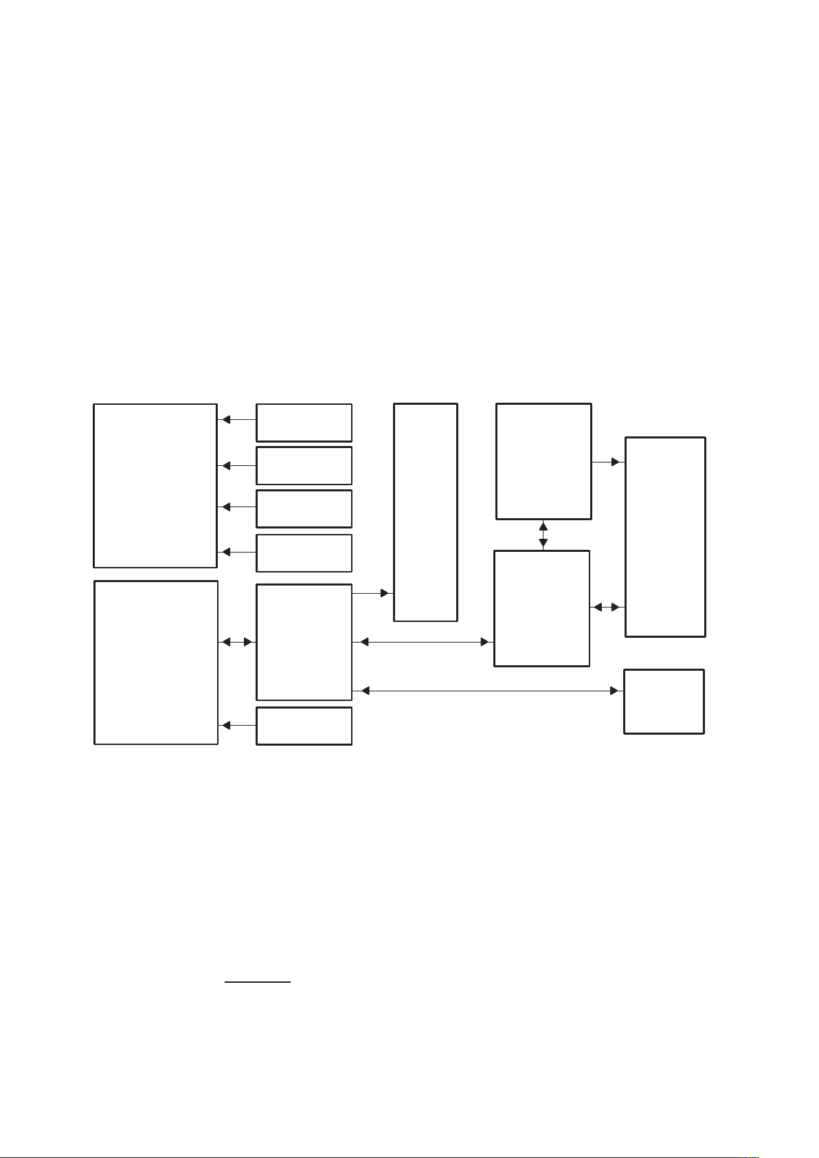
3 PCI2040 Functional Description
This section covers the functional description for PCI2040. The PCI2040 provides a 32-bit PCI host interface and an
interface for 8-bit and 16-bit host port interface (HPI) ports for TI’s C54x and C6x families of DSP processors. The
following conventions are used in this document:
• DSP C54x or C6x
• Word 16 bits for PCI, 16 bits for C54x, 32 bits for C6x
• Half-word 8 bits for C54x, 16 bits for C6x
• Double-word 32 bits for PCI
Figure 3–1 shows a simplified block diagram of the PCI2040.
PCI Host Bus Interface
Miscellaneous
Interface
CPCI Hot-Swap
PCI Power
Management
Serial ROM
GPIO
Interrupt
PCI
Target
SM
HPI
Interface
Registers
&
PCI
Registers
C6x
Host
Port
Extensions
C54x
Host
Port
SM
HPI Interface
GP BUS
Interface
Figure 3–1. PCI2040 System Block Diagram
3.1 PCI Interface
PCI2040 provides an integrated 32-bit PCI bus interface compliant with the
PCI Local Bus Specification
. The PCI2040
incorporates a PCI target interface for configuration cycles, accesses to internal registers, and access to the HPI
interface via memory-mapped space. The PCI2040 does not provide PCI mastering.
As a PCI bus target, PCI2040 incorporates the following features:
• Supports the memory read, memory write, configuration read, and configuration write
• Aliases the memory read multiple, memory read line, and memory write and invalidate to the basic
memory commands (i.e., memory read and memory write)
• Supports PCI_LOCK

3–2
3.2 Accessing Internal PCI2040 Registers
PCI configuration space is accessed via PCI configuration read and PCI configuration write cycles. These registers
may be accessed using byte, word, or double-word transfers.
The PCI2040 provides a set of registers specifically for interfacing with the HPI port. These registers are called the
HPI control and status registers (HPI CSRs) (see Section 5), and they may be memory- and I/O-mapped. The HPI
CSR memory base address register (see Section 4.11) provides the mechanism for mapping the HPI CSRs into
memory space. When mapped into memory space, the HPI CSRs may be accessed using bytes, words, or
double-word transfers. Memory mapping the HPI CSR registers is recommended.
The HPI control and status registers may also be mapped into I/O space via the HPI CSR I/O base address register
(see Section 4.32). When this register is programmed to a nonzero value, PCI2040 maps the HPI CSRs into I/O
space, and the index/data access scheme is used to access the registers using byte transfers.
The HPI CSR I/O base address register identifies the I/O address of the index port. I/O address index + 1 is the data
port. To access a HPI CSR register, software writes the of fset of the HPI CSR register into the index port. I/O reads
from the data port provide the contents of the indexed register and writes to the data port result in PCI2040 updating
the indexed register.
3.3 PCI_LOCK
PCI2040 supports exclusive access via the LOCK protocol defined by PCI and the PCI_LOCK terminal. As a PCI
target, PCI2040 locks all DSP access and internal resources to a particular master when PCI_LOCK
is sampled
deasserted during the address phase of a PCI cycle that it claims. Once LOCK is established, the PCI2040 remains
locked until both FRAME and LOCK are sampled deasserted or bit 30 (HPIError) is set in the interrupt event register
(see Section 5.1).
The master that owns the exclusive access lock on PCI2040 drives PCI_LOCK while the lock is established and
deasserts PCI_LOCK (and asserts FRAME) when addressing the PCI2040. The PCI2040 claims and retries cycles
addressed to it when PCI_LOCK
is asserted. Other masters will not be able to force the PCI_LOCK signal high when
addressing a locked PCI2040 and will be retried.
Note that when the PCI2040 is not locked, it can claim and complete data transfers even if PCI_LOCK is sampled
asserted in the address phase.
3.4 Serial ROM Interface
The PCI2040 provides a two-wire serial ROM interface that may be used to preload PCI2040 registers following a
power-on reset (GRST
). The serial ROM interface includes a serial clock (SCL) output and a serial data (SDA)
input/output. The SCL signal maps to the GPIO0 terminal and the SDA signal maps to the GPIO1 terminal. The
two-wire serial ROM interface is enabled by pulling up both GPIO0 and GPIO1 terminals to VCC with resistors. The
PCI2040 will only sense GPIO0 on GRST to identify the serial ROM; thus, only GPIO0 must be tied low to disable
the serial ROM interface.
The registers that may be preloaded are given in the following list, and only write accessible bits in these registers
may be preloaded. Figure 3–2 illustrates the PCI2040 serial ROM data format.
• Class code register : SubClass – SubClass
• Class code register : BaseClass – BaseClass
• Subsystem vendor ID register – SubSys Byte 0 & SubSys Byte 1
• Subsystem ID register – SubSys Byte 2 & SubSys Byte 3
• GPIO select register – GPIO select register
• Miscellaneous control register – Misc Ctrl Byte 0 & Misc Ctrl Byte 1

3–3
• Diagnostic register – Diagnostic
• HPI DSP implementation register – HPI_Imp Byte 0
• HPI data width register – HPI_DW Byte 0
SubClass
BaseClass
SubSys Byte 0
SubSys Byte 1
SubSys Byte 2
SubSys Byte 3
GPIO Select
RSVD
RSVD
Misc Ctrl Byte 0
Misc Ctrl Byte 1
Diagnostic
HPI_Imp Byte 0
RSVD
HPI_DW Byte 0
RSVD
Word Address 0
Word Address 1
Word Address 2
Word Address 3
Word Address 4
Word Address 5
Word Address 6
Word Address 7
Word Address 8
Word Address 9
Word Address 10
Word Address 11
Word Address 12
Word Address 13
Word Address 14
Word Address 15
RSVD
RSVD
RSVD
RSVD
RSVD
RSVD
RSVD
RSVD
RSVD
RSVD
RSVD
RSVD
RSVD
RSVD
RSVD
RSVD_DIAG
Word Address 16 (10h)
Word Address 17
Word Address 18
Word Address 19
Word Address 20
Word Address 21
Word Address 22
Word Address 23
Word Address 24
Word Address 25
Word Address 26
Word Address 27
Word Address 28
Word Address 29
Word Address 30
Word Address 31
...AVAIL...
Figure 3–2. PCI2040 Serial ROM Data Format
When PCI2040 accesses an implemented serial ROM, it always addresses the serial ROM at slave address
8’b10100000. The serial ROM data format described above utilizes 32 bytes of address space, some of which are
reserved for future generations of the PCI2040. A byte at address 31 is reserved for diagnostic software purposes
and will not be allocated to future generations of the PCI2040. Serial ROM addresses above word address 31 are
available for use by PCI2040 applications. If the data at word address 0 is FFh, then the PCI2040 will stop reading
from the serial ROM. This feature prevents the uninitialized data from being loaded into the PCI2040’s registers.
3.5 PCI2040 Host Port Interface
The PCI2040 HPI interface is used to access TI’s TMS320C54X or TMS320C6X DSP chips. The devices connected
to the HPI interface are memory-mapped in host memory. The host system processor accesses the HPI interface
via slave accesses to PCI2040. The DSP devices can generate interrupts, and the PCI2040 passes these interrupt
requests to the PCI bus via INTA
. See Section 3.7,
Interrupts
, for more information on PCI2040 interrupts.
The HPI port on DSP devices is a parallel port that allows access to the DSP’s memory space and internal registers.
The PCI2040 has to configure the HPI interface on the DSP by accessing the DSP’s HPI control register (HPIC). Other
DSP HPI registers include the HPI data register (HPID) and the HPI address register (HPIA). See Section 6,
DSP
HPI Overview
for more information on DSP registers.
3.5.1 Identifying Implemented Ports and DSP Types
The PCI2040 supports up to four DSPs of both the C54x and C6x types. It may be useful for generic software to
discover what number and type of DSPs are connected to the PCI2040. This is accomplished by using the HPI DSP
implementation register (see Section 5.5) and HPI data width register (see Section 5.6) in the HPI control and status
register space. The HPI DSP implementation register identifies how many DSPs are implemented and what HCSn
outputs are connected, and the HPI data width register identifies whether the HPI port per connected DSP is 8 bits
(C54x) or 16 bits (C6x).

3–4
The HPI DSP implementation register and HPI data width register may be loaded from a serial ROM. Also, these
registers are implemented as read/write so intelligent software can load them with the proper values.
3.5.2 DSP Chip Selects
The PCI2040 provides four chip select outputs (HCS3–HCS0) that uniquely select each HPI port DSP (or other HPI
peripheral) per transaction. This section describes how software encodes the chip select in the PCI address to access
a particular DSP interfacing with PCI2040.
The PCI2040’s control space base address register (see Section 4.12) is a standard PCI base address register
requesting 32K bytes of control space nonprefetchable memory to access up to four DSPs. The PCI2040 claims PCI
memory access transactions that fall within the 32-Kbyte memory window by comparing the upper 17 bits of the PCI
address (PCI_AD31–PCI_AD15) to bits 31–15 (A V AIL_ADD field) in the control space base address register . When
a cycle is claimed, the chip select is determined by decoding bits 14 and 13 of the PCI address. PCI_AD14 and
PCI_AD13 determine the chip select according to Table 3–1.
Only when the PCI cycle is claimed (by decoding PCI_AD31–PCI_AD15) is the chip select asserted.
Table 3–1. PCI2040 Chip Select Decoding
PCI_AD(14–13) CHIP SELECT ASSERTED
2’b00 HCS0
2’b01 HCS1
2’b10 HCS2
2’b11 HCS3
3.5.3 HPI Register Access Control
The HCNTL1 and HCNTL0 terminals are driven by the PCI2040 to select the DSP HPI register and access mode
on a cycle-by-cycle basis. The PCI2040 determines the type of DSP register access from the PCI address, similarly
to the chip select decode as described in Section 3.5.2,
DSP Chip Selects
.
When a cycle is claimed by decoding PCI_AD31–PCI_AD15, the HCNTL1 and HCNTL0 control signals are
determined by decoding bits 12 and 11 of PCI address. PCI_AD12 maps to HCNTL1 and PCI_AD11 maps to
HCNTL0, and the selected HCNTL1 and HCNTL0 are driven to the HPI interface when the cycle is forwarded.
Table 6–1 and Table 6–3 provides more information on the usage of HCNTL1 and HCNTL0 for both C54x and C6x
DSPs.
3.5.4 Mapping HPI DSP Memory to the Host
The PCI address bits PCI_AD10–PCI_AD0 are not forwarded to the HPI interface, and these address bits are not
decoded by PCI2040 for any purpose. This 2-Kbyte of addressable space per DSP (and control) allows the host to
directly map 2K bytes of host memory to the HPI interface for each DSP. This allows for fast memory block copies
rather than an I/O port mechanism.
The PCI2040 does not automatically generate accesses to the HPI address registers based upon
PCI_AD10–PCI_AD0, and it is left to software to synchronize the HPI address register with copies to and from HPI
memory space.
3.5.5 Read/Write Procedure
The following procedure illustrates how to read and write HPI space, and covers some of the initialization that must
be done to successfully transfer data to and from DSP memory via the HPI data register.
After a power-on reset (GRST):
• PCI2040 preloads several registers if a serial ROM is implemented, and this rewrites the HPI
implementation and HPI data width registers (software can also rewrite these registers).

3–5
• HPI CSR memory base address register (see Section 4.1 1) is programmed to provide a pointer to the HPI
control and status registers (see Section 5). HPI CSR I/O base address register (see Section 4.32) can also
be programmed to give I/O access.
• Control space base address register (see Section 4.12) is programmed and 32K bytes of memory are
allocated.
• The PCI command register (see Section 4.3) is programmed to allow PCI2040 to respond to memory and
I/O cycles.
• Software must clear the HPI reset register (see Section 5.4) to remove the reset assertion to the DSPs.
• When PCI2040 decodes a PCI address within the 32-Kbyte memory control space window, it claims the
cycle and decodes the chip select, HCNTL1 and HCNTL0, to pass to the HPI interface.
• The host initializes the BOB or HWOB bit in the HPI control register (see Section 6.2 or Section 6.3.5,
respectively) to choose the correct byte alignment. This results in an HPI cycle to the DSP’s HPI control
register.
• The host then initializes the HPI address register with the correct HPI memory address. By loading the HPI
address register, an internal DSP HPI memory access is initiated and the data is latched in the HPI data
register.
• If this is a read:
– The host performs a read of the HPI data register. During the read, the contents of the first half-word data
latch appear on the HADn pins when the HWIL signal is low and contents of the second data latch when
the HWIL signal is high.
– If auto-increment is selected, then it occurs between the transfer of the first and second bytes. This
allows back-to-back HPI data register accesses without an intervening HPI address register access.
• If this is a write:
– The first data latch of HPI data register is written from the data coming from the host while HWIL is low
and the second data latch when HWIL is high. If communicating with C6x, then the correct combination
of byte enables must also be used.
– If auto-increment is selected, then it occurs between the transfer of the first and second bytes.
3.5.6 HPI Interface Specific Notes
The PCI2040 supports the HPI features from C54x and C6x interfaces given in Table 3–2. See Section 6,
DSP HPI
Overview
, and the
HPI functional specification
and timing requirements for more details.
Table 3–2. HPI Interface Features
C54x C6x
Shared access mode (SAM) and host only mode (HOM) Only one mode of operation: host only mode (HOM)
Auto-increment Auto-increment
Endian byte swap (BOB) Endian byte swap (HWOB)
DSP-to-host interrupt DSP-to-host interrupt
Wait states using HRDY5xn Wait states using HRDY6xn
Two data strobes: HDS, HR/W Two data strobes: HDS, HR/W
HPI memory access during reset Byte enables
No software handshaking using HRDY and FETCH
Valid byte enables All byte enables valid

3–6
3.6 General-Purpose I/O Interface
The PCI2040 has six general-purpose input/output (GPIO) terminals for design flexibility , and these terminals reside
in the V
CCP
signaling environment. GPIO5–GPIO0 default to inputs, but may be programmed to be outputs via the
GPIO direction control register (see Section 4.23). When GPIOx is selected as an input, the logical value of the data
input on GPIOx is reported through the GPIO input data register (see Section 4.22). When GPIOx is selected as an
output, the logical value of the data driven by PCI2040 to the GPIOx terminal is programmed via the GPIO output
data register (see Section 4.24). The GPIO input data register, GPIO output data register , and GPIO direction control
register are only meaningful for GPIOx if GPIOx is selected as a general-purpose input/output through the GPIO
select register (see Section 4.21).
Through the GPIO select register, the GPIO5–GPIO0 terminals may be programmed to other signal functions, such
as test outputs and general-purpose interrupt event inputs. See Section 4.21,
GPIO select register
, for more details
on these options.
If bit 5 in the miscellaneous control register is set to 1 (see Section 4.26), then GPIO5 and GPIO4 provide some
signals from the general-purpose bus interface. Also note that GPIO0 and GPIO1 provide the serial ROM interface
if enabled as described in Section 3.4,
Serial ROM Interface
.
3.7 Interrupts
The PCI2040 reports two classes of interrupts: DSP interrupts and device interrupts. DSP interrupts are generated
when an implemented DSP asserts its HINTn signal, and device interrupts come directly from the remaining PCI2040
logic. For example, one such PCI2040 device interrupt indicates that a serious error has occurred on the HPI
interface.
3.7.1 Interrupt Event and Interrupt Mask Registers
The PCI2040 contains two 32-bit registers to report and control interrupts: interrupt event register (see Section 5.1)
and interrupt mask register (see Section 5.2). These registers exist in the HPI control and status register space. Both
registers have two addresses: a set address and a clear address. For a write to either register, a 1 written to the set
address causes the corresponding bit in the register to be set (excluding bits that are read-only), while a 1 written
to the clear address causes the corresponding bit to be cleared. For both addresses, writing a 0 has no effect on the
corresponding bit in the register.
The interrupt event register contains the actual PCI2040 interrupt request bits, and the response to these sources
can be tested by diagnostic software by setting the corresponding bit in the interrupt event set register. The interrupt
mask register is AND’ed with the interrupt event register to enable selected sources to generate host interrupts
through INT A
. Software writes to the interrupt event clear register to clear interrupt conditions reported in the interrupt
event register.
Reading either the set or the clear address for these registers returns the value of the register with one exception.
Reading the interrupt event clear register returns the value of the interrupt event register AND’ed with the interrupt
mask register to report the unmasked bits that are set in the interrupt event register that caused the interrupt event.
Software can then write this value to the interrupt event clear register, which clears the events causing the interrupt,
and the PCI2040 deasserts INTA if no more unmasked interrupt events are pending.
PCI2040 also implements a global interrupt enable in the interrupt mask register at bit 31 (masterIntEnable). Only
when bit 31 is set will the PCI2040 generate an INTA
.
3.7.2 DSP-to-Host Interrupts
These interrupts are the most common interrupts generated by the PCI2040. The four interrupt events,
IntDSP3–IntDSP0 (bits 3–0 in Section 5.2), occur when the corresponding HINT3–HINT0 is asserted by the DSP.
When enabled via the corresponding bits in the interrupt mask register (see Section 5.1), these DSP interrupts are
passed directly to the PCI host.

3–7
As a side note, HINT is generated when the HINT bit is set in the HPI control register. See Section 6,
DSP HPI
Overview
, for a description of the DSPs HPI control register.
3.7.3 HPI Error Interrupts and HPI Error Reporting
Bit 30 (HPIError) in the interrupt event register (see Section 5.1), set upon serious error conditions on the HPI
interface, allows software to gracefully terminate communication with an HPI device. Bit 30 is set when any of the
bits in the HPI error report register (see Section 5.3) are set (an OR combination).
Bits 3–0 (HPIErr[3:0] field) in the HPI error report register (see Section 5.3) are set for an HPI interface when a cycle
destined for a particular interface experienced as serious error, which may be a result of a DSP losing power. Such
error conditions are as follows:
1. HRDY5xn (or HRDY6xn) driven by DSP is not asserted within 256 PCI clock cycles following assertion
of HCSn. This timer can be disabled by setting bit 1 (ErrorTimer) in the diagnostic register (see
Section 4.27).
2. The discard timeout expires for a read transaction from HPI(x)
3. A PCI byte enable combination other than 4’b1100, 4’b001 1, or 4’b0000 was received for a transaction
destined for a C54x DSP on HPI(x)
T o avoid potential system level catastrophe when the PCI target abort is signaled, PCI2040 implements a feature to
disable target aborts and returns zero data on such error conditions. This mode of operation is enabled via bit 30
(HPIError) in the interrupt mask register (see Section 5.2). When bit 31 is set and bit 30 (HPIError) in the interrupt
event register is also set, on all HPI error conditions, an INTA
interrupt is signaled.
Also when bit 30 (HPIError) in the interrupt mask register is set, error on posted writes will not cause the SERR signal
assertion by bit 8 (SERR_EN) in the PCI command register (see Section 4.3). When bit 30 (HPIError) is 0, target
aborts may occur and SERR may be signaled as a result of a posted write error. This mode of operation is not related
to SERR
signaling on PCI address parity errors per the
PCI Local Bus Specification
.
Future generations of PCI2040 may support connections to different numbers of DSPs (more or less than 4). A
recommended procedure for software to determine the maximum number of DSP HPI connections is to write all 1s
to the HPI error report register and read back the number of set bits. Similarly, software can perform the same
procedure on the lower 16 bits of the interrupt mask or interrupt event register.
3.7.4 General-Purpose Interrupts
The GPIO3 and GPIO2 terminals may be configured via the GPIO select register (see Section 4.21) as general
interrupt event inputs. The general interrupt event type may be either input low signal or input state change, and is
programmable via the GPIO interrupt event type register (see Section 4.25). When these general interrupt events
occur, the corresponding bits 28 (IntGPIO3) and 27 (IntGPIO2) are set in the interrupt event register (see Section 5.1)
and may be enabled to generate an interrupt (INTA
) via interrupt mask register (see Section 5.2).
3.7.5 Interrupts Versus PME
When an unmasked interrupt event occurs and PCI2040 is in the D0 power state, PCI2040 asserts INTA to signal
the interrupt event. When PCI2040 is in D1, D2, or D3, INT A generation is disabled regardless of the value of bit 31
(masterIntEnable) in the interrupt mask register (see Section 5.2).
Whenever an unmasked interrupt event occurs and bit 15 (PME_STS) in the power management control/status
register is set (see Section 4.31), a PME power management event is generated if bit 8 (PME_EN) in the power
management control/status register is set.
3.8 PCI2040 Power Management
This section covers the power management aspects of PCI2040, including descriptions of power savings features.

3–8
3.8.1 PCI Power Management Register Interface
PCI2040 is
PCI Bus Power Interface Management Specification
Revision 1.0 and 1.1 compliant. By default, PCI2040
provides the PCI power management PM 1.0 register set which is documented in Section 4.30. PCI2040 may be
programmed to provide a PCI PM 1.1 register set by setting bit 4 (PM11_EN) of the miscellaneous control register
to 1 (see Section 4.26).
The PCI power management register changes required to provide PCI PM 1.1 compliance to the power management
capabilities register (see Section 4.30) are summarized in Table 3–3.
Table 3–3. PMC Changes for PCI PM 1.1 Register Model
BIT FIELD NAME TYPE DESCRIPTION
15–9 PM 1.0 Compliant Same as PM 1.0 Implementation. No change.
8–6 Aux_Current R
Aux_Current. This field reports the Vaux requirements for PCI2040. If bit 15
(D3cold_PMESupport) in the power management capabilities register is set (see Section 4.30),
then this field returns 3’b001 indicating that PCI2040 draws a maximum of 55 mA while
programmed to D3. If bit 15 (D3cold_PMESupport) is 0, then this field returns 3’b000 since no
wake from D3
cold
is supported.
Bit 6 is aliased to bit 15 and is read-only.
5 PM 1.0 Compliant R Same as PM 1.0 Implementation. No change.
4 RSVD R
This reserved field returns 0 when read in the PCI PM 1.1 register model and returns 1 when
read in the PCI PM 1.0 model.
3 PM 1.0 Compliant R Same as PM 1.0 Implementation. No change.
2–0 Version R
These three bits return 010b when read, indicating that there are 4 bytes of general-purpose
power management (PM) registers as described in the draft revision 1.1
PCI Bus Power
Management Interface Specification
.
3.8.2 PCI Power Management Device States and Transitions
PCI2040 supports all D0–D3 device power states, and can assert PME from any power state including D3
cold
when
V aux is supplied. The PCI2040’s power state implementation is simply disabling the HPI state machine when in the
D1, D2, or D3 power states. D0 is the fully operational power state.
If an HPI cycle initiated by PCI2040 is in progress when bits 1 and 0 (PWRST ATE field) in the power management
control/status register are programmed to D1, D2, or D3 (see Section 4.31), then the PCI2040 will complete the cycle
in progress before transitioning to the lower power state.
On a transition to the D0 power state from the D3 power state, PCI2040 asserts an internal signal equivalent to a
PCI_RST
which does not reset all internal states. There are several register bits that are reset by GRST versus the
PCI_RST, and these are referred to as the PME context (or sometimes sticky) bits.
The PME context bits for PCI2040 are listed below and Figure 3–3 illustrates the relationship between the PME
context bits: GRST, and PCI_RST. The addition of GRST allows for retaining device state from a D3 to D0 transition
when the PCI interface may transition from B3 to B0 and issue a PCI reset.
PCI2040 PME
context bits for PCI space:
• 0x0A – SubClass Code register (all implemented bits)
• 0x0B – BaseClass Code register (all implemented bits)
• 0x2C – Subsystem vendor ID register (all implemented bits)
• 0x2E – Subsystem ID register (all implemented bits)
• 0x44 – GPIO select register (all implemented bits)
• 0x46 – GPIO direction control register (all implemented bits)
• 0x47 – GPIO output data register (all implemented bits)

3–9
• 0x48 – GPIO interrupt type register (all implemented bits)
• 0x4C – Miscellaneous control register (all implemented bits)
• 0x4C – Diagnostic register (all implemented bits)
• 0x52 – Power management capabilities register (D3cold_PMESupport)
• 0x54 – Power management control/status register (PMCSR.PME_STS, PMCSR.PME_ENB)
PCI2040 PME context bits for HPI CSR space:
• 0x00 / 0x04 – Interrupt event register (all implemented bits)
• 0x08 / 0x0C – Interrupt mask register (all implemented bits)
• 0x10 – HPI error report register (all implemented bits)
• 0x14 – HPI reset register (all implemented bits)
• 0x16 – HPI implementation register (all implemented bits)
• 0x18 – HPI data width register (all implemented bits)
RESET
PCI_RST
Non-PME Context
PME
Context
GRST
RESET
Figure 3–3. PCI2040 Reset Illustration
3.9 Compact PCI Hot-Swap
PCI2040 is hot-swap friendly silicon that will support all the hot-swap capable features, contain support for software
control, and integrate circuitry required by the
Compact PCI Hot Swap Specification PICMG 2.1
. To be hot-swap
capable, PCI2040 supports the following:
•
PCI Local Bus Specification, Revision 2.1
compliance
• VCC from early power tolerant
• Asynchronous reset
• Precharge voltage tolerant
• I/O buffers must meet modified V/I requirements
• Limited I/O pin voltage at precharge voltage
• Hot swap control and status programming via extended PCI capabilities linked list
• Hot swap terminals: HSENUM, HSSWITCH, and HSLED
CPCI hot-swap defines a process for installing and removing PCI boards without adversely affecting a running
system. The PCI2040 provides this functionality such that it can be implemented on a board that can be removed
and inserted in a hot-swap system.
The PCI2040 provides three terminals to support hot-swap: HSENUM
(output), HSSWITCH (input), and HSLED
(output). The HSENUM output indicates to the system that an insertion event occurred or that a removal event is about
to occur. The HSSWITCH input indicates that state of a board ejector handle, and the HSLED output lights a blue
LED to signal insertion and removal ready status.
The PCI2040 hot-swap functionality is controlled via the CPCI hot swap control and status register (see Section 4.35)
in extended PCI configuration space. This register provides four bits for control: bit 7 (INS), bit 6 (EXT), bit 3 (LOO),

3–10
and bit 1 (EIM). Since no HSSWITCH status is provided in the CPCI hot swap control and status register, PCI2040
provides bit 8 (HSSWITCH_STS) in the miscellaneous control register (see Section 4.26).
HSENUM
is an active low open drain output that is asserted when either bit 7 (INS) or bit 6 (EXT) are set and bit 1
(EIM, the HSENUM
mask bit) is cleared. For the insertion event, PCI2040 will drive HSLED after PCI_RST until the
serial ROM preload is complete and the ejector handle is closed (HSSWITCH_STS is 0). When these conditions are
met, the HSLED is under software control via bit 3 (LOO). Bit 7 (INS) is set when the conditions described above are
met and bit 6 (EXT) is 0. Thus, bit 7 (INS) is set following an insertion when the board implementing PCI2040 is ready
for configuration and cannot be set by software.
For the removal event, bit 6 (EXT) is set when the ejector handle is opened (HSSWITCH_STS is 1) and bit 7 (INS)
is 0. This will cause HSENUM to be asserted if bit 1 (EIM) is 0, and software will halt connection with PCI2040 and
light the LED via bit 3 (LOO). The board may then be safely removed.
See the
Compact PCI Hot Swap Specification PICMG 2.1
for more details.
3.10 General-Purpose Bus
This section discusses the general-purpose interface of PCI2040. This is a 16-bit data and a 6-bit address bus. The
6-bit address bus is mapped directly to PCI address bits 7–2. This means that each address on the GP bus
corresponds to a 32-bit (1 DW) address on the PCI bus for a total of 256 bytes of addressable space. Because the
GP bus is only a 16-bit data bus, only the lower 16 bits (15–0) of the PCI data bus is used. In other words, the only
valid byte enable combination is 1100b.
The general-purpose bus read/write strobes must default to the JTAG TBC (8990) timing requirements. However,
GP_RDY
signal can be used to extend the use of the bus for slower devices.
Most of the GP bus signals are multiplexed onto the HPI bus as described in the table below. In addition to the
multiplexed signals, there are three dedicated GP bus signals which are GPINT, GPRDY, and GPRST.
T able 3–4. General-Purpose Bus Signals
HPI SIGNALS GP BUS SIGNALS TYPE NOTES
HAD15–HAD0 GP_DATA15–GP_DATA0 I/O GP data bus. A 16-bit data bus
HBE0 GPA0 O One of the six address lines
HBE1 GPA1 O One of the six address lines
HWIL GPA2 O One of the six address lines
HCNTL0 GPA3 O One of the six address lines
HCNTL1 GPA4 O One of the six address lines
HR/W GPA5 One of the six address lines
HDS GP_CS O GP chip select. This signal is asserted during an access on the GP bus.
GPIO5 GP_RD O
GP read strobe. This active low signal indicates a read from a device on the bus. The
data on the bus is valid on the rising edge of GP_RD
.
GPIO4 GP_WR O
GP write strobe. This active low signal indicates a write to a device on the bus. The
data on the bus is valid on the rising edge of GP_WR
.
Terminal 74 GP_INT I GP interrupt. Interrupt from a device on the GP bus.
Terminal 75 GP_RDY I
GP ready. Whenever the device on the GP bus is ready to accept a read or write from
PCI2040, GP_RDY
is asserted. RDY is deasserted when the device is in recovery
from a read or write operation.
Terminal 70 GP_RST O GP reset. An active low output that follows the state of GRST.

3–11
3.11 Example Transactions on the General-Purpose Bus
This section describes some example transactions on the GP bus.
3.11.1 General-Purpose Bus Word Write
The first diagram, Figure 3–4, depicts a word (16–bits) write to a device residing on the GP bus. The event flow is
as follows:
1. All signals are in a deasserted state except for GP_RDY . The PCI2040 is driving the address and data bus
to a stable but unknown value.
2. The GP_CS
is driven low. The data bus (GPD15–GPD0) is driven with the data the PCI2040 obtained from
the PCI bus. In this case, the data is BBAAh. The address bus (GPA5–GPA0) is driven with the address
the PCI2040 obtained from the PCI bus. For example, if the address on the PCI bus is FF0B0h, then this
address would translate to a GP bus address of 2Ch.
3. The GP_WR strobe is driven low indicating a write to the device on the GP bus.
4. The GP_WR strobe is driven high. Typically, a device on the GP bus latches the data on the rising edge
of the GP_WR strobe. But as the figure shows, the data is valid on both the falling edge and the rising edge
of the write strobe. The PCI2040 samples the GP_RDY signal before it deasserts the GP_WR strobe. In
this case, the GP_RDY
signal is low indicating to the PCI2040 that the device is ready for data.
5. The transaction completes by deasserting the GP_CS.
PCI_CLK
GP_RST
GP_CS
GPD[15:0]
GPA[5:0]
GP_WR
GP_RD
GP_RDY
BBAA
2C
1 2345
Figure 3–4. General-Purpose Bus Word Write
3.11.2 General-Purpose Bus Word Read
The second diagram, Figure 3–5, shows a word read from a device on the GP bus. The event flow is as follows:
1. All signals are in a deasserted state except for GP_RDY
. The PCI2040 is driving the address and data bus
to a stable but unknown value.
2. The GP_CS is driven low. The data bus (GPD15–GPD0) is placed in a high impedance state. The address
bus is driven with the address the PCI2040 obtained from the PCI bus.
3. The GP_RD strobe is driven low indicating a read to the device on the GP bus. Sometime later during
clock 3, the device on the GP bus drives valid data on the data bus.
4. The GP_RD strobe is driven high. The PCI2040 samples the GP_RDY before it deasserts GP_RD. If
GP_RDY is sampled asserted, then the PCI2040 deasserts GP_RD strobe and latches the data on the GP
bus. If GP_RDY is sampled deasserted, then the PCI2040 keeps GP_RD asserted and waits for the
GP_RDY
strobe to be asserted before it deasserts the GP_RD strobe.

3–12
5. The transaction completes by deasserting the GP_CS. The PCI2040 starts driving the GP address and data
bus with stable values.
PCI_CLK
GP_RST
GP_CS
GPD[15:0]
GPA[5:0]
GP_WR
GP_RD
GP_RDY
ZZZZ BBAA ZZZZ
2C
12345
Figure 3–5. General-Purpose Bus Word Read

4–1
4 PCI2040 Programming Model
This section describes the PCI2040 PCI configuration registers that make up the 256-byte PCI configuration header.
A brief description is provided for each register, followed by the register of fset and a default state for each register.
The bit table also has reserved fields that contain read-only reserved bits. These bits return 0s when read.
4.1 PCI Configuration Registers
The PCI2040 is a device that interfaces the PCI bus to the 8-bit or 16-bit HPI port of T exas Instruments C54x or C6x
family of DSP processors. The configuration header is compliant with the
PCI Local Bus Specification
.
The configuration header is compliant with the
PCI Local Bus Specification
as a type 0 bridge header, and is PC98/99
compliant as well. Table 4–1 shows the PCI configuration header, which includes both the predefined portion of the
configuration space and the user-definable registers.
Table 4–1. PCI Configuration Registers
REGISTER NAME OFFSET
Device ID Vendor ID 00h
Status Command 04h
Class code Revision ID 08h
BIST Header type Latency timer Cache line size 0Ch
HPI CSR memory base address 10h
Control space base address 14h
GPBus base address 18h
Reserved 1Ch
Reserved 20h
Reserved 24h
Reserved 28h
Subsystem ID Subsystem vendor ID 2Ch
Reserved 30h
Reserved Reserved Reserved Capability pointer 34h
Reserved 38h
Max_Lat Min_GNT Interrupt pin Interrupt line 3Ch
Reserved Reserved 40h
GPIO output data GPIO direction control GPIO input data GPIO select 44h
Reserved Reserved Reserved GPIO interrupt type 48h
Diagnostic Reserved Miscellaneous control 4Ch
Power management capabilities PM next-item pointer PM capability ID 50h
Reserved PM control/status 54h
HPI CSR I/O base address 58h
Reserved HS_CSR HS next-item pointer HS capability ID 5Ch
Reserved Reserved Reserved Reserved 60h
Reserved 64h–FFh
NOTE: Optional registers not implemented for PCI2040 return 0s when read.

4–2
A bit description table is typically included that indicates bit field names, a detailed field description, and field access
tags. Table 4–2 describes the field access tags.
Table 4–2. Bit Field Access Tag Descriptions
ACCESS
TAG
NAME MEANING
R Read Field may be read by software.
W Write Field may be written by software to any value.
S Set Field may be set by a write of 1. Writes of 0 have no effect.
C Clear Field may be cleared by a write of one. Writes of 0 have no effect.
U Update Field may be autonomously updated by PCI2040.
4.2 Vendor and Device ID Register
The vendor and device ID register returns AC60104Ch when read which consists of a unique device ID assigned by
TI (AC60h) and a value assigned by the PCI SIG to Texas Instruments (104Ch).
Bit 31 30 29 28 27 26 25 24 23 22 21 20 19 18 17 16
Name Device ID
Type R R R R R R R R R R R R R R R R
Default 1 0 1 0 1 1 0 0 0 1 1 0 0 0 0 0
Bit 15 14 13 12 11 10 9 8 7 6 5 4 3 2 1 0
Name Vendor ID
Type R R R R R R R R R R R R R R R R
Default 0 0 0 1 0 0 0 0 0 1 0 0 1 1 0 0
Register: Vendor and device ID
Type: Read-only
Offset: 00h
Default: AC60104Ch

4–3
4.3 PCI Command Register
The system software accesses the status and command registers for error recovery, diagnostic, and control. This
register is provided to enable coarse control over a device’s ability to generate and respond to PCI cycles.
Bit 15 14 13 12 11 10 9 8 7 6 5 4 3 2 1 0
Name PCI command
Type R R R R R R R RW R RW R R R R RW RW
Default 0 0 0 0 0 0 0 0 0 0 0 0 0 0 0 0
Register: PCI command
Type: Read-only, Read/Write
Offset: 04h
Default: 0000h
T able 4–3. PCI Command Register
BIT FIELD NAME TYPE DESCRIPTION
15–10 RSVD R Reserved. Bits 15–10 return 0s when read.
9 FBB–EN R
Fast back-to-back (FBB) enable. This bit controls whether or not the device is allowed to perform
back-to-back capability for bus master transaction. This bit is hardwired to 0 and indicates that FBB
transfers are not supported by PCI2040.
8 SERR_EN RW
System error (SERR) enable. This bit is an enable for the output driver on the SERR pin. If this bit is
cleared and a system error condition is set inside PCI2040, then the error signal will not appear on the
external SERR
pin.
7 STEP_EN R
Address/data stepping control. This bit indicates whether or not the device performs address stepping.
Since the PCI2040 does not require address stepping, this bit is hardwired to 0.
6 PERR_EN RW
Parity error response enable. This bit controls whether or not the device responds to detected parity
errors. If this bit is set, then the PCI2040 responds normally to parity errors. If this bit is cleared, then
the PCI2040 ignores detected parity errors.
5 VGA_EN R VGA palette snoop. This bit is not applicable for PCI2040 and is hardwired to a 0.
4 MWI_EN R
Memory write and invalidate enable. This bit enables the device to use the memory write and invalidate
command. Since the PCI2040 does not support MWI but uses MW instead, this bit is hardwired to 0.
3 Special R
Special cycle. This bit controls the device’s response to special cycle commands. Since PCI2040 does
not monitor any special commands, this bit is set to 0.
2 MAST_EN R
Bus master control. This bit allows a PCI device to function as a bus master. This bit is always 0 indicating
PCI2040 does not support PCI mastering.
1 MEM_EN RW
Memory space enable. This bit enables the device to respond to memory accesses to any of the defined
base address memory regions. If this bit is cleared, then the PCI2040 will not respond to
memory-mapped accesses.
0 IO_EN RW
I/O space control. This bit enables the device to respond to I/O accesses within its defined base address
register I/O regions.

4–4
4.4 PCI Status Register
The PCI status register provides the host information to the host system. A bit in this register is reset when 1 is written
to it. A 0 written to a bit has no effect.
Bit 15 14 13 12 11 10 9 8 7 6 5 4 3 2 1 0
Name PCI status
Type RC RC R R RC R R R R R R R R R R R
Default 0 0 0 0 0 0 1 0 0 0 0 1 0 0 0 0
Register: PCI status
Type: Read-only, Read/Write to Clear
Offset: 06h
Default: 0210h
Table 4–4. PCI Status Register
BIT FIELD NAME TYPE DESCRIPTION
15 PAR_ERR RC Detected parity error. This bit is set by the PCI2040 to indicate that it detected a parity error.
14 SYS_ERR RC
Signaled system error. This bit is set by the PCI2040 to indicate that it signaled a system error on the
SERR
pin. This bit can be reset by writing a 1.
13 MABORT R Receive master abort. This bit is set to indicate a transaction has been terminated due to a master abort.
12 TABT_REC R Receive target abort. This bit is set when a transaction is terminated by a target abort.
11 TABT_SIG RC
Signaled target abort. This bit is set by the PCI slave unit in the PCI2040 to indicate that it has initiated
a target abort.
10–9 PCI_SPEED R
DEVSEL timing. Bits 10 and 9 encode the timing of DEVSEL and are hardwired to 01b indicating that
the PCI2040 asserts PCI_SPEED at a medium speed on nonconfiguration cycle accesses.
8 DATAPAR R
Data parity error detected. This bit is implemented by the bus mastering devices to indicate that a parity
error has been detected.
7 FBB_CAP R
Fast back-to-back capable. This bit indicates that the device is capable of performing fast back-to-back
transactions. Since the PCI2040 does not support fast back-to-back transactions, this bit is hardwired
to 0.
6 UDF R User definable feature support. Bit 6 is hardwired to 0 indicating that the PCI2040 does not support UDF.
5 66MHZ R 66-MHz capable. Bit 5 is hardwired to 0 indicating that the PCI2040 does not support 66 MHz operations.
4 CAPLIST R
Capabilities list. Bit 4 returns 1 when read indicating that capabilities in addition to standard capabilities
are implemented.
3–0 RSVD R Reserved. Bits 3–0 return 0s when read.
4.5 Revision ID
This register indicates the silicon revision of the PCI2040.
Bit 7 6 5 4 3 2 1 0
Name Revision ID
Type R R R R R R R R
Default 0 0 0 0 0 0 0 0
Register: Revision ID
Type: Read-only
Offset: 08h
Default: 00h

4–5
4.6 Class Code
The class code register categorizes the function as a bridge device (06h), and another bridge device (80h) with a
standard programming interface (00h). Subclass and base class are loaded via serial ROM.
Bit 23 22 21 20 19 18 17 16 15 14 13 12 11 10 9 8 7 6 5 4 3 2 1 0
Name Class code
Base class Subclass Programming interface
Type R R R R R R R R R R R R R R R R R R R R R R R R
Default 0 0 0 0 0 1 1 0 1 0 0 0 0 0 0 0 0 0 0 0 0 0 0 0
Register: Class code
Type: Read-only
Offset: 09h
Default: 068000h
4.7 Cache Line Size Register
The cache line size register is programmed by the host software to indicate the cache line size.
Bit 7 6 5 4 3 2 1 0
Name Cache line size
Type RW RW RW RW RW RW RW RW
Default 0 0 0 0 0 0 0 0
Register: Cache line size
Type: Read/Write
Offset: 0Ch
Default: 00h
4.8 Latency Timer Register
The latency timer register returns 0s when read since the PCI2040 is a target-only device.
Bit 7 6 5 4 3 2 1 0
Name Latency timer
Type R R R R R R R R
Default 0 0 0 0 0 0 0 0
Register: Latency timer
Type: Read-only
Offset: 0Dh
Default: 00h

4–6
4.9 Header Type Register
The header type register returns 00h when read, indicating that the PCI2040 configuration space adheres to the
standard PCI header and it is a single function device.
Bit 7 6 5 4 3 2 1 0
Name Header type
Type R R R R R R R R
Default 0 0 0 0 0 0 0 0
Register: Header type
Type: Read-only
Offset: 0Eh
Default: 00h
4.10 BIST Register
The PCI2040 does not support built-in-self-test (BIST); therefore, this register returns 00h when read.
Bit 7 6 5 4 3 2 1 0
Name BIST
Type R R R R R R R R
Default 0 0 0 0 0 0 0 0
Register: BIST
Type: Read-only
Offset: 0Fh
Default: 00h

4–7
4.11 HPI CSR Memory Base Address Register
The HPI CSR memory base address register provides a method of allowing the host to map the PCI2040’s HPI CSR
registers into host memory space.
Bit 31 30 29 28 27 26 25 24 23 22 21 20 19 18 17 16
Name HPI CSR memory base address
Type RW RW RW RW RW RW RW RW RW RW RW RW RW RW RW RW
Default 0 0 0 0 0 0 0 0 0 0 0 0 0 0 0 0
Bit 15 14 13 12 11 10 9 8 7 6 5 4 3 2 1 0
Name HPI CSR memory base address
Type RW RW RW RW R R R R R R R R R R R R
Default 0 0 0 0 0 0 0 0 0 0 0 0 0 0 0 0
Register: HPI CSR memory base address
Type: Read-only, Read/Write
Offset: 10h
Default: 0000 0000h
T able 4–5. HPI CSR Memory Base Address Register
BIT FIELD NAME TYPE DESCRIPTION
31–12 AVAIL_ADD RW
Available address bits. These bits can be written by the host in order to allow initialization of the base
address at startup. The PCI memory address space is on the 4-Kbyte boundary.
11–4 UNAVAIL_ADD R Unavailable address bit. Bits 11–4 return 00h when read.
3 PREFETCHABLE R Prefetchable. This bit is hardwired to 0 in the PCI2040.
2–1 TYPE R
Type. Bits 2 and 1 indicate the size of the base address and how it can be mapped into the host memory .
These bits are hardwired to 00 in the PCI2040 to indicate that a 32-bit base address register is used
which can be located anywhere in memory.
0 MEM_IND R
Memory space indicator. This bit indicates whether the base address maps into the host’ s memory or
I/O space. This bit is hardwired to 0 in the PCI2040 to indicate that this base address is valid only for
memory accesses.

4–8
4.12 Control Space Base Address Register
The control space base address register allows the host to map the PCI2040’s 32K bytes of control space into host
memory .
Bit 31 30 29 28 27 26 25 24 23 22 21 20 19 18 17 16
Name Control space base address
Type RW RW RW RW RW RW RW RW RW RW RW RW RW RW RW RW
Default 0 0 0 0 0 0 0 0 0 0 0 0 0 0 0 0
Bit 15 14 13 12 11 10 9 8 7 6 5 4 3 2 1 0
Name Control space base address
Type RW R R R R R R R R R R R R R R R
Default 0 0 0 0 0 0 0 0 0 0 0 0 0 0 0 0
Register: Control space base address
Type: Read-only, Read/Write
Offset: 14h
Default: 0000 0000h
Table 4–6. Control Space Base Address Register
BIT FIELD NAME TYPE DESCRIPTION
31–15 AVAIL_ADD RW
Available address bits. Bits 31–15 allow the host to map the PCI2040’s 32K bytes of control space into
memory. See Sections 3.5.2,
DSP Chip Selects
, and 3.5.3,
HPI Register Access Control
, for details
on addressing the control space.
14–4 RSVD R Reserved. Bits 14–4 return 0s when read.
3 PREFETCHABLE R Prefetchable. This bit is hardwired to 0 in the PCI2040. The control space is not prefetchable.
2–1 TYPE R
Type. Bits 2 and 1 indicate the size of the base address and how it can be mapped into the host memory .
These bits are hardwired to 00 in the PCI2040 to indicate that a 32-bit base address register is used
which can be located anywhere in memory.
0 MEM_IND R
Memory space indicator. This bit indicates whether the base address maps into the host’ s memory or
I/O space. This bit is hardwired to 0 in the PCI2040 to indicate that the control space is
memory-mapped.

4–9
4.13 GP Bus Base Address Register
The GP bus base address register is used by the PCI2040 to communicate with a device on the GP bus. This 32–bit
register allows software to assign a memory window for the GP bus anywhere in the 4-Gbyte address space. This
window has a 256-byte granularity which means the lower 8 bits of this register default to 0 and are read-only . This
register is controlled via bit 5 (GP_EN) in the miscellaneous control register (see Section 4.26) and if it is set to 0,
then this register will be read-only and always return 0000 0000h when read.
Bit 31 30 29 28 27 26 25 24 23 22 21 20 19 18 17 16
Name GP bus base address
Type RW RW RW RW RW RW RW RW RW RW RW RW RW RW RW RW
Default 0 0 0 0 0 0 0 0 0 0 0 0 0 0 0 0
Bit 15 14 13 12 11 10 9 8 7 6 5 4 3 2 1 0
Name GP bus base address
Type RW RW RW RW RW RW RW RW R R R R R R R R
Default 0 0 0 0 0 0 0 0 0 0 0 0 0 0 0 0
Register: GP bus base address
Type: Read-only, Read/Write
Offset: 18h
Default: 0000 0000h
T able 4–7. General-Purpose Bus Base Address Register
BIT FIELD NAME TYPE DESCRIPTION
31–8 AVAIL_ADD RW
Available address bits. Bits 31–8 allow the host to map the PCI2040’s 128 bytes of control space into
memory.
7–4 RSVD R Reserved. Bits 7–4 return 0s when read.
3 PREFETCHABLE R Prefetchable. This bit is hardwired to 0 in the PCI2040. The control space is not prefetchable.
2–1 TYPE R
Type. Bits 2–1 indicate the size of the base address and how it can be mapped into the host memory .
These bits are hardwired to 00 in the PCI2040 to indicate that a 32-bit base address register is used
which can be located anywhere in memory.
0 MEM_IND R
Memory space indicator. This bit indicates whether the base address maps into the host’ s memory or
I/O space. This bit is hardwired to 0 in the PCI2040 to indicate that this register is memory-mapped.
4.14 Subsystem Vendor ID Register
The subsystem vendor ID register is used for system identification purposes and may be required for certain operating
systems. This register is read-only or read/write depending on the value of bit 0 (SUBSYSRW) in the miscellaneous
control register (see Section 4.26). When bit 0 (SUBSYSRW) is 0, this register is read/write and when bit 0 is 1, this
register is read-only. This register may be loaded from the serial ROM.
Bit 15 14 13 12 11 10 9 8 7 6 5 4 3 2 1 0
Name Subsystem vendor ID
Type R R R R R R R R R R R R R R R R
Default 0 0 0 0 0 0 0 0 0 0 0 0 0 0 0 0
Register: Subsystem vendor ID
Type: Read-only
Offset: 2Ch
Default: 0000h

4–10
4.15 Subsystem ID Register
The subsystem ID register is used for system identification purposes and may be required for certain operating
systems. This register is read-only or read/write depending on the value of bit 0 (SUBSYSRW) in the miscellaneous
control register (see Section 4.26). When bit 0 (SUBSYSRW) is 0, this register is read/write and when bit 0 is 1, this
register is read-only. This register may be loaded from the serial ROM.
Bit 15 14 13 12 11 10 9 8 7 6 5 4 3 2 1 0
Name Subsystem ID
Type R R R R R R R R R R R R R R R R
Default 0 0 0 0 0 0 0 0 0 0 0 0 0 0 0 0
Register: Subsystem ID
Type: Read-only
Offset: 2Eh
Default: 0000h
4.16 Capability Pointer Register
The capability pointer register provides a pointer into the PCI configuration header where the PCI power management
block resides.
Bit 7 6 5 4 3 2 1 0
Name Capability pointer
Type R R R R R R R R
Default 0 1 0 1 0 0 0 0
Register: Capability pointer
Type: Read-only
Offset: 34h
Default: 50h
4.17 Interrupt Line Register
The interrupt line register is written by the host and indicates to which input of the system interrupt controller the
PCI2040’s interrupt pin is connected.
Bit 7 6 5 4 3 2 1 0
Name Interrupt line
Type RW RW RW RW RW RW RW RW
Default 1 1 1 1 1 1 1 1
Register: Interrupt line
Type: Read/Write
Offset: 3Ch
Default: FFh

4–11
4.18 Interrupt Pin Register
The interrupt pin register tells which interrupt the device uses. This register is hardwired to 01h in the PCI2040 to
indicate that INTA will be used.
Bit 7 6 5 4 3 2 1 0
Name Interrupt pin
Type R R R R R R R R
Default 0 0 0 0 0 0 0 1
Register: Interrupt pin
Type: Read-only
Offset: 3Dh
Default: 01h
4.19 MIN_GNT Register
This register specifies the length of the burst period for the device needs in 0.25 µsec units. The default value for this
register is 00h as the PCI2040 is a target-only device.
Bit 7 6 5 4 3 2 1 0
Name MIN_GNT
Type R R R R R R R R
Default 0 0 0 0 0 0 0 0
Register: MIN_GNT
Type: Read-only
Offset: 3Eh
Default: 00h
4.20 MAX_LAT Register
This register specifies how often the device needs to gain access to the PCI bus in 0.25 µsec units. The default value
for this register is 00h as the PCI2040 is a target-only device.
Bit 7 6 5 4 3 2 1 0
Name MAX_LAT
Type R R R R R R R R
Default 0 0 0 0 0 0 0 0
Register: MAX_LAT
Type: Read-only
Offset: 3Fh
Default: 00h

4–12
4.21 GPIO Select Register
The GPIO select register is used to program the GPIOx terminal functions.
Bit 7 6 5 4 3 2 1 0
Name GPIO select
Type R R RU RU RW RW RW RW
Default 0 0 0 0 0 0 0 0
Register: GPIO select
Type: Read/Update/Write
Offset: 44h
Default: 00h
T able 4–8. GPIO Select Register
BIT FIELD NAME TYPE DESCRIPTION
7–6 RSVD R Reserved. Bits 7 and 6 return 0s when read.
5 GPIO5Pin RU
GPIO5 pin. The value of this pin determines the function of GPIO5.
0 = Normal GPIO data (default)
1 = GP_RD
. Read strobe (RD) for the GP bus. The PCI2040 will set this bit when bit 5 (GP_EN) in the
miscellaneous control register is set (see Section 4.26). Clearing bit 5 (GP_EN) will automatically
clear this bit.
4 GPIO4Pin RU
GPIO4 pin. The value of this pin determines the function of GPIO4.
0 = Normal GPIO data (default)
1 = GPWR
. Write strobe (WR) for the GP bus. The PCI2040 will set this bit when bit 5 (GP_EN) in the
miscellaneous control register is set (see Section 4.26). Clearing bit 5 (GP_EN) will automatically
clear this bit.
3 GPIO3Pin RW
GPIO3 pin. The value of this pin determines the function of GPIO3. When programmed as an interrupt
event input, the event is selected in the GPIO interrupt event type register (see Section 4.25). When
programmed as a normal GPIO, the IntGPIO3 interrupt event will never occur.
0 = Normal GPIO data (default)
1 = GPIO3 is an interrupt event input
2 GPIO2Pin RW
GPIO2 pin. The value of this pin determines the function of GPIO2. When programmed as an interrupt
event input, the event is selected in the GPIO interrupt event type register (see Section 4.25). When
programmed as a normal GPIO, the IntGPIO2 interrupt event will never occur.
0 = Normal GPIO data (default)
1 = GPIO2 is an interrupt event input
1 GPIO1Pin R
GPIO1 pin. The value of this pin determines the function of GPIO1.
0 = Normal GPIO data (default)
1 = Reserved.
0 GPIO0Pin R
GPIO0 pin. The value of this pin determines the function of GPIO0.
0 = Normal GPIO data (default)
1 = Reserved.

4–13
4.22 GPIO Input Data Register
The GPIO input data register reflects the state of the GPIO pins, and defaults to an unknown value.
Bit 7 6 5 4 3 2 1 0
Name GPIO input data
Type R R R R R R R R
Default 0 0 X X X X X X
Register: GPIO input data
Type: Read-only
Offset: 45h
Default: XXh
Table 4–9. GPIO Input Data Register
BIT FIELD NAME TYPE DESCRIPTION
7–6 RSVD R Reserved. Bits 7 and 6 return 0s when read.
5–0 GPIO[5:0] Pin State R GPIO5–GPIO0 pin state. Returns the logical value of the data input to the GPIO5–GPIO0 terminals.
4.23 GPIO Direction Control Register
The GPIO direction control register controls the direction of GPIO pins.
Bit 7 6 5 4 3 2 1 0
Name GPIO direction control
Type R R RW RW RW RW RW RW
Default 0 0 0 0 0 0 0 0
Register: GPIO direction control
Type: Read-only, Read/Write
Offset: 46h
Default: 00h
Table 4–10. GPIO Direction Control Register
BIT FIELD NAME TYPE DESCRIPTION
7–6 RSVD R Reserved. Bits 7 and 6 return 0s when read.
5–0
GPIO[5:0] Direction
Control
RW
GPIO5–GPIO0 direction control. When the GPIOn direction control bit is set, then the GPIOn signal
is an output. When the GPIOn direction control bit is 0, the GPIOn signal is an input.

4–14
4.24 GPIO Output Data Register
The GPIO output data register contains the output data for any selected output pin.
Bit 7 6 5 4 3 2 1 0
Name GPIO output data
Type R R RW RW RW RW RW RW
Default 0 0 0 0 0 0 0 0
Register: GPIO output data
Type: Read-only, Read/Write
Offset: 47h
Default: 00h
Table 4–11. GPIO Output Data Register
BIT FIELD NAME TYPE DESCRIPTION
7–6 RSVD R Reserved. Bits 7 and 6 return 0s when read.
5–0
GPIO[5:0] Output
data
RW
GPIO5–GPIO0 output data.
0 = Data out value, if selected, is 0 (default)
1 = Data out value, if selected, is 1.
4.25 GPIO Interrupt Event Type Register
The GPIO interrupt event type register gives the status of GPIO routed through INTA.
Bit 7 6 5 4 3 2 1 0
Name GPIO interrupt event type
Type R R R R RW RW R R
Default 0 0 0 0 0 0 0 0
Register: GPIO interrupt event type
Type: Read-only, Read/Write
Offset: 48h
Default: 00h
Table 4–12. GPIO Interrupt Event Type Register
BIT FIELD NAME TYPE DESCRIPTION
7–4 RSVD R Reserved. Bits 7–4 return 0s when read.
3 GPIO3INTYPE RW
GPIO3 interrupt type.
0 = Bit 28 (IntGPIO3) in the interrupt event register (see Section 5.1) is set when GPIO3 input is
low (default)
1 = Bit 28 (IntGPIO3) in the interrupt event register (see Section 5.1) is set when GPIO3 input
changes state
2 GPIO2INTYPE RW
GPIO2 interrupt type.
0 = Bit 27 (IntGPIO2) in the interrupt event register (see Section 5.1) is set when GPIO2 input is
low (default)
1 = Bit 27 (IntGPIO2) in the interrupt event register (see Section 5.1) is set when GPIO2 input
changes state
1–0 RSVD R Reserved. Bits 1–0 return 0s when read.

4–15
4.26 Miscellaneous Control Register
The miscellaneous control register controls various miscellaneous functions.
Bit 15 14 13 12 11 10 9 8 7 6 5 4 3 2 1 0
Name Miscellaneous control
Type RU RCU R R R R R R R R RW RW RW RW RW RW
Default 0 0 0 0 0 0 0 0 0 0 0 0 1 1 1 1
Register: Miscellaneous control
Type: Read/Clear/Update/Write
Offset: 4Ch
Default: 000Fh
Table 4–13. Miscellaneous Control Register
BIT FIELD NAME TYPE DESCRIPTION
15 SEEDS RU
Serial EEPROM detect status. When this bit is set, it indicates that serial EEPROM block has detected
an EEPROM.
14 SEEBES RCU
Serial EEPROM error status. When set, an error has occurred on the serial ROM interface. Writing a
1 to this bit clears the error status.
13 SEEBS R Serial EEPROM busy status. When set, the serial ROM interface is busy.
12–9 RSVD R Reserved. Bits 12–9 return 0s when read.
8 HSSWITCH_STS R
Hot swap switch status. Returns logical value of HSSWITCH input.
0 = Handle closed
1 = Handle open
7–6 RSVD R Reserved. Bits 7–6 return 0s when read.
5 GP_EN R
GP bus enable.
0 = GP bus disabled. (default)
1 = GP bus enabled.
4 PM11_EN R
PCI PM Specification 1.1 enable.
0 = Use PCI PM 1.0 register implementation (Default)
1 = Use PCI PM 1.1 register implementation
3 HSEN R
Hot swap enable.
0 = Hot swap disabled
1 = Hot swap enabled (default)
2 D3COLD_LOCK R
Lock bit for PME support from D3
cold
.
0 = Bit 15 (D3cold_PMESupport) in the power management capabilities register is read/write
(see Section 4.30)
1 = Bit 15 (D3cold_PMESupport) in the power management capabilities register is read-only
(default) (see Section 4.30)
1 PWDIS R
Posted write disable bit.
0 = Posted writes are disabled
1 = Posted writes are enabled (default)
0 SUBSYSRW R
Subsystem read write enable.
0 = Subsystem ID and subsystem vendor ID registers are read/write
1 = Subsystem ID and subsystem vendor ID registers are read-only (default)

4–16
4.27 Diagnostic Register
The diagnostic register is provided for test purposes and should not be accessed during normal operation.
Bit 7 6 5 4 3 2 1 0
Name Diagnostic
Type RW R R RW RW R RW RW
Default 0 0 0 0 0 0 0 0
Register: Diagnostic
Type: Read/Write
Offset: 4Fh
Default: 00h
Table 4–14. Diagnostic Register
BIT FIELD NAME TYPE DESCRIPTION
7 TRUE_VAL RW True value. When set, all 1s are returned in the PCI vendor and device ID registers.
6–5 RSVD R Reserved. Bits 6–5 return 0s when read.
4 DIAG4 RW
Diagnostic RETRY_DIS. Delayed transaction disable. When bit 4 is set, delayed transactions are
disabled. When bit 4 is 0 (default), they are enabled.
3 DIAG3 RW
Diagnostic RETRY_EXT . When set, the PCI2040 extends the target latency from 16 to 64 PCI clocks and
is not
PCI Local Bus Specification, Revision 2.2
compliant.
2 RSVD R Reserved. Bit 2 returns 0 when read.
1 ErrorTimer RW
Error timer. Bit 1 is used to enable/disable the error timer. By default, the timer is enabled but can be
disabled by writing a 1 to this bit.
0 TI_TEST RW
TI_TEST_BIT. This is internal TI test bit used by the design.
0 = Disable state vectors to GPIOs (default)
1 = Enable state vectors to GPIOs
4.28 PM Capability ID Register
The PM capability ID register identifies the linked list item as the register for PCI power management. This register
returns 01h when read, which is the unique ID located by the PCI SIG for the PCI location of the capabilities pointer
and the value.
Bit 7 6 5 4 3 2 1 0
Name PM capability ID
Type R R R R R R R R
Default 0 0 0 0 0 0 0 1
Register: PM capability ID
Type: Read-only
Offset: 50h
Default: 01h

4–17
4.29 PM Next-Item Pointer Register
The PM next-item pointer register provides a pointer into the PCI configuration header where the CPCI hot swap
control and status register (HS_CSR) resides. The PCI header at 5Ch provides the hot swap register. If bit 3 (HSEN)
in the miscellaneous control register (see Section 4.26) is 0, then the PM next-item pointer register returns 00h when
read indicating the end of the extended capability list.
Bit 7 6 5 4 3 2 1 0
Name PM next-item pointer
Type R R R R R R R R
Default 0 1 0 1 1 1 0 0
Register: PM next-item pointer
Type: Read-only
Offset: 51h
Default: 5Ch
4.30 Power Management Capabilities Register
The power management capabilities (PMC) register contains information on the capabilities of the PCI2040 related
to power management. The PCI2040 supports all D0–D3 power states.
Bit 15 14 13 12 11 10 9 8 7 6 5 4 3 2 1 0
Name Power management capabilities
Type R R R R R R R R R R R R R R R R
Default 1 1 1 1 1 1 1 0 0 0 0 1 0 0 0 1
Register: Power management capabilities
Type: Read-only
Offset: 52h
Default: FE11h
Table 4–15. Power Management Capabilities Register
BIT FIELD NAME TYPE DESCRIPTION
15 D3cold_PMESupport R(W)
D3
cold
PME support. This bit defaults to read-only and becomes read/write when bit 2
(D3COLD_LOCK) in the miscellaneous control register is set (see Section 4.26). This bit defaults
to 1 indicating the PME
signal can be asserted from the D3
cold
state. This bit is read/write
because wake-up support from D3
cold
is contingent on the system providing an auxiliary power
source to the Vcc terminals. If auxiliary power is not provided to Vcc terminals for D3
cold
wake-up,
then this bit should be cleared. This bit is not reset by the assertion of PCI_RST
, but is reset by
GRST
.
14–11 PME Support R
This field has a value of 4’b111 1 indicating that the PCI2040 can signal PME from the D3
hot
, D2,
D1 and D0 states.
10 D2_Support R This bit returns a 1 when read indicating that the PCI2040 supports D2.
9 D1_Support R This bit returns a 1 when read indicating that the PCI2040 supports D1.
8–6 RSVD R Reserved. Bits 8–6 return 0s when read.
5 DSI R
Device specific initialization. This bit returns 0 when read indicating no special initialization is
required before a standard driver can use the PCI2040.
4 AUX_PWR R
Auxiliary power source. Bit 4 returns 1 when read indicating PME support in D3
cold
requires an
auxiliary power source.
3 PMECLK R
This bit returns 0 when read indicating that no PCI clock is required for the function to generate
PME
.
2–0 Version R
These three bits return 001b when read indicating compliance to
PCI Bus Power Management
Interface Specification
.

4–18
4.31 Power Management Control/Status Register
The power management control/status register determines and changes the current power state of the PCI2040. The
contents of this register are not affected by the internally generated reset caused by the transition from the D3
hot
to
D0 state. All PCI registers will be reset as a result of a D3
hot
-to-D0 state transition. TI specific registers, PCI power
management registers, and the legacy base address register are not reset.
Bit 15 14 13 12 11 10 9 8 7 6 5 4 3 2 1 0
Name Power management control/status
Type RCU R R R R R R RW R R R R R R RW RW
Default 0 0 0 0 0 0 0 0 0 0 0 0 0 0 0 0
Register: Power management control/status
Type: Read/Clear/Update/Write
Offset: 54h
Default: 0000h
Table 4–16. Power Management Control/Status Register
BIT FIELD NAME TYPE DESCRIPTION
15 PME_STS RCU
PME status. This bit is set when the PME signal is asserted, independent of the state of bit 8 (PME_EN).
This bit is cleared by a write back of 1, and this also clears the PME
signal if PME was asserted. Writing
a 0 to this bit has no effect. This bit will NOT be cleared by the assertion of PCI_RST
. It will only be cleared
by the assertion of GRST
.
14–13 DATASCALE R Data scale. This two-bit field returns 0s when read.
12–9 DATASEL R Data select. This four-bit field returns 0s when read.
8 PME_EN RW
PME enable. This bit enables the function to assert PME. If bit 8 is cleared, then assertion of PME is
disabled. Bit 8 is NOT cleared by the assertion of PCI_RST
. It is only cleared by the assertion of GRST.
7–2 RSVD R Reserved. Bits 7–2 return 0s when read.
1–0 PWRSTATE RW
Power state. This two-bit field is used both to determine the current power state of a function, and to set
the function into a new power state. This field is encoded as:
00 = D0
01 = D1
10 = D2
11 = D3
hot

4–19
4.32 HPI CSR I/O Base Address Register
The PCI2040 supports the index/data scheme of accessing the HPI CSR registers. An address written to this register
is the address for the index register and the address + 1 is the data address. The base address can be mapped
anywhere in 32-bit I/O space on a word boundary except at address 0x0000; hence, bit 0 is read-only, returning 0
when read.
The HPI CSR I/O base address is only meaningful when a nonzero value is written into this register.
Bit 31 30 29 28 27 26 25 24 23 22 21 20 19 18 17 16
Name HPI CSR I/O base address
Type RW RW RW RW RW RW RW RW RW RW RW RW RW RW RW RW
Default 0 0 0 0 0 0 0 0 0 0 0 0 0 0 0 0
Bit 15 14 13 12 11 10 9 8 7 6 5 4 3 2 1 0
Name HPI CSR I/O base address
Type RW RW RW RW RW RW RW RW RW RW RW RW RW RW RW R
Default 0 0 0 0 0 0 0 0 0 0 0 0 0 0 0 0
Register: HPI CSR I/O base address
Type: Read-only, Read/Write
Offset: 58h
Default: 0000 0000h
T able 4–17. HPI CSR I/O Base Address Register
BIT FIELD NAME TYPE DESCRIPTION
31–1 HPICSR_IO_BAR RW
Available address bits. These bits can be written by the host in order to allow initialization of the base
address at startup.
0 RSVD R Reserved. Bit 0 returns 0 when read for word alignment.
4.33 HS Capability ID Register
The HS capability ID register identifies the linked list item as the register for CompactPCI hot swap. This register
returns 06h when read which is the unique ID assigned by the PCI SIG for the PCI location of the capabilities pointer
and the value.
Bit 7 6 5 4 3 2 1 0
Name HS capability ID
Type R R R R R R R R
Default 0 0 0 0 0 1 1 0
Register: HS capability ID
Type: Read-only
Offset: 5Ch
Default: 06h

4–20
4.34 HS Next-Item Pointer Register
The HS next-item pointer register is used to indicate the next item in the linked list of the PCI extended capabilities.
This register returns 00h indicating no additional capabilities are supported.
Bit 7 6 5 4 3 2 1 0
Name HS next-item pointer
Type R R R R R R R R
Default 0 0 0 0 0 0 0 0
Register: HS next-item pointer
Type: Read-only
Offset: 5Dh
Default: 00h
4.35 CPCI Hot Swap Control and Status Register
The CPCI hot swap control and status register (HS_CSR) provides the control and status information about the
compact PCI hot swap resources.
Bit 7 6 5 4 3 2 1 0
Name CPCI hot swap control and status
Type RCU RCU R R RW R RW R
Default 0 0 0 0 0 0 0 0
Register: CPCI hot swap control and status
Type: Read/Clear/Update/Write
Offset: 5Eh
Default: 00h
Table 4–18. CPCI Hot Swap Control and Status Register
BIT FIELD NAME TYPE DESCRIPTION
7 INS RCU
ENUM insertion status. When set, the HSENUM output is driven by the PCI2040. This bit defaults to 0, and
will be set after a PCI_RST
occurs, the preload of serial ROM is complete (miscellaneous control register,
bit 13 [SEEBS] is 0), the ejector handle is closed (miscellaneous control register, bit 8 [HSSWITCH_STS] is
0), and bit 6 (EXT) is 0. Thus, this bit is set following an insertion when the board implementing the PCI2040
is ready for configuration. This bit cannot be set under software control.
6 EXT RCU
ENUM extraction status. When set, the HSENUM output is driven by the PCI2040. This bit defaults to 0, and
is set when the ejector handle is opened (miscellaneous control register, bit 8 [HSSWITCH_STS] is 1) and bit 7
(INS) is 0. Thus, this bit is set when the board implementing the PCI2040 is about to be removed. This bit cannot
be set under software control.
5–4 RSVD R Reserved. Bits 5 and 4 return 0s when read.
3 LOO RW
LED on/off. This bit defaults to 0, and controls the external LED indicator (HSLED) under normal conditions.
However, for a duration following a PCI_RST
, the HSLED output is driven high by the PCI2040 control and this
bit will be ignored. When this bit is interpreted, a 1 will cause HSLED high and a 0 will cause HSLED low.
Following PCI_RST
, the HSLED output is driven high by the PCI2040 until both the pre-load of serial ROM
(miscellaneous control register, bit 13 [SEEBS] is 0), and the ejector handle is closed (miscellaneous control
register, bit 8 [HSSWITCH_STS] is 0). When these conditions are met, the HSLED is under software control
via bit 3 (LOO).
2 RSVD R Reserved. Bit 2 returns 0 when read.
1 EIM RW
ENUM interrupt mask. This bit allows the HSENUM output to be masked by software. Bits 7 (INS) and 6 (EXT)
are set independently from bit 1.
0 = Enable HSENUM
output
1 = Mask HSENUM
output
0 RSVD R Reserved. Bit 0 returns 0 when read.

5–1
5 HPI Control and Status Registers
This section covers the PCI2040 HPI control and status register (HPI CSR) space. The PCI2040 allows software to
access the HPI configuration through either memory or I/O address space. The memory base address is
programmable via the HPI CSR base address register (PCI offset 10h). The I/O base address is programmable via
the HPI CSR I/O base address register (PCI offset 58h).
Table 5–1. HPI Configuration Register Map
REGISTER NAME OFFSET
Interrupt event set 00h
Interrupt event clear 04h
Interrupt mask set 08h
Interrupt mask clear 0Ch
Reserved HPI error report 10h
HPI DSP implementation HPI reset 14h
Reserved HPI data width 18h

5–2
5.1 Interrupt Event Register
The interrupt event register reflects the state of the various PCI2040 interrupt sources. The interrupt bits are set by
an asserting edge of the corresponding interrupt signal or by writing a 1 in the corresponding bit in the set register.
The only mechanism to clear the bits in this register is to write a 1 to the corresponding bit in the clear register. Note
that the interrupt event register itself is returned on reads from the interrupt event set register (offset 00h), but the
bit-wise AND of the interrupt event and interrupt mask registers is returned on reads from the interrupt event clear
register (offset 04h).
Bit 31 30 29 28 27 26 25 24 23 22 21 20 19 18 17 16
Name Interrupt event
Type R RU RSCU RSCU RSCU RSCU R R R R R R R R R R
Default 0 0 0 0 0 0 0 0 0 0 0 0 0 0 0 0
Bit 15 14 13 12 11 10 9 8 7 6 5 4 3 2 1 0
Name Interrupt event
Type R R R R R R R R R R R R RSCU RSCU RSCU RSCU
Default 0 0 0 0 0 0 0 0 0 0 0 0 0 0 0 0
Register: Interrupt event
Type: Read/Set/Clear/Update
Offset: 00h Set Register
04h Clear Register [Returns IntEvent & IntMask when read]
Default: 0000 0000h
Table 5–2. Interrupt Event Register
BIT FIELD NAME TYPE DESCRIPTION
31 RSVD R Reserved. Bit 31 returns 0 when read.
30 HPIError RU
Bit 30 is set upon serious error conditions on the HPI interface, and allows software to gracefully terminate
communication with an HPI device. This bit is the OR combination of the HPI errors in the HPI error report
register (see Section 5.3).
29 GPError RSCU
Bit 29 is set upon serious error conditions on the GP interface, and allows software to gracefully terminate
communication with a GP device.
28 IntGPIO3 RSCU
Set when GPIO3Pin (see Section 4.21, bit 3) selects GPIO3 as an interrupt event input, and the event type
selected by the GPIO interrupt event type register occurs (see Section 4.25).
27 IntGPIO2 RSCU
Set when GPIO2Pin (see Section 4.21, bit 2) selects GPIO2 as an interrupt event input, and the event type
selected by the GPIO interrupt event type register occurs (see Section 4.25).
26 GPINT RSCU
The PCI2040 sets this bit if an interrupt has been generated by a device connected to the GPINT interface.
Software can set this bit for diagnostics.
25–4 RSVD R Reserved. Bits 25–4 return 0s when read.
3 IntDSP3 RSCU
The PCI2040 sets this bit if an interrupt has been generated by a device connected to the HPI[3] interface.
Software can set this bit for diagnostics.
2 IntDSP2 RSCU
The PCI2040 sets this bit if an interrupt has been generated by a device connected to the HPI[2] interface.
Software can set this bit for diagnostics.
1 IntDSP1 RSCU
The PCI2040 sets this bit if an interrupt has been generated by a device connected to the HPI[1] interface.
Software can set this bit for diagnostics.
0 IntDSP0 RSCU
The PCI2040 sets this bit if an interrupt has been generated by a device connected to the HPI[0] interface.
Software can set this bit for diagnostics.

5–3
5.2 Interrupt Mask Register
The interrupt mask register is used to enable the various PCI2040 interrupt sources. Reads from either the set register
or the clear register always return interrupt mask. In all cases, except masterIntEnable (bit 31), the enables for each
interrupt event align with the event register bits detailed in Table 5–2.
Bit 31 30 29 28 27 26 25 24 23 22 21 20 19 18 17 16
Name Interrupt mask
Type RSC RSC RSC RSC RSC RSC R R R R R R R R R R
Default 0 0 0 0 0 0 0 0 0 0 0 0 0 0 0 0
Bit 15 14 13 12 11 10 9 8 7 6 5 4 3 2 1 0
Name Interrupt mask
Type R R R R R R R R R R R R RSC RSC RSC RSC
Default 0 0 0 0 0 0 0 0 0 0 0 0 0 0 0 0
Register: Interrupt mask
Type: Read/Set/Clear
Offset: 08h Set Register
0Ch Clear Register
Default: 0000 0000h
Table 5–3. Interrupt Mask Register
BIT FIELD NAME TYPE DESCRIPTION
31 masterIntEnable RSC
When bit 31 is set, external interrupts are generated in accordance with this register . If bit 31 is 0, then
no external interrupts are generated.
30 HPIError RSC
When bit 30 is set and the interrupt event register, HPIError bit (see Table 5–2, bit 30) is also set, an
interrupt is generated. When set, the HPI state machine will never cause target aborts on PCI and will
return the PCI slave 0s on such errors.
When set, errors on posted writes will not cause SERR
signal assertions enabled by bit 8 (SERR_EN)
in the PCI command register (see Section 4.3). When bit 30 is 0, target aborts may occur and SERR
may be signaled as a result of a posted write error.
29 GPError RSC
When bit 29 is set and the interrupt event register, GPError bit (see Table 5–2, bit 29) is also set, an
interrupt is generated. When set, the GP state machine will never cause target aborts on PCI and will
return the PCI slave 0s on such errors. When bits 29 and 30 are set, errors on posted writes will not cause
SERR
signal assertions enabled by bit 8 (SERR_EN) in the PCI command register (see Section 4.3).
Both bits 29 and 30 need to be set to prevent target aborts.
28 IntGPIO3 RSC
When bit 28 is set and the corresponding interrupt event register bit (see Table 5–2, bit 28) is also set,
an interrupt is generated. When bit 28 is 0, the interrupt is masked.
27 IntGPIO2 RSC
When bit 27 is set and the corresponding interrupt event register bit (see Table 5–2, bit 27) is also set,
an interrupt is generated. When bit 27 is 0, the interrupt is masked.
26 GPINT RSC
When bit 26 is set and the corresponding interrupt event register bit (see Table 5–2, bit 26) is also set,
an interrupt is generated. When bit 26 is 0, the interrupt is masked.
25–4 RSVD R Reserved. Bits 25–4 return 0s when read.
3 IntDSP3 RSC
When bit 3 is set and the corresponding interrupt event register bit (see T able 5–2, bit 3) is also set, an
interrupt is generated. When bit 3 is 0, the interrupt is masked.
2 IntDSP2 RSC
When bit 2 is set and the corresponding interrupt event register bit (see T able 5–2, bit 2) is also set, an
interrupt is generated. When bit 2 is 0, the interrupt is masked.
1 IntDSP1 RSC
When bit 1 is set and the corresponding interrupt event register bit (see T able 5–2, bit 1) is also set, an
interrupt is generated. When bit 1 is 0, the interrupt is masked.
0 IntDSP0 RSC
When bit 0 is set and the corresponding interrupt event register bit (see T able 5–2, bit 0) is also set, an
interrupt is generated. When bit 0 is 0, the interrupt is masked.

5–4
5.3 HPI Error Report Register
The HPI error report register reflects the state of errors on the HPI interfaces. If any bits in this register are set, then
the PCI2040 sets bit 30 (HPIError) in the interrupt event register (see Section 5.1). Software can set the bits in this
register for diagnostics.
Bit 15 14 13 12 11 10 9 8 7 6 5 4 3 2 1 0
Name HPI error report
Type R R R R R R R R R R R R RWU RWU RWU RWU
Default 0 0 0 0 0 0 0 0 0 0 0 0 0 0 0 0
Register: HPI error report
Type: Read/Write/Update
Offset: 10h
Default: 0000h
T able 5–4. HPI Error Report Register
BIT FIELD NAME TYPE DESCRIPTION
15–4 RSVD R Reserved. Bits 15–4 return 0s when read.
3–0 HPIErr[3:0] RWU
PCI2040 sets this bit if a serious error occurs on the HPI[x] interface. The error conditions that cause this
bit to be set are as follows:
1. HRDY5xn (or HRDY6xn
) driven by DSPn not sampled asserted within 16 PCI clocks following the
assertion of HCSn
by PCI2040
2. When the discard timeout expires for a read transaction from HPI[x]
3. A PCI byte enable combination other than 4’b1100, 4’b0011, or 4’b0000 was received for a
transaction destined for a C54x DSP on HPI[x]
5.4 HPI Reset Register
The HPI reset register is used to cause resets to the DSP interfaces. The implemented bits in this register are in the
PME context for PCI2040 and default to set. Thus, a GRST causes all DSP interfaces to be reset, and software is
responsible for removing the HRSTn to the DSP interfaces.
Bit 15 14 13 12 11 10 9 8 7 6 5 4 3 2 1 0
Name HPI reset
Type R R R R R R R R R R R R RW RW RW RW
Default 0 0 0 0 0 0 0 0 0 0 0 0 1 1 1 1
Register: HPI reset
Type: Read-only, Read/Write
Offset: 14h
Default: 000Fh
T able 5–5. HPI Reset Register
BIT FIELD NAME TYPE DESCRIPTION
15–4 RSVD R Reserved. Bits 15–4 return 0s when read.
3 HPI3_RST RW HPI reset 3. When bit 3 is set, HRST3 is asserted.
2 HPI2_RST RW HPI reset 2. When bit 2 is set, HRST2 is asserted.
1 HPI1_RST RW HPI reset 1. When bit 1 is set, HRST1 is asserted.
0 HPI0_RST RW HPI reset 0. When bit 0 is set, HRST0 is asserted.

5–5
5.5 HPI DSP Implementation Register
The HPI DSP implementation register is used to indicate the presence of implemented DSPs on the HPI interface
and is loaded from the serial ROM.
Bit 15 14 13 12 11 10 9 8 7 6 5 4 3 2 1 0
Name HPI DSP implementation
Type R R R R R R R R R R R R RWU RWU RWU RWU
Default 0 0 0 0 0 0 0 0 0 0 0 0 0 0 0 0
Register: HPI DSP implementation
Type: Read/Write/Update
Offset: 16h
Default: 0000h
T able 5–6. HPI DSP Implementation Register
BIT FIELD NAME TYPE DESCRIPTION
15–4 RSVD R Reserved. Bits 15–4 return 0s when read.
3 DSP_PRSNT3 RWU DSP3 present. Bit 3 indicates if the DSP3 is present on the HPI interface.
2 DSP_PRSNT2 RWU DSP2 present. Bit 2 indicates if the DSP2 is present on the HPI interface.
1 DSP_PRSNT1 RWU DSP1 present. Bit 1 indicates if the DSP1 is present on the HPI interface.
0 DSP_PRSNT0 RWU DSP0 present. Bit 0 indicates if the DSP0 is present on the HPI interface.
5.6 HPI Data Width Register
The HPI data width register is used to determine if the implemented DSPs are C54x or C6x, and is loaded from the
serial ROM. Each bit in this register is meaningful only if the corresponding bit in the HPI DSP implementation register
is set (see Section 5.5).
Bit 15 14 13 12 11 10 9 8 7 6 5 4 3 2 1 0
Name HPI data width
Type R R R R R R R R R R R R RWU RWU RWU RWU
Default 0 0 0 0 0 0 0 0 0 0 0 0 0 0 0 0
Register: HPI data width
Type: Read/Write/Update
Offset: 18h
Default: 0000h
Table 5–7. HPI Data Width Register
BIT FIELD NAME TYPE DESCRIPTION
15–4 RSVD R Reserved. Bits 15–4 return 0s when read.
3 DWIDTH3 RWU When bit 3 is set, the HPI[3] data bus is 16 bits (C6x). When bit 3 is 0, it is 8 bits (C54x).
2 DWIDTH2 RWU When bit 2 is set, the HPI[2] data bus is 16 bits (C6x). When bit 2 is 0, it is 8 bits (C54x).
1 DWIDTH1 RWU When bit 1 is set, the HPI[1] data bus is 16 bits (C6x). When bit 1 is 0, it is 8 bits (C54x).
0 DWIDTH0 RWU When bit 0 is set, the HPI[0] data bus is 16 bits (C6x). When bit 0 is 0, it is 8 bits (C54x).

5–6

6–1
6 DSP HPI Overview
This section gives an overview of the DSP host port interface (HPI). Refer to the C54x/C6x data sheets for complete
HPI details.
6.1 C54X Host Port Interface
The HPI is an 8-bit parallel port used to interface a host device or host processor to a C54x DSP. Information is
exchanged between the DSP and the host device through on-chip C54x memory that is accessible by both the host
and the DSP.
The HPI is designed to interface to the host device as a peripheral, with the host device as the master of the interface,
and so facilitating the ease of access by the host. The host device communicates with the HPI through dedicated
address and data registers, to which the DSP does not have direct access, and the HPI control register using the
external data and interface control signals. Both host devices and the HPI have access to the HPI control register.
In C54x, the HPI provides 16-bit data to the DSP while maintaining an external interface of 8-bit by automatically
combining the successive bytes into 16-bit words. When the host performs a data transfer with the HPI registers, the
HPI control logic automatically performs an access to DSP’s memory to complete the transaction. The DSP can then
access the data within its memory space.
6.1.1 Modes of Operation
In C54x, the HPI has two modes of operation as follows:
• Shared access mode (SAM): This is the normal mode of operation and in this mode both the DSP and
host can access the HPI memory. In this case, the asynchronous host accesses are resynchronized
internally . In the case of a conflict between the DSP and host, host has access priority and DSP waits
1 cycle. In SAM, the HPI can transfer 1 byte every 5 CLKOUT1 (40 MHz), i.e., 64 Mbps. The HPI is
designed such that the host can take advantage of its high bandwidth and can run up to 32 MHz without
requiring wait states.
• Host only mode (HOM): In this mode, only the host can access the HPI memory while the DSP is in reset
state or IDLE2 with all internal or external clocks stopped. This mode allows host to access the HPI
memory while the DSP is in minimum power consumption configuration. In HOM, the HPI supports
higher speed back-to-back accesses on the order of 1 byte/50 ns (160 Mbps) independent of the DSP’s
clock rate.
6.1.2 HPI Functional Description
In C54x, information is exchanged between the host and the DSP via 8-bit external data bus but, because of the 16-bit
word structure of the C54, all transfers consist of two consecutive bytes. The dedicated HWIL pin indicates whether
the first or second byte is being transferred. Bits 0 and 8 (BOB) in the HPI control register determines whether the
first byte is MSB or LSB. The host must not break the first/second byte sequence, otherwise the data may be lost or
some unpredictable results may happen.
6.1.3 HPI Registers
The HPI utilizes three registers for communication between the host device and the CPU. These registers are:
• HPI address register (HPIA). It is directly accessible only by the host and contains the address in HPI
memory at which the current address access occurs.
• HPI control register (HPIC). It is directly accessed by the host or by C54x and contains the control and
status bits for HPI operation.

6–2
• HPI data register (HPID). This register is directly accessible by the host and contains the data that was
read from the HPI memory if the current access is a read, or the data that will be written to the HPI
memory if the current access is a write.
The two control inputs, HCNTL1 and HCNTL0, indicate which internal register is being accessed as shown below.
T able 6–1. C54X HPI Registers Access Control
HCNTL1 HCNTL0 DESCRIPTION
0 0 PCI2040 read/write to HPI control register.
0 1
PCI2040 read/write to HPI data register. Address auto-increment is
selected.
1 0 PCI2040 read/write to HPI address register.
1 1
PCI2040 read/write to HPI data register. Address auto-increment is
not selected.
HPI control register is a 16-bit register but only 4 bits control the HPI operation. Because the transfer consists of two
consecutive half-words, the HPI control register is organized such that it has the same high and low half-word
contents. The control and status bits are located on the least significant 4 bits. When the host writes to the HPI control
register, both bytes must be the same.

6–3
6.2 C54X HPI Control Register
Bit 15 14 13 12 11 10 9 8 7 6 5 4 3 2 1 0
Name C54X HPI control
Host Type R R R R R/W W R R/W R R R R R/W W R R/W
DSP Type R R R R R/W – R/W – R R R R R/W – R/W –
Default 0 0 0 0 0 0 0 0 0 0 0 0 0 0 0 0
Table 6–2. C54X HPI Control Register Description
BIT FIELD NAME HOST TYPE DSP TYPE FUNCTION
15–12
RSVD
R
R
Reserved. These bits return 0s when read.
11 HINT R/W R/W
This bit determines the state of the DSP HINT output which is used to generate an interrupt
to the host. HINT= 0 after reset. The HINT can be set only by the DSP by writing a 1 to
this bit and can be cleared only by the host writing a 1 to this bit.
10 DSPINT W –
Host to DSP interrupt. This bit can only be written by the host and is not readable by the
host or the DSP . When the host writes a 1 to this bit, an interrupt is generated to the DSP.
Writing a 0 has no effect.
9 SMOD R R/W
This bit determines the mode of operation.
0 = HOM is selected (Always during reset)
1 = SAM is selected
8 BOB R/W –
BOB affects both data and address transfers. Only the host can modify this bit and it is
not visible to the DSP. BOB must be initialized before the first data or address register
access.
0 = First byte is the MS
1 = First byte is the LS
7–4 RSVD R R Reserved. These bits return 0s when read.
3 HINT R/W R/W
This bit determines the state of the DSP HINT output which is used to generate an interrupt
to the host. HINT= 0 after reset. The HINT can be set only by the DSP by writing a 1 to
this bit and can be cleared only by the host writing a 1 to this bit.
2 DSPINT W –
Host to DSP interrupt. This bit can only be written by the host and is not readable by the
host or the DSP . When the host writes a 1 to this bit, an interrupt is generated to the DSP.
Writing a 0 has no effect.
1 SMOD R R/W
This bit determines the mode of operation.
0 = HOM is selected (always during reset)
1 = SAM is selected
0 BOB R/W –
BOB affects both data and address transfers. Only the host can modify this bit and it is
not visible to the DSP. BOB must be initialized before the first data or address register
access.
0 = First byte is MS
1 = First byte is the LS
6.2.1 Auto Increment Feature
The HPI data register can be accessed with optional auto-address increment. It provides a convenient way of reading
or writing to subsequent word locations. In the auto-increment mode, the data read causes a postincrement of the
HPI address register and a data write causes a preincrement of the HPI address register. Because the HPI has
2Kx16-bit memory , it uses only the 1 1 LSBs of the HPI address register but, during the auto-increment operation, all
16 bits will be incremented or decremented.
6.2.2 Interrupts
DSP can interrupt the host by writing to bit 3 (HINT) of the HPI control register. By writing a 1 by the DSP to the HINT
bit of the HPI control register, the HPI can assert its HINT pin that is connected to the HINT pin of PCI2040. The host
can acknowledge and clear this bit by writing a 1 to this bit. Writing a 0 to the HINT bit has no effect.

6–4
A C54x interrupt is generated when the host writes a 1 to the DSPINT bit (bit 2) of the HPI control register. This
interrupt can be used to wake up DSP from IDLE. The host and C54x always read this bit as 0. Once a 1 is written
to DSPINT by the host, a 0 need not be written before generating another interrupt. A DSP write or writing a 0 to this
bit has no effect.
The host should not write a 1 to the DSPINT bit while writing to BOB or HINT and the DSP should not write a 1 to the
HINT bit while writing to SMOD bit or an unwanted interrupt will be generated.
6.2.3 Four Strobes (HDS1, HDS2, HR/W, HAS)
HPI has four strobes and they are:
• Two data strobes (HDS1 and HDS2)
• Read/write strobe (HR/W
)
• Address strobe (HAS)
The HCS input serves primarily as the enable input for the HPI and HDS1 and HDS2 control the HPI data transfer.
The equivalent circuit of these three inputs is shown in the figure below. This figure shows that the internal strobe
signal that samples the HCNTL1, HCNTL0, HWIL, and HR/W (when HAS is not used) is derived from all three input
signals. So the latest of the HCS
, HDS1, and HDS2 control the sampling of these inputs.
HCS
HDS2
HDS1
Internal Strobe
Figure 6–1. C54X Select Input Logic
6.2.4 Wait States
The HPI ready pin (HRDY) allows insertion of wait states to allow deferred completion of access cycles for hosts that
have faster cycle times that the HPI can accept due to C54x operating clock rates. The PCI2040 has four HRDY
signals, one for each DSP. The HRDY signal will automatically adjust the host access rate to a faster DSP clock rate
or switch the HPI mode (to HOM) for faster access.
6.2.5 Host Read/Write Access to HPI
The host begins accessing the HPI interface first by initializing the HPI control register, then by initializing the HPI
address register, and then by reading data from or writing data to the HPI data register. Writing to the HPI address
or HPI data register initiates an internal cycle that transfers the desired data between the HPI data register and the
internal HPI memory . This process may take several cycles. Each time an access is made, data written to HPI data
register is not written to HPI memory until after the host access cycle and the data read from HPI data register is the
data from the previous cycle. Therefore, when reading, the data is obtained from the location specified in the previous
access and the current access serves as an initiation of the next cycle. A similar operation occurs for the write
operation. The data written to the HPI data register is not written to HPI memory until after the external cycle is
completed. If the HPI data register read operation immediately follows an HPI data register write operation, then the
same data (the data written) is read.
During random transfers or sequential transfers selected with auto-increment with a significant amount of time
between them, the HPI address register must be either rewritten, or two reads from the same location must be done,
or an address write prior to read must be made to ensure that the most recent data is read because the DSP may
have changed the contents of the location being accessed.
In SAM, the HRDY signal is used to insert wait states if necessary . However, this signal is inactive in HOM. Unless
back-to-back transfers are being performed, HRDY signal is normally high when the first byte of the cycle is
transferred. HRDY is always high when HCS
is high and it is not used and stays high in SAM when reading the HPI
control or HPI address register or writing to the HPI control register (except writing a 1 to either DSPINT or HINT).

6–5
6.2.6 HPI Memory Access During Reset
The DSP is not operational during reset, but the host can access the HPI hereby allowing the program or data to be
downloaded to the HPI memory . However to use this capability, it is convenient for the host to control the DSP’ s reset.
Initially , the host stops accessing the HPI at least six DSP periods before driving the DSP reset line low. The HPI mode
is set to HOM during the reset and the host can start accessing the HPI after four DSP periods.
Once the host has finished downloading into the HPI memory , the host stops accessing the HPI and drives the C5x
reset line. At least 20 clock periods after the reset line rising high, the host can again start accessing the HPI. HPI
mode is automatically set to SAM upon exiting reset.
6.2.7 Examples of Transactions Targeting the C54X
In order to describe how the PCI2040 translates PCI cycles into 8-bit host port transactions the following examples
are provided. In each example, the following information is common:
1. The control space base address (PCI offset 14h) contains FFEF0000h.
2. There are four TMS320C5410s behind the PCI2040.
6.2.7.1 PCI Word Write
In the first example depicted in Figure 6–2, a PCI write transaction with address FFEF1800, byte enables of 1 100b,
and a single data phase of the PCI bus occurs. The data is DDCCBBAAh. The PCI2040 takes this PCI transaction
and translates it to an 8-bit host port transaction. The event flow is as follows:
1. The host port is idle.
2. HCNTL0 and HCNTL1 are driven high indicating to the C5410 that this transaction is going to target the
HPID without auto-increment enabled. The HR/W is driven low indicating to the C5410 that this transaction
is a write.
3. HCS0 is asserted indicating that this transaction is targeting DSP0. The first byte or half-word is driven onto
the HAD bus. Notice the upper eight data lines (HAD15–HAD8) are not used. Only the lower eight data lines
are used when communicating with the C5410. Also, during clock 3, the HDS is asserted. During this time,
the C5410 latches the values of HCNTL1, HCNTL0, HWIL, and HR/W.
4. The PCI2040 samples the state of HRDY5X0. If the C5410 indicates it is not ready, then the PCI2040 waits
until the C5410 indicates it is ready before it deasserts HDS and HWIL.
5. Because the state of the HRDY5X0 signal indicates the C5410 is ready, the PCI2040 deasserts HDS. The
C5410 latches the data, AAh, on the rising edge of HDS. The HWIL is driven high.
6. During clock 6, the PCI2040 starts driving the second byte or half word onto the HAD bus. Please note that
the PCI bus uses little endian notation. For this reason, the PCI2040 transfers the least significant byte first
followed by the next least significant byte.
7. Same as Step 4.
8. Same as Step 5 except the data latched is BBh and the HCS0 is deasserted indicating the end of the
transaction.

6–6
PCI_CLK
HRST0
HCS0
HAD[15:0]
HCNTL0
HCNTL1
HWIL
HDS
HR/W
HRDY5X0
XXAA XXBB
12345678
Figure 6–2. Word Write To HPID Without Auto-Increment Enabled
6.2.7.2 PCI Word Read
The second example outlined in Figure 6–3 shows how the PCI2040 translates a word read on the PCI bus with a
PCI address of FFEF5800h. The event flow is as follows:
1. The host port is idle.
2. HCNTL0 and HCNTL1 are driven high indicating to the C5410 that this transaction is going to target the
HPID without auto-increment enabled. The HR/W is driven high indicating to the C5410 that this transaction
is a read.
3. HCS2 is asserted indicating that this transaction is targeting DSP0. The first byte or half-word is driven onto
the HAD bus. Also during clock 3 the HDS is asserted. During this time, the C5410 latches the values of
HCNTL1, HCNTL0, HWIL, and HR/W.
4. The PCI2040 samples the state of HRDY5X0. If the C5410 indicates it is not ready, then the PCI2040 waits
until the C5410 indicates it is ready before it deasserts HDS and HWIL. In this case, the C5410 is not ready .
5. Same as Step 4 but in this case the C5410 is ready.
6. The PCI2040 drives both HDS and HWIL high. The PCI2040 also latches the data on the lower eight data
lines (HAD7–HAD0).
7. Same as Step 3.
8. Same as Step 5.
9. Same as Step 6 except the data latched is BBh and HCS2
is deasserted indicating the end of the
transaction. The PCI2040 then places XXXXBBAAh on the PCI bus.

6–7
PCI_CLK
HRST2
HCS2
HAD[15:0]
HCNTL0
HCNTL1
HWIL
HDS
HR/W
HRDY5X2
ZZZZ ZZAA ZZBB
12 3 4 567 8 9
Figure 6–3. Word Write From HPID Without Auto-Increment Enabled
6.2.7.3 PCI Double Word Write
In the third example depicted in Figure 6–4, a PCI write transaction with address FFEF3800, byte enables of 0000b,
and a single data phase occurs of the PCI bus. The data is DDCCBBAAh. The PCI2040 takes this PCI transaction
and translates it to an 8-bit host port transaction. This example is a little different than a normal write due to the fact
that this PCI transaction is specifying a write to HPID without auto-increment selected. Typically, when performing
a doubleword read or write to the HPID, the PCI address should specify HPID with auto-increment selected. Because
auto-increment was not selected, the PCI2040 attempts to place the data in two different locations in the DSP’s
memory. The event flow is as follows:
1. The host port is idle.
2. HCNTL0 and HCNTL1 are driven high indicating to the C5410 that this transaction is going to target the
HPID without auto-increment enabled. The HR/W
is driven low indicating to the C5410 that this transaction
is a write.
3. HCS1
is asserted indicating that this transaction is targeting DSP1. The first byte or half-word is driven onto
the HAD bus. Also during clock 3 the HDS
is asserted. During this time, the C5410 latches the values of
HCNTL1, HCNTL0, HWIL, and HR/W.
4. The PCI2040 samples the state of HRDY5X0. If the C5410 indicates it is not ready, then the PCI2040 waits
until the C5410 indicates it is ready before it deasserts HDS and HWIL.
5. Because the state of the HRDY5X0 signal indicates the C5410 is ready, the PCI2040 deasserts HDS. The
C5410 latches the data, AAh, on the rising edge of HDS
. The HWIL is driven high.
6. Same as Step 3.
7. Same as Step 4 except the HCNTL1 is driven low. Because a write to the HPID with auto-increment select
will pre-increment the HPIA, the HCNTL1 is driven low to increment the HPIA. This places the most
significant word of the PCI data to a different location in the DSP’s memory than the least significant word
was placed.
8. Same as Step 5 except the data latched by the C5410 is BBh.
9. Same as Step 3.
10. Same as Step 4.
11. Same as Step 5 except the data latched by the C5410 is CCh.

6–8
12. Same as Step 3.
13. Same as Step 4.
14. Same as Step 5 except the data latched is DDh and the HCS1
is deasserted indicating the end of the
transaction.
PCI_CLK
HRST1
HCS1
HAD[15:0]
HCNTL0
HCNTL1
HWIL
HDS
HR/W
HRDY5X1
XXAA XXBB XXCC XXDD
12 345 67891011121314
Figure 6–4. Doubleword Write To HPID Without Auto-Increment Enabled
6.2.7.4 PCI Double Word Read
The fourth example is very similar to the third example. In this case the transaction is a PCI doubleword read. The
steps involved in performing this translation are very similar to the doubleword write example. The important thing
to note is a read from the HPID with auto-increment selected causes the HPIA to be post-incremented.
PCI_CLK
HRST
HCS
HAD[15:0]
HCNTL0
HCNTL1
HWIL
HDS
HR/W
HRDY5X
ZZZZ ZZAA ZZBB ZZCC ZZDD
1 2 3 4 5 6 7 8 91011121314
Figure 6–5. Doubleword Read From HPID Without Auto-Increment Enabled
6.3 C6X HPI Interface
The HPI interface for C6x is similar to C54x HPI port except for the following:
6.3.1 No SAM or HOM Modes
The C6x HPI interface has only one mode of operation which does not support C54x SAM or HOM.

6–9
6.3.2 Address/Data Bus
The HPI provides 32-bit data to the CPU with a 16-bit wide parallel external interface (C54x has 8-bit wide external
interface). All transfers with the host consist of two consecutive half-words. On the HPI data register data write access,
HBE1
and HBE0 (byte enables) select the bytes in 32-bit word to be written. For the HPI address register, HPI control
register, and HPI data register read, byte enables are not used. The HWIL pin determines whether the first or second
byte is being transferred and HWOB bit in the HPI control register (see Section 6.3.5) determines whether the first
half-word is most significant or least significant. The host must not break the first half-word/second half-word
sequence or data may be lost, in the case of full word access.
6.3.3 Byte Enables (HBE0 and HBE1)
On the HPI data register writes, the value of HBE0 and HBE1 indicate which bytes of the 32-bit word are written. The
value of byte enables, as mentioned earlier, is not important on HPI address or HPI control register accesses and
HPI data register reads. On HPI data register writes, the HBE0 enables the least significant byte in the half-word while
HBE1 determines the most significant byte in the half-word. Following combinations for the HBE0/HBE1 are allowed:
• For byte writes, one HBEn in either of the half-word accesses can be enabled.
• For half-word writes, both HBE0 and HBE1 must be active low in either half-word access (but not both
half-words).
• For complete word writes, both HBE0 and HBE1 must be held active low in both half-word accesses
• No other combinations are valid.
6.3.4 Wait States
In C6x based systems, wait states can be inserted either using HRDY signal as in the case of C54X, or using the
HRDY bit in the HPI control register (see Section 6.3.5).

6–10
6.3.5 C6X HPI Registers
C6x contains HPI address, HPI control, and HPI data registers, and these registers have a 32-bit structure as opposed
to the 16-bit structure in the C54x HPI interface.
The HCNTL0/1 control access to the HPI registers as described below. Note that it is different from C54x.
Table 6–3. HCNTL0 and HCNTL1 in C6X
HCNTL1 HCNTL0 DESCRIPTION
0 0 PCI2040 read/write to HPI control register
0 1 PCI2040 read/write to HPI address register
1 0
PCI2040 read/write to HPI data register. Address auto-increment is
selected.
1 1
PCI2040 read/write to HPI data register. Address auto-increment is
not selected.
Bit 31 30 29 28 27 26 25 24 23 22 21 20 19 18 17 16
Name C6X HPI control
Host Type R R R R R R R R R R R R/W R R/W R/W R/W
DSP Type R R R R R R R R R R R R R R/W R R
Default 0 0 0 0 0 0 0 0 0 0 0 0 0 1 1 1
Bit 15 14 13 12 11 10 9 8 7 6 5 4 3 2 1 0
Name C6X HPI control
Host Type R R R R R R R R R R R R/W R R/W R/W R/W
DSP Type R R R R R R R R R R R R R R/W R R
Default 0 0 0 0 0 0 0 0 0 0 0 0 0 0 0 0

6–11
Table 6–4. C6X HPI Control Register
BIT FIELD NAME HOST TYPE DSP TYPE FUNCTION
31–21 RSVD R R Reserved. Bits 31–21 return 0s when read.
20 FETCH
Host fetch request. The value read by the host or the CPU is always 0. Only host can write
to this register. When host writes 1 to this bit, it requests a fetch into HPI data register of
the word at the word pointed to by HPI address register. Note that the value of 1 is never
actually written to this bit.
19 HRDY
Ready signal to host. It is not masked by the HCS as the HRDY pin is.
0 = Host is busy; the internal bus is waiting for an HPI data request to finish.
1 = Host is ready to transfer data
18 HINT
DSP-to-host interrupt. The inverted value of this bit determines the state of the HINT
output.
17 DSPINT Host-to-DSP interrupt.
16 HWOB
HWOB affects both data and address transfers. Only the host can modify this bit and it is
read-only to the DSP. HWOB must be initialized before the first data or address register
access.
0 = First byte is the MS
1 = First byte is the LS
15–5 RSVD R R Reserved. Bits 15–5 return 0s when read.
4 FETCH
Host fetch request. The value read by the host or the CPU is always is 0. Only host can
write to this register. When host writes 1 to this bit, it requests a fetch into HPI data register
of the word at the word pointed to by HPI address register. Note that the value of 1 is never
actually written to this bit.
3 HRDY
Ready signal to host. It is not masked by the HCS as the HRDY pin is.
0 = Host is busy; the internal bus is waiting for an HPI data request to finish.
1 = Host is ready to transfer data
2 HINT
DSP-to-host interrupt. The inverted value of this bit determines the state of the HINT
output.
1 DSPINT Host-to-DSP interrupt.
0 HWOB
HWOB affects both data and address transfers. Only the host can modify this bit and it is
read-only to the DSP. HWOB must be initialized before the first data or address register
access.
0 = First byte is the MS
1 = First byte is the LS
6.3.6 Software Handshaking Using HRDY and FETCH
Software handshaking using HRDY and FETCH bits in the HPI control register is a C6x feature not supported in
PCI2040 because it will support HRDY pin from DSP to host for insertion of wait states.

6–12
6.3.7 Host Access Sequence
The host access sequence in C6x is similar to C54x except for the HPI data register write. The host begins accessing
HPI by initializing the HPI control register, then by initializing the HPI address register, and then by writing data to or
reading data from the HPI data register. Reading or writing to the HPI data register initiates an internal cycle that
transfers the desired data between the HPI data register and DMA auxiliary channel. Typically, host does not break
the first half-word/second half-word sequence. If this sequence is broken, then the data is lost. During the HPI data
register write however, HBE0
/HBE1 enable the individual bytes in the half-word. Please see Section 6.3.3,
Byte
Enables (HBE0 and HBE1)
, for more details.
6.3.8 Single Half-Word Cycles
In the normal operation, every transfer must consist of two half-word accesses. However, to speed the operation, the
C6x allows single half-word accesses. The PCI2040 does not support the half-word cycles.
6.3.9 Memory Access Through HPI During Reset
During the reset, when HCS is active low and HRDY is inactive high, and vice versa, the HPI can not be used but
certain boot modes can allow the host to write to the CPU’s memory space including configuring the EMIF
configuration registers to define external memory before accessing it. Note that the device is not in reset during these
boot modes but the CPU itself is in reset until the boot completes.
6.3.10 Examples of Transactions Targeting the C6X
The following two figures depict typical transactions on the HPI bus which are targeting a C6X. Both of these figures
are very similar with one being a write transaction and the other being a read transaction. Because both transactions
are similar, the following event flow can be used to describe both transactions.
1. The host port is idle.
2. HCNTL0 and HCNTL1 are driven high indicating to the C6X that this transaction is going to target the HPID
w/o auto-increment enabled. The HR/W is driven low indicating to the C6X that this transaction is a write.
3. HCS0
is asserted indicating that this transaction is targeting DSP0. The first two bytes or half–word is driven
onto the HAD bus. Both HBE1
and HBE0 are driven low. Also during clock 3 the HDS is asserted. During
this time, the C6X will latch the values of HCNTL1, HCNTL0, HWIL, and HR/W.
4. The PCI2040 will sample the state of HRDY6X0
. If the C6X indicates it is not ready , then the PCI2040 will
wait until the C6X indicates it is ready before it deasserts HDS
and HWIL.
5. Because the state of the HRDY6X0
signal indicates the C6X is ready, the PCI2040 deasserts HDS. The
C6X latches the data, BBAAh, on the rising edge of HDS. The HWIL is driven high. The C6X also latches
the value of HBE1
and HBE0. In this example, both these signals are low indicating to the C6X that both
bytes of the half-word are valid.
6. Same as Step 3.
7. Same as Step 4.
8. Same as Step 5 except HCS0
is deasserted indicating the transaction has completed.

6–13
PCI_CLK
HRST0
HCS0
HAD[15:0]
HCNTL0
HCNTL1
HWIL
HDS
HR/W
HBE0
HBE1
HRDY6X0
BBAA DDCC
12345678
Figure 6–6. Double Word Write To HPID Without Auto-Increment Selected
PCI_CLK
HRST0
HCS0
HAD[15:0]
HCNTL0
HCNTL1
HWIL
HDS
HR/W
HBE0
HBE1
HRDY6X0
BBAA DDCC
12 34 567 8
Figure 6–7. Double Word Read From HPID Without Auto-Increment Selected

6–14

7–1
7 Electrical Characteristics
7.1 Absolute Maximum Ratings Over Operating Temperature Ranges
†
Supply voltage range, VCC –0.5 V to 3.6 V. . . . . . . . . . . . . . . . . . . . . . . . . . . . . . . . . . . . . . . . . . . . . . . . . . . . . . . . .
Supply voltage range, V
CCP
–0.5 V to 5.5 V. . . . . . . . . . . . . . . . . . . . . . . . . . . . . . . . . . . . . . . . . . . . . . . . . . . . . . . .
Supply voltage range, V
CCH
–0.5 V to 5.5 V. . . . . . . . . . . . . . . . . . . . . . . . . . . . . . . . . . . . . . . . . . . . . . . . . . . . . . .
Input voltage range, VI: PCI –0.5 V to V
CCP
+ 0.5 V. . . . . . . . . . . . . . . . . . . . . . . . . . . . . . . . . . . . . . . . . . . . . . . .
HPI –0.5 to V
CCH
+ 0.5 V. . . . . . . . . . . . . . . . . . . . . . . . . . . . . . . . . . . . . . . . . . . . . . . . . .
Output voltage range, VO: PCI –0.5 V to V
CCP
+ 0.5 V. . . . . . . . . . . . . . . . . . . . . . . . . . . . . . . . . . . . . . . . . . . . .
HPI –0.5 to V
CCH
+ 0.5 V. . . . . . . . . . . . . . . . . . . . . . . . . . . . . . . . . . . . . . . . . . . . . . .
Miscellaneous –0.5 to V
CCH
+ 0.5 V. . . . . . . . . . . . . . . . . . . . . . . . . . . . . . . . . . . . . .
Fail safe –0.5 V to VCC + 0.5 V. . . . . . . . . . . . . . . . . . . . . . . . . . . . . . . . . . . . . . . . . . .
Input clamp current, IIK (VI < 0 or VI > VCC) (see Note 1) ±20 mA. . . . . . . . . . . . . . . . . . . . . . . . . . . . . . . . . . . .
Output clamp current, IOK (VO < 0 or VO > VCC) (see Note 2) ±20 mA. . . . . . . . . . . . . . . . . . . . . . . . . . . . . . . .
Storage temperature range, T
stg
–65°C to 150°C. . . . . . . . . . . . . . . . . . . . . . . . . . . . . . . . . . . . . . . . . . . . . . . . . . .
Virtual junction temperature, TJ 150°C. . . . . . . . . . . . . . . . . . . . . . . . . . . . . . . . . . . . . . . . . . . . . . . . . . . . . . . . . . . .
†
Stresses beyond those listed under “absolute maximum ratings” may cause permanent damage to the device. These are stress ratings only and
functional operation of the device at these or any other conditions beyond those indicated under “recommended operating conditions” is not
implied. Exposure to absolute-maximum-rated conditions for extended periods may affect device reliability.
NOTES: 1. Applies to external input and bidirectional buffers. For 5V tolerant, use VI > V
CCH
. For universal PCI, use VI > V
CCP
.
2. Applies to external output and bidirectional buffers. For 5V tolerant, use VI > V
CCH
. For universal PCI, use VI > V
CCP
.

7–2
7.2 Recommended Operating Conditions (see Note 3)
OPERATION MIN NOM MAX UNIT
V
CC
Core voltage
Commercial 3.3 V 3 3.3 3.6 V
3.3 V 3 3.3 3.6
V
CCP
PCI I/O voltage
Commercial
5 V 3 5 5.25
V
3.3 V 3 3.3 3.6
V
CCH
HPI I/O voltage
Commercial
5 V 3 5 5.25
V
3.3 V 0.5 V
CCP
V
CCP
V
IH
†
High-level input voltage
PCI
5 V 2 V
CCP
V
V
IH
†
High level in ut voltage
HPI 2 V
CCH
V
3.3 V 0 0.3 V
CCP
V
IL
†
Low-level input voltage
PCI
5 V 0 0.8
V
V
IL
†
Low level in ut voltage
HPI 0 0.8
V
PCI 0 V
CCP
V
I
Input voltage
HPI
0 V
CCH
V
V
O
‡
Output voltage 0 V
CC
V
PCI 1 4
t
t
Input transition time (tr and tf)
HPI
0 6
ns
T
A
Operating ambient temperature range 0 25 70 °C
T
J
§
Virtual junction temperature 0 25 115 °C
†
Applies to external inputs and bidirectional buffers without hysteresis
‡
Applies to external output buffers
§
These junction temperatures reflect simulation conditions. The customer is responsible for verifying junction temperature.
NOTE 3: Unused pins (input or I/O) must be held high or low to prevent them from floating.

7–3
7.3 Electrical Characteristics Over Recommended Operating Conditions (unless
otherwise noted)
PARAMETER PINS OPERATION TEST CONDITIONS MIN MAX UNIT
3.3 V
IOH = –0.5 mA 0.9 V
CC
PCI
5 V
IOH = –2 mA 2.4
V
OH
High-level output voltage
†
HPI
‡
IOH = –8 mA VCC–0.6
V
Miscellaneous
§
IOH = –4 mA VCC–0.6
3.3 V
IOL = 1.5 mA 0.1 V
CC
PCI
5 V
IOL = 6 mA 0.55
V
OL
Low-level output voltage
HPI
‡
IOL = 8 mA 0.5
V
Miscellaneous§/
Failsafe¶
IOL = 4 mA 0.5
3.6 V
VI = V
CC
10
I
OZH
3-state output, high-impedance
PCI/HPI
5.5 V
VI = V
CC
20
V
OZH
state curren
t
Failsafe 3.6 V VI = V
CC
10 µA
I
OZL
3-state output, high-impedance
state current
Output only pins VI = GND –10 µA
p
p
3.6 V
VI = V
CC
10
I
IH
#
High-level input current
Input only and I/O pins
5.5 V VI = V
CC
20
µA
Input only pins VI = GND –1
I
IL
#
Low-level input current
I/O pins VI = GND –10
µA
†
VOH is not tested on PCI_SERR, PCI_INTA, PME, and HSENUM due to open-drain configuration.
‡
HPI pins are all other TTL/LVCMOS pins.
§
TTL/LVCMOS pins are GP_RST
, HCS3–HCS0, and HRST3–HRST0.
¶
Failsafe pins are PME
and HSENUM.
#
For I/O pins, input leakage (IIL and IIH) includes IOZ leakage of the disabled output.

7–4

8–1
8 Mechanical Information
The PCI2040 is packaged in either a 144-ball GGU BGA or a 144-pin PGE package. The following shows the
mechanical dimensions for the GGU and PGE packages.
GGU (S-PBGA-N144) PLASTIC BALL GRID ARRAY
0,80
0,10
M
0,08
0,80
9,60 TYP
12 1310 118967
N
M
K
L
J
H
42 3
F
E
C
B
D
A
1
G
5
Seating Plane
4073221/A 11/96
SQ
11,90
12,10
0,95
0,35
0,45
0,45
0,55
0,85
0,08
0,12
1,40 MAX
NOTES: A. All linear dimensions are in millimeters.
B. This drawing is subject to change without notice.
C. Micro Star BGA configuration
Micro Star is a trademark of Texas Instruments Incorporated.

8–2
PGE (S-PQFP-G144) PLASTIC QUAD FLATPACK
4040147/C 11/96
0,27
72
0,17
37
73
0,13 NOM
0,25
0,75
0,45
0,05 MIN
36
Seating Plane
Gage Plane
108
109
144
SQ
SQ
22,20
21,80
1
19,80
17,50 TYP
20,20
1,35
1,45
1,60 MAX
M
0,08
0°–ā7°
0,08
0,50
NOTES: A. All linear dimensions are in millimeters.
B. This drawing is subject to change without notice.
C. Falls within JEDEC MS-026

IMPORTANT NOTICE
T exas Instruments and its subsidiaries (TI) reserve the right to make changes to their products or to discontinue
any product or service without notice, and advise customers to obtain the latest version of relevant information
to verify, before placing orders, that information being relied on is current and complete. All products are sold
subject to the terms and conditions of sale supplied at the time of order acknowledgement, including those
pertaining to warranty, patent infringement, and limitation of liability.
TI warrants performance of its semiconductor products to the specifications applicable at the time of sale in
accordance with TI’s standard warranty. Testing and other quality control techniques are utilized to the extent
TI deems necessary to support this warranty. Specific testing of all parameters of each device is not necessarily
performed, except those mandated by government requirements.
CERT AIN APPLICATIONS USING SEMICONDUCTOR PRODUCTS MAY INVOLVE POTENTIAL RISKS OF
DEATH, PERSONAL INJURY, OR SEVERE PROPERTY OR ENVIRONMENTAL DAMAGE (“CRITICAL
APPLICATIONS”). TI SEMICONDUCTOR PRODUCTS ARE NOT DESIGNED, AUTHORIZED, OR
WARRANTED TO BE SUITABLE FOR USE IN LIFE-SUPPORT DEVICES OR SYSTEMS OR OTHER
CRITICAL APPLICATIONS. INCLUSION OF TI PRODUCTS IN SUCH APPLICA TIONS IS UNDERSTOOD T O
BE FULLY AT THE CUSTOMER’S RISK.
In order to minimize risks associated with the customer’s applications, adequate design and operating
safeguards must be provided by the customer to minimize inherent or procedural hazards.
TI assumes no liability for applications assistance or customer product design. TI does not warrant or represent
that any license, either express or implied, is granted under any patent right, copyright, mask work right, or other
intellectual property right of TI covering or relating to any combination, machine, or process in which such
semiconductor products or services might be or are used. TI’s publication of information regarding any third
party’s products or services does not constitute TI’s approval, warranty or endorsement thereof.
Copyright 1999, Texas Instruments Incorporated
 Loading...