


PCI2031
PCI-TO-PCI BRIDGE
SCPS017A – DECEMBER 1997 – REVISED JANUARY 1998
1
POST OFFICE BOX 655303 • DALLAS, TEXAS 75265
D
PCI Power Management Compliant
D
ACPI 1.0 Compliant
D
Supports PCI Local Bus Specification 2.1
and PCI-to-PCI Bridge Specification 1.0
D
3.3-V Core Logic With Universal PCI
Interfaces Compatible With 3.3-V and 5-V
PCI Signaling Environments
D
Supports Two 32-Bit, 33-MHz PCI Buses
D
Provides Internal Arbitration for Up to Six
Secondary Bus Masters With
Programmable Control
D
Provides Six Secondary PCI Bus Clock
Outputs
D
Supports Burst Transfers to Maximize Data
Throughput on Both PCI Buses
D
Provides Two Extension Windows
D
EEPROM Interface for Loading Texas
Instruments (TI) Subsystem ID and
Subsystem Vendor ID
D
Four Primary and Four Secondary
General-Purpose I/Os
D
Secondary Positive Decode
D
Independent Read and Write Buffers for
Each Direction
D
Predictable Latency: Compliant With PCI
Local Bus Specification 2.1
D
External Arbiter Option
D
Provides Concurrent Operation
D
Serial IRQ Bridging
D
Propagates Bus Locking
D
Supports PCI Clock Run
D
Secondary Bus Driven Low During Reset
D
Docking Connect Detects
D
PCI Local Bus Specification 2.0-Compliant
Device Optimization
D
Advanced Submicron, Low-Power CMOS
T echnology
D
Provides VGA/Palette Memory and I/O, and
Subtractive Decoding Options
D
Packaged in 176-Pin Plastic Quad Flatpack
Description 2. . . . . . . . . . . . . . . . . . . . . . . . . . . . . . . . . . . . . . . . . . . .
Functional Block Diagram 2. . . . . . . . . . . . . . . . . . . . . . . . . . . . . . .
Terminal Assignments 3. . . . . . . . . . . . . . . . . . . . . . . . . . . . . . . . . . .
Signal Name/Terminal Number Sort Table 4. . . . . . . . . . . . . . . . . .
Terminal Functions 5. . . . . . . . . . . . . . . . . . . . . . . . . . . . . . . . . . . . .
Architecture 10. . . . . . . . . . . . . . . . . . . . . . . . . . . . . . . . . . . . . . . . . .
Introduction to the PCI2031 10. . . . . . . . . . . . . . . . . . . . . . . . . . . . .
PCI Commands 12. . . . . . . . . . . . . . . . . . . . . . . . . . . . . . . . . . . . . . .
Typical Applications 21. . . . . . . . . . . . . . . . . . . . . . . . . . . . . . . . . . . .
Bridge Configuration Header 22. . . . . . . . . . . . . . . . . . . . . . . . . . . .
Extension Registers 38. . . . . . . . . . . . . . . . . . . . . . . . . . . . . . . . . . . . . .
Absolute Maximum Ratings 65. . . . . . . . . . . . . . . . . . . . . . . . . . . . . . . .
Recommended Operating Conditions 65. . . . . . . . . . . . . . . . . . . . . . .
Recommended Operating Conditions for PCI Interface 65. . . . . . . .
Electrical Characteristics 66. . . . . . . . . . . . . . . . . . . . . . . . . . . . . . . . . .
PCI Clock/Reset Timing Requirements 66. . . . . . . . . . . . . . . . . . . . . .
PCI Timing Requirements 66. . . . . . . . . . . . . . . . . . . . . . . . . . . . . . . . .
Parameter Measurement Information 67. . . . . . . . . . . . . . . . . . . . . . . .
PCI Bus Parameter Measurement Information 68. . . . . . . . . . . . . . . .
Mechanical Data 69. . . . . . . . . . . . . . . . . . . . . . . . . . . . . . . . . . . . . . . . .
Table of Contents
Copyright 1998, Texas Instruments Incorporated
Please be aware that an important notice concerning availability, standard warranty, and use in critical applications of
Texas Instruments semiconductor products and disclaimers thereto appears at the end of this data sheet.
TI is a trademark of Texas Instruments Incorporated.
PRODUCTION DATA information is current as of publication date.
Products conform to specifications per the terms of Texas Instruments
standard warranty. Production processing does not necessarily include
testing of all parameters.
PCI2031
PCI-TO-PCI BRIDGE
SCPS017A – DECEMBER 1997 – REVISED JANUARY 1998
2
POST OFFICE BOX 655303 • DALLAS, TEXAS 75265
description
The TI PCI2031 PCI-to-PCI bridge provides a high-performance connection path between two peripheral
component interconnect (PCI) buses. Transactions can occur between a master on one PCI bus and a target
on another PCI bus. The bridge supports burst-mode transfers to maximize data throughput, and the two bus
traffic paths through the bridge act independently.
The PCI2031 bridge is compliant with the PCI Local Bus Specification 2.1, and can be used to overcome the
electrical loading limit of ten devices per PCI bus by creating hierarchical buses. Furthermore, add-in cards
requiring multiple PCI devices can use the bridge to overcome the electrical loading limit of one PCI device
per slot.
The PCI2031 bridge is also compliant with the PCI-to-PCI Bridge Specification 1.0, and implements many
additional features that make it an ideal solution for bridging two PCI buses. It can be configured for subtractive
decoding, and negative decoding can be disabled on the secondary interface. Two extension windows are also
included for special decoding purposes. The serial- and parallel-port addresses can also be programmed for
positive decoding on the primary interface. The bridge implements many other features, listed above, that add
performance and flexibility.
An advanced CMOS process is utilized to achieve low system-power consumption while operating at PCI clock
rates up to 33 MHz.
system block diagram
PCI2031
PCI-To-PCI Bridge
IDE Controller
Video Controller
Primary PCI Bus
South Bridge
Secondary PCI Bus
Add-In Card Add-In Card
PCI2031
PCI-TO-PCI BRIDGE
SCPS017A – DECEMBER 1997 – REVISED JANUARY 1998
3
POST OFFICE BOX 655303 • DALLAS, TEXAS 75265
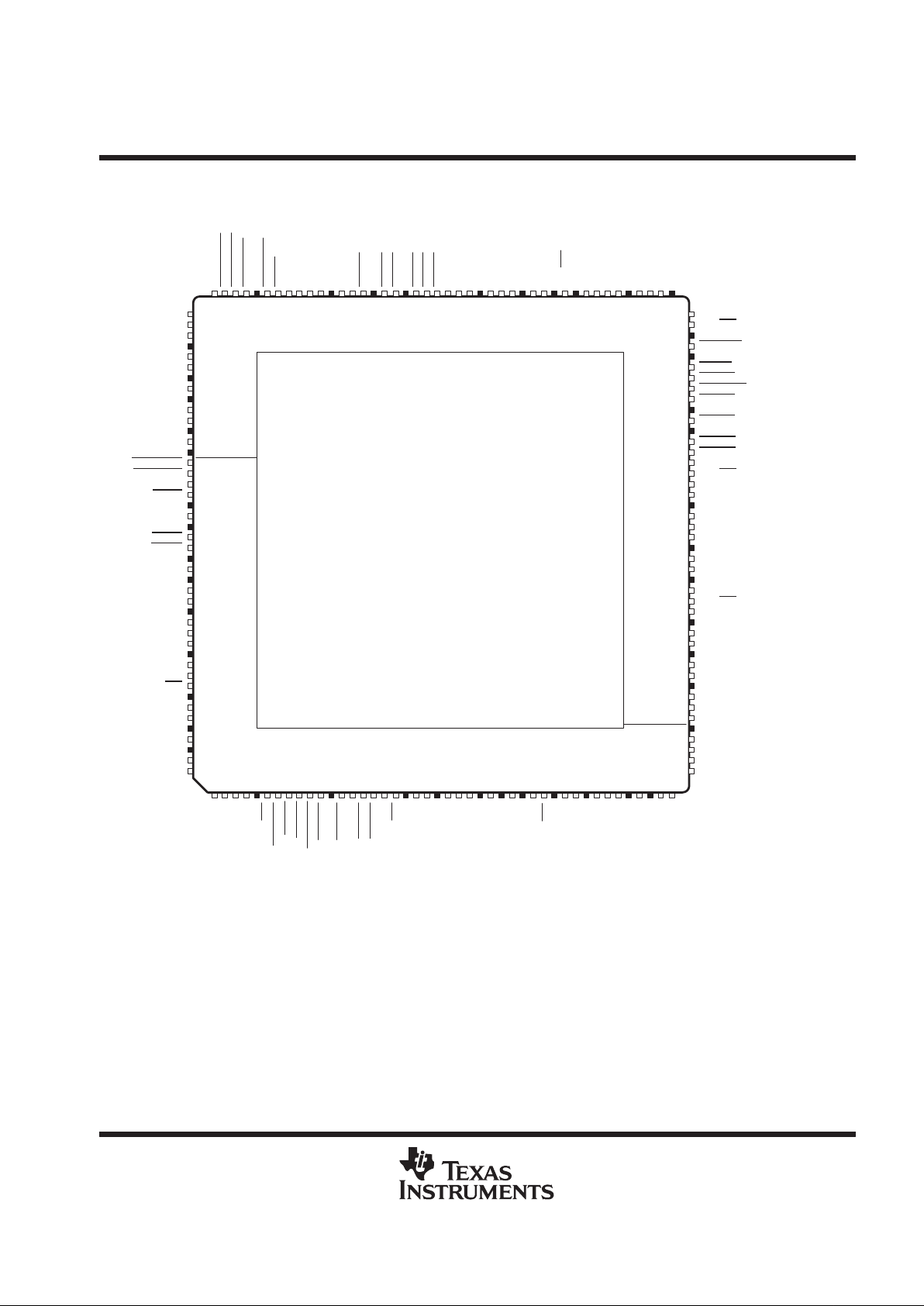
terminal assignments
P_C/BE2
P_FRAME
S_GPIO1
S_GPIO2
S_GPIO3
GND
S_PCLK0
S_PCLK1
V
CC
S_PCLK2
S_V
CCP
S_PCLK3
S_PCLK4
V
CC
S_PCLK5
GND
RST_MODE
P_CLKRUN
P_V
CCP
P_RST
GND
P_PCLK
V
CC
P_GNT
P_REQ
P_V
CCP
P_AD31
V
CC
P_AD30
P_AD29
GND
P_AD28
P_AD27
P_AD26
GND
P_AD25
P_AD24
P_C/BE3
GND
P_IDSEL
P_AD23
V
CC
P_AD22
P_V
CCP
P_AD21
P_AD20
133
134
135
136
137
138
139
140
141
142
143
144
145
146
147
148
149
150
151
152
153
154
155
156
157
158
159
160
161
162
163
164
165
166
167
168
169
170
171
172
173
174
175
176
21436587109121114131615181720192221242326252827302932313433363538374039424144
43
106
105
108
107
110
109
112
111
114
113
116
115
118
117
120
119
122
121
124
123
126
125
128
127
130
129
132
131
S_GPIO0
CC
88
87
86
85
84
83
82
81
80
79
78
77
76
75
74
73
72
71
70
69
68
67
66
65
64
63
62
61
60
59
58
57
56
55
54
53
52
51
50
49
48
47
46
45
S_AD16
S_C/BE2
GND
S_FRAME
V
CC
S_IRDY
S_TRDY
S_DEVSEL
S_STOP
S_V
CCP
S_LOCK
GND
S_PERR
S_SERR
S_PAR
S_C/BE1
S_AD15
S_AD14
V
CC
S_AD13
S_AD12
S_AD11
V
CC
S_AD10
S_AD9
GND
S_AD8
S_C/BE0
S_AD7
S_V
CCP
S_AD6
S_AD5
V
CC
S_AD4
S_AD3
GND
S_AD2
S_AD1
S_AD0
GND
P_GPIO0
P_GPIO1
P_GPIO2
P_GPIO3
919392
95
949796
99
98
101
100
103
102
104
89
90
V
S_FLSHREQ
S_FLSHACK
S_EXTARB
S_CLKRUN
S_RST
S_GNT5
S_GNT4
S_AD23
S_AD22
S_AD21
S_AD20
GND
S_AD19
S_AD18
S_AD17
S_AD28
S_AD27
S_AD26
GND
S_AD25
S_AD24
S_C/BE3
S_REQ3
S_REQ2
S_REQ1
S_REQ0
S_AD31
S_AD30
S_AD29
GND
S_REQ5
S_REQ4
S_GNT3
S_GNT2
GND
CC
V
S_GNT0
S_GNT1
CCP
S_V
CC
V
CCP
S_V
CC
V
P_AD19
P_AD18
P_AD17
P_AD16
GND
P_IRDY
P_TRDY
P_DEVSEL
P_STOP
V
P_LOCK
P_V
P_PERR
P_SERR
P_PAR
P_C/BE1
GND
P_AD15
P_AD14
GND
P_AD13
P_AD12
P_AD11
P_AD10
P_AD9
GND
P_AD8
P_C/BE0
GND
P_AD7
P_AD6
P_AD5
P_AD4
P_AD3
P_AD2
P_AD1
P_AD0
CC
CCP
V
CC
P_V
CCP
V
CC
V
CC
P_V
CCP
PGF PACKAGE
(TOP VIEW)
PCI2031
Secondary
Primary

PCI2031
PCI-TO-PCI BRIDGE
SCPS017A – DECEMBER 1997 – REVISED JANUARY 1998
4
POST OFFICE BOX 655303 • DALLAS, TEXAS 75265
Table 1. Signal Names Sorted by Terminal Number
NO. SIGNAL NAME NO. SIGNAL NAME NO. SIGNAL NAME NO. SIGNAL NAME
1 P_AD19 45 P_GPIO3 89 V
CC
133 S_GPIO1
2 P_AD18 46 P_GPIO2 90 S_AD17 134 S_GPIO2
3 P_AD17 47 P_GPIO1 91 S_AD18 135 S_GPIO3
4 P_AD16 48 P_GPIO0 92 S_AD19 136 GND
5 GND 49 GND 93 GND 137 S_PCLK0
6 P_C/BE2 50 S_AD0 94 S_AD20 138 S_PCLK1
7 P_FRAME 51 S_AD1 95 S_AD21 139 V
CC
8 P_IRDY 52 S_AD2 96 S_AD22 140 S_PCLK2
9 P_TRDY 53 GND 97 S_AD23 141 S_V
CCP
10 P_DEVSEL 54 S_AD3 98 S_V
CCP
142 S_PCLK3
11 P_STOP 55 S_AD4 99 S_C/BE3 143 S_PCLK4
12 V
CC
56 V
CC
100 V
CC
144 V
CC
13 P_LOCK 57 S_AD5 101 S_AD24 145 S_PCLK5
14 P_V
CCP
58 S_AD6 102 S_AD25 146 GND
15 P_PERR 59 S_V
CCP
103 GND 147 RST_MODE
16 P_SERR 60 S_AD7 104 S_AD26 148 P_CLKRUN
17 P_PAR 61 S_C/BE0 105 S_AD27 149 P_V
CCP
18 P_C/BE1 62 S_AD8 106 S_AD28 150 P_RST
19 GND 63 GND 107 GND 151 GND
20 P_AD15 64 S_AD9 108 S_AD29 152 P_PCLK
21 P_AD14 65 S_AD10 109 S_AD30 153 V
CC
22 GND 66 V
CC
110 S_AD31 154 P_GNT
23 P_AD13 67 S_AD11 111 S_REQ0 155 P_REQ
24 P_AD12 68 S_AD12 112 S_REQ1 156 P_V
CCP
25 P_AD11 69 S_AD13 113 S_REQ2 157 P_AD31
26 V
CC
70 V
CC
114 V
CC
158 V
CC
27 P_AD10 71 S_AD14 115 S_REQ3 159 P_AD30
28 P_V
CCP
72 S_AD15 116 S_REQ4 160 P_AD29
29 P_AD9 73 S_C/BE1 117 S_V
CCP
161 GND
30 GND 74 S_PAR 118 S_REQ5 162 P_AD28
31 P_AD8 75 S_SERR 119 S_GNT0 163 P_AD27
32 P_C/BE0 76 S_PERR 120 S_GNT1 164 P_AD26
33 GND 77 GND 121 GND 165 GND
34 P_AD7 78 S_LOCK 122 S_GNT2 166 P_AD25
35 P_AD6 79 S_VCCP 123 S_GNT3 167 P_AD24
36 V
CC
80 S_STOP 124 S_GNT4 168 P_C/BE3
37 P_AD5 81 S_DEVSEL 125 S_GNT5 169 GND
38 P_AD4 82 S_TRDY 126 S_RST 170 P_IDSEL
39 P_AD3 83 S_IRDY 127 S_CLKRUN 171 P_AD23
40 V
CC
84 V
CC
128 V
CC
172 V
CC
41 P_AD2 85 S_FRAME 129 S_EXTARB 173 P_AD22
42 P_VCCP 86 GND 130 S_FLSHACK 174 P_V
CCP
43 P_AD1 87 S_C/BE2 131 S_FLSHREQ 175 P_AD21
44 P_AD00 88 S_AD16 132 S_GPIO0 176 P_AD20

PCI2031
PCI-TO-PCI BRIDGE
SCPS017A – DECEMBER 1997 – REVISED JANUARY 1998
5
POST OFFICE BOX 655303 • DALLAS, TEXAS 75265
Terminal Functions
primary PCI system
TERMINAL
I/O
NAME NO.
TYPE
FUNCTION
P_CLK 152 I
Primary PCI bus clock. P_CLK provides timing for all transactions on the primary PCI bus. All primary PCI signals
are sampled at rising edge of P_CLK.
P_RST
150 I
PCI reset. When the primary PCI bus reset is asserted, P_RST causes the bridge to 3-state all output buffers
and reset all internal registers. When asserted, the device is completely nonfunctional. During P_RST
, the
secondary interface is driven low. After P_RST
is deasserted, the bridge is in its default state.
primary PCI address and data
TERMINAL
I/O
NAME NO.
TYPE
FUNCTION
P_AD31
P_AD30
P_AD29
P_AD28
P_AD27
P_AD26
P_AD25
P_AD24
P_AD23
P_AD22
P_AD21
P_AD20
P_AD19
P_AD18
P_AD17
P_AD16
P_AD15
P_AD14
P_AD13
P_AD12
P_AD11
P_AD10
P_AD9
P_AD8
P_AD7
P_AD6
P_AD5
P_AD4
P_AD3
P_AD2
P_AD1
P_AD0
157
159
160
162
163
164
166
167
171
173
175
176
1
2
3
4
20
21
23
24
25
27
29
31
34
35
37
38
39
41
43
44
I/O
Primary address/data bus. These signals make up the multiplexed PCI address and data bus on the primary
interface. During the address phase of a primary bus PCI cycle, P_AD31–P_AD0 contain a 32-bit address
or other destination information. During the data phase, P_AD31–P_AD0 contain data.
P_C/BE3
P_C/BE2
P_C/BE1
P_C/BE0
168
6
18
32
I/O
Primary bus commands and byte enables. These signals are multiplexed on the same PCI terminals. During
the address phase of a primary bus PCI cycle, P_C/BE3
–P_C/BE0 define the bus command. During the
data phase, this 4-bit bus is used as byte enables. The byte enables determine which byte paths of the full
32-bit data bus carry meaningful data. P_C/BE0
applies to byte 0 (P_AD7–P_AD0), P_C/BE1 applies to
byte 1 (P_AD15–P_AD8), P_C/BE2
applies to byte 2 (P_AD23–P_AD16), and P_C/BE3 applies to byte 3
(P_AD31–P_AD24).
P_CLKRUN 148 I/O
Primary PCI bus clock run. P_CLKRUN is used by the central resource to request permission to stop the
PCI clock or to slow it down.

PCI2031
PCI-TO-PCI BRIDGE
SCPS017A – DECEMBER 1997 – REVISED JANUARY 1998
6
POST OFFICE BOX 655303 • DALLAS, TEXAS 75265
Terminal Functions (Continued)
primary PCI interface control
TERMINAL
I/O
NAME NO.
TYPE
FUNCTION
P_DEVSEL 10 I/O
Primary device select. The bridge asserts P_DEVSEL to claim a PCI cycle as the target device. As a PCI
initiator on the primary bus, the bridge monitors P_DEVSEL
until a target responds. If no target responds
before time-out occurs, then the bridge terminates the cycle with an initiator abort.
P_FRAME
7 I/O
Primary cycle frame. P_FRAME is driven by the initiator of a primary bus cycle. P_FRAME is asserted to
indicate that a bus transaction is beginning, and data transfers continue while this signal is asserted. When
P_FRAME
is deasserted, the primary bus transaction is in the final data phase.
P_GNT
154 I
Primary bus grant to bridge. P_GNT is driven by the primary PCI bus arbiter to grant the bridge access to the
primary PCI bus after the current data transaction has completed. P_GNT
may or may not follow a primary
bus request, depending on the primary bus parking algorithm.
P_GPIO0
P_GPIO1
P_GPIO2
P_GPIO3
48
47
46
45
I/O
Primary bus general-purpose I/O terminals. These terminals are provided for general input/output use in
system design.
P_IDSEL 170 I
Initialization device select. P_IDSEL selects the bridge during configuration space accesses. P_IDSEL can
be connected to one of the upper 24 PCI address lines on the primary PCI bus.
Note: There is no IDSEL signal interfacing the secondary PCI bus; thus, the entire configuration space of the
bridge can only be accessed from the primary bus.
P_IRDY 8 I/O
Primary initiator ready. P_IRDY indicates the primary bus initiator’s ability to complete the current data phase
of the transaction. A data phase is completed on a rising edge of P_CLK where both P_IRDY
and P_TRDY
are asserted. Until P_IRDY and P_TRDY are both sampled asserted, wait states are inserted.
P_LOCK 13 I/O Primary PCI bus lock. P_LOCK is used to lock the primary bus and gain exclusive access as an initiator.
P_PAR 17 I/O
Primary parity. In all primary bus read and write cycles, the bridge calculates even parity across the P_AD
and P_C/BE
buses. As an initiator during PCI write cycles, the bridge outputs this parity indicator with a
one-P_CLK delay . As a target during PCI read cycles, the calculated parity is compared to the initiator’s parity
indicator; a misdemeanor can result in a parity error assertion (P_PERR
).
P_PERR
15 I/O
Primary parity error indicator. P_PERR is driven by a primary bus PCI device to indicate that calculated parity
does not match P_PAR when P_PERR
is enabled through bit 6 of the command register.
P_REQ 155 O
Primary PCI bus request. P_REQ is asserted by the bridge to request access to the primary PCI bus as an
initiator.
P_SERR 16 O
Primary system error. Output pulsed from the bridge when enabled through the command register indicating
a system error has occurred. The bridge need not be the target of the primary PCI cycle to assert P_SERR
.
When bit 6 is enabled in the bridge control register, P_SERR
pulses, indicating that a system error has
occurred on one of the subordinate buses downstream from the bridge.
P_STOP 11 I/O
Primary cycle stop signal. P_STOP is driven by a PCI target to request the initiator to stop the current primary
bus transaction. P_STOP
is used for target disconnects and is commonly asserted by target devices that do
not support burst data transfers.
RST_MODE
147 I
If RST_MODE is asserted during P_RST, it causes S_RST to be asserted and the secondary clocks to be
turned off.
P_TRDY 9 I/O
Primary target ready. P_TRDY indicates the primary bus target’s ability to complete the current data phase
of the transaction. A data phase is completed on a rising edge of P_CLK where both P_IRDY
and P_TRDY
are asserted. Until both P_IRDY and P_TRDY are asserted, wait states are inserted.

PCI2031
PCI-TO-PCI BRIDGE
SCPS017A – DECEMBER 1997 – REVISED JANUARY 1998
7
POST OFFICE BOX 655303 • DALLAS, TEXAS 75265
Terminal Functions (Continued)
secondary PCI system
TERMINAL
I/O
NAME NO.
TYPE
FUNCTION
S_PCLK5
S_PCLK4
S_PCLK3
S_PCLK2
S_PCLK1
S_PCLK0
145
143
142
140
138
137
O
Secondary PCI bus clock. Provides timing for all transactions on the secondary PCI bus. All secondary PCI
signals are sampled at the rising edge of S_CLK5–S_CLK0.
S_CLKRUN
127 I/O
Secondary PCI bus clock run. S_CLKRUN is output by the bridge to indicate that S_PCLKn is to be stopped.
S_CLKRUN
is driven by secondary bus PCI devices to request that S_PCLKn be stopped.
S_EXTARB 129 I
Secondary external arbiter enable. When S_EXTARB is asserted, the secondary external arbiter is enabled.
When the external arbiter is enabled, S_REQ0
is reconfigured as a secondary bus grant input to the bridge
and S_GNT0
is reconfigured as a secondary bus master request to the external arbiter on the secondary bus.
S_RST 126 O
Secondary PCI reset. S_RST is a logical OR of P_RST and the state of the secondary bus reset bit of the
bridge control register. S_RST
is asynchronous with respect to the state of the secondary interface CLK
signal.

PCI2031
PCI-TO-PCI BRIDGE
SCPS017A – DECEMBER 1997 – REVISED JANUARY 1998
8
POST OFFICE BOX 655303 • DALLAS, TEXAS 75265
Terminal Functions (Continued)
secondary PCI address and data
TERMINAL
I/O
NAME NO.
TYPE
FUNCTION
S_AD31
S_AD30
S_AD29
S_AD28
S_AD27
S_AD26
S_AD25
S_AD24
S_AD23
S_AD22
S_AD21
S_AD20
S_AD19
S_AD18
S_AD17
S_AD16
S_AD15
S_AD14
S_AD13
S_AD12
S_AD11
S_AD10
S_AD9
S_AD8
S_AD7
S_AD6
S_AD5
S_AD4
S_AD3
S_AD2
S_AD1
S_AD0
110
109
108
106
105
104
102
101
97
96
95
94
92
91
90
88
72
71
69
68
67
65
64
62
60
58
57
55
54
52
51
50
I/O
Secondary address/data bus. These signals make up the multiplexed PCI address and data bus on the
secondary interface. During the address phase of a secondary bus PCI cycle, S_AD31–S_AD0 contain a
32-bit address or other destination information. During the data phase, S_AD31–S_AD0 contain data.
S_C/BE3
S_C/BE2
S_C/BE1
S_C/BE0
99
87
73
61
I/O
Secondary bus commands and byte enables. These signals are multiplexed on the same PCI terminals.
During the address phase of a secondary bus PCI cycle, S_C/BE3
–S_C/BE0 define the bus command.
During the data phase, this 4-bit bus is used as byte enables. The byte enables determine which byte paths
of the full 32-bit data bus carry meaningful data. S_C/BE0
applies to byte 0 (S_AD7–S_AD0), S_C/BE1
applies to byte 1 (S_AD15–S_AD8), S_C/BE2 applies to byte 2 (S_AD23–S_AD16), and S_C/BE3 applies
to byte 3 (S_AD31–S_AD24).
S_DEVSEL 81 I/O
Secondary device select. The bridge asserts S_DEVSEL to claim a PCI cycle as the target device. As a PCI
initiator on the secondary bus, the bridge monitors S_DEVSEL
until a target responds. If no target responds
before timeout occurs, then the bridge terminates the cycle with an initiator abort.
S_FRAME 85 I/O
Secondary cycle frame. S_FRAME is driven by the initiator of a secondary bus cycle. S_FRAME is asserted
to indicate that a bus transaction is beginning and data transfers continue while S_FRAME
is asserted. When
S_FRAME
is deasserted, the secondary bus transaction is in the final data phase.
S_GNT5
S_GNT4
S_GNT3
S_GNT2
S_GNT1
S_GNT0
125
124
123
122
120
119
O
Secondary bus grant to the bridge. The bridge provides internal arbitration and these signals are used to grant
potential secondary PCI bus masters access to the bus. Seven potential initiators (including the bridge) can
be located on the secondary PCI bus.
When the internal arbiter is disabled, S_GNT0
is reconfigured as an external secondary bus request signal
for the bridge.

PCI2031
PCI-TO-PCI BRIDGE
SCPS017A – DECEMBER 1997 – REVISED JANUARY 1998
9
POST OFFICE BOX 655303 • DALLAS, TEXAS 75265
Terminal Functions (Continued)
secondary PCI interface control
TERMINAL
I/O
NAME NO.
TYPE
FUNCTION
S_GPIO0
S_GPIO1
S_GPIO2
S_GPIO3
132
133
134
135
I/O
Secondary general-purpose I/O terminals. These terminals are provided for general-purpose input/output
use in system design.
S_IRDY 83 I/O
Secondary initiator ready. S_IRDY indicates the secondary bus initiator’s ability to complete the current data
phase of the transaction. A data phase is completed on a rising edge of S_PCLKn where both S_IRDY
and
S_TRDY
are asserted; until S_IRDY and S_TRDY are asserted, wait states are inserted.
S_LOCK 78 I/O Secondary lock S_LOCK is used to lock the secondary bus and gain exclusive access as an initiator.
S_PAR 74 I/O
Secondary parity. In all secondary bus read and write cycles, the bridge calculates even parity across the
S_AD and S_C/BE
buses. As an initiator during PCI write cycles, the bridge outputs this parity indicator with
a one-S_PCLKn delay . As a target during PCI read cycles, the calculated parity is compared to the initiator’s
parity indicator. A miscompare can result in a parity error assertion (S_PERR
).
S_PERR
76 I/O
Secondary parity error indicator. S_PERR is driven by a secondary bus PCI device to indicate that
calculated parity does not match S_PAR when enabled through the command register.
S_REQ5
S_REQ4
S_REQ3
S_REQ2
S_REQ1
S_REQ0
118
116
115
113
112
111
I
Secondary PCI bus request signals. The bridge provides internal arbitration, and these signals are used as
inputs from secondary PCI bus initiators requesting the bus. Seven potential initiators (including the bridge)
can be located on the secondary PCI bus.
S_REQ0
111
When the internal arbiter is disabled, S_REQ0 is reconfigured as an external secondary bus grant for the
bridge.
S_SERR
75 I
Secondary system error. S_SERR is passed through the primary interface by the bridge if enabled through
the bridge control register. S_SERR
is never asserted by the bridge.
S_STOP 80 I/O
Secondary cycle stop signal. S_STOP is driven by a PCI target to request the initiator to stop the current
secondary bus transaction. S_STOP
is used for target disconnects and is commonly asserted by target
devices that do not support burst data transfers.
S_TRDY 82 I/O
Secondary target ready. S_TRDY indicates the secondary bus target’s ability to complete the current data
phase of the transaction. A data phase is completed on a rising edge of S_PCLKn where both S_IRDY
and
S_TRDY
are asserted; until S_IRDY and S_TRDY are asserted, wait states are inserted.
S_FLSHREQ 131 I
Flush request. When S_FLSHREQ is asserted, it signals a request to the PCI2031 to suspend internal write
posting. When the bridge is ready to suspend internal write posting, it responds by asserting S_FLSHACK
.
S_FLSHACK
remains asserted until the write posting buffers are empty.
S_FLSHACK
130 O
Flush acknowledge. S_FLSHACK is asserted by the PCI2031 to indicate that the internal write posting is
suspended. S_FLSHACK
remains asserted until the write posting buffers are empty.
power supply
TERMINAL
NAME NO.
FUNCTION
GND
5, 19, 22, 30, 33, 49, 53, 63, 77, 86, 93, 103,
107, 121, 136, 146, 151, 161, 165, 169
Device ground terminals
V
CC
12, 26, 36, 40, 56, 66, 70, 84, 89, 100, 114,
128, 139, 144, 153, 158, 172
Power-supply terminal for core logic (3.3 V)
P_V
CCP
14, 28, 42, 149, 156, 174
Primary bus-signaling environment supply. P_V
CCP
is used in protection circuitry
on primary bus I/O signals.
S_V
CCP
59, 79, 98, 117, 141
Secondary bus-signaling environment supply. S_V
CCP
is used in protection
circuitry on primary bus I/O signals.

PCI2031
PCI-TO-PCI BRIDGE
SCPS017A – DECEMBER 1997 – REVISED JANUARY 1998
10
POST OFFICE BOX 655303 • DALLAS, TEXAS 75265
architecture
This section provides an overview of the PCI2031 PCI-to-PCI bridge features and functionality. Detailed
descriptions of the bridge’s internal registers and extension registers are also provided.
introduction to the PCI2031
The PCI2031 is a bridge between two PCI buses, and is compliant with both the PCI Local Bus Specification 2.1
and the PCI-to-PCI Bridge Specification 1.0. The bridge supports two 32-bit PCI buses operating at a maximum
of 33 MHz. The primary and secondary buses operate independently in either a 3.3-V or 5-V signaling
environment. The core logic of the bridge, however, is powered at 3.3 V to reduce power consumption.
Host software interacts with the bridge through internal registers. These internal registers provide the standard
PCI status and control for both the primary and secondary buses. There are many vendor-specific features
included in the bridge that exist in the TI extension register set. The PCI configuration header of the bridge is
only accessible from the primary PCI interface.
The bridge provides internal arbitration for the six possible secondary bus masters, and provides each with a
dedicated active low request/grant pair (REQ
/GNT). The arbiter features a two-tier rotational scheme with the
PCI2031 bridge defaulting to the highest priority tier. The bus parking scheme is also configurable and can be
set to either park grant (GNT) on the bridge or on the last mastering device.
Upon system power up, power-on self-test (POST) software configures the bridge according to the devices that
exist on subordinate buses, and enables performance-enhancing features of the PCI2031. In a typical system,
this is the only communication with the bridge’s internal register set.
serial EEPROM interface
The PCI2031 uses a serial EEPROM interface for loading the bridge’s subsystem vendor ID register and
subsystem ID register from an EEPROM after a reset on the primary bus. This interface also loads the slot
number register, the device mask register , and the device-type register after a primary reset. The PCI2031 can
trap accesses to the subsystem vendor ID register and subsystem ID register of devices sitting on its secondary
bus, based on the settings of these two registers.
While the EEPROM is loading data into the PCI2031 subsystem vendor ID register and slot number register,
all configuration read accesses to these registers are retried. All configuration reads to registers 2Ch and 40h
of devices (0–7) behind the bridge are also retried. The interface uses general-purpose I/O terminals S_GPIO0
for the clock and S_GPIO1 for data.
The device-type register represents up to six devices on the secondary bus of the PCI2031. Each bit in this
register corresponds to one device. During the address phase of a type 1 configuration cycle, if the value of bit
0 of the device-type register is 1, it implies that the device corresponding to device number 00000 (see bits
AD15–AD1 1 in Figure 2 on page 13) is a CardBus controller. If the value of bit 0 is 0, it indicates that the device
is a standard PCI device. Bit 1 in the device-type register corresponds to device number 00001, bit 2
corresponds to device number 00010, bit 3 corresponds to device number 00011, and so on.
The device-type and device mask registers control configuration read accesses to a device’s subsystem vendor
ID register. See
device mask register
and
device-type register
.

PCI2031
PCI-TO-PCI BRIDGE
SCPS017A – DECEMBER 1997 – REVISED JANUARY 1998
11
POST OFFICE BOX 655303 • DALLAS, TEXAS 75265
The PCI2031 reads data from the serial EEPROM starting at address 00000000. The slave address of the serial
EEPROM must be at 10100000 for the PCI2031 to see it. The PCI2031 then reads seven bytes of data from
the EEPROM. The PCI2031 reads the data in the following order:
1. High byte of the subsystem ID
2. Low byte of the subsystem ID
3. High byte of the subsystem vendor ID.
4. Low byte of the subsystem vendor ID
5. Device mask
6. Device type
7. Slot number
The only register that is not programmed in the serial EEPROM is the chassis number register.

PCI2031
PCI-TO-PCI BRIDGE
SCPS017A – DECEMBER 1997 – REVISED JANUARY 1998
12
POST OFFICE BOX 655303 • DALLAS, TEXAS 75265
PCI commands
The bridge responds as a PCI target device to PCI bus cycles based on the decoding of each address phase
and internal register settings. Table 2 lists the valid PCI bus cycles and their encoding on the command/byte
enables (C/BE) bus during the address phase of a bus cycle.
Table 2. PCI Command Definition
C/BE3–C/BE0
COMMAND
0000 Interrupt acknowledge
0001 Special cycle
0010 I/O read
0011 I/O write
0100 Reserved
0101 Reserved
0110 Memory read
0111 Memory write
1000 Reserved
1001 Reserved
1010 Configuration read
1011 Configuration write
1100 Memory read multiple
1101 Dual address cycle
1110 Memory read line
1111 Memory write and invalidate
The bridge never responds as a PCI target to the interrupt acknowledge, special cycle, dual address cycle, or
reserved commands. The bridge does, however, initiate special cycles on both interfaces when a type 1
configuration cycle issues the special cycle request. The remaining PCI commands address either memory , I/O,
or configuration space. The bridge accepts PCI cycles by asserting DEVSEL
as a medium-speed device, i.e.,
DEVSEL is asserted two clock cycles after the address phase.
configuration cycles
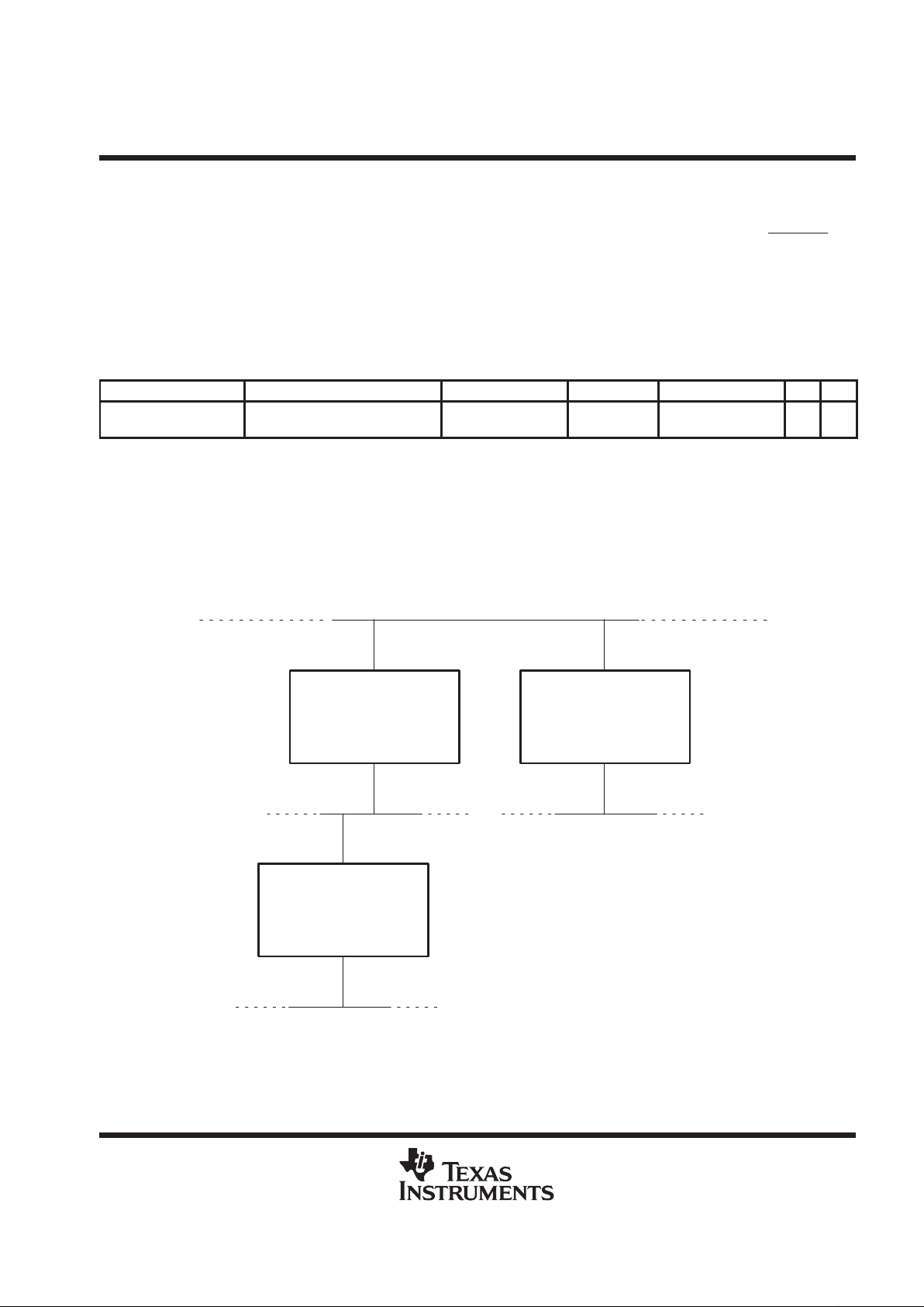
PCI Local Bus Specification 2.1 defines two types of PCI configuration read and write cycles: type 0 and type 1.
The bridge decodes each type differently . Type 0 configuration cycles are intended for devices on the primary
bus, while type 1 configuration cycles are intended for devices at some hierarchically subordinate bus. The
difference between these two types of cycles is the encoding of the primary PCI (P_AD) bus during the address
phase of the cycle. The P_AD bus encoding during the address phase of a type 0 configuration cycle is shown
in Figure 1. The 6-bit register number field represents an 8-bit address with the two lower bits masked to 0,
indicating a double-word boundary. This results in a 256-byte configuration address space per function per
device. Individual byte accesses may be selected within a word by using the P_C/BE
signals during the data
phase of the cycle.
31 11 10 8 721 0
Reserved
Function
number
Register
number
0 0
Figure 1. PCI AD31–AD0 During Address Phase of a Type 0 Configuration Cycle
PCI2031
PCI-TO-PCI BRIDGE
SCPS017A – DECEMBER 1997 – REVISED JANUARY 1998
13
POST OFFICE BOX 655303 • DALLAS, TEXAS 75265
configuration cycles (continued)
The bridge claims only type 0 configuration cycles when its P_IDSEL terminal is asserted during the address
phase of the cycle and the PCI function number encoded in the cycle is 0. If the function number is 1 or greater,
the bridge does not recognize the configuration command. In this case, the bridge does not assert DEVSEL and
the configuration transaction results in a master abort. The bridge services valid type 0 configuration read or
write cycles by accessing internal registers from the configuration header (see Table 3).
Because type 1 configuration cycles are issued to devices on subordinate buses, the bridge claims type 1 cycles
based on the bus number of the destination bus. The P_AD bus encoding during the address phase of a type 1
cycle is shown in Figure 2. The device number and bus number fields define the destination bus and device for
the cycle.
31 24 23 16 15 11 10 8 721 0
Reserved Bus number
Device
number
Function
number
Register
number
0 1
Figure 2. PCI AD31–AD0 During Address Phase of a Type 1 Configuration Cycle
Several bridge configuration registers shown in Table 3 are significant when decoding and claiming type 1
configuration cycles. The destination bus number encoded on the P_AD bus is compared to the values
programmed in the bridge configuration registers 18h, 19h, and 1Ah, which are the primary bus number,
secondary bus number, and subordinate bus number registers, respectively . These registers default to 00h and
are programmed by host software to reflect the bus hierarchy in the system (seeFigure 3 for an example of a
system bus hierarchy and how the PCI2031 bus number registers would be programmed in this case).
PCI Bus 0
Primary Bus 00h
Secondary Bus 01h
Subordinate Bus 02h
PCI2031
Primary Bus 00h
Secondary Bus 03h
Subordinate Bus 03h
PCI2031
PCI Bus 1 PCI Bus 3
Primary Bus 01h
Secondary Bus 02h
Subordinate Bus 02h
PCI2031
PCI Bus 2
Figure 3. Bus Hierarchy and Numbering

PCI2031
PCI-TO-PCI BRIDGE
SCPS017A – DECEMBER 1997 – REVISED JANUARY 1998
14
POST OFFICE BOX 655303 • DALLAS, TEXAS 75265
special cycle generation
The bridge is designed to generate special cycles on both buses through a type 1 cycle conversion. During a
type 1 configuration cycle, if the bus number field matches the bridge’s secondary bus number, the device
number field is 1Fh, and the function number field is 07h, the bridge generates a special cycle on the secondary
bus with a message that matches the type 1 configuration cycle data. If the bus number is a subordinate bus
and not the secondary, then the bridge passes the type 1 special cycle request through to the secondary
interface along with the proper message.
Special cycles are never passed through the bridge. Type 1 configuration cycles with a special cycle request
can propagate in both directions.
PCI Local Bus Specification 2.1 compliance
The most significant additions to the PCI Local Bus Specification 2.1 are the latency requirements placed on
PCI peripherals. Minimum response times are specified for a PCI device to respond with valid data. These
requirements are intended to improve throughput and reduce latencies on the PCI bus. The PCI2031 bridge
is fully compliant with these guidelines.
Other additions to revision 2.1 of the PCI specification include the subsystem ID and subsystem vendor ID
registers in the PCI configuration header. The PCI2031 bridge includes these features, as well.
PCI clock run feature
The PCI2031 supports the PCI clock run protocol as defined in the PCI Mobile Design Guide, Revision 1.0.
When the system’s central resource signals to the system that it wants to stop the PCI clock (PCLK) by driving
the primary clock run (P_CLKRUN
) signal high, the bridge either signals that it is OK to stop the PCI clock by
leaving P_CLKRUN deasserted (high), or signals to the system to keep the clock running by driving
P_CLKRUN low.
The PCI2031 clock run control register provides a clock run enable bit for the primary bus and a separate clock
run enable bit for the secondary bus. The bridge’s P_CLKRUN and secondary clock run (S_CLKRUN) feature
are enabled by setting bits 3 and 1, respectively , in the clock run control register. Bit 2 of the clock run control
register allows software to enable the bridge’s keep clock running mode to prevent the system from stopping
the PCI clock. There are two conditions for restarting the secondary clock: a downstream transaction restarts
the secondary clock; on the secondary, if S_CLKRUN is asserted, the secondary clock is restarted.
There are two clock run modes supported on the secondary bus. The bridge can be configured to stop the
secondary PCI clock only in response to a request from the primary bus to stop the clock, or it can be configured
to stop the secondary clock whenever the secondary bus is idle and there are no transaction requests from the
primary bus, regardless of the primary clock (see
clock run control register).
bus arbitration
The PCI2031 implements bus request (P_REQ) and bus grant (P_GNT) terminals for primary PCI bus
arbitration. Six secondary bus requests and six secondary bus grants are provided on the secondary of the
PCI2031. Seven potential initiators, including the bridge, can be located on the secondary bus. The PCI2031
provides a two-tier arbitration scheme on the secondary bus for priority bus-master handling.
The two-tier arbitration scheme improves performance in systems in which master devices do not all require
the same bandwidth. Any master that requires frequent use of the bus can be programmed to be in the higher
priority tier.
primary bus arbitration
The PCI2031, acting as an initiator on the primary bus, asserts P_REQ when forwarding transactions upstream
to the primary bus. In the upstream direction, as long as a posted write data or a delayed transaction request
is in the queue, the PCI2031 keeps P_REQ asserted. If a target disconnect, a target retry , or a target abort is
received in response to a transaction initiated on the primary bus by the PCI2031, the device deasserts P_REQ
for two PCI clock cycles.

PCI2031
PCI-TO-PCI BRIDGE
SCPS017A – DECEMBER 1997 – REVISED JANUARY 1998
15
POST OFFICE BOX 655303 • DALLAS, TEXAS 75265
primary bus arbitration (continued)
When the primary bus arbiter asserts P_GNT in response to a P_REQ from the PCI2031, the device initiates
a transaction on the primary bus during the next PCI clock cycle.
When P_REQ is not asserted and the primary bus arbiter asserts P_GNT to the PCI2031, the device responds
by parking the P_AD31–P_AD0 bus, the C/BE
3–C/BE0 bus, and primary parity (P_P AR) by driving them to valid
logic levels. If the PCI2031 is parking the primary bus and wants to initiate a transaction on the primary , it can
start the transaction on the next PCI clock by asserting the primary cycle frame (P_FRAME) while P_GNT is
still asserted. If P_GNT is deasserted, the bridge must rearbitrate for the bus to initiate a transaction.
internal secondary bus arbitration
Bit 6 of the secondary clock/arbiter disable register at configuration offset 6Ch controls the state of the internal
secondary arbiter. By default, the PCI2031 internal secondary bus arbiter is enabled (bit 6 is 0). The internal
arbiter can be disabled by setting bit 6 to 1. The PCI2031 provides six secondary bus request terminals and six
secondary bus grant terminals. Including the bridge itself, there are a total of seven potential secondary bus
masters. These request and grant signals are connected to the internal arbiter. When an external arbiter is
implemented, S_REQ5
–S_REQ1 and S_GNT5–S_GNT1 are 3-stated.
external secondary bus arbitration
An external secondary bus arbiter can be used instead of the PCI2031 internal bus arbiter. When using an
external arbiter, the PCI2031 internal arbiter should be disabled either by using the secondary external arbiter
enable (S_EXT ARB
) input, or by setting bit 6 of the secondary clock/arbiter disable register (at offset 6Ch) to 1.
When an external secondary bus arbiter is used, the PCI2031 internally reconfigures the S_REQ0
and S_GNT0
signals so that S_REQ0 becomes the secondary bus master grant for the bridge and S_GNT0 becomes the
secondary bus master request for the PCI2031. This is done because S_REQ0 is an input and can thus be used
to provide the grant input to the bridge, and S_GNT0 is an output and can thus provide the request output from
the bridge.
When an external arbiter is used, all unused secondary bus grant outputs (S_GNT5–S_GNT1) are 3-stated.
Any unused secondary bus request inputs (S_REQ5–S_REQ1) should be pulled high to prevent the inputs
from oscillating.
decode options
The PCI2031 supports positive, subtractive, and negative decoding. Positive decoding is a method of address
decoding in which a device responds only to accesses within an assigned address range. Negative decoding
is a method of address decoding in which a device responds only to accesses outside of an assigned address
range. Subtractive decoding is a method of address decoding in which a device responds to accesses not
claimed by any other devices on the bus. Subtractive decoding can be enabled on the primary bus or the
secondary bus.
extension windows with programmable decoding
The PCI2031 provides two programmable 32-bit extension windows. Each window can be programmed to be
a prefetchable memory window, a nonprefetchable memory window, or an I/O window. The TI extension
memory windows have a 4K-byte granularity, and the I/O windows have a double-word granularity. These
extension windows can be positively decoded either on the primary bus or on the secondary bus.
The standard PCI-to-PCI bridge memory and I/O windows specified by the PCI-to-PCI Bridge Specification 1.0
have a 1M-byte and 4K-byte granularity, respectively (see
memory base register
and
I/O base register
). The
TI extension windows provide smaller granularity for memory and I/O windows. The extension windows’
granularity matches the requirements of CardBus card windows, which also have 4K-byte granularity for
memory windows and double-word granularity for I/O windows. When a CardBus I/O card is sitting behind the
bridge, the smaller double-word I/O window granularity with the extension windows allows a smaller I/O window
than the 4K-byte window with the standard I/O base and limit registers.

PCI2031
PCI-TO-PCI BRIDGE
SCPS017A – DECEMBER 1997 – REVISED JANUARY 1998
16
POST OFFICE BOX 655303 • DALLAS, TEXAS 75265
extension windows with programmable decoding (continued)
A common I/O base address for popular sound cards is 300h–303h. Using the TI extension windows and
configuring the base I/O address for 300h establishes a 4-byte I/O address window from 300h–303h for
communicating with the sound card. Using the bridge’s standard I/O base register requires a minimum 4K-byte
window of memory.
The extension windows can be excluded from the primary bus decoding, thus creating a hole in a primary
window address range.
system error handling
The PCI2031 can be configured to signal a system error (SERR) for a variety of conditions. The SERR control
and status registers, configuration offset 60h and 61h, respectively , provide individual SERR control/status bits
for each condition for which the bridge can signal SERR. These individual bits enable SERR reporting for both
downstream and upstream transactions.
With the exception of the master retry timeout and address parity errors, SERR is signaled on the primary bus
for the following conditions, only if the corresponding bit in the SERR control register is set and the SERR enable
bit in the command register (configuration offset 04h, bit 8) is set. The system error signal (bit 14) in the primary
status register is set whenever the PCI2031 signals SERR.
Whenever the PCI2031 signals SERR on the primary bus, bit 14 in its status register gets set. Whenever the
PCI2031 detects SERR on the secondary bus, bit 14 in the secondary status register gets set (see
status
register
and
secondary status register
).
arbiter timeout
If a master on the secondary bus does not start a transaction within 16 clock cycles after receiving the bus grant,
the arbiter times out and generates SERR. When the bridge signals SERR due to an arbiter timeout, bit 0 of
the SERR status register is set. This bit can be cleared by writing a 1.
parity error on posted writes
If bit 1 in the SERR control register is set, parity errors on the target bus can be passed back to the initiator bus
as SERRs, only if the error is not detected by the bridge. For example, if the bridge accepts a posted write
transaction and does not detect a parity error, but the target of the posted write does detect bad parity and
asserts PERR on the target bus, the bridge passes the parity error (PERR) back to the initiator side as SERR.
When this occurs, bit 1 of the SERR status register gets set. The status bit is cleared by writing a 1.
target abort on posted writes
If bit 2 of the SERR control register is set and the bridge gets a target abort during a posted write transaction,
it signals SERR on the initiator bus. As a result, bit 2 of the SERR status register gets set. The status bit is cleared
by writing a 1.
master abort on posted writes
If bit 3 of the SERR control register is set and a posted write transaction results in a master abort, the bridge
signals SERR on the initiator bus. As a result, bit 3 of the SERR status register gets set. The status bit is cleared
by writing a 1.
discard timeout on nonprefetchable reads
If bit 4 of the SERR control register is set and the bridge discard timer expires during a nonprefetchable read
transaction, the bridge signals SERR. As a result, bit 4 of the SERR status register gets set. The status bit is
cleared by writing a 1.

PCI2031
PCI-TO-PCI BRIDGE
SCPS017A – DECEMBER 1997 – REVISED JANUARY 1998
17
POST OFFICE BOX 655303 • DALLAS, TEXAS 75265
data parity errors when the PCI2031 is mastering
If bit 5 of the SERR control register is set, the PCI2031 signals SERR when it detects a parity error while it is
mastering the bus. As a result, bit 5 of the SERR status register gets set. The status bit is cleared by writing a 1.
This bit should be enabled only when the bridge is configured for fixing parity.
address parity errors
If the parity error response bit (bit 6) of the command register is set, the PCI2031 signals SERR on address parity
errors and target abort. As a result, bit 6 of the SERR status register gets set. The status bit is cleared by writing
a 1. There is no separate control bit in the SERR control register for reporting this error.
master retry timeout
If the PCI2031 is configured for master retry timeout (bit 15 in the diagnostic register is 1), the PCI2031 signals
SERR when it is mastering the bus and the master retry timer times out. As a result, bit 7 of the SERR status
register gets set. The status bit is cleared by writing a 1. There is no separate control bit in the SERR control
register for reporting this error.
secondary SERR
The PCI2031 passes SERR from the secondary bus to the primary bus if it is enabled for SERR response (bit 8
in the command register is 1), and bit 1 in the bridge control register (configuration offset 03eh) is set.
parity handling and parity error reporting
The PCI2031 can be configured to pass parity or provide parity via bit 14 of the diagnostic register. When this
bit is cleared to 0, the bridge is enabled for passing parity errors. Parity error passing is the default mode in the
bridge. Parity error passing is recommended only if devices in the system are capable of error recovery. The
following parity conditions result in the bridge signaling an error.
address parity error
If the parity error response bit (bit 6) in the command register is set, the PCI2031 signals SERR on address parity
errors and target abort transactions. As a result, bit 6 in the SERR status register is set. The status bit is cleared
by writing a 1.
data parity error
If the parity error response bit (bit 6) in the command register is set, the PCI2031 signals PERR when it receives
bad data. When the bridge detects bad parity, bit 15 (detected parity error) in the PCI status register is set.
If the bridge is configured to respond to parity errors via bit 6 in the command register, the data parity error
detected bit (bit 8 in the status register) is set when the bridge detects bad parity . The data parity error detected
bit is also set when the bridge, as a bus master, asserts PERR or detects PERR.
master and target abort handling
If the PCI2031 receives a target abort during a write burst, it signals target abort back on the initiator bus. If it
receives a target abort during a read burst, it provides all of the valid data on the initiator bus and disconnects.
Target aborts for posted and nonposted transactions are reported as specified in the PCI-to-PCI Bridge
Specification 1.0.
Master aborts for posted and nonposted transactions are reported as specified in the PCI-to-PCI Bridge
Specification 1.0. If a transaction is attempted on the primary bus after a secondary reset is asserted, the
PCI2031 follows the master abort mode bit setting (bit 5 in the bridge control register) for reporting errors.

PCI2031
PCI-TO-PCI BRIDGE
SCPS017A – DECEMBER 1997 – REVISED JANUARY 1998
18
POST OFFICE BOX 655303 • DALLAS, TEXAS 75265
serialized interrupts
The PCI2031 supports serialized IRQs for systems that support the serialized interrupt standard defined in the
Serialized IRQ Support for PCI Systems Specification 6.0. This specification defines IRQ support for two
PCI-to-PCI bridges connected serially. The specification states that PCI-to-PCI bridges must buffer the
serialized IRQ stream from the secondary PCI bus to the primary PCI bus. The PCI2031 serializer provides the
required buffering.
Bit 0 of the Serialized IRQ Support register (configuration offset 79h) must be set to enable serialized IRQ
support. This register also controls the number of start pulses and the number of data frames. The PCI2031
can be programmed to provide a start pulse of 4 clocks or 6 clocks and the number of IRQ/data frames is
programmable from 17 to 32.
The PCI2031 buffers IRQ data upstream and IRQ stop pulses downstream. In continuous mode, the PCI2031
initiates and completes a start on the secondary side when a start is initiated on the primary side. In quiet mode,
the PCI2031 completes a start initiated by an IRQSER device on its secondary side and also initiates a start
on the primary side.
After a power up or reset in a two-bridge system, both bridges must have IRQ support enabled (bit 0 of the
Serialized IRQ Support register) before any data streams are initiated by the host controller.
The serialized IRQ implementation uses the P_GPIO1 general purpose I/O pin for the primary IRQSER
signaling and the S–GPIO2 general purpose I/O pin for the secondary IRQSER signaling.
discard timer
The PCI2031 is free to discard the data or status of a delayed transaction that was completed with a delayed
transaction termination when a bus master has not repeated the request within 210 or 215 PCI clocks
(approximately 30 µs and 993 µs, respectively). PCI Local Bus Specification 2.1 recommends that a bridge wait
2
15
PCI clocks before discarding the transaction data or status.
The PCI2031 implements a discard timer for use in delayed transactions. After a delayed transaction is
completed on the destination bus, the bridge may discard it under two conditions. The first condition occurs
when a read transaction is made to a region of memory that the bridge knows is prefetchable, or the command
is a memory read line or a memory read multiple, implying that the memory region is prefetchable. The other
condition occurs when the master originating the transaction (either a read or a write, prefetchable or
nonprefetchable) has not retried the transaction within 2
10
or 215 clocks. The number of clocks is tracked by
a timer referred to as the discard timer. When the discard timer expires, the bridge is required to discard the data.
The PCI2031 default value for the discard timer is 215 clocks; however, this value can be set to 210 clocks by
clearing bit 1 in the diagnostic register (configuration offset 70h–71h). For more information on the discard timer ,
see
error conditions
in PCI Local Bus Specification 2.1.
delayed transactions
The bridge supports delayed transactions as defined in PCI Local Bus Specification 2.1. A target must be able
to complete the initial data phase in 16 PCI clocks or less from the assertion of the cycle frame (FRAME), and
subsequent data phases must complete in eight PCI clocks or less. A delayed transaction consists of
three phases:
D
An initiator device issues a request.
D
The target completes the request on the destination bus and signals the completion to the initiator.
D
The initiator completes the request on the originating bus.

PCI2031
PCI-TO-PCI BRIDGE
SCPS017A – DECEMBER 1997 – REVISED JANUARY 1998
19
POST OFFICE BOX 655303 • DALLAS, TEXAS 75265
delayed transactions (continued)
If the bridge is the target of a PCI transaction and it must access a slow device to write or read the requested
data, and the transaction takes longer than 16 clocks, the bridge must latch the address, the command, and
the byte enables, then issue a retry to the initiator. The initiator must end the transaction without any transfer
of data and is required to retry the transaction later using the same address, command, and byte enables. This
is the first phase of the delayed transaction.
During the second phase, if the transaction is a read cycle, the bridge fetches the requested data on the
destination bus, stores it internally, and obtains the completion status, thus completing the transaction on the
destination bus. If it is a write transaction, the bridge writes the data and obtains the completion status, thus
completing the transaction on the destination bus. The bridge stores the completion status until the master on
the initiating bus retries the initial request.
During the third phase, the initiator rearbitrates for the bus. When the bridge sees the initiator retry the
transaction, it compares the second request to the first request. If the address, command, and byte enables
match the values latched in the first request, the completion status (and data if the request was a read) is
transferred to the initiator. At this point, the delayed transaction is complete. If the second request from the
initiator does not match the first request exactly, the bridge issues another retry to the initiator.
When bit 2 of the diagnostic register is 0, the PCI2031 is configured for immediate retry mode. In immediate
retry mode, the bridge issues a retry immediately, instead of after 16 clocks, on delayed transactions.
flush request/flush acknowledge
The bridge implements two active-low signals on the secondary interface for write-posting buffer control. These
signals are secondary flush request (S_FLSHREQ
) and secondary flush acknowledge (S_FLSHACK).
S_FLSHREQ is an input to the secondary interface of the bridge to request that internal write posting, in both
directions, be disabled. When the bridge detects S_FLSHREQ is asserted, it responds with an S_FLSHACK
acknowledgment. S_FLSHACK remains asserted (low) until the write-posting buffers are empty.
general-purpose input/output terminals
The PCI2031 provides four primary and four secondary general-purpose input/output (I/O) terminals for design
flexibility. The general-purpose I/O terminals can be used for turning LEDs and other components on and off,
and switching power on and off for different planes in the system and other similar uses. For example:
D
P_GPIO0 can be configured as an output and used as an interrupt request from the PCI2031 when docking
support is enabled.
D
P_GPIO2 and P_GPIO3 can be configured as input pins and used as docking station support detect pins
1 and 2, respectively.
D
S_GPIO0 and S_GPIO1 are used for the serial EEPROM interface between the EEPROM and the
PCI2031. S_GPIO0 serves as the clock line and S_GPIO1 serves as the data line.
D
P_GPIO1 and S_GPIO2 can be used as primary and secondary bus IRQSER pins, respectively.
slot numbers and chassis numbers
The PCI2031 contains two registers, slot number and chassis number, which help in identifying the physical
location of various controller devices in a server-based system.
In a desktop computer, there are typically just a few PCI expansion slots. These slots usually host a graphics
controller, disk drive controller , and a network controller. Generally , there is no duplication of functionality among
the devices. It is relatively easy to connect the appropriate cables to the devices and to configure this type of
system during power on.

PCI2031
PCI-TO-PCI BRIDGE
SCPS017A – DECEMBER 1997 – REVISED JANUARY 1998
20
POST OFFICE BOX 655303 • DALLAS, TEXAS 75265
slot numbers and chassis numbers (continued)
In a network server system, where the server might have multiple connections to several storage subsystems
and LAN segments, identifying a particular device in the network can be difficult. A server might contain several
PCI expansion slots, some of which contain multiple controllers. In this case, it is more difficult to identify a
particular chassis and slot within the chassis that contains a specific controller. In such a server system, if a
controller fails, software must have a way to determine which device failed and communicate this to the system
administrator so it can be replaced.
At power on, the system configuration software assigns each subsystem cabinet a chassis number. The network
controllers (e.g., a PCI Ethernet controller) are also identified by slot number. The host server is assigned
chassis 0. The chassis number register in the PCI2031 contains an 8-bit number that designates the chassis
number in which the slots on its secondary bus reside. Multiple PCI buses in the same chassis are assigned
the same number.
For more information, refer to the chapter
“Where Do I Plug the Cable?”
in the PCI Spring Developers’
Conference and Expo Conference Proceedings published by Annabooks, ISBN 0-929392-34-5.
PCI power management
The PCI power management specification establishes the infrastructure required to let the operating system
control the power of PCI functions. This is done by defining a standard PCI interface and operations to manage
the power of PCI functions on the bus. The PCI bus and the PCI functions can be assigned one of four software
visible power management states, which result in varying levels of power savings.
The four power management states of PCI functions are D0 “Fully on” state, D1, D2 “intermediate states” and
D3 “Off” state. Similarly , bus power states of the PCI bus are B0–B3. The Bus power states B0–B3 are derived
from the device power state of the originating PCI2031 device.
For the operating system to power manage the device power states on the PCI bus, the PCI function supports
four power management operations:
D
Capabilities reporting
D
Power status reporting
D
Setting the power state
D
System wake–up
The operating system identifies the capabilities of the PCI function by traversing the new capabilities list. The
presence of new capabilities is indicated by a bit in the PCI status register and by providing a access to a
capabilities list.
behavior in low power states
The PCI2031 supports D0, D1, D2, D3 cold, and D3 hot power states. The PCI2031 is fully functional only in
D0 state. In the lower power states, the bridge does not accept any memory or I/O transactions. These
transactions are aborted by the master. The bridge accepts Type 0 configuration cycles in all power states
except D3 cold. The bridge also accepts Type 1 configuration cycles but does not pass these cycles to the
secondary bus in any of the lower power states. Type 1 configuration writes are discarded and reads return all
1’s. All error reporting is done in the low power states. When in D2 and D3 hot states, the bridge turns off all
secondary clocks for further power savings.
When going from D3 hot to D0, an internal reset is generated. This reset initializes all PCI configuration registers
to their default values. All TI specific registers (40h – FFh) are not reset. Power Management registers are also
not reset.
PCI2031
PCI-TO-PCI BRIDGE
SCPS017A – DECEMBER 1997 – REVISED JANUARY 1998
21
POST OFFICE BOX 655303 • DALLAS, TEXAS 75265
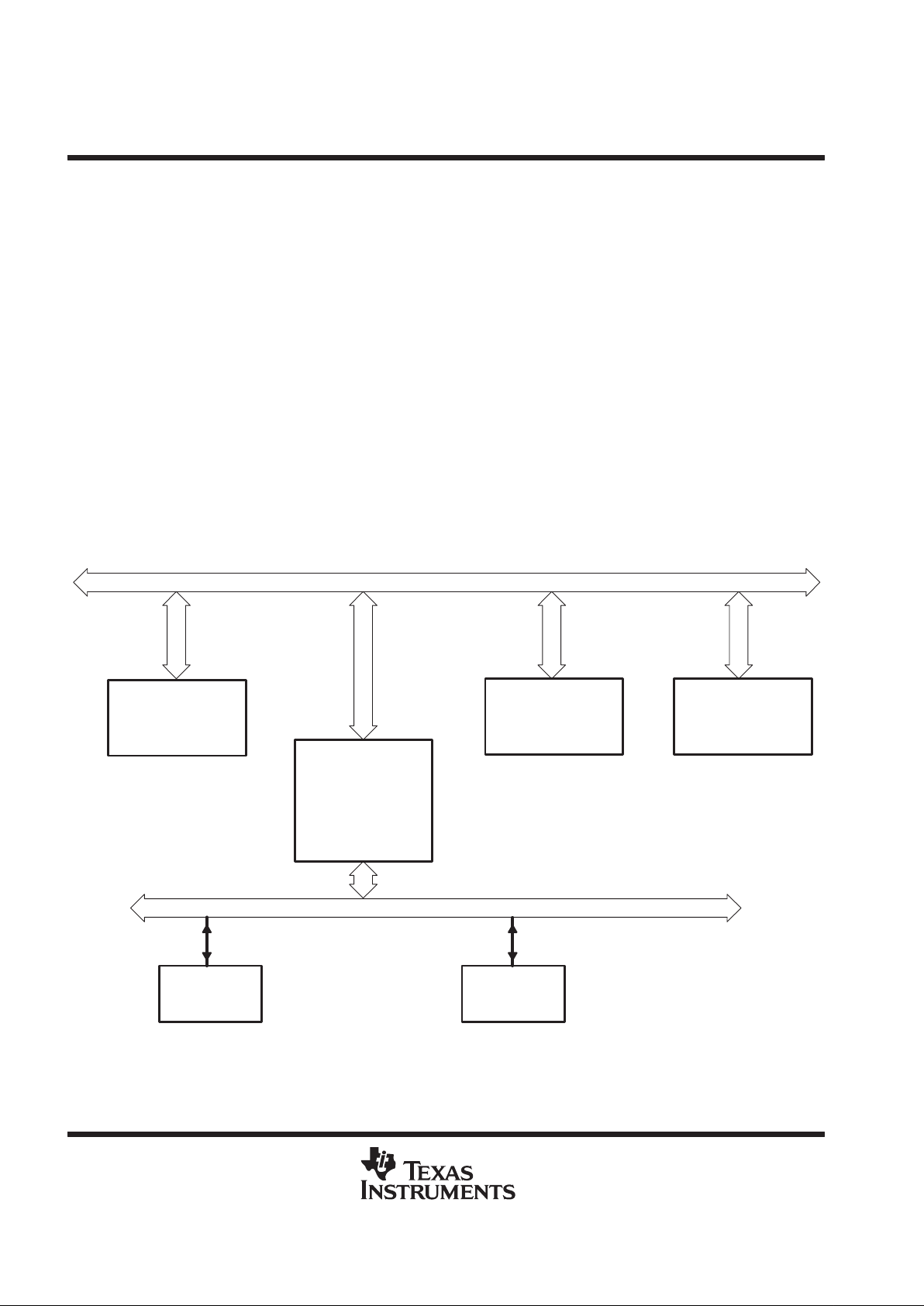
typical applications
Figure 4 shows two typical applications for the PCI2031 PCI-to-PCI bridge. A system that requires more than
ten PCI loads requires a PCI-to-PCI bridge to overcome the electrical loading limits laid out in the PCI Local Bus
Specification 2.1. Since option card slots require two loads each, bridging is necessary on large and expandable
systems. Furthermore, option cards using more than one PCI device require a PCI-to-PCI bridge to limit the load
to the option slot.
PCI Option Card
CPU
Memory
Host
Bridge
PCI2031
PCI
Device
PCI
Device
PCI Bus 0
PCI Bus 1
Host Bus
PCI Option Slot
PCI2031
PCI
Device
PCI
Device
PCI Bus 2
(Option)
PCI Option Card
Figure 4. Typical Bridge Application

PCI2031
PCI-TO-PCI BRIDGE
SCPS017A – DECEMBER 1997 – REVISED JANUARY 1998
22
POST OFFICE BOX 655303 • DALLAS, TEXAS 75265
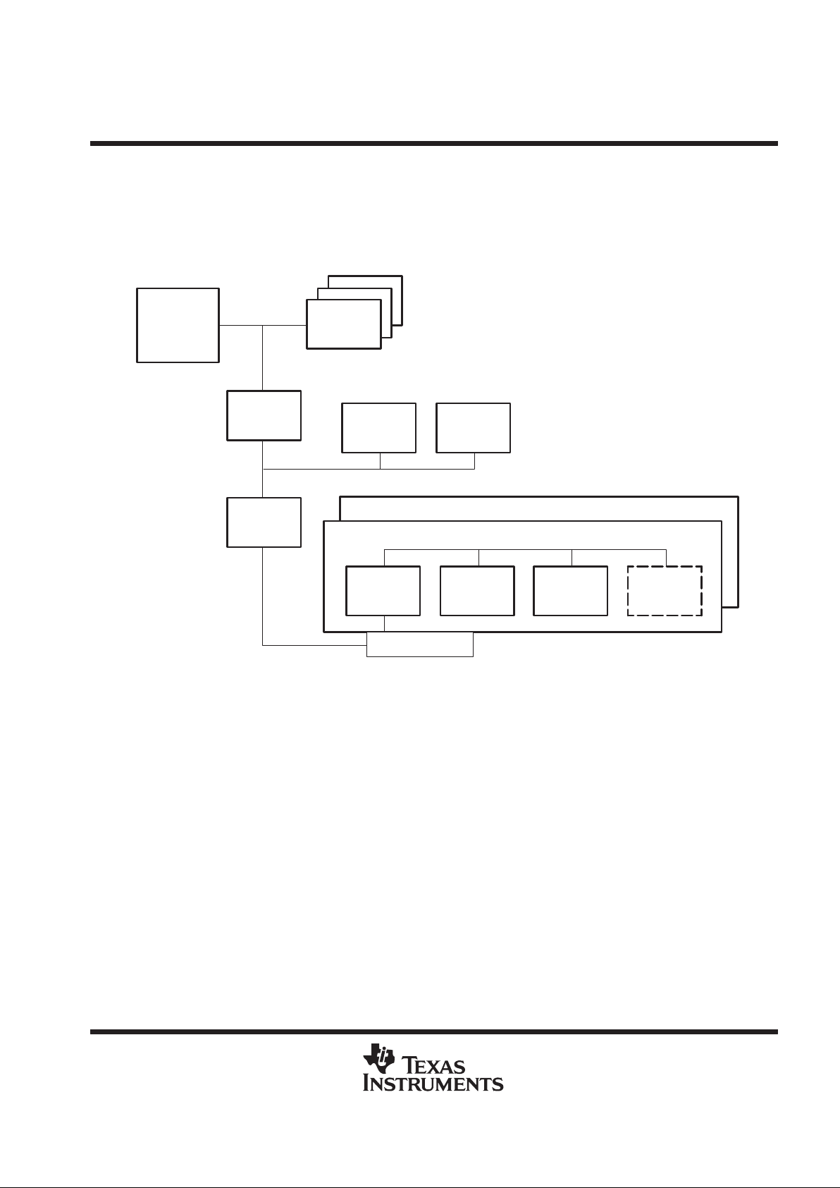
bridge configuration header
The PCI2031 bridge is a single-function PCI device. The configuration header is in compliance with the
PCI-to-PCI Bridge Architecture Specification 1.0, April 5, 1994. Table 3 shows the PCI configuration header,
which includes the predefined portion of the bridge’s configuration space. The PCI configuration offset is shown
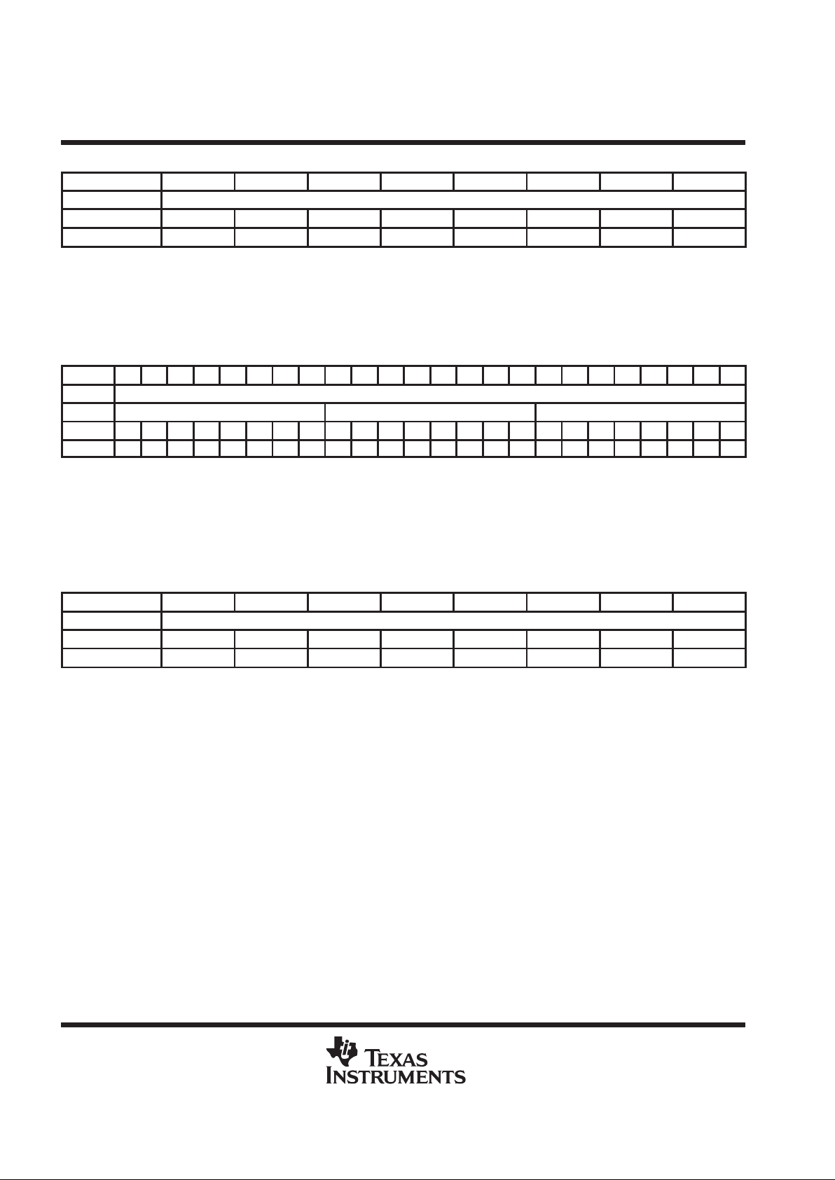
in the right column under the OFFSET heading.
Table 3. Bridge Configuration Header
REGISTER NAME OFFSET
Device ID Vendor ID 00h
Status Command 04h
Class code Revision ID 08h
BIST Header type Latency timer Cache line size 0Ch
Base address 0 10h
Base address 1 14h
Secondary bus latency timer Subordinate bus number Secondary bus number Primary bus number 18h
Secondary status I/O limit I/O base 1Ch
Memory limit Memory base 20h
Prefetchable memory limit Prefetchable memory base 24h
Prefetchable base upper 32 bits 28h
Prefetchable limit upper 32 bits 2Ch
I/O limit upper 16 bits I/O base upper 16 bits 30h
Reserved Capability pointer 34h
Expansion ROM base address 38h
Bridge control Interrupt pin Interrupt line 3Ch
Subsystem ID Subsystem vendor ID 40h
Extension window base 0 44h
Extension window limit 0 48h
Extension window base 1 4Ch
Extension window limit 1 50h
Reserved 54h–5Ch
Reserved Reserved SERR status SERR control 60h
Primary decode control Secondary decode control Extension window map Extension window enable 64h
Port decode map Port decode enable 68h
Clock run control Bridge arbitration Buffer control Secondary clock/arbiter disable 6Ch
Diagnostic status Diagnostic control 70h
GPIO output data GPIO direction control GPIO input data GPIO output select 74h
Arbiter timeout status Arbiter request mask Serialized IRQ support Docking support 78h
Reserved 7Ch
Power management capabilities Next item pointer Capability ID 80h
Reserved PMCSR Bridge Support Power management control/status 84h
Reserved 88h–EFh
Device type Device mask Chassis number Slot number F0h
Reserved F4h–FFh

PCI2031
PCI-TO-PCI BRIDGE
SCPS017A – DECEMBER 1997 – REVISED JANUARY 1998
23
POST OFFICE BOX 655303 • DALLAS, TEXAS 75265
vendor ID register
Bit 15 14 13 12 11 10 9 8 7 6 5 4 3 2 1 0
Name Vendor ID
Type R R R R R R R R R R R R R R R R
Default 0 0 0 1 0 0 0 0 0 1 0 0 1 1 0 0
Register: Vendor ID
Type: Read only
Offset: 00h
Default: 104Ch
Description: This 16-bit value is allocated by the PCI SIG (special interest group) and identifies TI as the
manufacturer of this device. The vendor ID assigned to TI is 104Ch.
device ID register
Bit 15 14 13 12 11 10 9 8 7 6 5 4 3 2 1 0
Name Device ID
Type R R R R R R R R R R R R R R R R
Default 1 0 1 0 1 1 0 0 0 0 1 0 0 0 0 1
Register: Device ID
Type: Read only
Offset: 02h
Default: AC21h
Description: This 16-bit value is allocated by the vendor and identifies the PCI device. The device ID for the
PCI2031 is AC21h.

PCI2031
PCI-TO-PCI BRIDGE
SCPS017A – DECEMBER 1997 – REVISED JANUARY 1998
24
POST OFFICE BOX 655303 • DALLAS, TEXAS 75265
command register
Bit 15 14 13 12 11 10 9 8 7 6 5 4 3 2 1 0
Name Command
Type R R R R R R R/W R/W R R/W R/W R R R/W R/W R/W
Default 0 0 0 0 0 0 0 0 0 0 0 0 0 0 0 0
Register: Command
Type: Read only, read/write (see individual bit descriptions)
Offset: 04h
Default: 0000h
Description: The command register provides control over the bridge’s interface to the primary PCI bus.
Palette snooping is enabled through this register, and all other bits adhere to the definitions in
the PCI Local Bus Specification 2.1. Table 4 describes the bit functions in the
command register.
T able 4. Command Register
BIT TYPE FUNCTION
15–10 R Reserved
9 R/W
Fast back-to-back enable. The bridge does not generate fast back-to-back transactions on the primary PCI bus. Bit 9 is
read/write, but does not affect the bridge when set. This bit defaults to 0.
8 R/W
System error (SERR) enable. Bit 8 controls the enable for the SERR driver on the primary interface.
0 = Disable SERR
driver on primary interface (default)
1 = Enable the SERR
driver on primary interface
7 R
Wait cycle control. Bit 7 controls address/data stepping by the bridge on both interfaces. The bridge does not support
address/data stepping and this bit is hardwired to 0.
6 R/W
Parity error response enable. Bit 6 controls the bridge’s response to parity errors.
0 = Parity error response disabled (default)
1 = Parity error response enabled
5 R/W
VGA palette snoop enable. When set, the bridge passes I/O writes on the primary PCI bus with addresses 3C6h, 3C8h,
and 3C9h inclusive of ISA aliases (i.e., only bits AD9–AD0 are included in the decode).
4 R Memory write and invalidate enable. In a PCI-to-PCI bridge, bit 4 must be read only and return 0 when read.
3 R
Special cycle enable. A PCI-to-PCI bridge cannot respond as a target to special cycle transactions, so bit 3 is defined as
read only and must return 0 when read.
2 R/W
Bus master enable. Bit 2 controls the bridge’s ability to initiate a cycle on the primary PCI bus. When bit 2 is 0, the bridge
does not respond to any memory or I/O transactions on the secondary interface since they cannot be forwarded to the
primary PCI bus.
0 = Bus master capability disabled (default)
1 = Bus master capability enabled
1 R/W
Memory space enable. Bit 1 controls the bridge’s response to memory accesses for both prefetchable and
nonprefetchable memory spaces on the primary PCI bus. Only when bit 1 is set will the bridge forward memory accesses
to the secondary bus from a primary bus initiator.
0 = Memory space disabled (default)
1 = Memory space enabled
0 R/W
I/O space enable. Bit 0 controls the bridge’s response to I/O accesses on the primary interface. Only when bit 0 is set will
the bridge forward I/O accesses to the secondary bus from a primary bus initiator.
0 = I/O space disabled (default)
1 = I/O space enabled

PCI2031
PCI-TO-PCI BRIDGE
SCPS017A – DECEMBER 1997 – REVISED JANUARY 1998
25
POST OFFICE BOX 655303 • DALLAS, TEXAS 75265
status register
Bit 15 14 13 12 11 10 9 8 7 6 5 4 3 2 1 0
Name Status
Type R/W R/W R/W R/W R/W R R R/W R R R R R R R R
Default 0 0 0 0 0 0 1 0 0 0 0 1 0 0 0 0
Register: Status
Type: Read only, read/write (see individual bit descriptions)
Offset: 06h
Default: 0210h
Description: The status register provides device information to the host system. This register is read only .
Bits in this register are cleared by writing a 1 to the respective bit; writing a 0 to a bit location
has no effect. Table 5 describes the status register.
Table 5. Status Register
BIT TYPE FUNCTION
15 R/W Detected parity error. Bit 15 is set when a parity error is detected.
14 R/W
Signaled system error (SERR). Bit 14 is set if SERR is enabled in the command register and the bridge signals a system
error (SERR). See
system error handling
.
0 = No SERR signaled (default)
1 = Signals SERR
13 R/W
Received master abort. Bit 13 is set when a cycle initiated by the bridge on the primary bus has been terminated by a
master abort.
0 = No master abort received (default)
1 = Master abort received
12 R/W
Received target abort. Bit 12 is set when a cycle initiated by the bridge on the primary bus has been terminated by a target
abort.
0 = No target abort received (default)
1 = Target abort received
11 R/W
Signaled target abort. Bit 1 1 is set by the bridge when it terminates a transaction on the primary bus with a target abort.
0 = No target abort signaled by the bridge (default)
1 = T arget abort signaled by the bridge
10–9 R
DEVSEL timing. These read-only bits encode the timing of P_DEVSEL and are hardwired 01b, indicating that the bridge
asserts this signal at a medium speed.
01 = Hardwired (default)
8 R/W
Data parity error detected. Bit 8 is encoded as:
0 = The conditions for setting this bit have not been met. No parity error detected. (default)
1 = A data parity error occurred and the following conditions were met:
a. P_PERR
was asserted by any PCI device including the bridge.
b. The bridge was the bus master during the data parity error.
c. The parity error response bit is set in the command register.
7 R
Fast back-to-back capable. The bridge does not support fast back-to-back transactions as a target; therefore, bit 7 is
hardwired to 0.
6 R
User-definable feature (UDF) support. The PCI2031 does not support the user-definable features; therefore, bit 6 is
hardwired to 0.
5 R 66 MHz capable. The PCI2031 operates at a maximum P_CLK frequency of 33 MHz; therefore, bit 5 is hardwired to 0.
4 R
Capabilities list. Bit 4 is read only and is hardwired to 1, indicating that capabilities additional to standard PCI are
implemented. The linked list of PCI power managment capabiities is implemented by this function.
3–0 R Reserved
PCI2031
PCI-TO-PCI BRIDGE
SCPS017A – DECEMBER 1997 – REVISED JANUARY 1998
26
POST OFFICE BOX 655303 • DALLAS, TEXAS 75265
revision ID register
Bit 7 6 5 4 3 2 1 0
Name Revision ID
Type R R R R R R R R
Default 0 0 0 0 0 0 0 0
Register: Revision ID
Type: Read only
Offset: 08h
Default: 00h (reflects the current revision of the silicon)
Description: The revision ID register indicates the silicon revision of the PCI2031.
class code register
Bit 23 22 21 20 19 18 17 16 15 14 13 12 11 10 9 8 7 6 5 4 3 2 1 0
Name Class code
Base class Sub class Programming interface
Type R R R R R R R R R R R R R R R R R R R R R R R R
Default 0 0 0 0 0 1 1 0 0 0 0 0 0 1 0 0 0 0 0 0 0 0 0 0
Register: Class code
Type: Read only
Offset: 09h
Default: 060400h
Description: The class code register categorizes the PCI2031 as a PCI-to-PCI bridge device (0604h) with a
00h programming interface (lower byte = 00h).
cache line size register
Bit 7 6 5 4 3 2 1 0
Name Cache line size
Type R/W R/W R/W R/W R/W R/W R/W R/W
Default 0 0 0 0 0 0 0 0
Register: Cache line size
Type: Read/write
Offset: 0Ch
Default: 00h
Description: The cache line size register is programmed by host software to indicate the system cache line
size needed by the bridge on memory read line and memory read multiple transactions.

PCI2031
PCI-TO-PCI BRIDGE
SCPS017A – DECEMBER 1997 – REVISED JANUARY 1998
27
POST OFFICE BOX 655303 • DALLAS, TEXAS 75265
latency timer register
Bit 7 6 5 4 3 2 1 0
Name Latency timer
Type R/W R/W R/W R/W R/W R/W R/W R/W
Default 0 0 0 0 0 0 0 0
Register: Latency timer
Type: Read/write
Offset: 0Dh
Default: 00h
Description: The latency timer register specifies the latency timer for the bridge in units of PCI clock cycles.
When the bridge is a primary PCI bus initiator and asserts P_FRAME
, the latency timer begins
counting from 0. If the latency timer expires before the bridge transaction has terminated, the
bridge terminates the transaction when its P_GNT
is deasserted.
header type register
Bit 7 6 5 4 3 2 1 0
Name Header type
Type R R R R R R R R
Default 0 0 0 0 0 0 0 1
Register: Header type
Type: Read only
Offset: 0Eh
Default: 01h
Description: The header type register is read only and returns 01h when read, indicating that the PCI2031
configuration space adheres to the PCI-to-PCI bridge configuration. Only the layout for bytes
10h–3Fh of configuration space is considered.
BIST register
Bit 7 6 5 4 3 2 1 0
Name BIST
Type R R R R R R R R
Default 0 0 0 0 0 0 0 0
Register: BIST
Type: Read only
Offset: 0Fh
Default: 00h
Description: The PCI2031 does not support built-in self test (BIST). The BIST register is read only and
returns the value 00h when read.

PCI2031
PCI-TO-PCI BRIDGE
SCPS017A – DECEMBER 1997 – REVISED JANUARY 1998
28
POST OFFICE BOX 655303 • DALLAS, TEXAS 75265
base address register 0
Bit 31 30 29 28 27 26 25 24 23 22 21 20 19 18 17 16
Name Base address register 0
Type R R R R R R R R R R R R R R R R
Default 0 0 0 0 0 0 0 0 0 0 0 0 0 0 0 0
Bit 15 14 13 12 11 10 9 8 7 6 5 4 3 2 1 0
Name Base address register 0
Type R R R R R R R R R R R R R R R R
Default 0 0 0 0 0 0 0 0 0 0 0 0 0 0 0 0
Register: Base address register 0 (BAR0)
Type: Read only
Offset: 10h
Default: 0000 0000h
Description: The bridge requires no additional resources. BAR0 is read only and returns 0s when read.
base address register 1
Bit 31 30 29 28 27 26 25 24 23 22 21 20 19 18 17 16
Name Base address register 1
Type R R R R R R R R R R R R R R R R
Default 0 0 0 0 0 0 0 0 0 0 0 0 0 0 0 0
Bit 15 14 13 12 11 10 9 8 7 6 5 4 3 2 1 0
Name Base address register 1
Type R R R R R R R R R R R R R R R R
Default 0 0 0 0 0 0 0 0 0 0 0 0 0 0 0 0
Register: Base address register 1 (BAR1)
Type: Read only
Offset: 14h
Default: 0000 0000h
Description: The bridge requires no additional resources. BAR1 is read only and returns 0s when read.
primary bus number register
Bit 7 6 5 4 3 2 1 0
Name Primary bus number
Type R/W R/W R/W R/W R/W R/W R/W R/W
Default 0 0 0 0 0 0 0 0
Register: Primary bus number
Type: Read/write
Offset: 18h
Default: 00h
Description: The primary bus number register indicates the primary bus number to which the bridge is
connected. The bridge uses this register, in conjunction with the secondary bus number and
subordinate bus number registers, to determine when to forward PCI configuration cycles to
the secondary buses.

PCI2031
PCI-TO-PCI BRIDGE
SCPS017A – DECEMBER 1997 – REVISED JANUARY 1998
29
POST OFFICE BOX 655303 • DALLAS, TEXAS 75265
secondary bus number register
Bit 7 6 5 4 3 2 1 0
Name Secondary bus number
Type R/W R/W R/W R/W R/W R/W R/W R/W
Default 0 0 0 0 0 0 0 0
Register: Secondary bus number
Type: Read/write
Offset: 19h
Default: 00h
Description: The secondary bus number register indicates the secondary bus number to which the bridge
is connected. The PCI2031 uses this register, in conjunction with the primary bus number and
subordinate bus number registers, to determine when to forward PCI configuration cycles to
the secondary buses. Configuration cycles directed to the secondary bus are converted to
type 0 configuration cycles.
subordinate bus number register
Bit 7 6 5 4 3 2 1 0
Name Subordinate bus number
Type R/W R/W R/W R/W R/W R/W R/W R/W
Default 0 0 0 0 0 0 0 0
Register: Subordinate bus number
Type: Read/write
Offset: 1Ah
Default: 00h
Description: The subordinate bus number register indicates the bus number of the highest numbered bus
beyond the primary bus existing behind the bridge. The PCI2031 uses this register, in
conjunction with the primary bus number and secondary bus number registers, to determine
when to forward PCI configuration cycles to the subordinate buses. Configuration cycles
directed to a subordinate bus (not the secondary bus) remain type 1 cycles as the cycle
crosses the bridge.
secondary bus latency timer register
Bit 7 6 5 4 3 2 1 0
Name Secondary bus latency timer
Type R/W R/W R/W R/W R/W R/W R/W R/W
Default 0 0 0 0 0 0 0 0
Register: Secondary bus latency timer
Type: Read/write
Offset: 1Bh
Default: 00h
Description: The secondary bus latency timer specifies the latency timer for the bridge in units of PCI clock
cycles. When the bridge is a secondary PCI bus initiator and asserts S_FRAME
, the latency
timer begins counting from 0. If the latency timer expires before the bridge transaction has
terminated, the bridge terminates the transaction when its S_GNT is deasserted. The
PCI-to-PCI bridge’s S_GNT is an internal signal, and is removed when another secondary bus
master arbitrates for the bus.

PCI2031
PCI-TO-PCI BRIDGE
SCPS017A – DECEMBER 1997 – REVISED JANUARY 1998
30
POST OFFICE BOX 655303 • DALLAS, TEXAS 75265
I/O base register
Bit 7 6 5 4 3 2 1 0
Name I/O base
Type R/W R/W R/W R/W R R R R
Default 0 0 0 0 0 0 0 1
Register: I/O base
Type: Read only, read/write
Offset: 1Ch
Default: 01h
Description: The I/O base register is used in decoding I/O addresses to pass through the bridge. The
bridge supports 32-bit I/O addressing; thus, bits 3–0 are read only and default to 0001b. The
upper four bits are writable and correspond to address bits AD15–AD12. The lower
12 address bits of the I/O base address are considered 0. Thus, the bottom of the defined I/O
address range is aligned on a 4K-byte boundary. The upper 16 address bits of the 32-bit I/O
base address corresponds to the contents of the I/O base upper 16-bit register (register 30h).
I/O limit register
Bit 7 6 5 4 3 2 1 0
Name I/O limit
Type R/W R/W R/W R/W R R R R
Default 0 0 0 0 0 0 0 1
Register: I/O limit
Type: Read only, read/write
Offset: 1Dh
Default: 01h
Description: The I/O limit register is used in decoding I/O addresses to pass through the bridge. The bridge
supports 32-bit I/O addressing; thus, bits 3–0 are read only and default to 0001b. The upper
four bits are writable and correspond to address bits AD15–AD12. The lower 12 address bits
of the I/O limit address are considered FFFh. Thus, the top of the defined I/O address range is
aligned on a 4K-byte boundary. The upper 16 address bits of the 32-bit I/O limit address
corresponds to the contents of the I/O limit upper 16-bit register (register 32h).

PCI2031
PCI-TO-PCI BRIDGE
SCPS017A – DECEMBER 1997 – REVISED JANUARY 1998
31
POST OFFICE BOX 655303 • DALLAS, TEXAS 75265
secondary status register
Bit 15 14 13 12 11 10 9 8 7 6 5 4 3 2 1 0
Name Secondary status
Type R/W R/W R/W R/W R/W R R R/W R R R R R R R R
Default 0 0 0 0 0 0 1 0 0 0 0 0 0 0 0 0
Register: Secondary status
Type: Read only, read/write (see individual bit descriptions)
Offset: 1Eh
Default: 0200h
Description: The secondary status register is similar in function to the status register at configuration offset
06h; however, its bits reflect status conditions of the secondary interface. Bits in this register
are cleared by writing a 1 to the respective bit.
Table 6. Secondary Status Register
BIT TYPE FUNCTION
15 R/W
Detected parity error. Bit 15 is set when a parity error is detected on the secondary interface.
0 = No parity error detected on the secondary bus (default)
1 = Parity error detected on the secondary bus
14 R/W
Received system error. Bit 14 is set when the secondary interface detects S_SERR asserted. Note that the bridge never
asserts S_SERR
.
0 = No S_SERR
detected on the secondary bus (default)
1 = S_SERR
detected on the secondary bus
13 R/W
Received master abort. Bit 13 is set when a cycle initiated by the bridge on the secondary bus has been terminated by
a master abort.
0 = No master abort received (default)
1 = Bridge master aborted the cycle
12 R/W
Received target abort. Bit 12 is set when a cycle initiated by the bridge on the secondary bus has been terminated by a
target abort.
0 = No target abort received (default)
1 = Bridge received a target abort
11 R/W
Signaled target abort. Bit 1 1 is set by the bridge when it terminates a transaction on the secondary bus with a target abort.
0 = No target abort signaled (default)
1 = Bridge signaled a target abort
10–9 R
DEVSEL timing. These read-only bits encode the timing of S_DEVSEL and are hardwired to 01b, indicating that the bridge
asserts this signal at a medium speed.
8 R/W
Data parity error detected.
0 = The conditions for setting this bit have not been met
1 = A data parity error occurred and the following conditions were met:
a. S_PERR
was asserted by any PCI device including the bridge.
b. The bridge was the bus master during the data parity error.
c. The parity error response bit is set in the bridge control register.
7 R Fast back-to-back capable. Bit 7 is hardwired to 0.
6 R User-definable feature (UDF) support. Bit 6 is hardwired to 0.
5 R 66 MHz capable. Bit 5 is hardwired to 0.
4–0 R Reserved

PCI2031
PCI-TO-PCI BRIDGE
SCPS017A – DECEMBER 1997 – REVISED JANUARY 1998
32
POST OFFICE BOX 655303 • DALLAS, TEXAS 75265
memory base register
Bit 15 14 13 12 11 10 9 8 7 6 5 4 3 2 1 0
Name Memory base
Type R/W R/W R/W R/W R/W R/W R/W R/W R/W R/W R/W R/W R R R R
Default 0 0 0 0 0 0 0 0 0 0 0 0 0 0 0 0
Register: Memory base (memory-mapped I/O base)
Type: Read only, read/write
Offset: 20h
Default: 0000h
Description: The memory base register defines the base address of a memory-mapped I/O address range
used by the bridge to determine when to forward memory transactions from one interface to
the other. The upper 12 bits of this register are read/write and correspond to the address bits
AD31–AD20. The lower 20 address bits are considered 0s; thus, the address range is aligned
to a 1M-byte boundary. The bottom four bits are read only and return 0s when read.
memory limit register
Bit 15 14 13 12 11 10 9 8 7 6 5 4 3 2 1 0
Name Memory limit
Type R/W R/W R/W R/W R/W R/W R/W R/W R/W R/W R/W R/W R R R R
Default 0 0 0 0 0 0 0 0 0 0 0 0 0 0 0 0
Register: Memory limit (memory-mapped I/O limit)
Type: Read only, read/write
Offset: 22h
Default: 0000h
Description: The memory limit register defines the upper-limit address of a memory-mapped I/O address
range used to determine when to forward memory transactions from one interface to the
other. The upper 12 bits of this register are read/write and correspond to the address bits
AD31–AD20. The lower 20 address bits are considered 1s; thus, the address range is aligned
to a 1M-byte boundary. The bottom four bits are read only and return 0s when read.
prefetchable memory base register
Bit 15 14 13 12 11 10 9 8 7 6 5 4 3 2 1 0
Name Prefetchable memory base
Type R/W R/W R/W R/W R/W R/W R/W R/W R/W R/W R/W R/W R R R R
Default 0 0 0 0 0 0 0 0 0 0 0 0 0 0 0 0
Register: Prefetchable memory base
Type: Read only, read/write
Offset: 24h
Default: 0000h
Description: The prefetchable memory base register defines the base address of a prefetchable memory
address range used by the bridge to determine when to forward memory transactions from
one interface to the other. The upper 12 bits of this register are read/write and correspond to
the address bits AD31–AD20. The lower 20 address bits are considered 0; thus, the address
range is aligned to a 1M-byte boundary. The bottom four bits are read only and return 0s
when read.

PCI2031
PCI-TO-PCI BRIDGE
SCPS017A – DECEMBER 1997 – REVISED JANUARY 1998
33
POST OFFICE BOX 655303 • DALLAS, TEXAS 75265
prefetchable memory limit register
Bit 15 14 13 12 11 10 9 8 7 6 5 4 3 2 1 0
Name Prefetchable memory limit
Type R/W R/W R/W R/W R/W R/W R/W R/W R/W R/W R/W R/W R R R R
Default 0 0 0 0 0 0 0 0 0 0 0 0 0 0 0 0
Register: Prefetchable memory limit
Type: Read only, read/write
Offset: 26h
Default: 0000h
Description: The prefetchable memory limit register defines the upper-limit address of a prefetchable
memory address range used to determine when to forward memory transactions from one
interface to the other. The upper 12 bits of this register are read/write and correspond to the
address bits AD31–AD20. The lower 20 address bits are considered 1s; thus, the address
range is aligned to a 1M-byte boundary. The bottom four bits are read only and return 0s
when read.
prefetchable base upper 32-bits register
Bit 31 30 29 28 27 26 25 24 23 22 21 20 19 18 17 16
Name Prefetchable base upper 32 bits
Type R R R R R R R R R R R R R R R R
Default 0 0 0 0 0 0 0 0 0 0 0 0 0 0 0 0
Bit 15 14 13 12 11 10 9 8 7 6 5 4 3 2 1 0
Name Prefetchable base upper 32 bits
Type R R R R R R R R R R R R R R R R
Default 0 0 0 0 0 0 0 0 0 0 0 0 0 0 0 0
Register: Prefetchable base upper 32 bits
Type: Read only
Offset: 28h
Default: 0000 0000h
Description: The PCI2031 does not support 64-bit addressing; thus, the prefetchable base upper 32-bit
register is read only and returns 0s when read.
prefetchable limit upper 32-bits register
Bit 31 30 29 28 27 26 25 24 23 22 21 20 19 18 17 16
Name Prefetchable limit upper 32 bits
Type R R R R R R R R R R R R R R R R
Default 0 0 0 0 0 0 0 0 0 0 0 0 0 0 0 0
Bit 15 14 13 12 11 10 9 8 7 6 5 4 3 2 1 0
Name Prefetchable limit upper 32 bits
Type R R R R R R R R R R R R R R R R
Default 0 0 0 0 0 0 0 0 0 0 0 0 0 0 0 0
Register: Prefetchable limit upper 32 bits
Type: Read only
Offset: 2Ch
Default: 0000 0000h
Description: The PCI2031 does not support 64-bit addressing; thus the prefetchable limit upper 32-bit
register is read only and returns 0s when read.

PCI2031
PCI-TO-PCI BRIDGE
SCPS017A – DECEMBER 1997 – REVISED JANUARY 1998
34
POST OFFICE BOX 655303 • DALLAS, TEXAS 75265
I/O base upper 16-bits register
Bit 15 14 13 12 11 10 9 8 7 6 5 4 3 2 1 0
Name I/O base upper 16 bits
Type R/W R/W R/W R/W R/W R/W R/W R/W R/W R/W R/W R/W R/W R/W R/W R/W
Default 0 0 0 0 0 0 0 0 0 0 0 0 0 0 0 0
Register: I/O base upper 16 bits
Type: Read only
Offset: 30h
Default: 0000h
Description: The I/O base upper 16-bits register specifies the upper 16 bits corresponding to AD31–AD16
of the 32-bit address that specifies the base of the I/O range to forward from the primary PCI
bus to the secondary PCI bus.
I/O limit upper 16-bits register
Bit 15 14 13 12 11 10 9 8 7 6 5 4 3 2 1 0
Name I/O limit upper 16 bits
Type R/W R/W R/W R/W R/W R/W R/W R/W R/W R/W R/W R/W R/W R/W R/W R/W
Default 0 0 0 0 0 0 0 0 0 0 0 0 0 0 0 0
Register: I/O limit upper 16 bits
Type: Read only
Offset: 32h
Default: 0000h
Description: The I/O limit upper 16-bits register specifies the upper 16 bits corresponding to AD31–AD16 of
the 32-bit address that specifies the upper limit of the I/O range to forward from the primary
PCI bus to the secondary PCI bus.
capability pointer register
Bit 7 6 5 4 3 2 1 0
Name Capability pointer register
Type R R R R R R R R
Default 1 0 0 0 0 0 0 0
Register: capability pointer
Type: Read only
Offset: 34h
Default: 80h
Description: The capability pointer register provides the pointer to the PCI configuration header where the
PCI power management register block resides. The capability pointer provides access to the
first item in the linked list of capabilities. The capability pointer register is read only and returns
80h when read, indicating the power management registers are located at PCI header offset
80h.

PCI2031
PCI-TO-PCI BRIDGE
SCPS017A – DECEMBER 1997 – REVISED JANUARY 1998
35
POST OFFICE BOX 655303 • DALLAS, TEXAS 75265
expansion ROM base address register
Bit 31 30 29 28 27 26 25 24 23 22 21 20 19 18 17 16
Name Expansion ROM base address
Type R R R R R R R R R R R R R R R R
Default 0 0 0 0 0 0 0 0 0 0 0 0 0 0 0 0
Bit 15 14 13 12 11 10 9 8 7 6 5 4 3 2 1 0
Name Expansion ROM base address
Type R R R R R R R R R R R R R R R R
Default 0 0 0 0 0 0 0 0 0 0 0 0 0 0 0 0
Register: Expansion ROM base address
Type: Read only
Offset: 38h
Default: 0000 0000h
Description: The PCI2031 does not implement the expansion ROM remapping feature. The expansion
ROM base address register returns all 0s when read.
interrupt line register
Bit 7 6 5 4 3 2 1 0
Name Interrupt line
Type R/W R/W R/W R/W R/W R/W R/W R/W
Default 1 1 1 1 1 1 1 1
Register: Interrupt line
Type: Read/write
Offset: 3Ch
Default: FFh
Description: The interrupt line register is read/write and is used to communicate interrupt line routing
information. Since the bridge does not implement an interrupt signal pin, this register defaults
to FFh.
interrupt pin register
Bit 7 6 5 4 3 2 1 0
Name Interrupt pin
Type R R R R R R R R
Default 0 0 0 0 0 0 0 0
Register: Interrupt pin
Type: Read only
Offset: 3Dh
Default: 00h
Description: The bridge default state does not implement any interrupt pins. Reads from bits 7–1 of this
register return 0s. When docking support is enabled, bit 0 of this register is 1 and bits 7–1 are 0.
NOTE:
When docking support is enabled, bit 0 is 1. P_GPIO0 should be routed to INT A
on the system board
for docking interrupt support.

PCI2031
PCI-TO-PCI BRIDGE
SCPS017A – DECEMBER 1997 – REVISED JANUARY 1998
36
POST OFFICE BOX 655303 • DALLAS, TEXAS 75265
bridge control register
Bit 15 14 13 12 11 10 9 8 7 6 5 4 3 2 1 0
Name Bridge control
Type R R R R R R R R R R/W R/W R R/W R/W R/W R/W
Default 0 0 0 0 0 0 1 1 0 1 0 0 0 0 0 0
Register: Bridge control
Type: Read only, read/write (see individual bit descriptions)
Offset: 3Eh
Default: 0000h
Description: The bridge control register provides many of the same controls for the secondary interface
that are provided by the command register for the primary interface. Some bits affect the
operation of both interfaces.

PCI2031
PCI-TO-PCI BRIDGE
SCPS017A – DECEMBER 1997 – REVISED JANUARY 1998
37
POST OFFICE BOX 655303 • DALLAS, TEXAS 75265
Table 7. Bridge Control Register
BIT TYPE FUNCTION
15–8 R Reserved. These bits are read only and return 0s when read.
7 R Fast back-to-back capable. The bridge never generates fast back-to-back transactions to different secondary devices.
6 R/W
Secondary bus reset. When bit 6 is set, the secondary reset signal (S_RST) is asserted. S_RST is deasserted by resetting
this bit. Bit 6 is encoded as:
0 = Do not force the assertion of S_RST
(default).
1 = Force the assertion of S_RST
.
5 R/W
Master abort mode. Bit 5 controls how the bridge responds to a master abort that occurs on either interface when the bridge
is the master. If this bit is set and the posted write transaction has completed on the requesting interface, if enabled
P_SERR
is asserted when a master abort occurs. If the transaction has not completed, a target abort is signaled. If the
bit is cleared, all 1s are returned on reads, and write data is accepted and discarded when a transaction that crosses the
bridge is terminated with master abort. The default state of bit 5 after a reset is 0.
0 = Do not report master aborts (return FFFF FFFFh on reads and discard data on writes) (default).
1 = Report master aborts by signaling target abort if possible, or if SERR
is enabled via bit 1 of this register,
by asserting SERR
.
4 R Reserved. Returns 0 when read. Writes have no effect.
3 R/W
VGA enable. When bit 3 is set, the bridge positively decodes and forwards VGA-compatible memory addresses in the
video frame buffer range 000A0000h–000BFFFFh, I/O addresses in the range 03B0h–03BBh, and 03C0–03DFh from
the primary to the secondary interface, independent of the I/O and memory address ranges. When this bit is set, the bridge
blocks forwarding of these addresses from the secondary to the primary. Reset clears this bit. Bit 3 is encoded as:
0 = Do not forward VGA-compatible memory and I/O addresses from the primary to the secondary interface.
(default).
1 = Forward VGA-compatible memory and I/O addresses from the primary to the secondary, independent
of the I/O and memory address ranges and independent of the ISA enable bit.
2 R/W
ISA enable. When bit 2 is set, the bridge blocks the forwarding of ISA I/O transactions from the primary to the secondary,
addressing the last 768 bytes in each 1K-byte block. This applies only to the addresses (defined by the I/O window
registers) that are located in the first 64K bytes of PCI I/O address space. From the secondary to the primary, I/O
transactions are forwarded if they address the last 768 bytes in each 1K-byte block in the address range specified in the
I/O window registers. Bit 2 is encoded as:
0 = Forward all I/O addresses in the address range defined by the I/O base and I/O limit registers (default).
1 = Block forwarding of ISA I/O addresses in the address range defined by the I/O base and I/O limit
registers when these I/O addresses are in the first 64K bytes of PCI I/O address space and address
the top 768 bytes of each 1K-byte block.
1 R/W
SERR enable. Bit 1 controls the forwarding of secondary interface SERR assertions to the primary interface. Only when
this bit is set will the bridge forward S_SERR
to the primary bus signal P_SERR. For the primary interface to assert SERR,
bit 8 of the command register must be set.
0 = SERR
disabled (default)
1 = SERR
enabled
0 R/W
Parity error response enable. Bit 0 controls the bridge’s response to parity errors on the secondary interface. When this
bit is set, the bridge asserts S_PERR
to report parity errors on the secondary interface.
0 = Ignore address and parity errors on the secondary interface (default).
1 = Enable parity error reporting and detection on the secondary interface.

PCI2031
PCI-TO-PCI BRIDGE
SCPS017A – DECEMBER 1997 – REVISED JANUARY 1998
38
POST OFFICE BOX 655303 • DALLAS, TEXAS 75265
extension registers
The TI extension registers are those registers that lie outside the standard PCI-to-PCI bridge device
configuration space (i.e., registers 40h–FFh in PCI configuration space in the PCI2031). These registers can
be accessed through configuration reads and writes. The TI extension registers add flexibility and performance
benefits to the standard PCI-to-PCI bridge.
subsystem vendor ID register
Bit 15 14 13 12 11 10 9 8 7 6 5 4 3 2 1 0
Name Subsystem vendor
Type R/W R/W R/W R/W R/W R/W R/W R/W R/W R/W R/W R/W R/W R/W R/W R/W
Default 0 0 0 0 0 0 0 0 0 0 0 0 0 0 0 0
Register: Subsystem vendor ID
Type: Read/write
Offset: 40–41h
Default: 0000h
Description: The subsystem vendor ID register is read/write and has a default value of 0000h. An add-in
card manufacturer using the PCI2031 may write to this register via a device driver for
identification purposes. Optionally, this register can also be loaded from EEPROM by the
serial EEPROM interface. In this case, device drivers should not overwrite this value.
subsystem ID register
Bit 15 14 13 12 11 10 9 8 7 6 5 4 3 2 1 0
Name Subsystem ID
Type R/W R/W R/W R/W R/W R/W R/W R/W R/W R/W R/W R/W R/W R/W R/W R/W
Default 0 0 0 0 0 0 0 0 0 0 0 0 0 0 0 0
Register: Subsystem ID
Type: Read only
Offset: 42h–43h
Default: 0000h
Description: The subsystem ID register is read/write and has a default value of 0000h. An add-in card
manufacturer using the PCI2031 may write to this register via a device driver for identification
purposes. Optionally, this register can also be loaded from EEPROM by the serial EEPROM
interface. In this case, device drivers should not overwrite this value.

PCI2031
PCI-TO-PCI BRIDGE
SCPS017A – DECEMBER 1997 – REVISED JANUARY 1998
39
POST OFFICE BOX 655303 • DALLAS, TEXAS 75265
extension window base registers 0,1
Bit 31 30 29 28 27 26 25 24 23 22 21 20 19 18 17 16
Name Extension window base 0,1
Type R/W R/W R/W R/W R/W R/W R/W R/W R/W R/W R/W R/W R/W R/W R/W R/W
Default 0 0 0 0 0 0 0 0 0 0 0 0 0 0 0 0
Bit 15 14 13 12 11 10 9 8 7 6 5 4 3 2 1 0
Name Extension window base 0,1
Type R/W R/W R/W R/W R/W R/W R/W R/W R/W R/W R/W R/W R/W R/W R R
Default 0 0 0 0 0 0 0 0 0 0 0 0 0 0 0 0
Register: Extension window base 0, 1
Type: Read only, read/write
Offset: 44h, 4Ch
Default: 0000 0000h
Description: The bridge supports two extension windows that define an address range decoded as
described in the window enable register and window map register. The extension window
base registers define the 32-bit base address of the window.
extension window limit registers 0,1
Bit 31 30 29 28 27 26 25 24 23 22 21 20 19 18 17 16
Name Extension window limit 0,1
Type R/W R/W R/W R/W R/W R/W R/W R/W R/W R/W R/W R/W R/W R/W R/W R/W
Default 0 0 0 0 0 0 0 0 0 0 0 0 0 0 0 0
Bit 15 14 13 12 11 10 9 8 7 6 5 4 3 2 1 0
Name Extension window limit 0,1
Type R/W R/W R/W R/W R/W R/W R/W R/W R/W R/W R/W R/W R/W R/W R/W R/W
Default 0 0 0 0 0 0 0 0 0 0 0 0 0 0 0 0
Register: Extension window limit 0, 1
Type: Read/write
Offset: 48h, 50h
Default: 0000 0000h
Description: The bridge supports two extension windows. Each window defines an address range that is
decoded as described in the window enable register and window map register. The extension
window limit registers define the 32-bit limit address of the window.
Bits 0 and 1 of this register determine whether the extension window is a prefetchable memory
window, a nonprefetchable window, or an I/O window. These bits are encoded as:
00 = Nonprefetchable memory
01 = Prefetchable memory
1x = I/O
Memory windows have a 4K-byte granularity and I/O windows have a double-word (4 byte)
granularity. When a memory window is selected, bits 11–2 have no effect and are assumed to
be 1s for the limit register and 0s for the base register. This is consistent with the 4K-byte
granularity of the memory windows.

PCI2031
PCI-TO-PCI BRIDGE
SCPS017A – DECEMBER 1997 – REVISED JANUARY 1998
40
POST OFFICE BOX 655303 • DALLAS, TEXAS 75265
SERR control register
Bit 7 6 5 4 3 2 1 0
Name SERR control
Type R R R/W R/W R/W R/W R/W R/W
Default 0 0 0 1 1 1 1 0
Register: SERR control
Type: Read only, read/write (see individual bit descriptions)
Offset: 60h
Default: 0Eh
Description: The system error (SERR) control register enables SERR reporting. The SERR status register
(configuration offset 61h) reflects the status of each bit in the SERR control register.
T able 8. SERR Control Register
BIT TYPE FUNCTION
7–6 R Reserved
5 R/W
Data parity error. When set, bit 5 enables PERR reporting on transactions involving data parity errors when the bridge
is mastering the bus. This bit should be enabled only when the bridge is configured for fixing parity errors.
0 = Data parity error when bridge is mastering disabled (default)
1 = Data parity error when bridge is mastering enabled
4 R/W
Discard timeout on nonprefetchable reads. When set, bit 4 enables SERR reporting when the discard timer expires on
nonprefetchable reads.
0 = Discard timeout disabled
1 = Discard timeout enabled (default)
3 R/W
Master abort on posted write transactions. When set, bit 3 enables SERR reporting on master aborts on posted write
transactions.
0 = Master aborts on posted writes disabled
1 = Master aborts on posted writes enabled (default)
2 R/W
Target abort on posted writes. When set, bit 2 enables SERR reporting on target aborts on posted write transactions.
0 = T arget aborts on posted writes disabled
1 = T arget aborts on posted writes enabled (default)
1 R/W
Parity error on posted writes. When set, bit 1 enables SERR reporting when a parity error occurs during a posted write
transaction.
0 = Parity error on posted writes
1 = Parity error on posted writes (default)
0 R/W
Arbiter timeout. When set, bit 0 enables SERR reporting when the arbiter timer expires (times out).
0 = SERR on arbiter timeout disabled (default)
1 = SERR on arbiter timeout enabled

PCI2031
PCI-TO-PCI BRIDGE
SCPS017A – DECEMBER 1997 – REVISED JANUARY 1998
41
POST OFFICE BOX 655303 • DALLAS, TEXAS 75265
SERR status register
Bit 7 6 5 4 3 2 1 0
Name SERR status
Type R R R R R R R R
Default 0 0 0 0 0 0 0 0
Register: SERR status
Type: Read only (see individual bit descriptions)
Offset: 61h
Default: 00h
Description: The SERR status register reflects the status of the SERR control register.
T able 9. SERR Status Register
BIT TYPE FUNCTION
7 R
Master timeout SERR status. When set, bit 7 indicates that SERR has occurred due to a master timeout. The master retry
enable bit (bit 15 of the diagnostic register) also enables the SERR response. Writing a 1 to this bit clears it.
0 = No SERR (default)
1 = Master timeout has caused SERR
6 R
Address parity error SERR status. When set, bit 6 indicates that SERR has occurred due to an address parity error. Writing
a 1 to this bit clears it.
0 = No SERR (default)
1 = Address parity error has caused SERR
5 R
Data parity error SERR status. When set, bit 5 indicates that SERR has occurred on a transaction involving data parity
errors while the bridge was mastering the bus. Writing a 1 to this bit clears it.
0 = No SERR (default)
1 = Data parity error while bridge was mastering has caused SERR
4 R
Discard timeout on nonprefetchable reads SERR status. When set, bit 4 indicates that SERR has occurred due to
expiration of the discard timer on nonprefetchable reads. Writing a 1 to this bit clears it.
0 = No SERR (default)
1 = Discard timeout enabled has caused an SERR
3 R
Master abort on posted write transactions SERR status. When set, bit 3 indicates that SERR has occurred due to a master
abort on a posted write transaction. Writing a 1 to this bit clears it.
0 = No SERR (default)
1 = SERR occurred due to a master abort on a posted write transaction
2 R
Target abort on posted writes SERR status. When set, bit 2 indicates that SERR has occurred due to a target abort on
a posted write transaction. Writing a 1 to this bit clears it.
0 = No SERR (default)
1 = SERR occurred due to a target abort on a posted write transaction
1 R
Parity error on posted writes SERR status. When set, bit 1 indicates that SERR has occurred due to a parity error during
a posted write transaction. Writing a 1 to this bit clears it.
0 = No SERR (default)
1 = SERR occurred due to a parity error during a posted write transaction
0 R
Arbiter timeout SERR status. When set, bit 0 indicates that SERR has occurred due to the expiration of the arbiter timer.
Writing a 1 to this bit clears it.
0 = No SERR (default)
1 = SERR occurred due to an arbiter timeout

PCI2031
PCI-TO-PCI BRIDGE
SCPS017A – DECEMBER 1997 – REVISED JANUARY 1998
42
POST OFFICE BOX 655303 • DALLAS, TEXAS 75265
extension window enable register
Bit 7 6 5 4 3 2 1 0
Name Extension window enable
Type R R R R R R R/W R/W
Default 0 0 0 0 0 0 0 0
Register: Extension window enable
Type: Read only, read/write (see individual bit descriptions)
Offset: 64h
Default: 00h
Description: The decode of the extension windows is enabled through bits 0 and 1 of this register.
Table 10. Extension Window Enable Register
BIT TYPE FUNCTION
7–2 R Reserved
1 R/W
Extension window 1 interface enable
0 – Disable window 1 (default)
1 – Enable window 1
0 R/W
Extension window 0 interface enable
0 – Disable window 0 (default)
1 – Enable window 0
extension window map register
Bit 7 6 5 4 3 2 1 0
Name Extension window map
Type R R R R R R R/W R/W
Default 0 0 0 0 0 0 0 0
Register: Extension window map
Type: Read only, read/write (see individual bit descriptions)
Offset: 65h
Default: 00h
Description: The inclusion or exclusion of the extension windows on the primary interface is selected
through bits 0 and 1 of this register. The bit descriptions discuss the decode in reference to the
primary interface. The secondary interface is the negative decode of the primary interface.
Regions excluded on the primary interface can be positively decoded on the secondary
interface if negative decoding is disabled on the secondary interface.
Table 11. Extension Window Map Register
BIT TYPE FUNCTION
7–2 R Reserved
1 R/W
Extension window 1 interface include/exclude
0 = Extension window 1 included in primary interface decode (default)
1 = Extension window 1 excluded in primary interface decode
0 R/W
Extension window 0 interface include/exclude
0 = Extension window 0 included in primary interface decode (default)
1 = Extension window 0 excluded in primary interface decode

PCI2031
PCI-TO-PCI BRIDGE
SCPS017A – DECEMBER 1997 – REVISED JANUARY 1998
43
POST OFFICE BOX 655303 • DALLAS, TEXAS 75265
secondary decode control register
Bit 7 6 5 4 3 2 1 0
Name Secondary decode control
Type R R R R R R/W R/W R/W
Default 0 0 0 0 0 1 1 0
Register: Secondary decode control
Type: Read only, read/write (see individual bit descriptions)
Offset: 66h
Default: 06h
Description: The secondary decode control register is used to enable/disable the secondary-bus negative
decoding, and only through this register can an extension window be defined for positive
decoding or excluded from negative decoding from the secondary bus to the primary bus. The
window interface bits in the window control registers must be set for the extension window
definitions in this register to have meaning.
Table 12. Secondary Decode Control Register
BIT TYPE FUNCTION
7–3 R Reserved
2 R/W
Secondary-bus subtractive decode speed. The bridge defaults to subtractive decoding after slow decode speed (four
clocks after FRAME
is asserted). Bit 0 must be set to enable subtractive decoding. When bit 0 and this bit are set,
subtractive decoding is enabled at slow decode speed. This bit is encoded as:
0 = Selects normal subtractive decode speed.
1 = Selects subtractive decode in the slow decode time slot (default).
1 R/W
Secondary bus negative decode enable. The bridge defaults to negative decoding on the secondary PCI bus. All
transactions that do not fall into windows positively decoded from the primary to the secondary are passed through to the
primary bus. This bit is encoded as:
0 = Disable secondary-bus negative decoding.
1 = Enable secondary-bus negative decoding (default).
0 R/W
Secondary-bus subtractive decode enable. The bridge defaults to negative decoding on the secondary PCI bus. When
bit 0 is set, the bridge uses subtractive decoding on the secondary bus. When the bridge is using negative decoding on
the secondary, all transactions not claimed by a slow device on the secondary bus are passed through the bridge to the
primary bus. This bit is encoded as:
0 = Disable secondary bus subtractive decoding (default).
1 = Enable secondary bus subtractive decoding.
primary decode control register
Bit 7 6 5 4 3 2 1 0
Name Primary decode control
Type R R R R R R R/W R/W
Default 0 0 0 0 0 0 0 0
Register: Primary decode control
Type: Read only, read/write (see individual bit descriptions)
Offset: 67h
Default: 00h
Description: The primary decode control register is used to enable and disable the primary-bus subtractive
decoding and to select the primary-bus subtractive decode speed. The bridge defaults to
primary-bus subtractive decoding disabled (bit 0 is cleared).

PCI2031
PCI-TO-PCI BRIDGE
SCPS017A – DECEMBER 1997 – REVISED JANUARY 1998
44
POST OFFICE BOX 655303 • DALLAS, TEXAS 75265
T able 13. Primary Decode Control Register
BIT TYPE FUNCTION
7–2 R Reserved
1 R/W
Primary-bus subtractive decode speed. The bridge defaults to subtractive decoding after slow decode speed (four clocks
after FRAME
is asserted). Bit 0 must be set to enable subtractive decoding. When bit 0 and this bit are set, subtractive
decoding is enabled at slow decode speed. This bit is encoded as:
0 = Selects normal subtractive decode speed on primary bus (default).
1 = Selects subtractive decode in the slow decode time slot on the primary bus.
0 R/W
Primary-bus subtractive decode enable. The bridge defaults to subtractive decoding disabled from the primary to
secondary PCI bus. Each PCI bus can have only one subtractive decode device.
0 = Disable primary bus subtractive decoding (default)
1 = Enable primary bus subtractive decoding
port decode enable register
Bit 15 14 13 12 11 10 9 8 7 6 5 4 3 2 1 0
Name Port decode enable
Type R R R R R R R R R R/W R/W R/W R/W R/W R/W R/W
Default 0 0 0 0 0 0 0 0 0 0 0 0 0 0 0 0
Register: Port decode enable
Type: Read only, read/write (see individual bit descriptions)
Offset: 68h–69h
Default: 0000h
Description: The port decode enable register is used to select which serial and parallel port addresses are
positively decoded from the bridge’s primary bus to the secondary bus.
Table 14. Port Decode Enable Register
BIT TYPE FUNCTION
15–7 R Reserved.
6 R/W
LPT3 enable. When bit 6 is set, the address ranges 278h–27Fh and 678h–67Bh are positively decoded and the cycles
passed to the secondary bus based on the setting of bit 6 of the port decode map register.
5 R/W
LPT2 enable. When bit 5 is set, the address ranges 378h–37Fh and 778h–77Bh are positively decoded and the cycles
passed to the secondary bus based on the setting of bit 5 of the port decode map register.
4 R/W
LPT1 enable. When bit 4 is set, the address ranges 3BCh–3BFh and 7BCh–7BFh are positively decoded and the cycles
passed to the secondary bus based on the setting of bit 4 of the port decode map register.
3 R/W
COM4 enable. When bit 3 is set, the address range 2E8h–2EFh is positively decoded and the cycles passed to the
secondary bus based on the setting of bit 3 of the port decode map register.
2 R/W
COM3 enable. When bit 2 is set, the address range 3E8h–3EFh is positively decoded and the cycles passed to the
secondary bus based on the setting of bit 2 of the port decode map register.
1 R/W
COM2 enable. When bit 1 is set, the address range 2F8h–2FFh is positively decoded and the cycles passed to the
secondary bus based on the setting of bit 1 of the port decode map register.
0 R/W
COM1 enable. When bit 0 is set, the address range 3F8h–3FFh is positively decoded and the cycles passed to the
secondary bus based on the setting of bit 0 of the port decode map register.

PCI2031
PCI-TO-PCI BRIDGE
SCPS017A – DECEMBER 1997 – REVISED JANUARY 1998
45
POST OFFICE BOX 655303 • DALLAS, TEXAS 75265
port decode map register
Bit 15 14 13 12 11 10 9 8 7 6 5 4 3 2 1 0
Name Port decode map
Type R R R R R R R R R R/W R/W R/W R/W R/W R/W R/W
Default 0 0 0 0 0 0 0 0 0 0 0 0 0 0 0 0
Register: Port decode map
Type: Read only, read/write (see individual bit descriptions)
Offset: 6Ah–6Bh
Default: 0000h
Description: The port decode map register is used to select whether the serial- and parallel-port address
ranges positively decoded from the primary bridge interface to the secondary interface are
included or excluded from the primary interface. For example, if bit 0 is set, addresses in the
range of 3F8h–3FFh are positively decoded on the primary bus. If bit 0 is cleared and an I/O
window is enabled that covers the range from 3F8h–3FFh, these addresses are claimed by
the bridge.
Table 15. Port Decode Map Register
BIT TYPE FUNCTION
15–7 R Reserved
6 R/W
LPT3 include/exclude. Bit 6 is encoded as:
0 = 278h–27Fh and 678h–67Bh excluded from the primary bus (default)
1 = 278h–27Fh and 678h–67Bh positively decoded on the primary bus
5 R/W
LPT2 include/exclude. Bit 5 is encoded as:
0 = 378h–37Fh and 778h–77Bh excluded from the primary bus (default)
1 = 378h–37Fh and 778h–77Bh positively decoded on the primary bus
4 R/W
LPT1 include/exclude. Bit 4 is encoded as:
0 = 3BCh–3BFh and 7BCh–7BFh excluded from the primary bus (default)
1 = 3BCh–3BFh and 7BCh–7BFh positively decoded on the primary bus
3 R/W
COM4 include/exclude. Bit 3 is encoded as:
0 = 2E8h–2EFh excluded from the primary bus (default)
1 = 2E8h–2EFh positively decoded on the primary bus
2 R/W
COM3 include/exclude. Bit 2 is encoded as:
0 = 3E8h–3EFh excluded from the primary bus (default)
1 = 3E8h–3EFh positively decoded on the primary bus
1 R/W
COM2 include/exclude. Bit 1 is encoded as:
0 = 2F8h–2FFh excluded from the primary bus (default)
1 = 2F8h–2FFh positively decoded on the primary bus
0 R/W
COM1 include/exclude. Bit 0 is encoded as:
0 = 3F8h–3FFh excluded from the primary bus (default)
1 = 3F8h–3FFh positively decoded on the primary bus

PCI2031
PCI-TO-PCI BRIDGE
SCPS017A – DECEMBER 1997 – REVISED JANUARY 1998
46
POST OFFICE BOX 655303 • DALLAS, TEXAS 75265
secondary clock/arbiter disable register
Bit 7 6 5 4 3 2 1 0
Name Secondary clock/arbiter disable
Type R/W R/W R/W R/W R/W R/W R/W R/W
Default 0 0 0 0 0 0 0 0
Register: Secondary clock/arbiter disable
Type: Read/write (see individual bit descriptions)
Offset: 6Ch
Default: 00h
Description: The secondary clock/arbiter disable register is used to disable each external clock to the
secondary bus. Writing a 1 to the register bit forces the corresponding clock output low. This
register is also used to disable the bridge’s internal secondary bus arbiter.
T able 16. Secondary Clock/Arbiter Disable Register
BIT TYPE FUNCTION
7 R/W
Arbiter performance-enhancement feature. When enabled, this feature provides automatic tier operation for bus masters
that have been retried or who have pending delayed transactions. In this case, the bus master gets promoted to the highest
priority tier.
0 = Disabled (default)
1 = Enabled
6 R/W
Internal arbiter disable. Bit 6 is used to disable the bridge’s internal secondary bus arbiter. When the internal arbiter is
disabled, the S_GNT0
pin becomes the secondary bus master’s request signal. S_REQ0 becomes the secondary bus
master’s grant signal.
0 = Enable internal arbiter (default)
1 = Disable internal arbiter
5 R/W
Disable clock output 5
0 = Enable clock (default)
1 = Disable clock
4 R/W
Disable clock output 4
0 = Enable clock (default)
1 = Disable clock
3 R/W
Disable clock output 3
0 = Enable clock (default)
1 = Disable clock
2 R/W
Disable clock output 2
0 = Enable clock (default)
1 = Disable clock
1 R/W
Disable clock output 1
0 = Enable clock (default)
1 = Disable clock
0 R/W
Disable clock output 0
0 = Enable clock (default)
1 = Disable clock

PCI2031
PCI-TO-PCI BRIDGE
SCPS017A – DECEMBER 1997 – REVISED JANUARY 1998
47
POST OFFICE BOX 655303 • DALLAS, TEXAS 75265
buffer control register
Bit 7 6 5 4 3 2 1 0
Name Buffer control
Type R R R/W R/W R/W R/W R/W R/W
Default 0 0 1 0 1 1 1 1
Register: Buffer control
Type: Read only, read/write (see individual bit descriptions)
Offset: 6Dh
Default: 2Fh
Description: The buffer control register allows software to enable/disable write posting and control memory
read burst prefetching. The buffer control register also enables/disables the posted memory
write reconnect feature.
Table 17. Buffer Control Register
BIT TYPE FUNCTION
7–6 R Reserved
5 R/W
Posted write reconnect enable. The bridge defaults to posted write reconnect enabled. This feature allows for a more
efficient use of the bridge FIFOs. The bridge reconnects a new posted write transaction if the following conditions are met:
1. The new posted write transaction address is 1 doubleword greater than the transaction in the FIFO.
2. There are greater than four doublewords of data in the FIFO.
3. There are greater than 4 doublewords of free space in the FIFO.
When this feature is disabled, the bridge flushes the FIFO before accepting another transaction.
0 = Disabled.
1 = Enabled. (default)
4 R/W
Upstream MRM/MRL read burst enable. By default, the PCI2031 is set to memory read burst a single cache line. By setting
this bit to 1, the PCI2031 will memory read burst multiple cache lines or until the FIFO is full. To utilize this feature, bit 3
of this register must be set to 1.
0 = Disabled. (default)
1 = Enabled.
3 R/W
Upstream memory read burst enable. The bridge defaults to upstream memory read bursting disabled. Bit 3 enables
upstream memory read bursting and indicates upstream memory is prefetchable. This bit is encoded as:
0 = Disabled (default).
1 = Enabled.
2 R/W
Downstream memory read burst enable. The bridge defaults to downstream memory read bursting enabled. Bit 2 enables
downstream memory read bursting in prefetchable windows. This bit is encoded as:
0 = Disabled.
1 = Enabled (default).
1 R/W
Secondary-to-primary write posting enable. Enables posting of write data to and from the primary interface. If bit 1 is not
set, the bridge must drain any data in its buffers before accepting data to or from the primary interface. Each data word
must then be accepted by the target before the bridge can accept the next word from the source master. The bridge must
not release the source master until the last word is accepted by the target. Operating with the write posting enabled
enhances system performance.
0 = Write posting disabled
1 = Write posting enabled (default)
0 R/W
Primary-to-secondary write posting enable. Enables posting of write data to and from the secondary interface. If bit 0 is
not set, then the bridge must drain any data in its buffers before accepting data to or from the secondary interface. Each
data word must then be accepted by the target before the bridge can accept the next word from the source master. The
bridge must not release the source master until the last word is accepted by the target. Operating with the write posting
enabled enhances system performance.
0 = Write posting disabled
1 = Write posting enabled (default)

PCI2031
PCI-TO-PCI BRIDGE
SCPS017A – DECEMBER 1997 – REVISED JANUARY 1998
48
POST OFFICE BOX 655303 • DALLAS, TEXAS 75265
bridge arbitration register
Bit 7 6 5 4 3 2 1 0
Name Bridge arbitration
Type R/W R/W R/W R/W R/W R/W R/W R/W
Default 0 1 0 0 0 0 0 0
Register: Bridge arbitration
Type: Read/write (see individual bit descriptions)
Offset: 6Eh
Default: 40h
Description: The bridge arbitration register is used for the bridge’s internal arbiter. The arbitration scheme
used is a two-tier rotational arbitration. The PCI2031 bridge is the only secondary bus initiator
that defaults to the higher priority arbitration tier. The bus-parking scheme is configured in
this register.
Table 18. Bridge Arbitration Register
BIT TYPE FUNCTION
7 R/W
Bus parking. Bit 7 determines where the PCI2031’s internal arbiter parks the secondary bus. When this bit is set, the arbiter
parks the secondary bus on the PCI2031 bridge. When this bit is cleared, the arbiter parks the secondary bus on the last
device mastering the secondary bus. This bit is encoded as:
0 = Park the secondary bus on the last secondary master (default).
1 = Park the secondary bus on the bridge.
6 R/W
Bridge tier select. Bit 6 determines in which tier the bridge is placed in the two-tier arbitration scheme. This bit is
encoded as:
0 = Lowest-priority tier
1 = Highest-priority tier (default)
5 R/W
GNT5 tier select. Bit 5 determines in which tier the S_GNT5 is placed in the arbitration scheme. This bit is encoded as:
0 = Lowest-priority tier (default)
1 = Highest-priority tier
4 R/W
GNT4 tier select. Bit 4 determines in which tier the S_GNT4 is placed in the arbitration scheme. This bit is encoded as:
0 = Lowest-priority tier (default)
1 = Highest-priority tier
3 R/W
GNT3 tier select. Bit 3 determines in which tier the S_GNT3 is placed in the arbitration scheme. This bit is encoded as:
0 = Lowest-priority tier (default)
1 = Highest-priority tier
2 R/W
GNT2 tier select. Bit 2 determines in which tier the S_GNT2 is placed in the arbitration scheme. This bit is encoded as:
0 = Lowest-priority tier (default)
1 = Highest-priority tier
1 R/W
GNT1 tier select. Bit 1 determines in which tier the S_GNT1 is placed in the arbitration scheme. This bit is encoded as:
0 = Lowest-priority tier (default)
1 = Highest-priority tier
0 R/W
GNT0 tier select. Bit 0 determines in which tier the S_GNT0 is placed in the arbitration scheme. This bit is encoded as:
0 = Lowest-priority tier (default)
1 = Highest-priority tier

PCI2031
PCI-TO-PCI BRIDGE
SCPS017A – DECEMBER 1997 – REVISED JANUARY 1998
49
POST OFFICE BOX 655303 • DALLAS, TEXAS 75265
clock run control register
Bit 7 6 5 4 3 2 1 0
Name Clock run control
Type R R R R/W R/W R/W R/W R
Default 0 0 0 0 0 0 0 0
Register: Clock run control
Type: Read only, read/write (see individual bit descriptions)
Offset: 6Fh
Default: 00h
Description: The clock run control register controls the PCI clock-run mode enable/disable. It is also used
to enable the keep-clock-running feature. Bit 0 reflects the status of the secondary clock.
There are two clock run modes supported on the secondary bus. The bridge can be
configured to stop the secondary PCI clock only in response to a request from the primary bus
to stop the clock, or it can be configured to stop the secondary clock whenever the secondary
bus is idle and there are no transaction requests from the primary bus.
There are two conditions for restarting the secondary clock. A downstream transaction
restarts the secondary clock, or if the S_CLKRUN
signal is asserted, the secondary clock
is restarted.
Table 19. Clock Run Control Register
BIT TYPE FUNCTION
7–5 R Reserved
4 R/W
Clock run mode. Bit 4 is encoded as:
0 = Stop the secondary clock only on request from the primary bus (default).
1 = Stop the secondary clock whenever the secondary bus is idle and there are no requests from the primary
bus.
3 R/W
Primary clock run enable. Bit 3 must be enabled for the bridge to respond to requests by the central resource on the primary
bus to stop the clock.
0 = Disable clock run (default)
1 = Enable clock run
2 R/W
Primary keep clock. When bit 2 is set, it causes the bridge to request that the central resource keep the PCI clock running.
. 0 = Allow primary clock to stop if secondary clock stopped (default)
1 = Always keep primary clock running
1 R/W
Secondary clock run enable
0 = Disable clock run for secondary (default)
1 = Enable clock run for secondary
0 R
Secondary clock status bit. If the clock is stopped, this bit is 1. If the clock is running, this bit is 0.
0 = Secondary clock not stopped (default)
1 = Secondary clock stopped
diagnostic control register
Bit 15 14 13 12 11 10 9 8 7 6 5 4 3 2 1 0
Name Diagnostic control
Type R/W R/W R/W R/W R/W R/W R/W R/W R/W R/W R/W R/W R/W R/W R/W R/W
Default 0 0 0 1 0 0 1 1 0 0 0 0 0 0 0 0
Register: Diagnostic control
Type: Read/write (see individual bit descriptions)
Offset: 70h–71h
Default: 1340h
Description: The diagnostic control register is used for bridge diagnostics.

PCI2031
PCI-TO-PCI BRIDGE
SCPS017A – DECEMBER 1997 – REVISED JANUARY 1998
50
POST OFFICE BOX 655303 • DALLAS, TEXAS 75265
Table 20. Diagnostic Control Register
BIT TYPE FUNCTION
15 R/W
Master retry timeout enable. When set, bit 15 enables master retry timer. This bit is encoded as:
0 = Master retry disabled (default)
1 = Master retry enabled
14 R/W
Parity mode. Bit 14 is encoded as:
0 = Parity error passing enabled (default)
1 = Parity error passing disabled
13 R/W
Upstream lock enable. The bridge default is to disable upstream lock. When set, bit 13 enables upstream resource locking.
This bit is encoded as:
0 = Selects upstream lock disabled (default)
1 = Selects upstream lock enabled
12 R/W
Downstream lock enable. The bridge default is to enable downstream lock. When set, bit 12 enables downstream resource
locking. This bit is encoded as:
0 = Selects downstream lock disabled
1 = Selects downstream lock enabled (default)
11 R/W
Secondary-bus decode speed. The bridge defaults to medium decode speed on the secondary bus. Bit 11 selects
between medium and slow decode speed. This bit is encoded as:
0 = Secondary bus decodes at medium decode speed (default)
1 = Secondary bus decodes at slow decode speed
10 R/W
Primary-bus decode speed. The bridge defaults to medium decode speed on the primary bus. Bit 10 selects between
medium and slow decode speed. This bit is encoded as:
0 = Primary bus decodes at medium decode speed (default)
1 = Primary bus decodes at slow decode speed
9 R/W
Secondary-slave discard timer enable
0 = Disable
1 = Enable (default)
8 R/W
Primary-slave discard timer enable
0 = Disable
1 = Enable (default)
7 R/W Reserved
6 R/W
Transaction ordering enable
0 = Disabled
1 = Enabled (default)
5 R/W
Secondary initial data phase counter extension
0 = Normal 16 clock to initial data phase (default)
1 = Extends initial data phase to 64 clocks
4 R/W
Primary initial data phase counter disable
0 = Enable 16 clock initial data phase counter (default)
1 = Disable 16 clock initial data phase counter
Note: The secondary initial data phase counter is always enabled.
3 R/W
Primary initial data phase counter extension
0 = Normal 16 clocks to initial data phase (default)
1 = Extends initial data phase to 64 clocks
2 R/W
Immediate retry mode
0 = Immediate retry mode enabled (default)
1 = Immediate retry mode disabled
1 R/W
Discard timer test mode. Bit 1 selects the number of clock cycles that must expire before the bridge can discard status
or data from a delayed transaction. This bit is encoded as:
0 = Discard timer 215 clocks (default)
1 = Discard timer 210 clocks
0 R/W
NAND tree test enable
0 = NAND tree test not requested (default)
1 = Request NAND tree test

PCI2031
PCI-TO-PCI BRIDGE
SCPS017A – DECEMBER 1997 – REVISED JANUARY 1998
51
POST OFFICE BOX 655303 • DALLAS, TEXAS 75265
diagnostic status register
Bit 15 14 13 12 11 10 9 8 7 6 5 4 3 2 1 0
Name Diagnostic status
Type R R R R R/W R/W R/W R/W R R R R/W R/W R R R/W
Default 0 0 0 0 0 0 0 0 0 0 0 0 0 0 0 0
Register: Diagnostic status
Type: Read only, read/write (see individual bit descriptions)
Offset: 72h–73h
Default: 0000h
Description: The diagnostic status register is used to reflect the bridge diagnostic status.
Table 21. Diagnostic Status Register
BIT TYPE FUNCTION
15–12 R Reserved
11 R/W
Bridge detected a parity error while mastering on the secondary bus. When set, bit 11 indicates that the secondary bus
master detected a parity error. W riting a 1 to this bit clears it.
0 = No parity error detected
1 = Parity error detected
10 R/W
Bridge detected a parity error while mastering on the primary bus. When set, bit 10 indicates that the primary bus master
detected a parity error. Writing a 1 to this bit clears it.
0 = No parity error detected
1 = Parity error detected
9 R/W
Secondary-slave discard timer expired. Writing a 1 to this bit clears it.
0 = Discard timer not expired
1 = Discard timer expired
8 R/W
Primary-slave discard timer expired. Writing a 1 to this bit clears it.
0 = Discard timer not expired
1 = Discard timer expired
7–5 R Reserved
4 R/W
Serial EEPROM detect status. When bit 4 is cleared, it indicates that the serial EEPROM block detected an EEPROM.
Writing a 1 to this bit clears it. This bit is encoded as:
0 = Serial EEPROM block detected an EEPROM.
1 = Serial EEPROM block did not detect an EEPROM.
3 R/W
Serial EEPROM block error status. Bit 3 indicates the error status of the serial EEPROM block. This bit is set when a data
error has occurred in the serial EEPROM block. Writing a 1 to this bit clears it. This bit is encoded as:
0 = No error detected.
1 = Data error detected.
2 R
External arbiter enable pin status. Bit 2 contains the current state of the external pin external arbiter enable.
0 = Signal low
1 = Signal high
1 R
Serial EEPROM block status. Bit 1 indicates the status of the serial EEPROM block. When set, bit 1 indicates that the
serial EEPROM block is busy.
0 = Serial EEPROM block not busy
1 = Serial EEPROM block busy
0 R/W
Arbiter timeout status. Bit 0 indicates the status of the arbiter timer. When set, bit 0 indicates that a bus master did not
begin the cycle within 16 clocks. Writing a 1 to this bit clears it. This bit is encoded as:
0 = No timeout (default).
1 = Master requesting the bus did not start cycle within 16 clocks.

PCI2031
PCI-TO-PCI BRIDGE
SCPS017A – DECEMBER 1997 – REVISED JANUARY 1998
52
POST OFFICE BOX 655303 • DALLAS, TEXAS 75265
GPIO output select register
Bit 7 6 5 4 3 2 1 0
Name GPIO output select
Type R/W R/W R/W R/W R/W R/W R/W R/W
Default 0 0 0 0 0 0 0 0
Register: GPIO output select
Type: Read/write (see individual bit descriptions)
Offset: 74h
Default: 00h
Description: The GPIO output select register is used for debug purposes. P_GPIO0 can be configured as
an output and used as an interrupt request from the PCI2031 when docking support is
enabled. P_GPIO2 and P_GPIO3 can be configured as input pins and used as docking station
support detect pins 1 and 2, respectively. S_GPIO0 and S_GPIO1 are used for the serial
EEPROM interface when implemented; S_GPIO0 serves as the clock line and S_GPIO1
serves as the data line. P_GPIO1 and S_GPIO2 can be used as the primary and secondary
bus IRQSER pins, respectively.
Table 22. GPIO Output Select Register
BIT TYPE FUNCTION
7 R/W
S_GPIO3. The value of bit 7 selects the function of S_GPIO3.
0 = Normal GPIO output data (default)
1 = Internal test signal that is asserted low when DEVSEL is driven by bridge on secondary bus
6 R/W
S_GPIO2. If serialized IRQ support is enabled via bit 0 of the serial IRQ support register, configuration offset 79h,
S_GPIO2 is used as the secondary IRQSER pin.
0 = Normal GPIO output data (default)
1 = Selects internal test signal that is asserted low when frame is driven by bridge on secondary bus
5 R/W
S_GPIO1. If an EEPROM is present in the system, S_PGIO1 is used for the serial EEPROM interface.
0 = Normal GPIO output data (default)
1 = Selects bridge grant signal to PCI secondary interface
4 R/W
S_GPIO0. If an EEPROM is present in the system, S_PGIO0 is used for the serial EEPROM interface.
0 = Normal GPIO output data (default)
1 = Selects bridge request signal from PCI secondary interface
3 R/W
P_GPIO3. If docking support is enabled via bit 0 of the docking support register, configuration of fset 78h, P_GPIO3 is used
as docking change detect pin 2.
0 = Normal GPIO output data (default)
1 = Selects internal test signal that is asserted low when DEVSEL is driven by bridge on primary bus
2 R/W
P_GPIO2. If docking support is enabled via bit 0 of the docking support register, configuration of fset 78h, P_GPIO2 is used
as docking change detect pin 1.
0 = Normal GPIO output data (default)
1 = Selects internal test signal that is asserted low when frame is driven by bridge on primary bus
1 R/W
P_GPIO1. If serialized IRQ support is enabled via bit 0 of the serial IRQ support register, configuration offset 79h,
P_GPIO1 is used as the primary IRQSER pin.
0 = Normal GPIO output data (default)
1 = Selects signal indicating the primary PCI interface is locked as a resource
0 R/W
P_GPIO0. If docking support is enabled via bit 0 of the docking support register, configuration of fset 78h, P_GPIO0 is used
as the interrupt request from the bridge.
0 = Normal GPIO output data (default)
1 = Selects internal test signal that is asserted high when 16 clock arbitration timeout occurs

PCI2031
PCI-TO-PCI BRIDGE
SCPS017A – DECEMBER 1997 – REVISED JANUARY 1998
53
POST OFFICE BOX 655303 • DALLAS, TEXAS 75265
GPIO input data register
Bit 7 6 5 4 3 2 1 0
Name GPIO input data
Type R R R R R R R R
Default X X X X X X X X
Register: GPIO input data
Type: Read only (see individual bit descriptions)
Offset: 75h
Default: XXh
Description: The GPIO input data register reflects the state of the GPIO pins.
Table 23. GPIO Input Data Register
BIT TYPE FUNCTION
7–4 R
S_GPIO3–S_GPIO0 pin state
0 = Low
1 = High
3–0 R
P_GPIO3–P_GPIO0 pin state
0 = Low
1 = High
GPIOx input data bit
Debug test data
GPIOx output data bit
GPIOx output select bit
0 = GPIOx output
1 = Other function
GPIOx direction control bit
0 = Input
1 = Output
Figure 5. GPIO Buffer

PCI2031
PCI-TO-PCI BRIDGE
SCPS017A – DECEMBER 1997 – REVISED JANUARY 1998
54
POST OFFICE BOX 655303 • DALLAS, TEXAS 75265
GPIO direction control register
Bit 7 6 5 4 3 2 1 0
Name GPIO direction control
Type R/W R/W R/W R/W R/W R/W R/W R/W
Default 0 0 0 0 0 0 0 0
Register: GPIO direction control
Type: Read/write (see individual bit descriptions)
Offset: 76h
Default: 00h
Description: The GPIO direction control register controls the direction of the GPIO pins.
Table 24. GPIO Direction Control Register
BIT TYPE FUNCTION
7–4 R/W
S_GPIO3–S_GPIO0 pin state
0 = Input (default)
1 = Output
3–0 R/W
P_GPIO3–P_GPIO0 pin state
0 = Input (default)
1 = Output
GPIO output data register
Bit 7 6 5 4 3 2 1 0
Name GPIO output data
Type R/W R/W R/W R/W R/W R/W R/W R/W
Default 0 0 0 0 0 0 0 0
Register: GPIO output data
Type: Read/write (see individual bit descriptions)
Offset: 77h
Default: 00h
Description: The GPIO output data register contains the output data for any selected GPIO pin.
Table 25. GPIO Output Data Register
BIT TYPE FUNCTION
7–4 R/W
S_GPIO3–S_GPIO0 output data
0 = Data-out value if selected is 0 (default)
1 = Data-out value if selected is 1
3–0 R/W
P_GPIO3–P_GPIO0 output data
0 = Data-out value if selected is 0 (default)
1 = Data-out value if selected is 1

PCI2031
PCI-TO-PCI BRIDGE
SCPS017A – DECEMBER 1997 – REVISED JANUARY 1998
55
POST OFFICE BOX 655303 • DALLAS, TEXAS 75265
docking support register
Bit 7 6 5 4 3 2 1 0
Name Docking support
Type R R R R R/W R/W R/W R/W
Default 0 0 0 0 0 0 0 0
Register: Docking support
Type: Read only, read/write (see individual bit descriptions)
Offset: 78h
Default: 00h
Description: The docking support register is used for docking support. A change in state on the P_GPIO3
pin or the P_GPIO2 pin is reflected as a change on the P_GPIO0 pin.
Table 26. Docking Support Register
BIT TYPE FUNCTION
7–4 R Reserved
3 R/W
P_GPIO3 change detect status. A change in bit 3 is reflected on the P_GPIO0 pin.
0 = No change (default)
1 = Change has occurred. Write a 1 to clear this bit.
2 R/W
P_GPIO2 change detect status. A change in bit 2 is reflected on the P_GPIO0 pin.
0 = No change (default)
1 = Change has occurred. Write a 1 to clear this bit.
1 R/W
Single line select
0 = Single line connect detect (default)
1 = Two line connect detect
0 R/W
Docking support enable
0 = Disable (default)
1 = Enable

PCI2031
PCI-TO-PCI BRIDGE
SCPS017A – DECEMBER 1997 – REVISED JANUARY 1998
56
POST OFFICE BOX 655303 • DALLAS, TEXAS 75265
serialized IRQ support register
Bit 7 6 5 4 3 2 1 0
Name Serialized IRQ support
Type R R/W R/W R/W R/W R/W R/W R/W
Default 0 0 0 0 0 0 0 0
Register: Serialized IRQ support
Type: Read/write (see individual bit descriptions)
Offset: 79h
Default: 00h
Description: The serialized IRQ support register is used to configure the serialized IRQ stream. Serialized
IRQ support is enabled/disabled via bit 0 of the serialized IRQ support register. The start
frame is variable from four to six PCI clocks wide. The bridge does not support an 8-clock start
frame. Bits 2 and 1 are used to configure the number of clocks in the start frame. Bits 6–3 are
used to configure the number of data frames in the serialized IRQ stream – up to 32 data
frames are permitted, including the start frame, the I/O channel check frame, and the stop
frame. The host controller must do one stream in continuous mode before switching to quiet
mode. The continuous stream must be for 17 data frames.
Table 27. Serialized IRQ Support Register
BIT TYPE FUNCTION
7 R Reserved
6–3 R/W
Number of IRQ/data frames. These bits determine the number of IRQ/data frames for the serialized IRQ stream. The host
is required to support a minimum of 17 IRQ/data frames and a maximum of 32. These bits are encoded as:
0000 = 17 IRQ/data frames (default)
0001 = 18 IRQ/data frames
0010 = 19 IRQ/data frames
0011 = 20 IRQ/data frames
0100 = 21 IRQ/data frames
0101 = 22 IRQ/data frames
0110 = 23 IRQ/data frames
0111 = 24 IRQ/data frames
1000 = 25 IRQ/data frames
1001 = 26 IRQ/data frames
1010 = 27 IRQ/data frames
1011 = 28 IRQ/data frames
1100 = 29 IRQ/data frames
1101 = 30 IRQ/data frames
1110 = 31 IRQ/data frames
1111 = 32 IRQ/data frames
2–1 R/W
Start frame clock select. These bits determine the number of PCI clock cycles in the start frame. The PCI2031 bridge does
not support an 8-clock start frame. These bits are encoded as:
00 = 4 clock cycles per start frame (default)
01 = 6 clock cycles per start frame
10 = 4 clock cycles per start frame
11 = 6 clock cycles per start frame
0 R/W
Serialized IRQ support enable. Bit 0 is used to enable/disable serialized IRQ support. It is encoded as:
0 = Serialized IRQ support disabled (default)
1 = Serialized IRQ support enabled

PCI2031
PCI-TO-PCI BRIDGE
SCPS017A – DECEMBER 1997 – REVISED JANUARY 1998
57
POST OFFICE BOX 655303 • DALLAS, TEXAS 75265
arbiter request mask register
Bit 7 6 5 4 3 2 1 0
Name Arbiter request mask
Type R R/W R/W R/W R/W R/W R/W R/W
Default 0 0 0 0 0 0 0 0
Register: Arbiter request mask
Type: Read/write (see individual bit descriptions)
Offset: 7Ah
Default: 00h
Description: The arbiter request mask register contains the SERR enable on arbiter timeouts and the
request mask controls.
Table 28. Arbiter Request Mask Register
BIT TYPE FUNCTION
7 R Reserved
6 R/W
Timeout automatic masking enable
0 = Masking not automatic (default)
1 = Allow masking after 16 clock timeouts
5 R/W
Request 5 (REQ5) mask bit
0 = Use request 5 (default)
1 = Ignore request 5
4 R/W
Request 4 (REQ4) mask bit
0 = Use request 4 (default)
1 = Ignore request 4
3 R/W
Request 3 (REQ3) mask bit
0 = Use request 3 (default)
1 = Ignore request 3
2 R/W
Request 2 (REQ2) mask bit
0 = Use request 2 (default)
1 = Ignore request 2
1 R/W
Request 1 (REQ1) mask bit
0 = Use request 1 (default)
1 = Ignore request 1
0 R/W
Request 0 (REQ0) mask bit
0 = Use request 0 (default)
1 = Ignore request 0

PCI2031
PCI-TO-PCI BRIDGE
SCPS017A – DECEMBER 1997 – REVISED JANUARY 1998
58
POST OFFICE BOX 655303 • DALLAS, TEXAS 75265
arbiter timeout status register
Bit 7 6 5 4 3 2 1 0
Name Arbiter timeout status
Type R R R R R R R R
Default 0 0 0 0 0 0 0 0
Register: Arbiter timeout status
Type: Read only (see individual bit descriptions)
Offset: 7Bh
Default: 00h
Description: The arbiter timeout status register contains the status of each request (request 5–0) timeout.
The timeout status bit for the respective request is set if the device did not assert FRAME
after
16 clocks.
Table 29. Arbiter Timeout Status Register
BIT TYPE FUNCTION
7–6 R Reserved
5 R
Request 5 timeout status. Cleared by writing a 1.
0 = No timeout (default)
1 = Timeout has occurred
4 R
Request 4 timeout status. Cleared by writing a 1.
0 = No timeout (default)
1 = Timeout has occurred
3 R
Request 3 timeout status. Cleared by writing a 1.
0 = No timeout (default)
1 = Timeout has occurred
2 R
Request 2 timeout status. Cleared by writing a 1.
0 = No timeout (default)
1 = Timeout has occurred
1 R
Request 1 timeout status. Cleared by writing a 1.
0 = No timeout (default)
1 = Timeout has occurred
0 R
Request 0 timeout status. Cleared by writing a 1.
0 = No timeout (default)
1 = Timeout has occurred
capability ID register
Bit 7 6 5 4 3 2 1 0
Name Capability ID
Type R R R R R R R R
Default 0 0 0 0 0 0 0 1
Register: Capability ID
Type: Read only
Offset: 80h
Default: 01h
Description: The cability ID register identifies the linked list item as the register for PCI Power
Management. The cability ID register returns 01h when read, which is the unique ID assigned
by the PCI SIG for PCI location of the capabilities pointer and the value.

PCI2031
PCI-TO-PCI BRIDGE
SCPS017A – DECEMBER 1997 – REVISED JANUARY 1998
59
POST OFFICE BOX 655303 • DALLAS, TEXAS 75265
next item pointer register
Bit 7 6 5 4 3 2 1 0
Name Next item pointer
Type R R R R R R R R
Default 0 0 0 0 0 0 0 0
Register: Next item pointer
Type: Read only
Offset: 81h
Default: 00h
Description: The next item pointer register is used to indicate the next item in the linked list of PCI power
management capabilities. Since the PCI2031 only provides one capabilities list item, this
register returns zeros when read.
power management capabilities register
Bit 15 14 13 12 11 10 9 8 7 6 5 4 3 2 1 0
Name Power management capabilities
Type R R R R R R R R R R R R R R R R
Default 0 0 0 0 0 1 1 0 0 0 0 0 0 0 0 1
Register: Power management capabilities
Type: Read only
Offset: 82h
Default: 0601h
Description: The power management capabilities register contains information on the capabilities of the
PCI2031 functions related to power management. The PCI2031 function supports D0, D1,
D2, and D3 power states.
Table 30. Power Management Capabilities Register
BIT TYPE FUNCTION
15–11 R
PME Support. This five bit field indicates the power states that the device supports asserting PME#. A ‘0’ for
any of these bits indicates that the PCI2031 cannot assert PME# signal from that power state. For the
PCI2031, these five bits return ‘00000b’ when read indicating that PME# is not supported.
10 R
D2 Support. This bit returns ‘1’ when read, indicating that the Bridge function supports the D2 device power
state.
9 R
D1 Support. This bit returns ‘1’ when read, indicating that the Bridge function supports the D1 device power
state.
8–6 R Reserved.
5 R
Device Specific Initialization. This bit is read only and returns ‘0’ when read, indicating that the bridge function
does not require special initialization (beyond the standard PCI configuration header) before the generic class
device driver is able to use it.
4 R
Auxilliary Power Source. This bit is read only and returns a ‘0’ because the PCI2031 does not support PME#
signaling.
3 R PMECLK. This bit is read only and returns a ‘0’ because the PME# signaling is not supported.
2–0 R
Version. This three bit register returns ‘001b’ when read, indicating Revision 1.0 of PCI Bus Power
Management Interface Specification.

PCI2031
PCI-TO-PCI BRIDGE
SCPS017A – DECEMBER 1997 – REVISED JANUARY 1998
60
POST OFFICE BOX 655303 • DALLAS, TEXAS 75265
power management control/status register
Bit 15 14 13 12 11 10 9 8 7 6 5 4 3 2 1 0
Name Power management control/status
Type R R R R R R R R R R R R R R R/W R/W
Default 0 0 0 0 0 0 0 0 0 0 0 0 0 0 0 0
Register: Power management control/status
Type: Read only, Read/Write
Offset: 84h
Default: 0000h
Description: The power management control/status register determines and changes the current power
state of the PCI2031. The contents of this register are not affected by the internally generated
reset caused by the transition from D3hot to D0 state.
Table 31. Power Management Capabilities Register
BIT TYPE FUNCTION
15 R PME Status. This bit is read only and returns a zero because the PCI2031 does not support PME#.
14–13 R
Data Scale. This two bit field is read only returning zeros when read. The PCI2031 function does not return
any dynamic data, as indicated by the DYNAMIC DATA bit.
12–9 R
Data Select. This four bit field is read only returning zeros when read. The PCI2031 function does not return
any dynamic data, as indicated by the DYNAMIC DATA bit.
8 R PME Enable. This bit is read only and returns a zero because the PCI2031 does not support PME# signaling.
7–2 R Reserved. These bits are read only and return zeros when read.
1–0 R/W
Power State. This two bit field is used both to determine the current power state of a function and to set the
function into a new power state. The definition of the two bit field is given below:
00 – D0
01 – D1
10 – D2
11 – D3hot
PMCSR bridge support
Bit 7 6 5 4 3 2 1 0
Name PMCSR bridge support
Type R R R R R R R R
Default 1 1 0 0 0 0 0 0
Register: PMCSR bridge support
Type: Read only
Offset: 86h
Default: C0h
Description: The PMCSR bridge support register is required for all PCI bridges and supports PCI bridge
specific functionality.

PCI2031
PCI-TO-PCI BRIDGE
SCPS017A – DECEMBER 1997 – REVISED JANUARY 1998
61
POST OFFICE BOX 655303 • DALLAS, TEXAS 75265
T able 32. PMCSR Bridge Support Register
BIT TYPE FUNCTION
7 R
Bus Power Control Enable. This bit is read only and returns a one when read indicating that the power
management state of the secondary bus follows that of the PCI2031 with one exception, D3hot state. The
action that occurs when the PCI2031 is programmed to D3hot state is determined by the B2/B3 Support bit.
6 R
B2/B3 Support for D3hot. This bit is read only and returns a one when read indicating that when the PCI2031
is programmed to D3hot state the secondary bus’s clock is stopped (B2).
5–0 R Reserved.
slot number register
Bit 7 6 5 4 3 2 1 0
Name Slot number
Type R/W R/W R/W R/W R/W R/W R/W R/W
Default 0 0 0 0 0 0 0 0
Register: Slot number
Type: Read/write (see individual bit descriptions)
Offset: F0h
Default: 00h
Description: The slot number register is configured by an EEPROM at system power up. While the
EEPROM is loading data into this register, the PCI2031 retries all configuration read accesses
to this register and to the subsystem vendor ID register (40h). Configuration read accesses to
register 2Ch and register 40h for devices 0–7 on the PCI2031 secondary are also retried while
the EEPROM is loading data into the PCI2031 subsystem vendor ID and slot
number registers.
Table 33. Slot Number Register
BIT TYPE FUNCTION
7–6 R/W Reserved
5 R/W
Slots follow parent. If bit 5 is 0, it indicates that this bridge is a parent bridge. In this case, the slot number is equal to the
PCI device number. If bit 5 is 1 in this bridge configuration, software must calculate the slot number . See Appendix B,
Slot
Numbering,
in the PCI-to-PCI bridge specification for details on calculating the slot number.
4–0 R/W
Expansion slots provided. This value is used to calculate the slot number for a device in an expansion chassis. See
Appendix B,
Slot Numbering,
in the PCI-to-PCI bridge specification for details on calculating the slot number.

PCI2031
PCI-TO-PCI BRIDGE
SCPS017A – DECEMBER 1997 – REVISED JANUARY 1998
62
POST OFFICE BOX 655303 • DALLAS, TEXAS 75265
chassis number register
Bit 7 6 5 4 3 2 1 0
Name Chassis number
Type R/W R/W R/W R/W R/W R/W R/W R/W
Default 0 0 0 0 0 0 0 0
Register: Chassis number
Type: Read/write
Offset: F1h
Default: 00h
Description: This 8-bit register designates the chassis number in which the slots on the bridge’s secondary
bus reside. The chassis number register is configured by the system configuration software at
system power up and each time the system is reconfigured. The main chassis is always
chassis 0. Conflicts between chassis are resolved automatically every time the system is
powered up.
device mask register
Bit 7 6 5 4 3 2 1 0
Name Device mask
Type R/W R/W R/W R/W R/W R/W R/W R/W
Default 0 0 0 0 0 0 0 0
Register: Device mask
Type: Read/write (see individual bit descriptions)
Offset: F2h
Default: 00h
Description: The device mask register is configured from an EEPROM during system boot up. The bits in
this register control access to the subsystem vendor ID register of devices on the secondary
bus of the bridge. Each bit of this register corresponds to the device on the secondary of the
same number. For example, bit 0 of this register corresponds to device zero on the secondary
bus, bit 1 corresponds to device one on the secondary bus, and so on. If the bit value is 1, it
indicates that the corresponding device is masked. If the bit is 0, it indicates that the
corresponding device is not masked.
Table 34 describes the bits in the device mask register. The PCI2031 supports up to six
devices on its secondary bus – up to eight if an external arbiter is used. The device number is
encoded in bits 13–11 of the PCI AD bus during a configuration cycle.
Table 35 describes the results of configuration read accesses to the subsystem vendor ID
register of devices on the secondary based on the bits of this register and the corresponding
bits in the device-type register. For example, if bit 3 of the device mask register is 0, and bit 3 of
the device-type register is 1 (01), then read accesses to the subsystem vendor ID registers
(2Ch for nonbridge devices and 40h for bridge devices) of device number 3 are passed
through the bridge to the device 3 on the secondary bus. The bridge does not return any data.
If bit 5 of the device mask register is 1, and bit 5 of the device-type register is 1, read accesses
to register 40h of device 5 are masked and the bridge returns data from its own register 40h. In
Table 35, n = 0, 1, 2, 3, 4, 5, 6, or 7.

PCI2031
PCI-TO-PCI BRIDGE
SCPS017A – DECEMBER 1997 – REVISED JANUARY 1998
63
POST OFFICE BOX 655303 • DALLAS, TEXAS 75265
Table 34. Device Mask Register
BIT TYPE FUNCTION
7 R/W
Bit 7 corresponds to device 7 on the secondary bus. When this bit is 1, it indicates that configuration read accesses to
register 2Ch of a nonbridge device or register 40h of a bridge device are masked.
0 = Read accesses to register 2Ch/40h are not masked (default)
1 = Read accesses to register 2Ch/40h are masked
6 R/W
Bit 6 corresponds to device 6 on the secondary bus. When this bit is 1, it indicates that configuration read accesses to
register 2Ch of a nonbridge device or register 40h of a bridge device are masked.
0 = Read accesses to register 2Ch/40h are not masked (default)
1 = Read accesses to register 2Ch/40h are masked
5 R/W
Bit 5 corresponds to device 5 on the secondary bus. When this bit is 1, it indicates that configuration read accesses to
register 2Ch of a nonbridge device or register 40h of a bridge device are masked.
0 = Read accesses to register 2Ch/40h are not masked (default)
1 = Read accesses to register 2Ch/40h are masked
4 R/W
Bit 4 corresponds to device 4 on the secondary bus. When this bit is 1, it indicates that configuration read accesses to
register 2Ch of a nonbridge device or register 40h of a bridge device are masked.
0 = Read accesses to register 2Ch/40h are not masked (default)
1 = Read accesses to register 2Ch/40h are masked
3 R/W
Bit 3 corresponds to device 3 on the secondary bus. When this bit is 1, it indicates that configuration read accesses to
register 2Ch of a nonbridge device or register 40h of a bridge device are masked.
0 = Read accesses to register 2Ch/40h are not masked (default)
1 = Read accesses to register 2Ch /40h are masked
2 R/W
Bit 2 corresponds to device 2 on the secondary bus. When this bit is 1, it indicates that configuration read accesses to
register 2Ch of a nonbridge device or register 40h of a bridge device are masked.
0 = Read accesses to register 2Ch/40h are not masked (default)
1 = Read accesses to register 2Ch/40h are masked
1 R/W
Bit 1 corresponds to device 1 on the secondary bus. When this bit is 1, it indicates that configuration read accesses to
register 2Ch of a nonbridge device or register 40h of a bridge device are masked.
0 = Read accesses to register 2Ch/40h are not masked (default)
1 = Read accesses to register 2Ch/40h are masked
0 R/W
Bit 0 corresponds to device 0 on the secondary bus. When this bit is 1, it indicates that configuration read accesses to
register 2Ch of a nonbridge device or register 40h of a bridge device are masked.
0 = Read accesses to register 2Ch/40h are not masked (default)
1 = Read accesses to register 2Ch/40h are masked
Table 35. Configuration Read Access Results
REGISTER
DEVICE MASK,
BIT n
DEVICE TYPE,
BIT n
RESULTS OF CONFIGURATION READ ACCESS
0 0
Read accesses to registers 2Ch/40h of device number n on the secondary bus are passed through
the bridge. The bridge does not return any data.
0 1
Read accesses to registers 2Ch/40h of device number n on the secondary bus are passed through
the bridge. The bridge does not return any data.
1 0
Read accesses to registers 2Ch of device number n on the secondary bus are masked. The bridge
returns data from its own register 40h.
1 1
Read accesses to register 40h of device number n on the secondary bus are masked. The bridge
returns data from its own register 40h.

PCI2031
PCI-TO-PCI BRIDGE
SCPS017A – DECEMBER 1997 – REVISED JANUARY 1998
64
POST OFFICE BOX 655303 • DALLAS, TEXAS 75265
device-type register
Bit 7 6 5 4 3 2 1 0
Name Device type
Type R/W R/W R/W R/W R/W R/W R/W R/W
Default 0 0 0 0 0 0 0 0
Register: Device type
Type: Read/write (see individual bit descriptions)
Offset: F3h
Default: 00h
Description: The device-type register is configured from an EEPROM during system boot up. Each bit of
this register corresponds to the device on the secondary bus of the same number. For
example, bit 0 corresponds to device 0 on the secondary bus, bit 1 corresponds to device 1 on
the secondary bus, bit 2 to device 2, and so on. If a bit value is 1, it indicates that the
corresponding device on the secondary bus is a CardBus controller. If the bit is 0, it indicates
that the corresponding device on the secondary bus is a standard PCI device.
Table 36. Device-Type Register
BIT TYPE FUNCTION
7 R/W
Bit 7 corresponds to device 7 on the secondary bus. When this bit is 1, it indicates that device 7 is a CardBus controller.
0 = Device 7 on the secondary bus is a standard PCI device
1 = Device 7 on the secondary bus is a CardBus controller
6 R/W
Bit 6 corresponds to device 6 on the secondary bus. When this bit is 1, it indicates that device 6 is a CardBus controller.
0 = Device 6 on the secondary bus is a standard PCI device
1 = Device 6 on the secondary bus is a CardBus controller
5 R/W
Bit 5 corresponds to device 5 on the secondary bus. When this bit is 1, it indicates that device 5 is a CardBus controller.
0 = Device 5 on the secondary bus is a standard PCI device
1 = Device 5 on the secondary bus is a CardBus controller
4 R/W
Bit 4 corresponds to device 4 on the secondary bus. When this bit is 1, it indicates that device 4 is a CardBus controller.
0 = Device 4 on the secondary bus is a standard PCI device
1 = Device 4 on the secondary bus is a CardBus controller
3 R/W
Bit 3 corresponds to device 3 on the secondary bus. When this bit is 1, it indicates that device 3 is a CardBus controller.
0 = Device 3 on the secondary bus is a standard PCI device
1 = Device 3 on the secondary bus is a CardBus controller
2 R/W
Bit 2 corresponds to device 2 on the secondary bus. When this bit is 1, it indicates that device 2 is a CardBus controller.
0 = Device 2 on the secondary bus is a standard PCI device
1 = Device 2 on the secondary bus is a CardBus controller
1 R/W
Bit 1 corresponds to device 1 on the secondary bus. When this bit is 1, it indicates that device 1 is a CardBus controller.
0 = Device 1 on the secondary bus is a standard PCI device
1 = Device 1 on the secondary bus is a CardBus controller
0 R/W
Bit 0 corresponds to device 0 on the secondary bus. When this bit is 1, it indicates that device 0 is a CardBus controller.
0 = Device 0 on the secondary bus is a standard PCI device
1 = Device 0 on the secondary bus is a CardBus controller

PCI2031
PCI-TO-PCI BRIDGE
SCPS017A – DECEMBER 1997 – REVISED JANUARY 1998
65
POST OFFICE BOX 655303 • DALLAS, TEXAS 75265
absolute maximum ratings over operating temperature ranges (unless otherwise noted)
†
Supply voltage range: V
CC
–0.5 V to 4.6 V. . . . . . . . . . . . . . . . . . . . . . . . . . . . . . . . . . . . . . . . . . . . . . . . . . . . . . . .
V
CCP
–0.5 V to 6 V. . . . . . . . . . . . . . . . . . . . . . . . . . . . . . . . . . . . . . . . . . . . . . . . . . . . . . . .
Input voltage range, VI: Standard –0.5 V to VCC + 0.5 V. . . . . . . . . . . . . . . . . . . . . . . . . . . . . . . . . . . . . . . . . . . . .
Output voltage range, V
O
: Standard –0.5 V to VCC + 0.5 V. . . . . . . . . . . . . . . . . . . . . . . . . . . . . . . . . . . . . . . . . . .
Input clamp current, IIK (VI < 0 or VI > VCC) (see Note 1) ±20 mA. . . . . . . . . . . . . . . . . . . . . . . . . . . . . . . . . . . .
Output clamp current, IOK (VO < 0 or VO > VCC) (see Note 2) ±20 mA. . . . . . . . . . . . . . . . . . . . . . . . . . . . . . . .
Storage temperature range, T
stg
–65°C to 150°C. . . . . . . . . . . . . . . . . . . . . . . . . . . . . . . . . . . . . . . . . . . . . . . . . . .
Virtual junction temperature, TJ 150°C. . . . . . . . . . . . . . . . . . . . . . . . . . . . . . . . . . . . . . . . . . . . . . . . . . . . . . . . . . . .
†
Stresses beyond those listed under “absolute maximum ratings” may cause permanent damage to the device. These are stress ratings only, and
functional operation of the device at these or any other conditions beyond those indicated under “recommended operating conditions” is not
implied. Exposure to absolute-maximum-rated conditions for extended periods may affect device reliability.
NOTES: 1. Applies to external input and bidirectional buffers. VI > VCC does not apply to fail-safe terminals.
2. Applies to external output and bidirectional buffers. VO > VCC does not apply to fail-safe terminals.
recommended operating conditions
MIN NOM MAX UNIT
t
t
Input transition (rise and fall) time CMOS compatible 1 4 ns
T
A
Operating ambient temperature range Commercial 0 25 70 °C
T
J
‡
Virtual junction temperature
Commercial 0 25 115 °C
‡
These junction temperatures reflect simulation conditions. The customer is responsible for verifying junction temperature.
recommended operating conditions for PCI interface
OPERATION MIN NOM MAX UNIT
V
CC
Core voltage Commercial 3.3 V 3 3.3 3.6 V
pp
3.3 V 3 3.3 3.6
V
CCP
PCI suppl
y v
oltage
Commercial
5 V 4.75 5 5.25
V
p
3.3 V 0 V
CCP
VIInput voltage
5 V 0 V
CCP
V
3.3 V 0 V
CCP
V
O
§
Output
voltage
5 V
0 V
CCP
V
p
3.3 V 0.5 V
CCP
V
IH
¶
High-l
evel input voltage
CMOS compatible
5 V 2
V
p
3.3 V 0.3 V
CCP
V
IL
¶
L
ow-level input voltage
CMOS compatible
5 V
0.8
V
§
Applies to external output buffers
¶
Applies to external input and bidirectional buffers without hysteresis

PCI2031
PCI-TO-PCI BRIDGE
SCPS017A – DECEMBER 1997 – REVISED JANUARY 1998
66
POST OFFICE BOX 655303 • DALLAS, TEXAS 75265
electrical characteristics over recommended operating conditions (unless otherwise noted)
PARAMETER SIDE TEST CONDITIONS OPERATION MIN MAX UNIT
IOH = –0.5 mA
3.3 V
0.9 V
CC
V
OH
High-l
evel output voltage
IOH = –2 mA
5 V
2.4
V
IOL = 1.5 mA
3.3 V
0.1 V
CC
V
OL
L
ow-level output voltage
IOL = 6 mA
5 V
0.55
V
p
p
3.6 V 10
p
Input pins
V
I
=
V
CC
†
5.25 V 20
IIHHigh-level input current
3.6 V 20
µ
A
I/O pi
ns
‡
V
I
=
V
CC
†
5.25 V 25
Input pins VI = GND 3.6 V to 5.25 V –1
IILL
ow-level input curren
t
I/O pins
‡
VI = GND 3.6 V to 5.25 V –20
µ
A
I
OZ
High-impedance output current VO = V
CCP
or GND ±20 µA
†
For PCI pins, VCC = V
CCP
.
‡
For I/O pins, the input leakage current includes the off-state output current IOZ.
PCI clock/reset timing requirements over recommended ranges of supply voltage and operating
free-air temperature (see Figure 7 and Figure 8)
ALTERNATE
SYMBOL
MIN MAX UNIT
t
c
Cycle time, PCLK t
cyc
30 ∞ ns
t
wH
Pulse duration, PCLK high t
high
11 ns
t
wL
Pulse duration, PCLK low t
low
11 ns
∆v/∆t Slew rate, PCLK tr, t
f
1 4 V/ns
t
w
Pulse duration, RSTIN t
rst
1 ms
t
su
Setup time, PCLK active at end of RSTIN (see Note 3 ) t
rst-clk
100
m
s
NOTE 3: The setup and hold times for the secondary are identical to those for the primary; however, the times are relative to the secondary PCI
close.
PCI timing requirements over recommended ranges of supply voltage and operating free-air
temperature (see Note 4 and Figure 6 and Figure 9)
ALTERNATE
SYMBOL
TEST CONDITIONS MIN MAX UNIT
p
PCLK to shared signal
valid delay time
t
val
p
11
tpdPropagation delay time
PCLK to shared signal
invalid delay time
t
inv
C
L
= 50 pF,
See Note 5
2
ns
t
en
Enable time,
high-impedance-to-active delay time from PCLK
t
on
2 ns
t
dis
Disable time,
active-to-high-impedance delay time from PCLK
t
off
28 ns
t
su
Setup time before PCLK valid tsu, See Note 3 7 ns
t
h
Hold time after PCLK high th, See Note 3 0 ns
4. This data sheet uses the following conventions to describe time (t) intervals. The format is: tA, where
subscript A
indicates the type
of dynamic parameter being represented. One of the following is used: tpd = propagation delay time, td = delay time, tsu = setup time,
and th = hold time.
5. PCI shared signals are AD31–AD0, C/BE3
–C/BE0, FRAME, TRDY, IRDY, STOP, IDSEL, DEVSEL, and PAR.

PCI2031
PCI-TO-PCI BRIDGE
SCPS017A – DECEMBER 1997 – REVISED JANUARY 1998
67
POST OFFICE BOX 655303 • DALLAS, TEXAS 75265
PARAMETER MEASUREMENT INFORMATION
†
C
LOAD
includes the typical load-circuit distributed capacitance.
C
LOAD
Test
Point
Timing
Input
(see Note A )
Out-of-Phase
Output
t
pd
50% V
CC
50% V
CC
V
CC
0 V
0 V
0 V
0 V
0 V
V
OL
t
h
t
su
V
OH
V
OH
V
OL
High-Level
Input
Low-Level
Input
t
w
VOLTAGE WAVEFORMS
PROPAGATION DELAY TIMES
LOAD CIRCUIT
VOLTAGE WAVEFORMS
SETUP AND HOLD TIMES
INPUT RISE AND FALL TIMES
VOLTAGE WAVEFORMS
PULSE DURATION
t
pd
t
pd
t
pd
V
LOAD
I
OH
I
OL
From Output
Under Test
90% V
CC
10% V
CC
t
f
t
r
Output
Control
(low-level
enabling)
Waveform 1
(see Note B)
Waveform 2
(see Note B)
V
OL
V
OH
VOH– 0.3 V
t
PZL
t
PZH
t
PLZ
t
PHZ
VOLTAGE WAVEFORMS
ENABLE AND DISABLE TIMES, 3-STATE OUTPUTS
VOL+ 0.3 V
0 V
0 V
≈ 50% V
CC
≈ 50% V
CC
t
en
t
dis
t
pd
t
PZH
t
PZL
t
PHZ
t
PLZ
C
LOAD
†
(pF)
I
OL
(mA)
TIMING
PARAMETER
50 8 –8
0
3
1.5
‡
50 8
8
–8
–8
LOAD CIRCUIT PARAMETERS
= 50 Ω, where VOL = 0.6 V, IOL = 8 mA
I
OL
50
‡
V
LOAD–VOL
I
OH
(mA)
V
LOAD
(V)
Data
Input
In-Phase
Output
Input
(see Note A)
V
CC
V
CC
V
CC
50% V
CC
50% V
CC
50% V
CC
50% V
CC
V
CC
V
CC
50% V
CC
50% V
CC
50% V
CC
50% V
CC
V
CC
50% V
CC
50% V
CC
50% V
CC
50% V
CC
50% V
CC
50% V
CC
NOTES: A. Phase relationships between waveforms were chosen arbitrarily. All input pulses are supplied by pulse generators having the
following characteristics: PRR = 1 MHz, ZO = 50 Ω, tr ≤ 6 ns, tf ≤ 6 ns.
B. Waveform 1 is for an output with internal conditions such that the output is low except when disabled by the output control.
Waveform 2 is for an output with internal conditions such that the output is high except when disabled by the output control.
C. For t
PLZ
and t
PHZ
, VOL and VOH are measured values.
50% V
CC
Figure 6. Load Circuit and Voltage Waveforms

PCI2031
PCI-TO-PCI BRIDGE
SCPS017A – DECEMBER 1997 – REVISED JANUARY 1998
68
POST OFFICE BOX 655303 • DALLAS, TEXAS 75265
PCI BUS PARAMETER MEASUREMENT INFORMATION
t
wH
2 V
0.8 V
t
r
t
f
t
c
t
wL
2 V MIN Peak to Peak
Figure 7. PCLK Timing Waveform
t
w
t
su
PCLK
RSTIN
Figure 8. RSTIN Timing Waveforms
1.5 V
t
pd
t
pd
Valid
1.5 V
t
on
t
off
Valid
t
su
t
h
PCLK
PCI Output
PCI Input
Figure 9. Shared-Signals Timing Waveforms

PCI2031
PCI-TO-PCI BRIDGE
SCPS017A – DECEMBER 1997 – REVISED JANUARY 1998
69
POST OFFICE BOX 655303 • DALLAS, TEXAS 75265
MECHANICAL DATA
PGF (S-PQFP-G176) PLASTIC QUAD FLA TPACK
0,13 NOM
89
0,17
0,27
88
45
0,45
0,25
0,75
44
Seating Plane
0,05 MIN
4040134/B 11/96
Gage Plane
132
133
176
SQ
24,20
SQ
25,80
26,20
23,80
21,50 SQ
1
1,45
1,35
1,60 MAX
M
0,08
0,50
0,08
0°–7°
NOTES: A. All linear dimensions are in millimeters.
B. This drawing is subject to change without notice.
C. Falls within JEDEC MS-026

IMPORTANT NOTICE
T exas Instruments and its subsidiaries (TI) reserve the right to make changes to their products or to discontinue
any product or service without notice, and advise customers to obtain the latest version of relevant information
to verify, before placing orders, that information being relied on is current and complete. All products are sold
subject to the terms and conditions of sale supplied at the time of order acknowledgement, including those
pertaining to warranty, patent infringement, and limitation of liability.
TI warrants performance of its semiconductor products to the specifications applicable at the time of sale in
accordance with TI’s standard warranty. Testing and other quality control techniques are utilized to the extent
TI deems necessary to support this warranty. Specific testing of all parameters of each device is not necessarily
performed, except those mandated by government requirements.
CERT AIN APPLICATIONS USING SEMICONDUCTOR PRODUCTS MA Y INVOLVE POTENTIAL RISKS OF
DEATH, PERSONAL INJURY, OR SEVERE PROPERTY OR ENVIRONMENTAL DAMAGE (“CRITICAL
APPLICATIONS”). TI SEMICONDUCTOR PRODUCTS ARE NOT DESIGNED, AUTHORIZED, OR
WARRANTED TO BE SUITABLE FOR USE IN LIFE-SUPPORT DEVICES OR SYSTEMS OR OTHER
CRITICAL APPLICATIONS. INCLUSION OF TI PRODUCTS IN SUCH APPLICA TIONS IS UNDERSTOOD T O
BE FULLY AT THE CUSTOMER’S RISK.
In order to minimize risks associated with the customer’s applications, adequate design and operating
safeguards must be provided by the customer to minimize inherent or procedural hazards.
TI assumes no liability for applications assistance or customer product design. TI does not warrant or represent
that any license, either express or implied, is granted under any patent right, copyright, mask work right, or other
intellectual property right of TI covering or relating to any combination, machine, or process in which such
semiconductor products or services might be or are used. TI’s publication of information regarding any third
party’s products or services does not constitute TI’s approval, warranty or endorsement thereof.
Copyright 1998, Texas Instruments Incorporated
 Loading...