


l
查询PCI1510供应商
Data Manua
December 2004 Connectivity Solutions
SCPS071E

IMPORTANT NOTICE
Texas Instruments Incorporated and its subsidiaries (TI) reserve the right to make corrections, modifications,
enhancements, improvements, and other changes to its products and services at any time and to discontinue
any product or service without notice. Customers should obtain the latest relevant information before placing
orders and should verify that such information is current and complete. All products are sold subject to TI’s terms
and conditions of sale supplied at the time of order acknowledgment.
TI warrants performance of its hardware products to the specifications applicable at the time of sale in
accordance with TI’s standard warranty. Testing and other quality control techniques are used to the extent TI
deems necessary to support this warranty . Except where mandated by government requirements, testing of all
parameters of each product is not necessarily performed.
TI assumes no liability for applications assistance or customer product design. Customers are responsible for
their products and applications using TI components. To minimize the risks associated with customer products
and applications, customers should provide adequate design and operating safeguards.
TI does not warrant or represent that any license, either express or implied, is granted under any TI patent right,
copyright, mask work right, or other TI intellectual property right relating to any combination, machine, or process
in which TI products or services are used. Information published by TI regarding third-party products or services
does not constitute a license from TI to use such products or services or a warranty or endorsement thereof.
Use of such information may require a license from a third party under the patents or other intellectual property
of the third party, or a license from TI under the patents or other intellectual property of TI.
Reproduction of information in TI data books or data sheets is permissible only if reproduction is without
alteration and is accompanied by all associated warranties, conditions, limitations, and notices. Reproduction
of this information with alteration is an unfair and deceptive business practice. TI is not responsible or liable for
such altered documentation.
Resale of TI products or services with statements different from or beyond the parameters stated by TI for that
product or service voids all express and any implied warranties for the associated TI product or service and
is an unfair and deceptive business practice. TI is not responsible or liable for any such statements.
Following are URLs where you can obtain information on other Texas Instruments products and application
solutions:
Products Applications
Amplifiers amplifier.ti.com Audio www.ti.com/audio
Data Converters dataconverter.ti.com Automotive www.ti.com/automotive
DSP dsp.ti.com Broadband www.ti.com/broadband
Interface interface.ti.com Digital Control www.ti.com/digitalcontrol
Logic logic.ti.com Military www.ti.com/military
Power Mgmt power.ti.com Optical Networking www.ti.com/opticalnetwork
Microcontrollers microcontroller.ti.com Security www.ti.com/security
Telephony www.ti.com/telephony
Video & Imaging www.ti.com/video
Wireless www.ti.com/wireless
Mailing Address: Texas Instruments
Post Office Box 655303 Dallas, Texas 75265
Copyright 2004, Texas Instruments Incorporated

Contents
Section Title Page
1 Introduction 1−1. . . . . . . . . . . . . . . . . . . . . . . . . . . . . . . . . . . . . . . . . . . . . . . . . . . . . .
1.1 Description 1−1. . . . . . . . . . . . . . . . . . . . . . . . . . . . . . . . . . . . . . . . . . . . . . . . .
1.2 Features 1−1. . . . . . . . . . . . . . . . . . . . . . . . . . . . . . . . . . . . . . . . . . . . . . . . . . .
1.3 Related Documents 1−2. . . . . . . . . . . . . . . . . . . . . . . . . . . . . . . . . . . . . . . . . .
1.4 Trademarks 1−2. . . . . . . . . . . . . . . . . . . . . . . . . . . . . . . . . . . . . . . . . . . . . . . . .
1.5 Document Conventions 1−2. . . . . . . . . . . . . . . . . . . . . . . . . . . . . . . . . . . . . .
1.6 Ordering Information 1−3. . . . . . . . . . . . . . . . . . . . . . . . . . . . . . . . . . . . . . . . .
1.7 PCI1510 Data Manual Document History 1−3. . . . . . . . . . . . . . . . . . . . . . .
2 Terminal Descriptions 2−1. . . . . . . . . . . . . . . . . . . . . . . . . . . . . . . . . . . . . . . . . . . . .
2.1 PCI1510 Terminal Assignments 2−3. . . . . . . . . . . . . . . . . . . . . . . . . . . . . . .
2.2 Terminal Descriptions 2−15. . . . . . . . . . . . . . . . . . . . . . . . . . . . . . . . . . . . . . . .
3 Feature/Protocol Descriptions 3−1. . . . . . . . . . . . . . . . . . . . . . . . . . . . . . . . . . . . .
3.1 Power Supply Sequencing 3−1. . . . . . . . . . . . . . . . . . . . . . . . . . . . . . . . . . . .
3.2 I/O Characteristics 3−2. . . . . . . . . . . . . . . . . . . . . . . . . . . . . . . . . . . . . . . . . . .
3.3 Clamping Voltages 3−2. . . . . . . . . . . . . . . . . . . . . . . . . . . . . . . . . . . . . . . . . . .
3.4 Peripheral Component Interconnect (PCI) Interface 3−2. . . . . . . . . . . . . .
3.4.1 PCI GRST
3.4.2 PCI Bus Lock (LOCK
3.4.3 Loading Subsystem Identification 3−3. . . . . . . . . . . . . . . . . . . . .
3.5 PC Card Applications 3−4. . . . . . . . . . . . . . . . . . . . . . . . . . . . . . . . . . . . . . . .
3.5.1 PC Card Insertion/Removal and Recognition 3−4. . . . . . . . . . .
3.5.2 Parallel Power-Switch Interface (TPS2211A) 3−4. . . . . . . . . . .
3.5.3 Zoomed Video Support 3−5. . . . . . . . . . . . . . . . . . . . . . . . . . . . . .
3.5.4 Standardized Zoomed-Video Register Model 3−6. . . . . . . . . . .
3.5.4.1 Zoomed-Video Card Insertion and Configuration
3.5.5 Internal Ring Oscillator 3−7. . . . . . . . . . . . . . . . . . . . . . . . . . . . . .
3.5.6 Integrated Pullup Resistors 3−7. . . . . . . . . . . . . . . . . . . . . . . . . .
3.5.7 SPKROUT and CAUDPWM Usage 3−8. . . . . . . . . . . . . . . . . . .
3.5.8 LED Socket Activity Indicators 3−8. . . . . . . . . . . . . . . . . . . . . . . .
3.5.9 CardBus Socket Registers 3−9. . . . . . . . . . . . . . . . . . . . . . . . . . .
3.6 Serial-Bus Interface 3−9. . . . . . . . . . . . . . . . . . . . . . . . . . . . . . . . . . . . . . . . . .
3.6.1 Serial-Bus Interface Implementation 3−9. . . . . . . . . . . . . . . . . . .
3.6.2 Serial-Bus Interface Protocol 3−10. . . . . . . . . . . . . . . . . . . . . . . . .
3.6.3 Serial-Bus EEPROM Application 3−12. . . . . . . . . . . . . . . . . . . . . .
3.6.4 Accessing Serial-Bus Devices Through Software 3−13. . . . . . .
Signal 3−2. . . . . . . . . . . . . . . . . . . . . . . . . . . . . . . . . . .
) 3−3. . . . . . . . . . . . . . . . . . . . . . . . . . . . . . .
Procedure 3−6. . . . . . . . . . . . . . . . . . . . . . . . . . . . . .
iii

Section Title Page
3.7 Programmable Interrupt Subsystem 3−13. . . . . . . . . . . . . . . . . . . . . . . . . . . .
3.7.1 PC Card Functional and Card Status Change Interrupts 3−13.
3.7.2 Interrupt Masks and Flags 3−15. . . . . . . . . . . . . . . . . . . . . . . . . . .
3.7.3 Using Parallel IRQ Interrupts 3−15. . . . . . . . . . . . . . . . . . . . . . . . .
3.7.4 Using Parallel PCI Interrupts 3−16. . . . . . . . . . . . . . . . . . . . . . . . .
3.7.5 Using Serialized IRQSER Interrupts 3−16. . . . . . . . . . . . . . . . . . .
3.7.6 SMI Support in the PCI1510 Controller 3−16. . . . . . . . . . . . . . . .
3.8 Power Management Overview 3−17. . . . . . . . . . . . . . . . . . . . . . . . . . . . . . . .
3.8.1 Integrated Low-Dropout Voltage Regulator (LDO-VR) 3−17. . . .
3.8.2 Clock Run Protocol 3−17. . . . . . . . . . . . . . . . . . . . . . . . . . . . . . . . .
3.8.3 CardBus PC Card Power Management 3−17. . . . . . . . . . . . . . . .
3.8.4 16-Bit PC Card Power Management 3−17. . . . . . . . . . . . . . . . . . .
3.8.5 Suspend Mode 3−18. . . . . . . . . . . . . . . . . . . . . . . . . . . . . . . . . . . . .
3.8.6 Requirements for Suspend Mode 3−18. . . . . . . . . . . . . . . . . . . . .
3.8.7 Ring Indicate 3−19. . . . . . . . . . . . . . . . . . . . . . . . . . . . . . . . . . . . . . .
3.8.8 PCI Power Management 3−19. . . . . . . . . . . . . . . . . . . . . . . . . . . . .
3.8.9 CardBus Bridge Power Management 3−20. . . . . . . . . . . . . . . . . .
3.8.10 ACPI Support 3−21. . . . . . . . . . . . . . . . . . . . . . . . . . . . . . . . . . . . . .
3.8.11 Master List of PME Context Bits and Global Reset-Only
Bits 3−22. . . . . . . . . . . . . . . . . . . . . . . . . . . . . . . . . . . . . . . . . . . . . . .
4 PC Card Controller Programming Model 4−1. . . . . . . . . . . . . . . . . . . . . . . . . . . .
4.1 PCI Configuration Registers 4−1. . . . . . . . . . . . . . . . . . . . . . . . . . . . . . . . . .
4.2 Vendor ID Register 4−2. . . . . . . . . . . . . . . . . . . . . . . . . . . . . . . . . . . . . . . . . .
4.3 Device ID Register 4−2. . . . . . . . . . . . . . . . . . . . . . . . . . . . . . . . . . . . . . . . . . .
4.4 Command Register 4−3. . . . . . . . . . . . . . . . . . . . . . . . . . . . . . . . . . . . . . . . . .
4.5 Status Register 4−4. . . . . . . . . . . . . . . . . . . . . . . . . . . . . . . . . . . . . . . . . . . . . .
4.6 Revision ID Register 4−4. . . . . . . . . . . . . . . . . . . . . . . . . . . . . . . . . . . . . . . . .
4.7 PCI Class Code Register 4−5. . . . . . . . . . . . . . . . . . . . . . . . . . . . . . . . . . . . .
4.8 Cache Line Size Register 4−5. . . . . . . . . . . . . . . . . . . . . . . . . . . . . . . . . . . . .
4.9 Latency Timer Register 4−5. . . . . . . . . . . . . . . . . . . . . . . . . . . . . . . . . . . . . . .
4.10 Header Type Register 4−5. . . . . . . . . . . . . . . . . . . . . . . . . . . . . . . . . . . . . . . .
4.11 BIST Register 4−6. . . . . . . . . . . . . . . . . . . . . . . . . . . . . . . . . . . . . . . . . . . . . . .
4.12 CardBus Socket/ExCA Base-Address Register 4−6. . . . . . . . . . . . . . . . . .
4.13 Capability Pointer Register 4−6. . . . . . . . . . . . . . . . . . . . . . . . . . . . . . . . . . . .
4.14 Secondary Status Register 4−7. . . . . . . . . . . . . . . . . . . . . . . . . . . . . . . . . . .
4.15 PCI Bus Number Register 4−8. . . . . . . . . . . . . . . . . . . . . . . . . . . . . . . . . . . .
4.16 CardBus Bus Number Register 4−8. . . . . . . . . . . . . . . . . . . . . . . . . . . . . . . .
4.17 Subordinate Bus Number Register 4−8. . . . . . . . . . . . . . . . . . . . . . . . . . . . .
4.18 CardBus Latency Timer Register 4−8. . . . . . . . . . . . . . . . . . . . . . . . . . . . . .
4.19 Memory Base Registers 0, 1 4−9. . . . . . . . . . . . . . . . . . . . . . . . . . . . . . . . . .
4.20 Memory Limit Registers 0, 1 4−9. . . . . . . . . . . . . . . . . . . . . . . . . . . . . . . . . .
4.21 I/O Base Registers 0, 1 4−10. . . . . . . . . . . . . . . . . . . . . . . . . . . . . . . . . . . . . . .
iv

Section Title Page
4.22 I/O Limit Registers 0, 1 4−10. . . . . . . . . . . . . . . . . . . . . . . . . . . . . . . . . . . . . . .
4.23 Interrupt Line Register 4−11. . . . . . . . . . . . . . . . . . . . . . . . . . . . . . . . . . . . . . .
4.24 Interrupt Pin Register 4−11. . . . . . . . . . . . . . . . . . . . . . . . . . . . . . . . . . . . . . . .
4.25 Bridge Control Register 4−12. . . . . . . . . . . . . . . . . . . . . . . . . . . . . . . . . . . . . .
4.26 Subsystem Vendor ID Register 4−13. . . . . . . . . . . . . . . . . . . . . . . . . . . . . . . .
4.27 Subsystem ID Register 4−13. . . . . . . . . . . . . . . . . . . . . . . . . . . . . . . . . . . . . . .
4.28 PC Card 16-Bit I/F Legacy-Mode Base Address Register 4−13. . . . . . . . .
4.29 System Control Register 4−14. . . . . . . . . . . . . . . . . . . . . . . . . . . . . . . . . . . . . .
4.30 Multifunction Routing Register 4−16. . . . . . . . . . . . . . . . . . . . . . . . . . . . . . . .
4.31 Retry Status Register 4−17. . . . . . . . . . . . . . . . . . . . . . . . . . . . . . . . . . . . . . . .
4.32 Card Control Register 4−18. . . . . . . . . . . . . . . . . . . . . . . . . . . . . . . . . . . . . . . .
4.33 Device Control Register 4−19. . . . . . . . . . . . . . . . . . . . . . . . . . . . . . . . . . . . . .
4.34 Diagnostic Register 4−20. . . . . . . . . . . . . . . . . . . . . . . . . . . . . . . . . . . . . . . . . .
4.35 Capability ID Register 4−20. . . . . . . . . . . . . . . . . . . . . . . . . . . . . . . . . . . . . . . .
4.36 Next-Item Pointer Register 4−20. . . . . . . . . . . . . . . . . . . . . . . . . . . . . . . . . . . .
4.37 Power-Management Capabilities Register 4−21. . . . . . . . . . . . . . . . . . . . . .
4.38 Power-Management Control/Status Register 4−22. . . . . . . . . . . . . . . . . . . .
4.39 Power-Management Control/Status Register Bridge Support
Extensions 4−23. . . . . . . . . . . . . . . . . . . . . . . . . . . . . . . . . . . . . . . . . . . . . . . . .
4.40 Power-Management Data Register 4−23. . . . . . . . . . . . . . . . . . . . . . . . . . . .
4.41 General-Purpose Event Status Register 4−24. . . . . . . . . . . . . . . . . . . . . . . .
4.42 General-Purpose Event Enable Register 4−25. . . . . . . . . . . . . . . . . . . . . . .
4.43 General-Purpose Input Register 4−26. . . . . . . . . . . . . . . . . . . . . . . . . . . . . . .
4.44 General-Purpose Output Register 4−26. . . . . . . . . . . . . . . . . . . . . . . . . . . . .
4.45 Serial-Bus Data Register 4−27. . . . . . . . . . . . . . . . . . . . . . . . . . . . . . . . . . . . .
4.46 Serial-Bus Index Register 4−27. . . . . . . . . . . . . . . . . . . . . . . . . . . . . . . . . . . . .
4.47 Serial-Bus Slave Address Register 4−28. . . . . . . . . . . . . . . . . . . . . . . . . . . . .
4.48 Serial-Bus Control and Status Register 4−29. . . . . . . . . . . . . . . . . . . . . . . . .
5 ExCA Compatibility Registers 5−1. . . . . . . . . . . . . . . . . . . . . . . . . . . . . . . . . . . . .
5.1 ExCA Identification and Revision Register 5−4. . . . . . . . . . . . . . . . . . . . . .
5.2 ExCA Interface Status Register 5−5. . . . . . . . . . . . . . . . . . . . . . . . . . . . . . . .
5.3 ExCA Power Control Register 5−6. . . . . . . . . . . . . . . . . . . . . . . . . . . . . . . . .
5.4 ExCA Interrupt and General Control Register 5−8. . . . . . . . . . . . . . . . . . .
5.5 ExCA Card Status-Change Register 5−9. . . . . . . . . . . . . . . . . . . . . . . . . . .
5.6 ExCA Card Status-Change Interrupt Configuration Register 5−10. . . . . . .
5.7 ExCA Address Window Enable Register 5−11. . . . . . . . . . . . . . . . . . . . . . . .
5.8 ExCA I/O Window Control Register 5−12. . . . . . . . . . . . . . . . . . . . . . . . . . . .
5.9 ExCA I/O Windows 0 and 1 Start-Address Low-Byte Registers 5−13. . . .
5.10 ExCA I/O Windows 0 and 1 Start-Address High-Byte Registers 5−13. . . .
5.11 ExCA I/O Windows 0 and 1 End-Address Low-Byte Registers 5−13. . . . .
5.12 ExCA I/O Windows 0 and 1 End-Address High-Byte Registers 5−13. . . .
5.13 ExCA Memory Windows 0−4 Start-Address Low-Byte Registers 5−14. . .
v

Section Title Page
5.14 ExCA Memory Windows 0−4 Start-Address High-Byte Registers 5−14. . .
5.15 ExCA Memory Windows 0−4 End-Address Low-Byte Registers 5−15. . . .
5.16 ExCA Memory Windows 0−4 End-Address High-Byte Registers 5−15. . .
5.17 ExCA Memory Windows 0−4 Offset-Address Low-Byte Registers 5−16. .
5.18 ExCA Memory Windows 0−4 Offset-Address High-Byte Registers 5−16.
5.19 ExCA Card Detect and General Control Register 5−17. . . . . . . . . . . . . . . .
5.20 ExCA Global Control Register 5−18. . . . . . . . . . . . . . . . . . . . . . . . . . . . . . . . .
5.21 ExCA I/O Windows 0 and 1 Offset-Address Low-Byte Registers 5−19. . .
5.22 ExCA I/O Windows 0 and 1 Offset-Address High-Byte Registers 5−19. . .
5.23 ExCA Memory Windows 0−4 Page Registers 5−19. . . . . . . . . . . . . . . . . . .
6 CardBus Socket Registers 6−1. . . . . . . . . . . . . . . . . . . . . . . . . . . . . . . . . . . . . . . . .
6.1 Socket Event Register 6−2. . . . . . . . . . . . . . . . . . . . . . . . . . . . . . . . . . . . . . .
6.2 Socket Mask Register 6−3. . . . . . . . . . . . . . . . . . . . . . . . . . . . . . . . . . . . . . . .
6.3 Socket Present-State Register 6−4. . . . . . . . . . . . . . . . . . . . . . . . . . . . . . . .
6.4 Socket Force Event Register 6−5. . . . . . . . . . . . . . . . . . . . . . . . . . . . . . . . . .
6.5 Socket Control Register 6−7. . . . . . . . . . . . . . . . . . . . . . . . . . . . . . . . . . . . . .
6.6 Socket Power-Management Register 6−8. . . . . . . . . . . . . . . . . . . . . . . . . .
7 Electrical Characteristics 7−1. . . . . . . . . . . . . . . . . . . . . . . . . . . . . . . . . . . . . . . . . .
7.1 Absolute Maximum Ratings Over Operating Temperature Ranges 7−1.
7.2 Recommended Operating Conditions 7−2. . . . . . . . . . . . . . . . . . . . . . . . . .
7.3 Electrical Characteristics Over Recommended Operating
Conditions 7−3. . . . . . . . . . . . . . . . . . . . . . . . . . . . . . . . . . . . . . . . . . . . . . . . . .
7.4 PCI Clock/Reset Timing Requirements Over Recommended Ranges of
Supply Voltage and Operating Free-Air Temperature 7−3. . . . . . . . . . . . .
7.5 PCI Timing Requirements Over Recommended Ranges of Supply
Voltage and Operating Free-Air Temperature 7−4. . . . . . . . . . . . . . . . . . . .
8 Mechanical Information 8−1. . . . . . . . . . . . . . . . . . . . . . . . . . . . . . . . . . . . . . . . . . .
vi

List of Illustrations
Figure Title Page
2−1 PCI1510 GGU-Package Terminal Diagram 2−1. . . . . . . . . . . . . . . . . . . . . . . . .
2−2 PCI1510 GVF-Package Terminal Diagram 2−2. . . . . . . . . . . . . . . . . . . . . . . . .
2−3 PCI1510 PGE-Package Terminal Diagram 2−3. . . . . . . . . . . . . . . . . . . . . . . . .
3−1 PCI1510 Simplified Block Diagram 3−1. . . . . . . . . . . . . . . . . . . . . . . . . . . . . . . .
3−2 3-State Bidirectional Buffer 3−2. . . . . . . . . . . . . . . . . . . . . . . . . . . . . . . . . . . . . . .
3−3 TPS2211A Typical Application 3−5. . . . . . . . . . . . . . . . . . . . . . . . . . . . . . . . . . . .
3−4 Zoomed Video Implementation Using the PCI1510 Controller 3−5. . . . . . . . .
3−5 Zoomed Video Switching Application 3−6. . . . . . . . . . . . . . . . . . . . . . . . . . . . . .
3−6 Sample Application of SPKROUT and CAUDPWM 3−8. . . . . . . . . . . . . . . . . .
3−7 Two Sample LED Circuits 3−9. . . . . . . . . . . . . . . . . . . . . . . . . . . . . . . . . . . . . . . .
3−8 Serial EEPROM Application 3−10. . . . . . . . . . . . . . . . . . . . . . . . . . . . . . . . . . . . . .
3−9 Serial-Bus Start/Stop Conditions and Bit Transfers 3−10. . . . . . . . . . . . . . . . . .
3−10 Serial-Bus Protocol Acknowledge 3−11. . . . . . . . . . . . . . . . . . . . . . . . . . . . . . . . .
3−11 Serial-Bus Protocol − Byte Write 3−11. . . . . . . . . . . . . . . . . . . . . . . . . . . . . . . . . .
3−12 Serial-Bus Protocol − Byte Read 3−11. . . . . . . . . . . . . . . . . . . . . . . . . . . . . . . . . .
3−13 EEPROM Interface Doubleword Data Collection 3−12. . . . . . . . . . . . . . . . . . . .
3−14 IRQ Implementation 3−16. . . . . . . . . . . . . . . . . . . . . . . . . . . . . . . . . . . . . . . . . . . . .
3−15 Signal Diagram of Suspend Function 3−18. . . . . . . . . . . . . . . . . . . . . . . . . . . . . .
3−16 RI_OUT
3−17 Block Diagram of a Status/Enable Cell 3−21. . . . . . . . . . . . . . . . . . . . . . . . . . . . .
5−1 ExCA Register Access Through I/O 5−1. . . . . . . . . . . . . . . . . . . . . . . . . . . . . . .
5−2 ExCA Register Access Through Memory 5−1. . . . . . . . . . . . . . . . . . . . . . . . . . .
6−1 Accessing CardBus Socket Registers Through PCI Memory 6−1. . . . . . . . . .
Functional Diagram 3−19. . . . . . . . . . . . . . . . . . . . . . . . . . . . . . . . . . . . .
vii

List of Tables
Table Title Page
2−1 Signal Names Sorted by PGE Terminal Number 2−4. . . . . . . . . . . . . . . . . . . .
2−2 Signal Names Sorted by GGU Terminal Number 2−6. . . . . . . . . . . . . . . . . . . .
2−3 Signal Names Sorted by GVF Terminal Number 2−8. . . . . . . . . . . . . . . . . . . .
2−4 CardBus PC Card Signal Names Sorted Alphabetically to Device
Terminals 2−11. . . . . . . . . . . . . . . . . . . . . . . . . . . . . . . . . . . . . . . . . . . . . . . . . . . . . .
2−5 16-Bit PC Card Signal Names Sorted Alphabetically to Device
Terminals 2−13. . . . . . . . . . . . . . . . . . . . . . . . . . . . . . . . . . . . . . . . . . . . . . . . . . . . . .
2−6 Power Supply Terminals 2−15. . . . . . . . . . . . . . . . . . . . . . . . . . . . . . . . . . . . . . . . .
2−7 PC Card Power Switch Terminals 2−15. . . . . . . . . . . . . . . . . . . . . . . . . . . . . . . . .
2−8 PCI System Terminals 2−16. . . . . . . . . . . . . . . . . . . . . . . . . . . . . . . . . . . . . . . . . . .
2−9 PCI Address and Data Terminals 2−17. . . . . . . . . . . . . . . . . . . . . . . . . . . . . . . . .
2−10 PCI Interface Control Terminals 2−18. . . . . . . . . . . . . . . . . . . . . . . . . . . . . . . . . . .
2−11 Multifunction and Miscellaneous Terminals 2−19. . . . . . . . . . . . . . . . . . . . . . . . .
2−12 16-Bit PC Card Address and Data Terminals 2−20. . . . . . . . . . . . . . . . . . . . . . .
2−13 16-Bit PC Card Interface Control Terminals 2−21. . . . . . . . . . . . . . . . . . . . . . . . .
2−14 CardBus PC Card Interface System Terminals 2−22. . . . . . . . . . . . . . . . . . . . . .
2−15 CardBus PC Card Address and Data Terminals 2−23. . . . . . . . . . . . . . . . . . . . .
2−16 CardBus PC Card Interface Control Terminals 2−24. . . . . . . . . . . . . . . . . . . . . .
3−1 PC Card Card-Detect and Voltage-Sense Connections 3−4. . . . . . . . . . . . . .
3−2 Zoomed-Video Card Interrogation 3−7. . . . . . . . . . . . . . . . . . . . . . . . . . . . . . . . .
3−3 Integrated Pullup Resistors 3−7. . . . . . . . . . . . . . . . . . . . . . . . . . . . . . . . . . . . . .
3−4 CardBus Socket Registers 3−9. . . . . . . . . . . . . . . . . . . . . . . . . . . . . . . . . . . . . . .
3−5 Register- and Bit-Loading Map 3−12. . . . . . . . . . . . . . . . . . . . . . . . . . . . . . . . . . .
3−6 PCI1510 Registers Used to Program Serial-Bus Devices 3−13. . . . . . . . . . . . .
3−7 Interrupt Mask and Flag Registers 3−14. . . . . . . . . . . . . . . . . . . . . . . . . . . . . . . .
3−8 PC Card Interrupt Events and Description 3−14. . . . . . . . . . . . . . . . . . . . . . . . . .
3−9 SMI Control 3−16. . . . . . . . . . . . . . . . . . . . . . . . . . . . . . . . . . . . . . . . . . . . . . . . . . . .
3−10 Requirements for Internal/External 2.5-V Core Power Supply 3−17. . . . . . . . .
3−11 Power-Management Registers 3−20. . . . . . . . . . . . . . . . . . . . . . . . . . . . . . . . . . .
4−1 PCI Configuration Registers 4−1. . . . . . . . . . . . . . . . . . . . . . . . . . . . . . . . . . . . . .
4−2 Bit Field Access Tag Descriptions 4−2. . . . . . . . . . . . . . . . . . . . . . . . . . . . . . . . .
4−3 Command Register Description 4−3. . . . . . . . . . . . . . . . . . . . . . . . . . . . . . . . . . .
4−4 Status Register Description 4−4. . . . . . . . . . . . . . . . . . . . . . . . . . . . . . . . . . . . . .
4−5 Secondary Status Register Description 4−7. . . . . . . . . . . . . . . . . . . . . . . . . . . .
4−6 Bridge Control Register Description 4−12. . . . . . . . . . . . . . . . . . . . . . . . . . . . . . .
4−7 System Control Register Description 4−14. . . . . . . . . . . . . . . . . . . . . . . . . . . . . .
4−8 Multifunction Routing Register Description 4−16. . . . . . . . . . . . . . . . . . . . . . . . .
4−9 Retry Status Register Description 4−17. . . . . . . . . . . . . . . . . . . . . . . . . . . . . . . . .
viii

Table Title Page
4−10 Card Control Register Description 4−18. . . . . . . . . . . . . . . . . . . . . . . . . . . . . . . . .
4−11 Device Control Register Description 4−19. . . . . . . . . . . . . . . . . . . . . . . . . . . . . . .
4−12 Diagnostic Register Description 4−20. . . . . . . . . . . . . . . . . . . . . . . . . . . . . . . . . . .
4−13 Power-Management Capabilities Register Description 4−21. . . . . . . . . . . . . . .
4−14 Power-Management Control/Status Register Description 4−22. . . . . . . . . . . . .
4−15 Power-Management Control/Status Register Bridge Support Extensions
Description 4−23. . . . . . . . . . . . . . . . . . . . . . . . . . . . . . . . . . . . . . . . . . . . . . . . . . . .
4−16 General-Purpose Event Status Register Description 4−24. . . . . . . . . . . . . . . . .
4−17 General-Purpose Event Enable Register Description 4−25. . . . . . . . . . . . . . . .
4−18 General-Purpose Input Register Description 4−26. . . . . . . . . . . . . . . . . . . . . . . .
4−19 General-Purpose Output Register Description 4−26. . . . . . . . . . . . . . . . . . . . . .
4−20 Serial-Bus Data Register Description 4−27. . . . . . . . . . . . . . . . . . . . . . . . . . . . . .
4−21 Serial-Bus Index Register Description 4−27. . . . . . . . . . . . . . . . . . . . . . . . . . . . .
4−22 Serial-Bus Slave Address Register Description 4−28. . . . . . . . . . . . . . . . . . . . .
4−23 Serial-Bus Control and Status Register Description 4−29. . . . . . . . . . . . . . . . . .
5−1 ExCA Registers and Offsets 5−2. . . . . . . . . . . . . . . . . . . . . . . . . . . . . . . . . . . . . .
5−2 ExCA Identification and Revision Register Description 5−4. . . . . . . . . . . . . . .
5−3 ExCA Interface Status Register Description 5−5. . . . . . . . . . . . . . . . . . . . . . . .
5−4 ExCA Power Control Register Description—82365SL Support 5−6. . . . . . . .
5−5 ExCA Power Control Register Description—82365SL-DF Support 5−7. . . . .
5−6 ExCA Interrupt and General Control Register Description 5−8. . . . . . . . . . . .
5−7 ExCA Card Status-Change Register Description 5−9. . . . . . . . . . . . . . . . . . . .
5−8 ExCA Card Status-Change Interrupt Configuration Register
Description 5−10. . . . . . . . . . . . . . . . . . . . . . . . . . . . . . . . . . . . . . . . . . . . . . . . . . . .
5−9 ExCA Address Window Enable Register Description 5−11. . . . . . . . . . . . . . . .
5−10 ExCA I/O Window Control Register Description 5−12. . . . . . . . . . . . . . . . . . . . .
5−11 ExCA Memory Windows 0−4 Start-Address High-Byte Registers
Description 5−14. . . . . . . . . . . . . . . . . . . . . . . . . . . . . . . . . . . . . . . . . . . . . . . . . . . .
5−12 ExCA Memory Windows 0−4 End-Address High-Byte Registers
Description 5−15. . . . . . . . . . . . . . . . . . . . . . . . . . . . . . . . . . . . . . . . . . . . . . . . . . . .
5−13 ExCA Memory Windows 0−4 Offset-Address High-Byte Registers
Description 5−16. . . . . . . . . . . . . . . . . . . . . . . . . . . . . . . . . . . . . . . . . . . . . . . . . . . .
5−14 ExCA Card Detect and General Control Register Description 5−17. . . . . . . . .
5−15 ExCA Global Control Register Description 5−18. . . . . . . . . . . . . . . . . . . . . . . . .
6−1 CardBus Socket Registers 6−1. . . . . . . . . . . . . . . . . . . . . . . . . . . . . . . . . . . . . . .
6−2 Socket Event Register Description 6−2. . . . . . . . . . . . . . . . . . . . . . . . . . . . . . . .
6−3 Socket Mask Register Description 6−3. . . . . . . . . . . . . . . . . . . . . . . . . . . . . . . .
6−4 Socket Present-State Register Description 6−4. . . . . . . . . . . . . . . . . . . . . . . . .
6−5 Socket Force Event Register Description 6−6. . . . . . . . . . . . . . . . . . . . . . . . . .
6−6 Socket Control Register Description 6−7. . . . . . . . . . . . . . . . . . . . . . . . . . . . . . .
6−7 Socket Power-Management Register Description 6−8. . . . . . . . . . . . . . . . . . .
ix

x

1 Introduction
1.1 Description
The Texas Instruments PCI1510 device, a 144-terminal or a 209-terminal single-slot CardBus controller designed
to meet the PCI Bus Power Management Interface Specification for PCI to CardBus Bridges, is an ultralow-power
high-performance PCI-to-CardBus controller that supports a single PC card socket compliant with the PC Card
Standard (rev. 7.2). The controller provides features that make it the best choice for bridging between PCI and PC
Cards in both notebook and desktop computers. The PC Card Standard retains the 16-bit PC Card specification
defined in the PCI Local Bus Specification and defines the 32-bit PC Card, CardBus, capable of full 32-bit data
transfers at 3 3MHz. The controller supports both 16-bit and CardBus PC Cards, powered at 5 V or 3.3 V, as required.
The controller is compliant with the PCI Local Bus Specification, and its PCI interface can act as either a PCI master
device or a PCI slave device. The PCI bus mastering is initiated during CardBus PC Card bridging transactions. The
controller is also compliant with PCI Bus Power Management Interface Specification (rev. 1.1).
All card signals are internally buffered to allow hot insertion and removal without external buffering. The controller
is register-compatible with the Intel 82365SL-DF and 82365SL ExCA controllers. The controller internal data path
logic allows the host to access 8-, 16-, and 32-bit cards using full 32-bit PCI cycles for maximum performance.
Independent buffering and a pipeline architecture provide an unsurpassed performance level with sustained bursting.
The controller can also be programmed to accept fast posted writes to improve system-bus utilization.
Multiple system-interrupt signaling options are provided, including parallel PCI, parallel ISA, serialized ISA, and
serialized PCI. Furthermore, general-purpose inputs and outputs are provided for the board designer to implement
sideband functions. Many other features designed into the PCI1510 controller , such as a socket activity light-emitting
diode (LED) outputs, are discussed in detail throughout this document.
An advanced complementary metal-oxide semiconductor (CMOS) process achieves low system power consumption
while operating at PCI clock rates up to 33 MHz. Several low-power modes enable the host power management
system to further reduce power consumption.
1.2 Features
The controller supports the following features:
• A 144-terminal low-profile QFP (PGE), 144-terminal MicroStar BGA ball-grid array (GGU/ZGU) package,
or a 209-terminal PBGA (GVF/ZVF) package
• 2.5-V core logic and 3.3-V I/O with universal PCI interfaces compatible with 3.3-V and 5-V PCI signaling
environments
• Integrated low-dropout voltage regulator (LDO-VR) eliminates the need for an external 2.5-V power supply
• Mix-and-match 5-V/3.3-V 16-bit PC Cards and 3.3-V CardBus Cards
• A single PC Card or CardBus slot with hot insertion and removal
• Parallel interface to TI TPS2211A single-slot PC Card power switch
• Burst transfers to maximize data throughput with CardBus Cards
• Interrupt configurations: parallel PCI, serialized PCI, parallel ISA, and serialized ISA
• Serial EEPROM interface for loading subsystem ID, subsystem vendor ID, and other configuration registers
• Pipelined architecture for greater than 130-Mbps throughput from CardBus-to-PCI and from PCI-to-
CardBus
1−1

• Up to five general-purpose I/Os
• Programmable output select for CLKRUN
• Five PCI memory windows and two I/O windows available for the 16-bit interface
• Two I/O windows and two memory windows available to the CardBus socket
• Exchangeable-card-architecture- (ExCA-) compatible registers are mapped in memory and I/O space
• Intel 82365SL-DF and 82365SL register compatible
• Ring indicate, SUSPEND
• Socket activity LED terminal
• PCI bus lock (LOCK
• Internal ring oscillator
, PCI CLKRUN, and CardBus CCLKRUN
)
1.3 Related Documents
• Advanced Configuration and Power Interface (ACPI) Specification (revision 1.1)
• PCI Bus Power Management Interface Specification (revision 1.1)
• PCI Bus Power Management Interface Specification for PCI to CardBus Bridges (revision 0.6)
• PCI to PCMCIA CardBus Bridge Register Description (Yenta) (revision 2.1)
• PCI Local Bus Specification (revision 2.2)
• PCI Mobile Design Guide (revision 1.0)
• PC Card Standard (revision 7.2)
• Serialized IRQ Support for PCI Systems (revision 6)
1.4 Trademarks
Intel is a trademark of Intel Corporation.
MicroStar BGA is a trademark of Texas Instruments.
Other trademarks are the property of their respective owners.
1.5 Document Conventions
Throughout this data manual, several conventions are used to convey information. These conventions are listed
below:
1. To identify a binary number or field, a lower case b follows the numbers. For example: 000b is a 3-bit binary
field.
2. T o identify a hexadecimal number or field, a lower case h follows the numbers. For example: 8AFh is a 12-bit
hexadecimal field.
3. All other numbers that appear in this document that do not have either a b or h following the number are
assumed to be decimal format.
4. If the signal or terminal name has a bar above the name (for example, GRST
NOT function. When asserted, this signal is a logic low, 0, or 0b.
5. RSVD indicates that the referenced item is reserved.
6. In Sections 4 through 6, the configuration space for the controller is defined. For each register bit, the
software access method is identified in an access column. The legend for this access column includes the
following entries:
r – read-only access
1−2
), then this indicates the logical

ru – read-only access with updates by the controller internal hardware
rw – read and write access
rcu – read access with the option to clear an asserted bit with a write-back of 1b including updates by
the controller internal hardware.
1.6 Ordering Information
ORDERING NUMBER NAME VOLTAGE PACKAGE
PCI1510 PC Card controller 3.3 V, 5-V tolerant I/Os 144-terminal LQFP
144-ball PBGA (GGU or ZGU)
209-ball PBGA (GVF or ZVF)
1.7 PCI1510 Data Manual Document History
DATE PAGE NUMBER REVISION
01/2003 2−23 Modified terminal number of CAD30 from 143 to 142 for PGE package
01/2003 3−2 Added new subsection 3.4.1 to describe GRST during power up
01/2003 3−11 Modified byte-read diagram (Figure 3−12) to better reflect a read transaction to the EEPROM
01/2003 3−20 Modified the description of the power management capabilities register. This register is not a static
08/2003 1−3 Added lead-free (Pb, atomic number 82) MicroStar BGA package (ZGU) to ordering information
08/2003 2−1 Added description for ZGU package
08/2003 8−4 Added ZGU mechanical drawing
10/2003 1−1 Added GVF package to features
10/2003 1−3 Added GVF package to ordering information
10/2003 2−8 Added GVF terminal descriptions, Table 2−3
10/2003 8−2 Added GVF mechanical drawing.
07/2004 Chapters 1, 2, 8 Added RGVF, RZVF, and ZVF packages and pinout.
12/2004 Chapters 1, 2, 8 Removed RGVF and RZVF packages and pinout.
read-only register.
Added Section 1.5, Document Conventions
1−3

1−4
2 Terminal Descriptions
Î
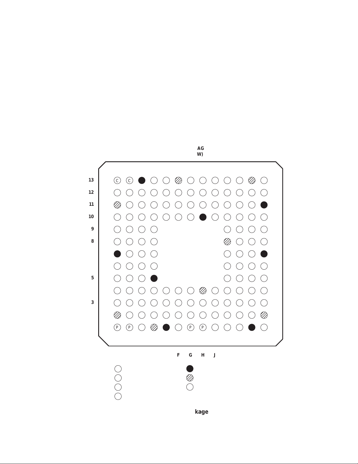
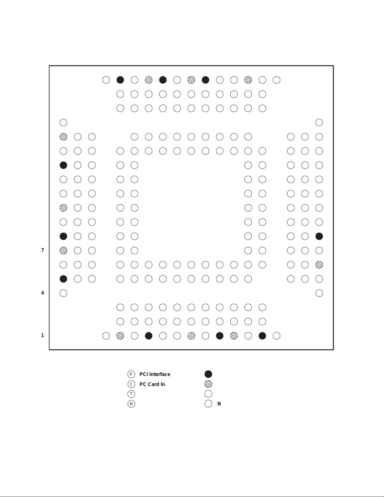
The PCI1510 controller is available in five packages, a 144-terminal quad flatpack (PGE), two 144-terminal MicroStar
BGA packages (GGU/ZGU), and two 209-terminal PBGA packages (GVF/ZVF). The GGU and ZGU packages are
mechanically and electrically identical, but the ZGU is a lead-free (Pb, atomic number 82) design. Throughout the
remainder of this manual, only the GGU package designator is used for either the GGU or ZGU package. The terminal
layout for the GGU package is shown in Figure 2−1. The GVF and ZVF packages are mechanically and electrically
identical, but the ZVF is a lead-free (Pb, atomic number 82) design. Throughout the remainder of this manual, only
the GVF package designator is used for either the GVF or ZVF package. The terminal layout for the GVF package
is shown in Figure 2−2. The terminal layout with signal names for the PGE package is shown in Figure 2−3.
GGU PACKAGE
(TOP VIEW)
13
12
10
CC CC CCCCC T
CC CC CCCCT MCCC
11
9
8
7
6
5
4
3
2
1
C CC CCCCCTC
CC CC C CMMCMC
CC C TM MC
CC C PC
CC MPPC
CC C PP PPC
CC PP PPC
CC PPPPPPPPC
CC PP PPPPP PPPP
C PP PPPPPPPP
PP PPPPP PPP
A
P
PCI Interface
C
PC Card Interface
T
TPS Power Switch
M
MFUNC Pins
DB C
E
HJFG
VCC
Ground (GND)
Miscellaneous
MNKL
Figure 2−1. PCI1510 GGU-Package Terminal Diagram
2−1
GVF PACKAGE
(TOP VIEW)
19
18
17
16
15
14
13
12
11
10
N
C
C
C
C
C
C
C
C
C
C
C
C
C
C
C
C
C
C
C
9
8
C
C
C
7
C
C
C
C
C
C
C
C
C
C
C
C
C
C
C
C
C
C
C
C
C
C
C
C
NNNN
C
C
C
C
C
C
C
C
C
C
C
C
C
C
C
C
N
N
N
N
N
N
N
N
N
N
N
N
N
N
N
N
N
N
P
P
NN
N
N
N
N
N
N
N
N
N
N
N
P
P
P
N
N
N
N
N
N
N
N
N
N
N
N
N
N
N
P
P
P
P
P
P
P
P
6
5
4
T
NNN
TT
3
2
1
N
N
T
N
N
M
M
M
P
PCI Interface
C
PC Card Interface
T
TPS Power Switch
M
MFUNC Pins
M
M
MM
P
P
P
P
P
P
P
P
P
P
P
P
P
P
P
P
P
P
P
P
P
P
P
P
MNKLHJFGDBCAE
P
P
P
P
P
P
P
P
P
PR WTUV
P
P
P
P
P
P
VCC
Ground (GND)
Miscellaneous
N
No Connection
Figure 2−2. PCI1510 GVF-Package Terminal Diagram
2−2
2.1 PCI1510 Terminal Assignments
PGE PACKAGE
Figure 2−3 and Table 2−1 show the terminal assignments for the PGE package. Table 2−2 and Table 2−3 list the
terminal assignments for the GGU and GVF packages, respectively. The signal names for the PC Card slot are given
in a CardBus // 16-bit signal format. All tables are arranged in order by increasing terminal designator, which is
numeric for the PGE package and alphanumeric for the other packages. Table 2−4 and Table 2−5 list the CardBus
and 16-bit signal names, respectively, in alphanumerical order with the corresponding terminal numbers for each
package.
(TOP VIEW)
VCCCB
CIRDY
CFRAME
CC/BE2//A12
CAD17//A24
CAD18//A7
CAD19//A25
CVS2//VS2
CAD20//A6
//RESET
CRST
CAD21//A5
CAD22//A4
CREQ
//INPACK
CAD23//A3
CC/BE3
VR_EN
CAD24//A2
CAD25//A1
CAD26//A0
CVS1//VS1
CINT//READY(IREQ)
CSERR//WAIT
CAUDIO//BVD2(SPKR)
CSTSCHG//BVD1(STSCHG
CCLKRUN
//WP(IOIS16)
CCD2
CAD27//D0
CAD28//D8
CAD29//D1
CAD30//D9
CRSVD//D2
CAD31//D10
//A15
//A23
GND
//REG
VCC
GND
/RI)
VCC
//CD2
//A21
//A22
//WE
CCLK//A16
CDEVSEL
CTRDY
CGNT
105
106
107
108
109
110
111
112
113
114
115
116
117
118
119
120
121
122
123
124
125
126
127
128
129
130
131
132
133
134
135
136
137
138
139
140
141
142
143
144
1234567891011121314151617181920212223242526272829303132333435
//A19
//A14
//A20
VCC
CSTOP
CBLOCK
CPERR
101
102
103
104
CPAR//A13
CRSVD//A18
99
100
//A8
CAD16//A17
CC/BE1
97
98
CAD14//A9
CAD15//IOWR
CAD13//IORD
94
95
96
GND
93
CAD12//A11
92
CAD11//OE
CAD10//CE2
90
91
//CE1
CAD9//A10
CC/BE0
CAD8//D15
87
88
89
CAD7//D7
CLK_48_RSVD
CRSVD//D14
84
85
86
CAD5//D6
CAD6//D13
CAD3//D5
81
82
83
GND
CAD4//D12
79
80
CAD1//D4
78
CAD2//D11
CAD0//D3
76
77
//CD1
CCD1
75
VCCD1
VCCD0
73
74
36
72
VPPD1
71
VPPD0
70
VCC
69
MFUNC6
68
MFUNC5
67
MFUNC4
66
GRST
65
SUSPEND
64
MFUNC3
63
MFUNC2
62
VR_PORT
61
SPKROUT
60
GND
59
MFUNC1
58
MFUNC0
57
56
55
54
53
52
51
50
49
48
47
46
45
44
43
42
41
40
39
38
37
RI_OUT
AD0
AD1
VCC
AD2
AD3
AD4
AD5
AD6
AD7
C/BE0
AD8
AD9
AD10
AD11
AD12
AD13
GND
AD14
AD15
C/BE1
/PME
REQ
GNT
AD31
AD30
AD29
AD28
AD27
GND
AD26
AD25
AD24
VCC
C/BE3
IDSEL
AD23
AD22
AD21
AD20
PRST
PCLK
GND
AD19
AD18
AD17
AD16
C/BE2
FRAME
IRDY
Figure 2−3. PCI1510 PGE-Package Terminal Diagram
TRDY
STOP
DEVSEL
VCC
SERR
PERR
PAR
VCCP
2−3

Table 2−1. Signal Names Sorted by PGE Terminal Number
TERMINAL
TERMINAL
SIGNAL NAME
CARDBUS 16-BIT
1 REQ REQ 43 AD11 AD11
2 GNT GNT 44 AD10 AD10
3 AD31 AD31 45 AD9 AD9
4 AD30 AD30 46 AD8 AD8
5 AD29 AD29 47 C/BE0 C/BE0
6 AD28 AD28 48 AD7 AD7
7 AD27 AD27 49 AD6 AD6
8 GND GND 50 AD5 AD5
9 AD26 AD26 51 AD4 AD4
10 AD25 AD25 52 AD3 AD3
11 AD24 AD24 53 AD2 AD2
12 V
13 C/BE3 C/BE3 55 AD1 AD1
14 IDSEL IDSEL 56 AD0 AD0
15 AD23 AD23 57 RI_OUT/PME RI_OUT/PME
16 AD22 AD22 58 MFUNC0 MFUNC0
17 AD21 AD21 59 MFUNC1 MFUNC1
18 AD20 AD20 60 GND GND
19 PRST PRST 61 SPKROUT SPKROUT
20 PCLK PCLK 62 VR_PORT VR_PORT
21 GND GND 63 MFUNC2 MFUNC2
22 AD19 AD19 64 MFUNC3 MFUNC3
23 AD18 AD18 65 SUSPEND SUSPEND
24 AD17 AD17 66 GRST GRST
25 AD16 AD16 67 MFUNC4 MFUNC4
26 C/BE2 C/BE2 68 MFUNC5 MFUNC5
27 FRAME FRAME 69 MFUNC6 MFUNC6
28 IRDY IRDY 70 V
29 TRDY TRDY 71 VPPD0 VPPD0
30 DEVSEL DEVSEL 72 VPPD1 VPPD1
31 STOP STOP 73 VCCD0 VCCD0
32 V
33 PERR PERR 75 CCD1 CD1
34 SERR SERR 76 CAD0 D3
35 PAR PAR 77 CAD2 D11
36 V
37 C/BE1 C/BE1 79 CAD4 D12
38 AD15 AD15 80 GND GND
39 AD14 AD14 81 CAD3 D5
40 GND GND 82 CAD6 D13
41 AD13 AD13 83 CAD5 D6
42 AD12 AD12 84 CRSVD D14
CC
CC
CCP
V
V
V
CC
CC
CCP
54 V
74 VCCD1 VCCD1
78 CAD1 D4
CARDBUS 16-BIT
CC
CC
SIGNAL NAME
V
CC
V
CC
2−4

Table 2−1. Signal Names Sorted by PGE Terminal Number (Continued)
TERMINAL
TERMINAL
SIGNAL NAME
CARDBUS 16-BIT
85† CLK_48_RSVD CLK_48_RSVD 115 CAD18 A7
86 CAD7 D7 116 CAD19 A25
87 CAD8 D15 117 CVS2 VS2
88 CC/BE0 CE1 118 CAD20 A6
89 CAD9 A10 119 CRST RESET
90 CAD10 CE2 120 CAD21 A5
91 CAD11 OE 121 CAD22 A4
92 CAD12 A11 122 CREQ INPACK
93 GND GND 123 CAD23 A3
94 CAD13 IORD 124 CC/BE3 REG
95 CAD15 IOWR 125 VR_EN VR_EN
96 CAD14 A9 126 V
97 CAD16 A17 127 CAD24 A2
98 CC/BE1 A8 128 CAD25 A1
99 CRSVD A18 129 CAD26 A0
100 CPAR A13 130 CVS1 VS1
101 CBLOCK A19 131 CINT READY(IREQ)
102 CPERR A14 132 GND GND
103 CSTOP A20 133 CSERR WAIT
104 V
105 CGNT WE 135 CSTSCHG BVD1(STSCHG/RI)
106 CDEVSEL A21 136 CCLKRUN WP(IOIS16)
107 CCLK A16 137 V
108 CTRDY A22 138 CCD2 CD2
109 V
110 CIRDY A15 140 CAD28 D8
111 CFRAME A23 141 CAD29 D1
112 GND GND 142 CAD30 D9
113 CC/BE2 A12 143 CRSVD D2
114 CAD17 A24 144 CAD31 D10
†
Terminal 85 is an NC on the PCI1510 to allow for terminal compatibility with the next generation of devices.
CC
CCCB
V
CC
V
CCCB
134 CAUDIO BVD2(SPKR)
139 CAD27 D0
CARDBUS 16-BIT
CC
CC
SIGNAL NAME
V
CC
V
CC
2−5

Table 2−2. Signal Names Sorted by GGU Terminal Number
TERMINAL
TERMINAL
SIGNAL NAME
CARDBUS 16-BIT
A01 C/BE3 C/BE3 D05 V
A02 GND GND D06 CAUDIO BVD2(SPKR)
A03 CRSVD D2 D07 CAD25 A1
A04 CAD27 D0 D08 CRST RESET
A05 CCLKRUN WP(IOIS16) D09 CC/BE2 A12
A06 CINT READY(IREQ) D10 CAD23 A3
A07 V
A08 CC/BE3 REG D12 CPERR A14
A09 CVS2 VS2 D13 CGNT WE
A10 CFRAME A23 E01 V
A11 GND GND E02 AD25 AD25
A12 CAD18 A7 E03 AD31 AD31
A13 CBLOCK A19 E04 AD29 AD29
B01 AD27 AD27 E10 CSTOP A20
B02 CVS1 VS1 E11 CC/BE1 A8
B03 CAD31 D10 E12 CPAR A13
B04 CAD30 D9 E13 CRSVD A18
B05 CCD2 CD2 F01 AD22 AD22
B06 CSERR WAIT F02 IDSEL IDSEL
B07 CAD24 A2 F03 AD24 AD24
B08 CREQ INPACK F04 AD26 AD26
B09 CAD19 A25 F10 CAD16 A17
B10 CAD17 A24 F11 CAD14 A9
B11 V
B12 CAD22 A4 F13 GND GND
B13 CCLK A16 G01 PCLK PCLK
C01 GNT GNT G02 AD20 AD20
C02 REQ REQ G03 PRST PRST
C03 AD23 AD23 G04 AD21 AD21
C04 CAD29 D1 G10 CAD11 OE
C05 CAD28 D8 G11 CAD9 A10
C06 CSTSCHG BVD1(STSCHG/RI) G12 CAD12 A11
C07 CAD26 A0 G13 CAD10 CE2
C08 CAD21 A5 H01 AD17 AD17
C09 CAD20 A6 H02 AD19 AD19
C10 CIRDY A15 H03 AD18 AD18
C11 CAD15 IOWR H04 GND GND
C12 CTRDY A22 H10† CLK_48_RSVD CLK_48_RSVD
C13 V
D01 GND GND H12 CAD7 D7
D02 AD28 AD28 H13 CC/BE0 CE1
D03 AD30 AD30 J01 FRAME FRAME
D04 VR_EN VR_EN J02 C/BE2 C/BE2
†
Terminal H10 is not bonded out in the packaged parts in order to have pin compatibility with future devices.
CC
CCCB
CC
V
CC
V
CCCB
V
CC
D11 CDEVSEL A21
F12 CAD13 IORD
H11 CAD8 D15
CARDBUS 16-BIT
CC
CC
SIGNAL NAME
V
CC
V
CC
2−6

Table 2−2. Signal Names Sorted by GGU Terminal Number (Continued)
TERMINAL
TERMINAL
SIGNAL NAME
CARDBUS 16-BIT
J03 TRDY TRDY L11 GRST GRST
J04 AD16 AD16 L12 VCCD1 VCCD1
J10 CAD5 D6 L13 CCD1 CD1
J11 CAD4 D12 M01 V
J12 CRSVD D14 M02 AD9 AD9
J13 CAD3 D5 M03 C/BE1 C/BE1
K01 IRDY IRDY M04 AD15 AD15
K02 DEVSEL DEVSEL M05 AD10 AD10
K03 PERR PERR M06 AD5 AD5
K04 AD4 AD4 M07 AD1 AD1
K05 AD13 AD13 M08 RI_OUT/PME RI_OUT/PME
K06 C/BE0 C/BE0 M09 SPKROUT SPKROUT
K07 MFUNC0 MFUNC0 M10 MFUNC4 MFUNC4
K08 GND GND M11 VPPD1 VPPD1
K09 VPPD0 VPPD0 M12 CAD2 D11
K10 MFUNC3 MFUNC3 M13 GND GND
K11 CAD0 D3 N01 PAR PAR
K12 CAD1 D4 N02 GND GND
K13 CAD6 D13 N03 AD12 AD12
L01 STOP STOP N04 AD8 AD8
L02 SERR SERR N05 AD7 AD7
L03 V
L04 AD11 AD11 N07 V
L05 AD14 AD14 N08 AD0 AD0
L06 AD6 AD6 N09 MFUNC1 MFUNC1
L07 AD2 AD2 N10 SUSPEND SUSPEND
L08 VR_PORT VR_PORT N11 V
L09 MFUNC2 MFUNC2 N12 MFUNC5 MFUNC5
L10 MFUNC6 MFUNC6 N13 VCCD0 VCCD0
CCP
V
CCP
N06 AD3 AD3
CARDBUS 16-BIT
CC
CC
CC
SIGNAL NAME
V
CC
V
CC
V
CC
2−7

Table 2−3. Signal Names Sorted by GVF Terminal Number
TERMINAL
TERMINAL
SIGNAL NAME
CARDBUS 16-BIT
A04 VPPD0 VPPD0 E07 NC NC
A05 V
A06 NC NC E09 CAD28 D8
A07 GND GND E10 CSERR WAIT
A08 V
A09 CSTSCHG BVD1(STSCHG/RI) E12 CAD21 A5
A10 GND GND E13 CAD18 A7
A11 V
A12 CAD23 A3 E17 CSTOP A20
A13 V
A14 CAD19 A25 E19 V
A15 GND GND F01 MFUNC5 MFUNC5
A16 CDEVSEL A21 F02 MFUNC3 MFUNC3
B05 VCCD1 VCCD1 F03 MFUNC2 MFUNC2
B06 NC NC F05 MFUNC0 MFUNC0
B07 NC NC F06 NC NC
B08 CAD29 D1 F07 NC NC
B09 CCLKRUN WP(IOIS16) F08 CRSVD D2
B10 CVS1 VS1 F09 CAD27 D0
B11 CC/BE3 REG F10 CAUDIO BVD2(SPKR)
B12 CREQ INPACK F11 CAD26 A0
B13 CRST RESET F12 CVS2 VS2
B14 CAD17 A24 F13 CIRDY A15
B15 CFRAME A23 F14 CPAR A13
C05 VPPD1 VPPD1 F15 CPERR A14
C06 NC NC F17 CRSVD A18
C07 NC NC F18 CAD16 A17
C08 CAD30 D9 F19 CAD14 A9
C09 CCD2 CD2 G01 V
C10 CINT READY(IREQ) G02 VR_PORT VR_PORT
C11 CAD24 A2 G03 SUSPEND SUSPEND
C12 CAD22 A4 G05 MFUNC4 MFUNC4
C13 CAD20 A6 G06 MFUNC1 MFUNC1
C14 CC/BE2 A12 G14 V
C15 CCLK A16 G15 CC/BE1 A8
D01 NC NC G17 CAD15 IOWR
D19 CGNT WE G18 CAD13 IORD
E01 GND GND G19 GND GND
E02 SPKROUT SPKROUT H01 PCLK PCLK
E03 NC NC H02 GRST GRST
E05 NC NC H03 PRST PRST
E06 VCCD0 VCCD0 H05 VR_EN VR_EN
†
Terminal F06 is not bonded out in the packaged parts in order to have pin compatibility with future devices.
CC
CC
CCCB
CC
V
CC
V
CC
V
CCCB
V
CC
E08 CAD31 D10
E11 CAD25 A1
E14 CTRDY A22
E18 CBLOCK A19
CARDBUS 16-BIT
CC
CC
CCCB
SIGNAL NAME
V
CC
V
CC
V
CCCB
2−8

Table 2−3. Signal Names Sorted by GVF Terminal Number (Continued)
TERMINAL
TERMINAL
SIGNAL NAME
CARDBUS 16-BIT
H06 MFUNC6 MFUNC6 M17 NC NC
H14 CAD11 OE M18 NC NC
H15 CAD12 A11 M19 NC NC
H17 CAD10 CE2 N01 GND GND
H18 CAD9 A10 N02 AD19 AD19
H19 V
J01 GNT GNT N05 FRAME FRAME
J02 REQ REQ N06 AD17 AD17
J03 RI_OUT/PME RI_OUT/PME N14 NC NC
J05 AD31 AD31 N15 NC NC
J06 AD30 AD30 N17 NC NC
J14 CAD8 D15 N18 NC NC
J15 CC/BE0 CE1 N19 NC NC
J17 CAD7 D7 P01 AD16 AD16
J18 CRSVD D14 P02 C/BE2 C/BE2
J19 CAD5 D6 P03 IRDY IRDY
K01 GND GND P05 STOP STOP
K02 AD29 AD29 P06 TRDY TRDY
K03 AD28 AD28 P07 AD14 AD14
K05 AD27 AD27 P08 AD9 AD9
K06 AD26 AD26 P09 NC NC
K14 CAD6 D13 P10 NC NC
K15 CAD3 D5 P11 NC NC
K17 CAD4 D12 P12 NC NC
K18 CAD1 D4 P13 NC NC
K19 GND GND P14 NC NC
L01 V
L02 AD25 AD25 P17 NC NC
L03 AD24 AD24 P18 NC NC
L05 IDSEL IDSEL P19 GND GND
L06 C/BE3 C/BE3 R01 V
L14 CAD2 D11 R02 DEVSEL DEVSEL
L15 CAD0 D3 R03 PERR PERR
L17 CCD1 CD1 R06 AD15 AD15
L18 VR_PORT VR_PORT R07 AD10 AD10
L19 V
M01 V
M02 AD23 AD23 R10 NC NC
M03 AD22 AD22 R11 NC NC
M05 AD20 AD20 R12 NC NC
M06 AD21 AD21 R13 NC NC
M14 NC NC R14 NC NC
M15 NC NC R17 NC NC
CC
CCP
CC
CC
V
V
V
V
CC
CCP
CC
CC
N03 AD18 AD18
P15 NC NC
R08 AD6 AD6
R09 AD0 AD0
CARDBUS 16-BIT
CC
SIGNAL NAME
V
CC
2−9

Table 2−3. Signal Names Sorted by GVF Terminal Number (Continued)
TERMINAL
TERMINAL
SIGNAL NAME
CARDBUS 16-BIT
R18 NC NC V10 NC NC
R19 NC NC V11 NC NC
T01 SERR SERR V12 NC NC
T19 NC NC V13 NC NC
U05 C/BE1 C/BE1 V14 NC NC
U06 AD12 AD12 V15 NC NC
U07 AD8 AD8 W04 PAR PAR
U08 AD5 AD5 W05 V
U09 AD1 AD1 W06 GND GND
U10 NC NC W07 AD7 AD7
U11 NC NC W08 V
U12 NC NC W09 AD3 AD3
U13 NC NC W10 NC NC
U14 NC NC W11 NC NC
U15 NC NC W12 NC NC
V05 AD13 AD13 W13 NC NC
V06 AD11 AD11 W14 NC NC
V07 C/BE0 C/BE0 W15 NC NC
V08 AD4 AD4 W16 NC NC
V09 AD2 AD2
CARDBUS 16-BIT
CCP
CC
SIGNAL NAME
V
CCP
V
CC
2−10

Table 2−4. CardBus PC Card Signal Names Sorted Alphabetically to Device Terminals
SIGNAL NAME
SIGNAL NAME
TERMINAL
PGE GGU GVF
AD0 56 N08 R09 CAD11 91 G10 H14
AD1 55 M07 U09 CAD12 92 G12 H15
AD2 53 L07 V09 CAD13 94 F12 G18
AD3 52 N06 W09 CAD14 96 F11 F19
AD4 51 K04 V08 CAD15 95 C11 G17
AD5 50 M06 U08 CAD16 97 F10 F18
AD6 49 L06 R08 CAD17 114 B10 B14
AD7 48 N05 W07 CAD18 115 A12 E13
AD8 46 N04 U07 CAD19 116 B09 A14
AD9 45 M02 P08 CAD20 118 C09 C13
AD10 44 M05 R07 CAD21 120 C08 E12
AD11 43 L04 V06 CAD22 121 B12 C12
AD12 42 N03 U06 CAD23 123 D10 A12
AD13 41 K05 V05 CAD24 127 B07 C11
AD14 39 L05 P07 CAD25 128 D07 E11
AD15 38 M04 R06 CAD26 129 C07 F11
AD16 25 J04 P01 CAD27 139 A04 F09
AD17 24 H01 N06 CAD28 140 C05 E09
AD18 23 H03 N03 CAD29 141 C04 B08
AD19 22 H02 N02 CAD30 142 B04 C08
AD20 18 G02 M05 CAD31 144 B03 E08
AD21 17 G04 M06 CAUDIO 134 D06 F10
AD22 16 F01 M03 C/BE0 47 K06 V07
AD23 15 C03 M02 C/BE1 37 M03 U05
AD24 11 F03 L03 C/BE2 26 J02 P02
AD25 10 E02 L02 C/BE3 13 A01 L06
AD26 9 F04 K06 CBLOCK 101 A13 E18
AD27 7 B01 K05 CC/BE0 88 H13 J15
AD28 6 D02 K03 CC/BE1 98 E11 G15
AD29 5 E04 K02 CC/BE2 113 D09 C14
AD30 4 D03 J06 CC/BE3 124 A08 B11
AD31 3 E03 J05 CCD1 75 L13 L17
CAD0 76 K11 L15 CCD2 138 B05 C09
CAD1 78 K12 K18 CCLK 107 B13 C15
CAD2 77 M12 L14 CCLKRUN 136 A05 B09
CAD3 81 J13 K15 CDEVSEL 106 D11 A16
CAD4 79 J11 K17 CFRAME 111 A10 B15
CAD5 83 J10 J19 CGNT 105 D13 D19
CAD6 82 K13 K14 CINT 131 A06 C10
CAD7 86 H12 J17 CIRDY 110 C10 F13
CAD8 87 H11 J14 CLK_48_RSVD 85 H10 —
CAD9 89 G11 H18 CPAR 100 E12 F14
CAD10 90 G13 H17 CPERR 102 D12 F15
PGE GGU GVF
TERMINAL
2−11

Table 2−4. CardBus PC Card Signal Names Sorted Alphabetically to Device Terminals (Continued)
SIGNAL NAME
SIGNAL NAME
TERMINAL
PGE GGU GVF
CREQ 122 B08 B12 MFUNC4 67 M10 G05
CRST 119 D08 B13 MFUNC5 68 N12 F01
CRSVD 84 A03 F08 MFUNC6 69 L10 H06
CRSVD 99 E13 F17 PAR 35 N01 W04
CRSVD 143 J12 J18 PCLK 20 G01 H01
CSERR 133 B06 E10 PERR 33 K03 R03
CSTOP 103 E10 E17 PRST 19 G03 H03
CSTSCHG 135 C06 A09 REQ 1 C02 J02
CTRDY 108 C12 E14 RI_OUT/PME 57 M08 J03
CVS1 130 B02 B10 SERR 34 L02 T01
CVS2 117 A09 F12 SPKROUT 61 M09 E02
DEVSEL 30 K02 R02 STOP 31 L01 P05
FRAME 27 J01 N05 SUSPEND 65 N10 G03
GNT 2 C01 J01 TRDY 29 J03 P06
GRST 66 L11 H02 VCCD0 73 N13 E06
IDSEL 14 F02 L05 VCCD1 74 L12 B05
IRDY 28 K01 P03 VPPD0 71 K09 A04
MFUNC0 58 K07 F05 VPPD1 72 M11 C05
MFUNC1 59 N09 G06 VR_EN 125 D04 H05
MFUNC2 63 L09 F03 VR_PORT 62 L08 G02, L18
MFUNC3 64 K10 F02
PGE GGU GVF
TERMINAL
2−12

Table 2−5. 16-Bit PC Card Signal Names Sorted Alphabetically to Device Terminals
SIGNAL NAME
SIGNAL NAME
TERMINAL
PGE GGU GVF
AD0 56 N08 R09 A11 92 G12 H15
AD1 55 M07 U09 A12 113 D09 C14
AD2 53 L07 V09 A13 100 E12 F14
AD3 52 N06 W09 A14 102 D12 F15
AD4 51 K04 V08 A15 110 C10 F13
AD5 50 M06 U08 A16 107 B13 C15
AD6 49 L06 R08 A17 97 F10 F18
AD7 48 N05 W07 A18 99 E13 F17
AD8 46 N04 U07 A19 101 A13 E18
AD9 45 M02 P08 A20 103 E10 E17
AD10 44 M05 R07 A21 106 D11 A16
AD11 43 L04 V06 A22 108 C12 E14
AD12 42 N03 U06 A23 111 A10 B15
AD13 41 K05 V05 A24 114 B10 B14
AD14 39 L05 P07 A25 116 B09 A14
AD15 38 M04 R06 BVD1(STSCHG/RI) 135 C06 A09
AD16 25 J04 P01 BVD2(SPKR) 134 D06 F10
AD17 24 H01 N06 C/BE0 47 K06 V07
AD18 23 H03 N03 C/BE1 37 M03 U05
AD19 22 H02 N02 C/BE2 26 J02 P02
AD20 18 G02 M05 C/BE3 13 A01 L06
AD21 17 G04 M06 CD1 75 L13 L17
AD22 16 F01 M03 CD2 138 B05 C09
AD23 15 C03 M02 CE1 88 H13 J15
AD24 11 F03 L03 CE2 90 G13 H17
AD25 10 E02 L02 CLK_48_RSVD 85 H10 —
AD26 9 F04 K06 DEVSEL 30 K02 R02
AD27 7 B01 K05 D0 139 A04 F09
AD28 6 D02 K03 D1 141 C04 B08
AD29 5 E04 K02 D2 143 A03 F08
AD30 4 D03 J06 D3 76 K11 L15
AD31 3 E03 J05 D4 78 K12 K18
A0 129 C07 F11 D5 81 J13 K15
A1 128 D07 E11 D6 83 J10 J19
A2 127 B07 C11 D7 86 H12 J17
A3 123 D10 A12 D8 140 C05 E09
A4 121 B12 C12 D9 142 B04 C08
A5 120 C08 E12 D10 144 B03 E08
A6 118 C09 C13 D11 77 M12 L14
A7 115 A12 E13 D12 79 J11 K17
A8 98 E11 G15 D13 82 K13 K14
A9 96 F11 F19 D14 84 J12 J18
A10 89 G11 H18 D15 87 H11 J14
PGE GGU GVF
TERMINAL
2−13

Table 2−5. 16-Bit PC Card Signal Names Sorted Alphabetically to Device Terminals (Continued)
SIGNAL NAME
SIGNAL NAME
TERMINAL
PGE GGU GVF
FRAME 27 J01 N05 REG 124 A08 B11
GNT 2 C01 J01 REQ 1 C02 J02
GRST 66 L11 H02 RESET 119 D08 B13
IDSEL 14 F02 L05 RI_OUT/PME 57 M08 J03
INPACK 122 B08 B12 SERR 34 L02 T01
IORD 94 F12 G18 SPKROUT 61 M09 E02
IOWR 95 C11 G17 STOP 31 L01 P05
IRDY 28 K01 P03 SUSPEND 65 N10 G03
MFUNC0 58 K07 F05 TRDY 29 J03 P06
MFUNC1 59 N09 G06 VCCD0 73 N13 E06
MFUNC2 63 L09 F03 VCCD1 74 L12 B05
MFUNC3 64 K10 F02 VPPD0 71 K09 A04
MFUNC4 67 M10 G05 VPPD1 72 M11 C05
MFUNC5 68 N12 F01 VR_EN 125 D04 H05
MFUNC6 69 L10 H06 VR_PORT 62 L08 G02, L18
OE 91 G10 H14 VS1 130 B02 B10
PAR 35 N01 W04 VS2 117 A09 F12
PCLK 20 G01 H01 WAIT 133 B06 E10
PERR 33 K03 R03 WE 105 D13 D19
PRST 19 G03 H03 WP(IOIS16) 136 A05 B09
READY(IREQ) 131 A06 C10
PGE GGU GVF
TERMINAL
2−14
2.2 Terminal Descriptions
NAME
I/O
DESCRIPTION
NAME
I/O
DESCRIPTION
The terminals are grouped in tables by functionality, such as PCI system function, power-supply function, etc. The
terminal numbers are also listed for convenient reference.
Table 2−6. Power Supply Terminals
TERMINAL
NUMBER
PGE GGU GVF
8, 21, 40,
GND
V
CC
V
CCCB
V
CCP
VR_EN 125 D04 H05 I Internal voltage regulator enable. Active-low
VR_PORT 62 L08 G02, L18
60, 80, 93,
112, 132
12, 32, 54,
70, 104,
126, 137
109 B11 A11, G14
36 L03 L01, W05 Clamp voltage for PCI and miscellaneous I/O, 5 V or 3.3 V
A02, A11, D01,
F13, H04, K08,
M13, N02
A07, C13, D05,
E01, M01, N07,
N11
A07, A10, A15,
E01, G19, K01,
K19, N01, P19,
W06
A05, A08, A13,
E19, G01, H19,
L19, M01, R01,
W08
I/O DESCRIPTION
Device ground terminals
Power supply terminals for I/O and internal voltage regulator
Clamp voltage for PC Card interface. Matches card signaling
environment, 5 V or 3.3 V
Internal voltage regulator input/output. When VR_EN is low, the
regulator is enabled and this terminal is an output. An external
bypass capacitor is required on this terminal. When VR_EN is high,
the regulator is disabled and this terminal is an input for an external
2.5-V core power source.
VCCD0
VCCD1
VPPD0
VPPD1
TERMINAL
NUMBER
PGE GGU GVF
73
74
71
72
N13
L12
K09
M11
E06
B05
A04
C05
Table 2−7. PC Card Power Switch Terminals
I/O DESCRIPTION
O Logic controls to the TPS2211A PC Card power interface switch to control AVCC
O Logic controls to the TPS2211A PC Card power interface switch to control AVPP
2−15
TERMINAL
NAME
I/O
DESCRIPTION
NUMBER
PGE GGU GVF
GRST 66 L11 H02 I
PCLK 20 G01 H01 I
PRST 19 G03 H03 I
Table 2−8. PCI System Terminals
I/O DESCRIPTION
Global reset. When the global reset is asserted, the GRST signal causes the controller to
place all output buffers in a high-impedance state and reset all internal registers. When GRST
is asserted, the device is completely in its default state. For systems that require wake-up
from D3, GRST
initial boot so that PME context is retained during the transition from D3 to D0.
When the SUSPEND
registers are preserved. All outputs are placed in a high-impedance state.
PCI bus clock. PCLK provides timing for all transactions on the PCI bus. All PCI signals are
sampled at the rising edge of PCLK.
PCI bus reset. When the PCI bus reset is asserted, PRST causes the controller to place all
output buffers in a high-impedance state and reset internal registers. When PRST
the device can generate the PME
controller is in a default state.
When the SUSPEND
registers are preserved. All outputs are placed in a high-impedance state.
normally is asserted only during initial boot. PRST must be asserted following
mode is enabled, the device is protected from GRST, and the internal
signal only if it is enabled. After PRST is deasserted, the
mode is enabled, the device is protected from PRST, and the internal
is asserted,
2−16

TERMINAL
NAME
I/O
DESCRIPTION
NUMBER
PGE GGU GVF
AD31
AD30
AD29
AD28
AD27
AD26
AD25
AD24
AD23
AD22
AD21
AD20
AD19
AD18
AD17
AD16
AD15
AD14
AD13
AD12
AD11
AD10
AD9
AD8
AD7
AD6
AD5
AD4
AD3
AD2
AD1
AD0
C/BE3
C/BE2
C/BE1
C/BE0
PAR 35 N01 W04 I/O
10
11
15
16
17
18
22
23
24
25
38
39
41
42
43
44
45
46
48
49
50
51
52
53
55
56
13
26
37
47
3
E03
J05
4
D03
J06
5
E04
K02
6
D02
K03
7
B01
K05
9
F04
K06
E02
L02
F03
L03
C03
M02
F01
M03
G04
M06
G02
M05
H02
N02
H03
N03
H01
N06
J04
P01
M04
R06
L05
P07
K05
N03
M05
M02
N04
N05
M06
K04
N06
M07
N08
A01
M03
K06
L04
L06
L07
J02
V05
U06
V06
R04
P08
U07
W07
R08
U08
V08
W09
V09
U09
R09
L06
P02
U05
V07
Table 2−9. PCI Address and Data Terminals
I/O DESCRIPTION
PCI address/data bus. These signals make up the multiplexed PCI address and data bus on the
primary interface. During the address phase of a primary-bus PCI cycle, AD31–AD0 contain a
I/O
32-bit address or other destination information. During the data phase, AD31–AD0 contain data.
PCI-bus commands and byte enables. These signals are multiplexed on the same PCI
terminals. During the address phase of a primary-bus PCI cycle, C/BE3
command. During the data phase, this 4-bit bus is used as a byte enable. The byte enable
I/O
determines which byte paths of the full 32-bit data bus carry meaningful data. C/BE0 applies to
byte 0 (AD7–AD0), C/BE1
(AD23–AD16), and C/BE3
PCI-bus parity. In all PCI-bus read and write cycles, the controller calculates even parity across
the AD31–AD0 and C/BE3
this parity indicator with a one-PCLK delay. As a target during PCI cycles, the controller
compares its calculated parity to the parity indicator of the initiator. A compare error results in the
assertion of a parity error (PERR
applies to byte 1 (AD15–AD8), C/BE2 applies to byte 2
applies to byte 3 (AD31–AD24).
–C/BE0 buses. As an initiator during PCI cycles, the controller outputs
).
–C/BE0 define the bus
2−17
Table 2−10. PCI Interface Control Terminals
NAME
I/O
DESCRIPTION
TERMINAL
NUMBER
PGE GGU GVF
DEVSEL 30 K02 R02 I/O
FRAME 27 J01 N05 I/O
GNT 2 C01 J01 I
IDSEL 14 F02 L05 I
IRDY 28 K01 P03 I/O
PERR 33 K03 R03 I/O
REQ 1 C02 J02 O
SERR 34 L02 T01 O
STOP 31 L01 P05 I/O
TRDY 29 J03 P06 I/O
I/O DESCRIPTION
PCI device select. The controller asserts DEVSEL to claim a PCI cycle as the target device.
As a PCI initiator on the bus, the controller monitors DEVSEL
target responds before timeout occurs, then the controller terminates the cycle with an initiator
abort.
PCI cycle frame. FRAME is driven by the initiator of a bus cycle. FRAME is asserted to indicate
that a bus transaction is beginning, and data transfers continue while this signal is asserted.
When FRAME
PCI bus grant. GNT is driven by the PCI bus arbiter to grant the controller access to the PCI
bus after the current data transaction has completed. GNT
request, depending on the PCI bus parking algorithm.
Initialization devic e s e l e c t . I D S E L s e l e c t s th e con trol ler d uri ng configuration space accesses.
IDSEL can be connected to one of the upper 24 PCI address lines on the PCI bus.
PCI initiator ready. IRDY indicates the ability of the PCI bus initiator to complete the current
data phase of the transaction. A data phase is completed on a rising edge of PCLK where both
IRDY and TRDY are asserted. Until IRDY and TRDY are both sampled asserted, wait states
are inserted.
PCI parity error indicator. PERR is driven by a PCI device to indicate that calculated parity
does not match P AR when PERR
04h, see Section 4.4).
PCI bus request. REQ is asserted by the controller to request access to the PCI bus as an
initiator.
PCI system error. SERR is an output that is pulsed from the controller when enabled through
bit 8 of the command register (PCI offset 04h, see Section 4.4) indicating a system error has
occurred. The controller need not be the target of the PCI cycle to assert this signal. When
SERR
parity error has occurred on a CardBus interface.
PCI cycle stop signal. STOP is driven by a PCI target to request the initiator to stop the current
PCI bus transaction. STOP
devices that do not support burst data transfers.
PCI target ready. TRDY indicates the ability of the primary bus target to complete the current
data phase of the transaction. A data phase is completed on a rising edge of PCLK when both
IRDY and TRDY are asserted. Until both IRDY and TRDY are asserted, wait states are
inserted.
is deasserted, the PCI bus transaction is in the final data phase.
is enabled through bit 6 of the command register (PCI offset
is enabled in the command register, this signal also pulses, indicating that an address
is used for target disconnects and is commonly asserted by target
until a target responds. If no
may or may not follow a PCI bus
2−18
Table 2−11. Multifunction and Miscellaneous Terminals
NAME
I/O
DESCRIPTION
TERMINAL
NUMBER
PGE GGU GVF
CLK_48_RSVD 85 H10 —
MFUNC0 58 K07 F05 I/O
MFUNC1 59 N09 G06 I/O
MFUNC2 63 L09 F03 I/O
MFUNC3/
IRQSER
MFUNC4 67 M10 G05 I/O
MFUNC5 68 N12 F01 I/O
MFUNC6/
CLKRUN
RI_OUT / PME 57 M08 J03 O
SPKROUT 61 M09 E02 O
SUSPEND 65 N10 G03 I
64 K10 F02 I/O
69 L10 H06 I/O
I/O DESCRIPTION
No connect. These terminals have no connection anywhere within the package.
Terminals H10 on the GGU package and 85 on the PGE package will be used as a
48-MHz clock input on future-generation devices.
Multifunction terminal 0. MFUNC0 can be configured as parallel PCI interrupt INTA,
GPI0, GPO0, socket activity LED output, ZV switching output, CardBus audio PWM,
GPE
, or a parallel IRQ. See Section 4.30, Multifunction Routing Register, for
configuration details.
Multifunction terminal 1. MFUNC1 can be configured as GPI1, GPO1, socket activity
LED output, D3_STAT
IRQ. See Section 4.30, Multifunction Routing Register, for configuration details.
Serial data (SDA). When VCCD0
MFUNC1 terminal provides the SDA signaling for the serial bus interface. The
two-terminal serial interface loads the subsystem identification and other register
defaults from an EEPROM after a global reset. See Section 3.6.1, Serial Bus Interface
Implementation, for details on other serial bus applications.
Multifunction terminal 2. MFUNC2 can be configured as GPI2, GPO2, socket activity
LED output, ZV switching output, CardBus audio PWM, GPE
parallel IRQ. See Section 4.30, Multifunction Routing Register , for configuration details.
Multifunction terminal 3. MFUNC3 can be configured as a parallel IRQ or the serialized
interrupt signal IRQSER. This terminal is IRQSER by default. See Section 4.30,
Multifunction Routing Register, for configuration details.
Multifunction terminal 4. MFUNC4 can be configured as PCI LOCK, GPI3, GPO3, socket
activity LED output, ZV switching output, CardBus audio PWM, GPE
, or a parallel IRQ. See Section 4.30, Multifunction Routing Register, for
RI_OUT
configuration details.
Serial clock (SCL). When VCCD0
MFUNC4 terminal provides the SCL signaling for the serial bus interface. The
two-terminal serial interface loads the subsystem identification and other register
defaults from an EEPROM after a global reset. See Section 3.6.1, Serial Bus Interface
Implementation, for details on other serial bus applications.
Multifunction terminal 5. MFUNC5 can be configured as GPI4, GPO4, socket activity
LED output, ZV switching output, CardBus audio PWM, D3_STAT
IRQ. See Section 4.30, Multifunction Routing Register, for configuration details.
Multifunction terminal 6. MFUNC6 can be configured as a PCI CLKRUN or a parallel
IRQ. See Section 4.30, Multifunction Routing Register, for configuration details.
Ring indicate out and power management event output. Terminal provides an output for
ring- indicate or PME
Speaker output. SPKROUT is the output to the host system that can carry SPKR or
CAUDIO through the controller from the PC Card interface. SPKROUT is driven as the
exclusive-OR combination of card SPKR//CAUDIO inputs.
Suspend. SUSPEND protects the internal registers from clearing when the GRST or
PRST
signal is asserted. See Section 3.8.5, Suspend Mode, for details.
, ZV switching output, CardBus audio PWM, GPE, or a parallel
and VCCD1 are detected high after a global reset, the
, RI_OUT, D3_STAT, or a
, D3_STAT,
and VCCD1 are detected high after a global reset, the
, GPE, or a parallel
signals.
2−19

NAME
I/O
DESCRIPTION
A25
A24
A23
A22
A21
A20
A19
A18
A17
A16
A15
A14
A13
A12
A11
A10
A9
A8
A7
A6
A5
A4
A3
A2
A1
A0
D15
D14
D13
D12
D11
D10
D9
D8
D7
D6
D5
D4
D3
D2
D1
D0
Table 2−12. 16-Bit PC Card Address and Data Terminals
TERMINAL
NUMBER
PGE GGU GVF
116
114
111
108
106
103
101
99
97
107
110
102
100
113
92
89
96
98
115
118
120
121
123
127
128
129
87
84
82
79
77
144
142
140
86
83
81
78
76
143
141
139
B09
B10
A10
C12
D11
E10
A13
E13
F10
B13
C10
D12
E12
D09
G12
G11
F11
E11
A12
C09
C08
B12
D10
B07
D07
C07
H11
J12
K13
J11
M12
B03
B04
C05
H12
J10
J13
K12
K11
A03
C04
A04
A14
B14
B15
E14
A16
E17
E18
F17
F18
C15
F13
F15
F14
C14
H15
H18
F19
G15
E13
C13
E12
C12
A12
C11
E11
F11
J14
J18
K14
K17
L14
E08
C08
E09
J17
J19
K15
K18
L15
F08
B08
F09
I/O DESCRIPTION
O PC Card address. 16-bit PC Card address lines. A25 is the most significant bit.
I/O PC Card data. 16-bit PC Card data lines. D15 is the most significant bit.
2−20
Table 2−13. 16-Bit PC Card Interface Control Terminals
NAME
I/O
DESCRIPTION
TERMINAL
NUMBER
PGE GGU GVF
BVD1
(STSCHG
BVD2(SPKR) 134 D06 F10
CD1
CD2
CE1
CE2
INPACK 122 B08 B12
IORD 94 F12 G18
IOWR 95 C11 G17
OE 91 G10 H14
READY
(IREQ
)
REG 124 A08 B11
RESET 119 D08 B13
135 C06 A09
/RI)
75
138
8890H13
131 A06 C10
L13
B05
G13
L17
C09
J15
H17
I/O DESCRIPTION
Battery voltage detect 1. BVD1 is generated by 16-bit memory PC Cards that include
batteries. BVD1 is used with BVD2 as an indication of the condition of the batteries on a
memory PC Card. Both BVD1 and BVD2 are high when the battery is good. When BVD2 is
low and BVD1 is high, the battery is weak and should be replaced. When BVD1 is low, the
battery is no longer serviceable and the data in the memory PC Card is lost. See Section 5.6,
ExCA Card Status-Change Interrupt Configuration Register, for enable bits. See Section 5.5,
I
ExCA Card Status-Change Register, and Section 5.2, ExCA Interface Status Register, for the
status bits for this signal.
Status change. STSCHG
or battery voltage dead condition of a 16-bit I/O PC Card.
Ring indicate. RI
Battery voltage detect 2. BVD2 is generated by 16-bit memory PC Cards that include
batteries. BVD2 is used with BVD1 as an indication of the condition of the batteries on a
memory PC Card. Both BVD1 and BVD2 are high when the battery is good. When BVD2 is
low and BVD1 is high, the battery is weak and should be replaced. When BVD1 is low, the
battery is no longer serviceable and the data in the memory PC Card is lost. See Section 5.6,
I
ExCA Card Status-Change Interrupt Configuration Register, for enable bits. See Section 5.5,
ExCA Card Status-Change Register, and Section 5.2, ExCA Interface Status Register, for the
status bits for this signal.
Speaker. SPKR
have been configured for the 16-bit I/O interface.
Card detect 1 and card detect 2. CD1 and CD2 are internally connected to ground on the PC
I
Card. When a PC Card is inserted into a socket, CD1
status, see Section 5.2, ExCA Interface Status Register.
Card enable 1 and card enable 2. CE1 and CE2 enable even- and odd-numbered address
O
bytes. CE1
address bytes.
Input acknowledge. INPACK is asserted by the PC Card when it can respond to an I/O read
I
cycle at the current address.
I/O read. IORD is asserted by the controller to enable 16-bit I/O PC Card data output during
O
host I/O read cycles.
I/O write. IOWR is driven low by the controller to strobe write data into 16-bit I/O PC Cards
O
during host I/O write cycles.
Output enable. OE is driven low by the controller to enable 16-bit memory PC Card data
O
output during host memory read cycles.
Ready. The ready function is provided by READY when the 16-bit PC Card and the host
socket are configured for the memory-only interface. READY is driven low by the 16-bit
memory PC Cards to indicate that the memory card circuits are busy processing a previous
write command. READY is driven high when the 16-bit memory PC Card is ready to accept a
I
new data transfer command.
Interrupt request. IREQ
device on the 16-bit I/O PC Card requires service by the host software. IREQ
(deasserted) when no interrupt is requested.
Attribute memory select. REG remains high for all common memory accesses. When REG is
asserted, access is limited to attribute memory (OE
or IOWR active). Attribute memory is a separately accessed section of card memory
(IORD
O
and is generally used to record card capacity and other configuration and attribute
information.
O
PC Card reset. RESET forces a hard reset to a 16-bit PC Card.
is used by 16-bit modem cards to indicate a ring detection.
is an optional binary audio signal available only when the card and socket
enables even-numbered address bytes, and CE2 enables odd-numbered
is used to alert the system to a change in the READY, write protect,
and CD2 are pulled low. For signal
is asserted by a 16-bit I/O PC Card to indicate to the host that a
is high
or WE active) and to the I/O space
2−21
Table 2−13. 16-Bit PC Card Interface Control Terminals (Continued)
NAME
I/O
DESCRIPTION
NAME
I/O
DESCRIPTION
TERMINAL
NUMBER
PGE GGU GVF
VS1
VS2
WAIT 133 B06 E10
WE 105 D13 D19 O
WP
(IOIS16
130
B02
117
A09
136 A05 B09 I
)
I/O DESCRIPTION
B10
I/O
F12
I
Table 2−14. CardBus PC Card Interface System Terminals
TERMINAL
NUMBER
PGE GGU GVF
CCLK 107 B13 C15 O
CCLKRUN 136 A05 B09 I/O
CRST 119 D08 B13 O
I/O DESCRIPTION
Voltage sense 1 and voltage sense 2. VS1 and VS2, when used in conjunction with each other,
determine the operating voltage of the PC Card.
Bus cycle wait. WAIT is driven by a 16-bit PC Card to extend the completion of the memory or
I/O in progress.
Write enable. WE is used to strobe memory write data into 16-bit memory PC Cards. WE is also
used for memory PC Cards that employ programmable memory technologies.
Write protect. WP applies to 16-bit memory PC Cards. WP reflects the status of the write-protect
switch on 16-bit memory PC Cards. For 16-bit I/O cards, WP is used for the 16-bit port (IOIS16
function.
I/O is 16 bits. IOIS16 applies to 16-bit I/O PC Cards. IOIS16 is asserted by the 16-bit PC Card
when the address on the bus corresponds to an address to which the 16-bit PC Card responds,
and the I/O port that is addressed is capable of 16-bit accesses.
CardBus clock. CCLK provides synchronous timing for all transactions on the CardBus
interface. All signals except CRST
CVS2, and CVS1 are sampled on the rising edge of CCLK, and all timing parameters are
defined with the rising edge of this signal. CCLK operates at the PCI bus clock frequency, but
it can be stopped in the low state or slowed down for power savings.
CardBus clock run. CCLKRUN is used by a CardBus PC Card to request an increase in the
CCLK frequency, and by the controller to indicate that the CCLK frequency is going to be
decreased.
CardBus reset. CRST brings CardBus PC Card-specific registers, sequencers, and signals
to a known state. When CRST
high-impedance state, and the controller drives these signals to a valid logic level. Assertion
can be asynchronous to CCLK, but deassertion must be synchronous to CCLK.
, CCLKRUN, CINT, CSTSCHG, CAUDIO, CCD2, CCD1,
is asserted, all CardBus PC Card signals are placed in a
)
2−22
Table 2−15. CardBus PC Card Address and Data Terminals
NAME
I/O
DESCRIPTION
TERMINAL
NUMBER
PGE GGU GVF
CAD31
CAD30
CAD29
CAD28
CAD27
CAD26
CAD25
CAD24
CAD23
CAD22
CAD21
CAD20
CAD19
CAD18
CAD17
CAD16
CAD15
CAD14
CAD13
CAD12
CAD11
CAD10
CAD9
CAD8
CAD7
CAD6
CAD5
CAD4
CAD3
CAD2
CAD1
CAD0
CC/BE3
CC/BE2
CC/BE1
CC/BE0
CPAR 100 E12 F14 I/O
144
142
141
140
139
129
128
127
123
121
120
118
116
115
114
97
95
96
94
92
91
90
89
87
86
82
83
79
81
77
78
76
124
113
98
88
B03
B04
C04
C05
A04
C07
D07
B07
D10
B12
C08
C09
B09
A12
B10
F10
C11
F11
F12
G12
G10
G13
G11
H11
H12
K13
J10
J11
J13
M12
K12
K11
A08
D09
E11
H13
G17
G18
H15
H14
H17
H18
K14
K17
K15
K18
C14
G15
I/O DESCRIPTION
E08
C08
B08
E09
F09
F11
E11
C11
A12
C12
E12
C13
A14
E13
B14
F18
I/O
F19
J14
J17
J19
L14
L15
B11
I/O
J15
CardBus address and data. These signals make up the multiplexed CardBus address and data
bus on the CardBus interface. During the address phase of a CardBus cycle, CAD31–CAD0
contain a 32-bit address. During the data phase of a CardBus cycle, CAD31–CAD0 contain
data. CAD31 is the most significant bit.
CardBus bus commands and byte enables. CC/BE3–CC/BE0 are multiplexed on the same
CardBus terminals. During the address phase of a CardBus cycle, CC/BE3
bus command. During the data phase, this 4-bit bus is used as a byte enable. The byte enable
determines which byte paths of the full 32-bit data bus carry meaningful data. CC/BE0 applies
to byte 0 (CAD7–CAD0), CC/BE1
(CAD23–CAD16), and CC/BE3
CardBus parity. In all CardBus read and write cycles, the controller calculates even parity
across the CAD and CC/BE
CPAR with a one-CCLK delay. As a target during CardBus cycles, the controller compares its
calculated parity to the parity indicator of the initiator; a compare error results in a parity error
assertion.
applies to byte 1 (CAD15–CAD8), CC/BE2 applies to byte 2
applies to byte (CAD31–CAD24).
buses. As an initiator during CardBus cycles, the controller outputs
–CC/BE0 define the
2−23

Table 2−16. CardBus PC Card Interface Control Terminals
NAME
I/O
DESCRIPTION
TERMINAL
NUMBER
PGE GGU GVF
CAUDIO 134 D06 F10 I
CBLOCK 101 A13 E18 I/O CardBus lock. CBLOCK is used to gain exclusive access to a target.
CCD1
CCD2
CDEVSEL 106 D11 A16 I/O
CFRAME 111 A10 B15 I/O
CGNT 105 D13 D19 O
CINT 131 A06 C10 I
CIRDY 110 C10 F13 I/O
CPERR 102 D12 F15 I/O
CREQ 122 B08 B12 I
CSERR 133 B06 E10 I
CSTOP 103 E10 E17 I/O
CSTSCHG 135 C06 A09 I
CTRDY 108 C12 E14 I/O
CVS1
CVS2
75
138
130
117
L13
B05
B02
A09
C09
B10
F12
I/O DESCRIPTION
CardBus audio. CAUDIO is a digital input signal from a PC Card to the system speaker. The
controller supports the binary audio mode and outputs a binary signal from the card to
SPKROUT.
L17
CardBus detect 1 and CardBus detect 2. CCD1 and CCD2 are used in conjunction with
CVS1 and CVS2 to identify card insertion and interrogate cards to determine the operating
I
voltage and card type.
CardBus device select. The controller asserts CDEVSEL to claim a CardBus cycle as the
target device. As a CardBus initiator on the bus, the controller monitors CDEVSEL
target responds. If no target responds before timeout occurs, then the controller terminates
the cycle with an initiator abort.
CardBus cycle frame. CFRAME is driven by the initiator of a CardBus bus cycle. CFRAME
is asserted to indicate that a bus transaction is beginning, and data transfers continue while
this signal is asserted.
When CFRAME
CardBus bus grant. CGNT is driven by the controller to grant a CardBus PC Card access to
the CardBus bus after the current data transaction has been completed.
CardBus interrupt. CINT is asserted low by a CardBus PC Card to request interrupt
servicing from the host.
CardBus initiator ready. CIRDY indicates the ability of the CardBus initiator to complete the
current data phase of the transaction. A data phase is completed on a rising edge of CCLK
when both CIRDY and CTRDY are asserted. Until CIRDY and CTRDY are both sampled
asserted, wait states are inserted.
CardBus parity error. CPERR reports parity errors during CardBus transactions, except
during special cycles. It is driven low by a target two clocks following the data cycle during
which a parity error is detected.
CardBus request. CREQ indicates to the arbiter that the CardBus PC Card desires use of
the CardBus bus as an initiator.
CardBus system error. CSERR reports address parity errors and other system errors that
could lead to catastrophic results. CSERR
deasserted by a weak pullup; deassertion may take several CCLK periods. The controller
can report CSERR to the system by assertion of SERR on the PCI interface.
CardBus stop. CSTOP is driven by a CardBus target to request the initiator to stop the
current CardBus transaction. CSTOP
asserted by target devices that do not support burst data transfers.
CardBus status change. CSTSCHG alerts the system to a change in the card status, and is
used as a wake-up mechanism.
CardBus target ready. CTRDY indicates the ability of the CardBus target to complete the
current data phase of the transaction. A data phase is completed on a rising edge of CCLK,
when both CIRDY and CTRDY are asserted; until this time, wait states are inserted.
CardBus voltage sense 1 and CardBus voltage sense 2. CVS1 and CVS2 are used in
conjunction with CCD1
I/O
determine the operating voltage and card type.
is deasserted, the CardBus bus transaction is in the final data phase.
and CCD2 to identify card insertion and interrogate cards to
is driven by the card synchronous to CCLK, but
is used for target disconnects, and is commonly
until a
2−24

3 Feature/Protocol Descriptions
The following sections give an overview of the PCI1510 controller. Figure 3−1 shows a simplified block diagram of
the controller. The PCI interface includes all address/data and control signals for PCI protocol. The interrupt interface
includes terminals for parallel PCI, parallel ISA, and serialized PCI and ISA signaling. Miscellaneous system interface
terminals include multifunction terminals: SUSPEND
SPKROUT.
, RI_OUT/PME (power-management control signal), and
PCI Bus
INTA
Activity LED
Interrupt
Controller
TPS2211A
Power
Switch
PC Card
Socket
External ZV Port
NOTE: The PC Card interface is 68 terminals for CardBus and 16-bit PC Cards. In ZV mode, 23 terminals are used for routing the ZV signals
to the VGA controller and audio subsystem.
4
PCI1510
68
23
IRQSER
3
Multiplexer
PCI950
IRQSER
Deserializer
Zoomed Video
19
Zoomed Video
4
IRQ2−15
VGA
Controller
Audio
Subsystem
Figure 3−1. PCI1510 Simplified Block Diagram
3.1 Power Supply Sequencing
The controller contains 3.3-V I/O buffers with 5-V tolerance requiring an I/O power supply and an LDO-VR power
supply for core logic. The core power supply , which is always 2.5 V, can be supplied through the VR_PORT terminal
(when VR_EN
terminals. The clamping voltages (V
following power-up and power-down sequences are recommended.
The power-up sequence is:
1. Assert GRST
2. Apply 3.3-V power to V
3. Apply the clamp voltage.
The power-down sequence is:
1. Assert GRST
is high) or from the integrated LDO-VR. The LDO-VR needs a 3.3-V power supply via the V
CCCB
and V
) can be either 3.3 V or 5 V, depending on the interface. The
CCP
CC
to the device to disable the outputs during power up. Output drivers must be powered up in
the high-impedance state to prevent high current levels through the clamp diodes to the 5-V clamping rails
(V
CCCB
and V
CCP
).
.
CC
to the device to disable the outputs during power down. Output drivers must be powered down
in the high-impedance state to prevent high current levels through the clamp diodes to the 5-V clamping
rails (V
CCCB
and V
CCP
).
3−1
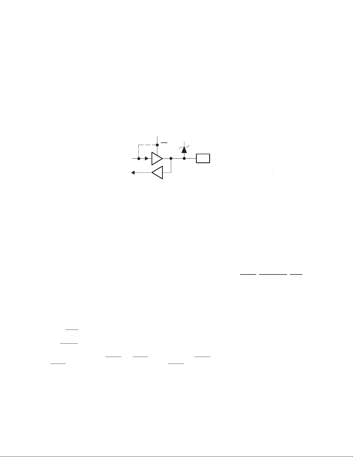
2. Remove the clamp voltage.
3. Remove the 3.3-V power from V
CC
.
NOTE: The clamp voltage can be ramped up or ramped down along with the 3.3-V power. The
voltage difference between V
and the clamp voltage must remain within 3.6 V.
CC
3.2 I/O Characteristics
Figure 3−2 shows a 3-state bidirectional buffer. Section 7.2, Recommended Operating Conditions, provides the
electrical characteristics of the inputs and outputs.
NOTE: The controller meets the ac specifications of the PC Card Standard and PCI Local Bus
Specification.
V
Tied for Open Drain
OE
CCP
Pad
Figure 3−2. 3-State Bidirectional Buffer
NOTE: Unused terminals (input or I/O) must be held high or low to prevent them from floating.
3.3 Clamping Voltages
The clamping voltages are set to match whatever external environment the controller is interfaced with, 3.3 V or 5 V.
The I/O sites can be pulled through a clamping diode to a voltage rail that protects the core from external signals.
The core power supply is always 3.3 V and is independent of the clamping voltages. For example, PCI signaling can
be either 3.3 V or 5 V, and the controller must reliably accommodate both voltage levels. This is accomplished by
using a 3.3-V I/O buffer that is 5-V tolerant, with the applicable clamping voltage applied. If a system designer desires
a 5-V PCI bus, then V
can be connected to a 5-V power supply.
CCP
The controller requires three separate clamping voltages because it supports a wide range of features. The three
voltages are listed and defined in Section 7.2, Recommended Operating Conditions. GRST
, SUSPEND, PME, and
CSTSCHG are not clamped to any of them.
3.4 Peripheral Component Interconnect (PCI) Interface
The controller is fully compliant with the PCI Local Bus Specification. The controller provides all required signals for
PCI master or slave operation, and may operate in either a 5-V or 3.3-V signaling environment by connecting the V
terminal to the desired voltage level. In addition to the mandatory PCI signals, the controller provides the optional
interrupt signal INTA
.
3.4.1 PCI GRST Signal
During the power-up sequence, GRST and PRST must be asserted. GRST can only be deasserted 100 µs after PCLK
is stable. PRST
can be deasserted at the same time as GRST or any time thereafter.
CCP
3−2

3.4.2 PCI Bus Lock (LOCK)
The bus-locking protocol defined in the PCI Local Bus Specification is not highly recommended, but is provided on
the controller as an additional compatibility feature. The PCI LOCK
setting the appropriate values in bits 19−16 of the multifunction routing register. See Section 4.30, Multifunction
Routing Register,
for details. Note that the use of LOCK is only supported by PCI-to-CardBus bridges in the
downstream direction (away from the processor).
signal can be routed to the MFUNC4 terminal by
PCI LOCK
indicates an atomic operation that may require multiple transactions to complete. When LOCK is asserted,
nonexclusive transactions can proceed to an address that is not currently locked. A grant to start a transaction on
the PCI bus does not guarantee control of LOCK
for different initiators to use the PCI bus while a single master retains ownership of LOCK
signal for this protocol is CBLOCK
to avoid confusion with the bus clock.
; control of LOCK is obtained under its own protocol. It is possible
. Note that the CardBus
An agent may need to do an exclusive operation because a critical access to memory might be broken into several
transactions, but the master wants exclusive rights to a region of memory. The granularity of the lock is defined by
PCI to be 16 bytes, aligned. The LOCK
protocol defined by the PCI Local Bus Specification allows a resource lock
without interfering with nonexclusive real-time data transfer, such as video.
The PCI bus arbiter may be designed to support only complete bus locks using the LOCK
the arbiter does not grant the bus to any other agent (other than the LOCK
master) while LOCK is asserted. A
protocol. In this scenario,
complete bus lock may have a significant impact on the performance of the video. The arbiter that supports complete
bus lock must grant the bus to the cache to perform a writeback due to a snoop to a modified line when a locked
operation is in progress.
The controller supports all LOCK
protocol associated with PCI-to-PCI bridges, as also defined for PCI-to-CardBus
bridges. This includes disabling write posting while a locked operation is in progress, which can solve a potential
deadlock when using devices such as PCI-to-PCI bridges. The potential deadlock can occur if a CardBus target
supports delayed transactions and blocks access to the target until it completes a delayed read. This target
characteristic is prohibited by the PCI Local Bus Specification, and the issue is resolved by the PCI master using
LOCK
.
3.4.3 Loading Subsystem Identification
The subsystem vendor ID register (PCI offset 40h, see Section 4.26) and subsystem ID register (PCI offset 42h, see
Section 4.27) make up a doubleword of PCI configuration space for function 0. This doubleword register is used for
system and option card (mobile dock) identification purposes and is required by some operating systems.
Implementation of this unique identifier register is a PC 99/PC 2001 requirement.
The controller offers two mechanisms to load a read-only value into the subsystem registers. The first mechanism
relies upon the system BIOS providing the subsystem ID value. The default access mode to the subsystem registers
is read-only, but can be made read/write by clearing bit 5 (SUBSYSR W) in the system control register (PCI of fset 80h,
see Section 4.29). Once this bit is cleared, the BIOS can write a subsystem identification value into the registers at
PCI offset 40h. The BIOS must set the SUBSYSRW bit such that the subsystem vendor ID register and subsystem
ID register is limited to read-only access. This approach saves the added cost of implementing the serial electrically
erasable programmable ROM (EEPROM).
In some conditions, such as in a docking environment, the subsystem vendor ID register and subsystem ID register
must be loaded with a unique identifier via a serial EEPROM. The controller loads the data from the serial EEPROM
after a reset of the primary bus. Note that the SUSPEND
serial-bus state machine (see Section 3.8.5, Suspend Mode, for details on using SUSPEND
input gates the PCI reset from the entire core, including the
).
The controller provides a two-line serial-bus host controller that can interface to a serial EEPROM. See Section 3.6,
Serial-Bus Interface,
for details on the two-wire serial-bus controller and applications.
3−3

3.5 PC Card Applications
This section describes the PC Card interfaces of the controller.
• Card insertion/removal and recognition
• Zoomed video support
• Speaker and audio applications
• LED socket activity indicators
• CardBus socket registers
3.5.1 PC Card Insertion/Removal and Recognition
The PC Card Standard (release 7.2) addresses the card-detection and recognition process through an interrogation
procedure that the socket must initiate on card insertion into a cold, nonpowered socket. Through this interrogation,
card voltage requirements and interface (16-bit versus CardBus) are determined.
The scheme uses the card-detect and voltage-sense signals. The configuration of these four terminals identifies the
card type and voltage requirements of the PC Card interface. The encoding scheme is defined in the PC Card
Standard (release 7.2) and in Table 3−1.
Table 3−1. PC Card Card-Detect and Voltage-Sense Connections
CD2//CCD2 CD1//CCD1 VS2//CVS2 VS1//CVS1 KEY INTERFACE VOLTAGE
Ground Ground Open Open 5 V 16-bit PC Card 5 V
Ground Ground Open Ground 5 V 16-bit PC Card 5 V and 3.3 V
Ground Ground Ground Ground 5 V 16-bit PC Card 5 V, 3.3 V, and X.X V
Ground Ground Open Ground LV 16-bit PC Card 3.3 V
Ground Connect to CVS1 Open Connect to CCD1 LV CardBus PC Card 3.3 V
Ground Ground Ground Ground LV 16-bit PC Card 3.3 V and X.X V
Connect to CVS2 Ground Connect to CCD2 Ground LV CardBus PC Card 3.3 V and X.X V
Connect to CVS1 Ground Ground Connect to CCD2 LV CardBus PC Card 3.3 V, X.X V, and Y.Y V
Ground Ground Ground Open LV 16-bit PC Card X.X V
Connect to CVS2 Ground Connect to CCD2 Open LV CardBus PC Card X.X V
Ground Connect to CVS2 Connect to CCD1 Open LV CardBus PC Card X.X V and Y.Y V
Connect to CVS1 Ground Open Connect to CCD2 LV CardBus PC Card Y.Y V
Ground Connect to CVS1 Ground Connect to CCD1 Reserved
Ground Connect to CVS2 Connect to CCD1 Ground Reserved
3.5.2 Parallel Power-Switch Interface (TPS2211A)
The controller provides a parallel interface for control of the PC Card power switch. The VCCD and VPPD terminals
are used with the TI TPS2211A single-slot PC Card power-switch interface to provide power-switch support.
Figure 3−3 illustrates a typical application, where the controller represents the PC Card controller.
3−4

Power Supply
12 V
5 V
3.3 V
12V
5V
3.3V
TPS2211A
Supervisor
PCI1510
(PC Card
Controller)
SHDN
SHDN
VCCD0
VCCD1
VPPD0
VPPD1
AVPP
AVCC
V
V
V
V
PP1
PP2
CC
CC
PC Card
Figure 3−3. TPS2211A Typical Application
3.5.3 Zoomed Video Support
The controller allows for the implementation of zoomed video (ZV) for PC Cards. Zoomed video is supported by
setting bit 6 (ZVENABLE) in the card control register (PCI offset 91h, see Section 4.32). Setting this bit puts 16-bit
PC Card address lines A25−A4 of the PC Card interface in the high-impedance state. These lines can then transfer
video and audio data directly to the appropriate controller. Card address lines A3−A0 can still access PC Card CIS
registers for PC Card configuration. Figure 3−4 illustrates a ZV implementation.
CRT
Speakers
Motherboard
PCI Bus
VGA
Controller
Zoomed Video
Port
PCI1510
Audio
Codec
19 4
PCM
Audio
Input
PC Card
19
PC Card
Interface
Video
Audio
4
Figure 3−4. Zoomed Video Implementation Using the PCI1510 Controller
Not shown in Figure 3−4 is the multiplexing scheme used to route a socket ZV source to the graphics controller. The
controller provides ZVSTAT and ZVSEL0
signals on the multifunction terminals to switch external bus drivers.
Figure 3−5 shows an implementation for switching between two ZV streams using external logic.
3−5

PCI1510
ZVSTAT
ZVSEL0
Figure 3−5. Zoomed Video Switching Application
Figure 3−5 illustrates an implementation using standard three-state bus drivers with active-low output enables.
ZVSEL0
is an active-low output indicating that the socket ZV mode is enabled.
3.5.4 Standardized Zoomed-Video Register Model
The standardized zoomed-video register model is defined for the purpose of standardizing the ZV port control for PC
Card controllers across the industry. The following list summarizes the standardized zoomed-video register model
changes to the existing PC Card register set.
• Socket present state register (CardBus socket address + 08h, see Section 6.3)
Bit 27 (ZVSUPPORT) has been added. The platform BIOS can set this bit via the socket force event register
(CardBus socket address + 0Ch, see Section 6.4) to define whether zoomed video is supported on the
socket by the platform.
• Socket force event register (CardBus socket address + 0Ch, see Section 6.4)
Bit 27 (FZVSUPPORT) has been added. The platform BIOS can use this bit to set the ZVSUPPORT bit in
the socket present state register (CardBus socket address + 08h, see Section 6.3) to define whether
zoomed video is supported on the socket by the platform.
• Socket control register (CardBus socket address +10h, see Section 6.5)
Bit 11 (ZV_ACTIVITY) has been added. This bit is set when zoomed video is enabled for the PC Card socket.
Bit 10 (STDZVREG) has been added. This bit defines whether the PC Card controller supports the
standardized zoomed-video register model.
Bit 9 (ZVEN) is provided for software to enable or disable zoomed video.
If the STDZVEN bit (bit 0) in the diagnostic register (PCI offset 93h, see Section 4.34) is 1b, then the standardized
zoomed video register model is disabled. For backward compatibility, even if the STDZVEN bit is 0b (enabled), the
controller allows software to access zoomed video through the legacy address in the card control register (PCI offset
91h, see Section 4.32), or through the new register model in the socket control register (CardBus socket address +
10h, see Section 6.5).
3.5.4.1 Zoomed-Video Card Insertion and Configuration Procedure
1. A zoomed-video PC Card is inserted into an empty slot.
2. The card is detected and interrogated appropriately.
3−6

There are two types of PC Card controllers to consider.
SIGNAL NAME
SIGNAL NAME
• Legacy controller not using the standardized ZV register model
Software reads bit 10 (STDZVREG) of the socket control register (CardBus socket address + 10h) to
determine if the standardized zoomed-video register model is supported. If the bit returns 0b, then software
must use legacy code to enable zoomed video.
• Newer controller that uses the standardized ZV register model
Software reads bit 10 (STDZVREG) of the socket control register (CardBus socket address + 10h) to
determine if the standardized zoomed-video register model is supported. If the bit returns 1b, then software
can use the process/register model detailed in Table 3−2 to enable zoomed video.
Table 3−2. Zoomed-Video Card Interrogation
ZVSUPPORT ZV_ACTIVITY ACTION
1 0 Set ZVEN to enable zoomed video.
1 1
0 X
Display a user message such as, The zoomed video protocol required by this PC Card application is al-
ready in use by another card.
Display a user message such as, This platform does not support the zoomed-video protocol required by
this PC Card application.
3.5.5 Internal Ring Oscillator
The internal ring oscillator provides an internal clock source for the controller so that neither the PCI clock nor an
external clock is required in order for the controller to power down a socket or interrogate a PC Card. This internal
oscillator can be enabled by setting bit 27 (P2CCLK) of the system control register (PCI offset 80h, see Section 4.29)
to 1b. This function is enabled by default.
3.5.6 Integrated Pullup Resistors
The PC Card Standard (release 7.2) requires pullup resistors on various terminals to support both CardBus and 16-bit
card configurations. Unlike the PCI12XX, PCI1450, and PCI4450 controllers which required external pullup resistors,
the PCI1510 controller has integrated all of these pullup resistors. The I/O buffer on the BVD1(STSCHG
terminal has the capability to switch either pullup or pulldown. The pullup resistor is turned on when a 16-bit PC Card
is inserted, and the pulldown resistor is turned on when a CardBus PC Card is inserted. This prevents unexpected
CSTSCHG signal assertion. The integrated pullup resistors are listed in Table 3−3.
Table 3−3. Integrated Pullup Resistors
TERMINAL NUMBER
PGE GGU GVF
A14/CPERR 102 D12 F15 CD2/CCD2 138 B05 C09
A15/CIRDY 110 C10 F13 INPACK/CREQ 122 B08 B12
A19/CBLOCK 101 A13 E18 READY/CINT 131 A06 C10
A20/CSTOP 103 E10 E17 RESET/CRST 119 D08 B13
A21/CDEVSEL 106 D11 A16 VS1/CVS1 130 B02 B10
A22/CTRDY 108 C12 E14 VS2/CVS2 117 A09 F12
BVD1(STSCHG)/CSTSCHG 135 C06 A09 WAIT/CSERR 133 B06 E10
BVD2(SPKR)/CAUDIO 134 D06 F10 WP(IOIS16)/CCLKRUN 136 A05 B09
CD1/CCD1 75 L13 L17
TERMINAL NUMBER
PGE GGU GVF
)//CSTSCHG
3−7

3.5.7 SPKROUT and CAUDPWM Usage
SPKROUT carries the digital audio signal from the PC Card to the system. When a 16-bit PC Card is configured for
I/O mode, the BVD2 terminal becomes SPKR
is referred to as CAUDIO. SPKR
passes a TTL-level digital audio signal to the controller. The CardBus CAUDIO signal
also can pass a single-amplitude binary waveform. The binary audio signal from the PC Card socket is used in the
controller to produce SPKROUT. This output is enabled by bit 1 (SPKROUTEN) in the card control register (PCI offset
91h, see Section 4.32).
Older controllers support CAUDIO in binary or PWM mode but use the same terminal (SPKROUT). Some audio chips
may not support both modes on one terminal and may have a separate terminal for binary and PWM. The
implementation includes a signal for PWM, CAUDPWM, which can be routed to an MFUNC terminal. Bit 2
(AUD2MUX), located in the card control register, is programmed to route a CardBus CAUDIO PWM terminal to
CAUDPWM. See Section 4.30, Multifunction Routing Register, for details on configuring the MFUNC terminals.
Figure 3−6 provides an illustration of a sample application using SPKROUT and CAUDPWM.
System
Core Logic
SPKROUT
PCI1510
CAUDPWM
. This terminal is also used in CardBus binary audio applications, and
BINARY_SPKR
Speaker
Subsystem
PWM_SPKR
Figure 3−6. Sample Application of SPKROUT and CAUDPWM
3.5.8 LED Socket Activity Indicators
The socket activity LED is provided to indicate when a PC Card is being accessed. The LED_SKT signal can be routed
to the multifunction terminals. When configured for LED output, this terminal outputs an active high signal to indicate
socket activity. See Section 4.30, Multifunction Routing Register,
terminals.
The active-high LED signal is driven for 64-ms. When the LED is not being driven high, it is driven to a low state. Either
of the two circuits shown in Figure 3−7 can be implemented to provide LED signaling, and the board designer must
implement the circuit that best fits the application.
The LED activity signal is valid when a card is inserted, powered, and not in reset. For PC Card-16, the LED activity
signal is pulsed when READY/IREQ
or CREQ
are active.
is low. For CardBus cards, the LED activity signal is pulsed if CFRAME, IRDY,
for details on configuring the multifunction
3−8

Current Limiting
R ≈ 500 Ω
PCI1510
PCI1510
Application-
Specific Delay
Current Limiting
R ≈ 500 Ω
LED
LED
Figure 3−7. Two Sample LED Circuits
As indicated, the LED signal is driven for a period of 64 ms by a counter circuit. To avoid the possibility of the LED
appearing to be stuck when the PCI clock is stopped, the LED signaling is cut off when the SUSPEND
signal is
asserted, when the PCI clock is to be stopped during the clock run protocol, or when in the D2 or D1 power state.
If any additional socket activity occurs during this counter cycle, then the counter is reset and the LED signal remains
driven. If socket activity is frequent (at least once every 64 ms), then the LED signals remain driven.
3.5.9 CardBus Socket Registers
The controller contains all registers for compatibility with the PC Card Standard. These registers exist as the CardBus
socket registers and are listed in Table 3−4.
Table 3−4. CardBus Socket Registers
REGISTER NAME OFFSET
Socket event 00h
Socket mask 04h
Socket present state 08h
Socket force event 0Ch
Socket control 10h
Reserved 14h−1Ch
Socket power management 20h
3.6 Serial-Bus Interface
The controller provides a serial-bus interface to load subsystem identification information and selected register
defaults from a serial EEPROM, and to provide a PC Card power-switch interface alternative. The serial-bus interface
is compatible with various I
3.6.1 Serial-Bus Interface Implementation
To enable the serial interface, a pullup resistor must be implemented on the VCCD0 and VCCD1 terminals and the
appropriate pullup resistors must be implemented on the SDA and SCL signals, that is, the MFUNC1 and MFUNC4
terminals. When the interface is detected, bit 3 (SBDETECT) in the serial bus control and status register (PCI offset
B3h, see Section 4.48) is set. The SBDETECT bit is cleared by a writeback of 1b.
The controller implements a two-pin serial interface with one clock signal (SCL) and one data signal (SDA). When
pullup resistors are provided on the VCCD0
and the SDA signal is mapped to the MFUNC1 terminal. The controller drives SCL at nearly 100 kHz during data
2
C and SMBus components.
and VCCD1 terminals, the SCL signal is mapped to the MFUNC4 terminal
3−9

transfers, which is the maximum specified frequency for standard-mode I2C. The serial EEPROM must be located
at address A0h. Figure 3−8 illustrates an example application implementing the two-wire serial bus.
V
CC
Serial
EEPROM
A2
A1
A0
SCL
SDA
PCI1510
VCCD0
VCCD1
MFUNC4
MFUNC1
5 V
Figure 3−8. Serial EEPROM Application
Some serial device applications may include PC Card power switches, ZV source switches, card ejectors, or other
devices that may enhance the user’s PC Card experience. The serial EEPROM device and PC Card power switches
are discussed in the sections that follow.
3.6.2 Serial-Bus Interface Protocol
The SCL and SDA signals are bidirectional, open-drain signals and require pullup resistors as shown in Figure 3−8.
The controller, which supports up to 100-Kb/s data-transfer rate, is compatible with standard mode I
addressing.
All data transfers are initiated by the serial bus master. The beginning of a data transfer is indicated by a start
condition, which is signaled when the SDA line transitions to low state while SCL is in the high state, as illustrated
in Figure 3−9. The end of a requested data transfer is indicated by a stop condition, which is signaled by a low-to-high
transition of SDA while SCL is in the high state, as shown in Figure 3−9. Data on SDA must remain stable during the
high state of the SCL signal, as changes on the SDA signal during the high state of SCL are interpreted as control
signals, that is, a start or a stop condition.
2
C using 7-bit
SDA
SCL
Start
Condition
Stop
Condition
Change of
Data Allowed
Data Line Stable,
Data Valid
Figure 3−9. Serial-Bus Start/Stop Conditions and Bit Transfers
Data is transferred serially in 8-bit bytes. The number of bytes that may be transmitted during a data transfer is
unlimited; however, each byte must be completed with an acknowledge bit. An acknowledge (ACK) is indicated by
the receiver pulling the SDA signal low, so that it remains low during the high state of the SCL signal. Figure 3−10
illustrates the acknowledge protocol.
3−10

SCL From
Master
SDA Output
By Transmitter
SDA Output
By Receiver
123 789
Figure 3−10. Serial-Bus Protocol Acknowledge
The controller is a serial bus master; all other devices connected to the serial bus external to the controller are slave
devices. As the bus master, the controller drives the SCL clock at nearly 100 kHz during bus cycles and places SCL
in a high-impedance state (zero frequency) during idle states.
Typically, the controller masters byte reads and byte writes under software control. Doubleword reads are performed
by the serial EEPROM initialization circuitry upon a PCI reset and may not be generated under software control. See
Section 3.6.3, Serial-Bus EEPROM Application, for details on how the controller automatically loads the subsystem
identification and other register defaults through a serial-bus EEPROM.
Figure 3−11 illustrates a byte write. The controller issues a start condition and sends the 7-bit slave device address
and the command bit zero. A 0b in the R/W
command bit indicates that the data transfer is a write. The slave device
acknowledges if it recognizes the address. If no acknowledgment is received by the controller, then an appropriate
status bit is set in the serial-bus control and status register (PCI offset B3h, see Section 4.48). The word address byte
is then sent by the controller, and another slave acknowledgment is expected. Then the controller delivers the data
byte MSB first and expects a final acknowledgment before issuing the stop condition.
Slave Address Word Address
Sb6 b4b5 b3 b2 b1 b0 0 b7 b6 b5 b4 b3 b2 b1 b0AA
R/W
S/P = Start/Stop ConditionA = Slave Acknowledgement
b7 b6 b4b5 b3 b2 b1 b0 A P
Data Byte
Figure 3−11. Serial-Bus Protocol − Byte Write
Figure 3−12 illustrates a byte read. The read protocol is very similar to the write protocol, except the R/W
command
bit must be set to 1b to indicate a read-data transfer. In addition, the master must acknowledge reception of the read
bytes from the slave transmitter. The slave transmitter drives the SDA signal during read data transfers. The SCL
signal remains driven by the master.
Slave Address Word Address
Sb6 b4b5 b3 b2 b1 b0 0 b7 b6 b5 b4 b3 b2 b1 b0AA
Start
A = Slave Acknowledgement
R/W
Sb6 b4b5 b3 b2 b1 b0 1 A
Restart R/W
b7 b6 b4b5 b3 b2 b1 b0 M P
S/P = Start/Stop ConditionM = Master Acknowledgement
Slave Address
Data Byte
Stop
Figure 3−12. Serial-Bus Protocol − Byte Read
Figure 3−13 illustrates EEPROM interface doubleword data collection protocol.
3−11

Slave Address Word Address
Slave Address
S1 10 0 0 0 0 0 b7b6b5b4b3b2b1b0AA
Start
Data Byte 3 M
R/W
Data Byte 2 Data Byte 1 Data Byte 0 M PMM
M = Master Acknowledgement
S1 10 00001A
Restart
S/P = Start/Stop ConditionA = Slave Acknowledgement
R/W
Figure 3−13. EEPROM Interface Doubleword Data Collection
3.6.3 Serial-Bus EEPROM Application
When the PCI bus is reset and the serial-bus interface is detected, the controller attempts to read the subsystem
identification and other register defaults from a serial EEPROM. The registers and corresponding bits that can be
loaded with defaults through the EEPROM are provided in Table 3−5.
Table 3−5. Register- and Bit-Loading Map
EEPROM OFFSET REGISTER OFFSET REGISTER BITS LOADED FROM EEPROM
00h Flag 01h: Load / FFh: do not load
01h PCI 04h Command register, bit 8, 6−5, 2−0
02h PCI 40h Subsystem vendor ID bits 7−0 ← bits 7−0
03h PCI 40h Subsystem vendor ID bits 15−8 ← bits 7−0
04h PCI 42h Subsystem ID bits 7−0 ← bits 7−0
05h PCI 42h Subsystem ID bits 15−8 ← bits 7−0
06h PCI 44h PC Card 16-bit I/F LBAR bits 7−1 ← bits 7−1
07h PCI 44h PC Card 16-bit I/F LBAR bits 15−8 ← bits 7−0
08h PCI 44h PC Card 16-bit I/F LBAR bits 23−16 ← bits 7−0
09h PCI 44h PC Card 16-bit I/F LBAR bits 31−24 ← bits 7−0
0Ah PCI 80h System control bits 7−0 ← bits 7−0
0Bh PCI 80h System control bits 15−8 ← bits 7−0
0Ch PCI 80h System control bits 23−16 ← bits 7−0
0Dh PCI 80h System control bits 31−24 ← bits 7−0
0Eh PCI 8Ch Multifunction routing bits 7−0 ← bits 7−0
0Fh PCI 8Ch Multifunction routing bits 15−8 ← bits 7−0
10h PCI 8Ch Multifunction routing bits 23−16 ← bits 7−0
11h PCI 8Ch Multifunction routing bits 27−24 ← bits 3−0
12h PCI 90h Retry status bits 7, 6 ← bits 7, 6
13h PCI 91h Card control bit 7 ← bit 7
14h PCI 92h Device control bits 6, 3−0 ← bits 6, 3−0
15h PCI 93h Diagnostic bits 7, 4–0 ← bits 7, 4−0
16h PCI A2h Power management capabilities bit 15 ← bit 7
17h ExCA 00h ExCA identification and revision bits 7–0 ← bits 7−0
18h CB Socket + 0Ch Socket force event, bit 27 ← bit 3
Note: bits loaded per following:
bit 8 ← bit 7
bit 6 ← bit 6
bit 5 ← bit 5
bit 2 ← bit 2
bit 1 ← bit 1
bit 0 ← bit 0
3−12

This format must be followed for the controller to load initializations from a serial EEPROM. All bit fields must be
considered when programming the EEPROM.
The serial EEPROM is addressed at slave address 1010 000b by the controller. All hardware address bits for the
EEPROM should be tied to the appropriate level to achieve this address. The serial EEPROM chip in the sample
application circuit (Figure 3−8) assumes the 1010b high-address nibble. The lower three address bits are terminal
inputs to the chip, and the sample application shows these terminal inputs tied to GND.
3.6.4 Accessing Serial-Bus Devices Through Software
The controller provides a programming mechanism to control serial bus devices through software. The programming
is accomplished through a doubleword of PCI configuration space at offset B0h. Table 3−6 lists the registers used
to program a serial-bus device through software.
Table 3−6. PCI1510 Registers Used to Program Serial-Bus Devices
PCI OFFSET REGISTER NAME DESCRIPTION
B0h Serial-bus data Contains the data byte to send on write commands or the received data byte on read commands.
B1h Serial-bus index
B2h
B3h
Serial-bus slave
address
Serial-bus control
and status
The content of this register is sent as the word address on byte writes or reads. This register is not used
in the quick command protocol.
Write transactions to this register initiate a serial-bus transaction. The slave device address and the
R/W
command selector are programmed through this register.
Read data valid, general busy, and general error status are communicated through this register. In
addition, the protocol-select bit is programmed through this register.
3.7 Programmable Interrupt Subsystem
Interrupts provide a way for I/O devices to let the microprocessor know that they require servicing. The dynamic
nature of PC Cards and the abundance of PC Card I/O applications require substantial interrupt support from the
controller. The controller provides several interrupt signaling schemes to accommodate the needs of a variety of
platforms. The different mechanisms for dealing with interrupts in this device are based on various specifications and
industry standards. The ExCA register set provides interrupt control for some 16-bit PC Card functions, and the
CardBus socket register set provides interrupt control for the CardBus PC Card functions. The controller is, therefore,
backward compatible with existing interrupt control register definitions, and new registers have been defined where
required.
The controller detects PC Card interrupts and events at the PC Card interface and notifies the host controller using
one of several interrupt signaling protocols. T o simplify the discussion of interrupts in the controller, PC Card interrupts
are classified either as card status change (CSC) or as functional interrupts.
The method by which any type of interrupt is communicated to the host interrupt controller varies from system to
system. The controller offers system designers the choice of using parallel PCI interrupt signaling, parallel ISA-type
IRQ interrupt signaling, or the IRQSER serialized ISA and/or PCI interrupt protocol. It is possible to use the parallel
PCI interrupts in combination with either parallel IRQs or serialized IRQs, as detailed in the sections that follow. All
interrupt signaling is provided through the seven multifunction terminals, MFUNC0−MFUNC6.
3.7.1 PC Card Functional and Card Status Change Interrupts
PC Card functional interrupts are defined as requests from a PC Card application for interrupt service and are
indicated by asserting specially-defined signals on the PC Card interface. Functional interrupts are generated by
16-bit I/O PC Cards and by CardBus PC Cards.
Card status change (CSC)-type interrupts are defined as events at the PC Card interface that are detected by the
controller and may warrant notification of host card and socket services software for service. CSC events include both
card insertion and removal from the PC Card socket, as well as transitions of certain PC Card signals.
3−13
Table 3−7 summarizes the sources of PC Card interrupts and the type of card associated with them. CSC and
CardBus
Battery conditions
Battery conditions
memory
All PC Cards
All PC Cards
functional interrupt sources are dependent on the type of card inserted in the PC Card socket. The three types of cards
that can be inserted into any PC Card socket are:
• 16-bit memory card
• 16-bit I/O card
• CardBus cards
Table 3−7. Interrupt Mask and Flag Registers
CARD TYPE EVENT MASK FLAG
16-bit memory
16-bit I/O
All 16-bit PC
Cards
Battery conditions (BVD1, BVD2) ExCA offset 05h/45h/805h bits 1 and 0 ExCA offset 04h/44h/804h bits 1 and 0
Wait states (READY) ExCA offset 05h/45h/805h bit 2 ExCA offset 04h/44h/804h bit 2
Change in card status (STSCHG) ExCA offset 05h/45h/805h bit 0 ExCA offset 04h/44h/804h bit 0
Interrupt request (IREQ) Always enabled PCI configuration offset 91h bit 0
Power cycle complete ExCA offset 05h/45h/805h bit 3 ExCA offset 04h/44h/804h bit 3
Change in card status (CSTSCHG) Socket mask bit 0 Socket event bit 0
Interrupt request (CINT) Always enabled PCI configuration offset 91h bit 0
Power cycle complete Socket mask bit 3 Socket event bit 3
Card insertion or removal Socket mask bits 2 and 1 Socket event bits 2 and 1
Functional interrupt events are valid only for 16-bit I/O and CardBus cards; that is, the functional interrupts are not
valid for 16-bit memory cards. Furthermore, card insertion and removal-type CSC interrupts are independent of the
card type.
Table 3−8. PC Card Interrupt Events and Description
CARD TYPE EVENT TYPE SIGNAL DESCRIPTION
A transition on BVD1 indicates a change in the
PC Card battery conditions.
A transition on BVD2 indicates a change in the
PC Card battery conditions.
A transition on READY indicates a change in the
ability of the memory PC Card to accept or provide
data.
The assertion of STSCHG indicates a status change
on the PC Card.
The assertion of IREQ indicates an interrupt request
from the PC Card.
The assertion of CSTSCHG indicates a status
change on the PC Card.
The assertion of CINT indicates an interrupt request
from the PC Card.
A transition on either CD1//CCD1 or CD2//CCD2
indicates an insertion or removal of a 16-bit or
CardBus PC Card.
An interrupt is generated when a PC Card power-up
cycle has completed.
16-bit
16-bit I/O
CardBus
(BVD1, BVD2)
Wait states
(READY)
Change in card
status (STSCHG
Interrupt request
(IREQ
)
Change in card
status (CSTSCHG)
Interrupt request
(CINT
)
Card insertion
or removal
Power cycle
complete
BVD1(STSCHG)//CSTSCHG
CSC
BVD2(SPKR)//CAUDIO
CSC READY(IREQ)//CINT
CSC BVD1(STSCHG)//CSTSCHG
)
Functional READY(IREQ)//CINT
CSC BVD1(STSCHG)//CSTSCHG
Functional READY(IREQ)//CINT
CSC
CSC N/A
CD1//CCD1,
CD2
//CCD2
The naming convention for PC Card signals describes the function for 16-bit memory, I/O cards, and CardBus. For
example, READY(IREQ
)//CINT includes READY for 16-bit memory cards, IREQ for 16-bit I/O cards, and CINT for
CardBus cards. The 16-bit memory card signal name is first, with the I/O card signal name second, enclosed in
parentheses. The CardBus signal name follows after a double slash (//).
3−14

The PC Card Standard describes the power-up sequence that must be followed by the controller when an insertion
event occurs and the host requests that the socket V
and VPP be powered. Upon completion of this power-up
CC
sequence, the interrupt scheme can be used to notify the host system (see Table 3−8), denoted by the power cycle
complete event. This interrupt source is considered an internal event, because it depends on the completion of
applying power to the socket rather than on a signal change at the PC Card interface.
3.7.2 Interrupt Masks and Flags
Host software may individually mask (or disable) most of the potential interrupt sources listed in Table 3−8 by setting
the appropriate bits in the controller. By individually masking the interrupt sources listed, software can control those
events that cause an interrupt. Host software has some control over the system interrupt the controller asserts by
programming the appropriate routing registers. The controller allows host software to route PC Card CSC and PC
Card functional interrupts to separate system interrupts. Interrupt routing somewhat specific to the interrupt signaling
method used is discussed in more detail in the following sections.
When an interrupt is signaled by the controller, the interrupt service routine must determine which of the events listed
in Table 3−7 caused the interrupt. Internal registers in the controller provide flags that report the source of an interrupt.
By reading these status bits, the interrupt service routine can determine the action to be taken.
Table 3−7 details the registers and bits associated with masking and reporting potential interrupts. All interrupts can
be masked except the functional PC Card interrupts, and an interrupt status flag is available for all types of interrupts.
Notice that there is not a mask bit to stop the controller from passing PC Card functional interrupts through to the
appropriate interrupt scheme. These interrupts are not valid until the card is properly powered, and there should never
be a card interrupt that does not require service after proper initialization.
Table 3−7 lists the various methods of clearing the interrupt flag bits. The flag bits in the ExCA registers (16-bit PC
Card-related interrupt flags) can be cleared using two different methods. One method is an explicit write of 1b to the
flag bit to clear and the other is by reading the flag bit register. The selection of flag bit clearing methods is made by
bit 2 (IFCMODE) in the ExCA global control register (ExCA offset 1Eh/5Eh/81Eh, see Section 5.20), and defaults to
the flag-cleared-on-read method.
The CardBus-related interrupt flags can be cleared by an explicit write of 1b to the interrupt flag in the socket event
register (see Section 6.1). Although some of the functionality is shared between the CardBus registers and the ExCA
registers, software should not program the chip through both register sets when a CardBus card is functioning.
3.7.3 Using Parallel IRQ Interrupts
The seven multifunction terminals, MFUNC6−MFUNC0, implemented in the controller can be routed to obtain a
subset of the ISA IRQs. The IRQ choices provide ultimate flexibility in PC Card host interruptions. To use the parallel
ISA-type IRQ interrupt signaling, software must program the device control register (PCI offset 92h, see
Section 4.33), to select the parallel IRQ signaling scheme. See Section 4.30, Multifunction Routing Register, for
details on configuring the multifunction terminals.
A system using parallel IRQs requires (at a minimum) one PCI terminal, INTA
is dictated by certain card and socket-services software. The INT A
for INTA
signaling. This leaves (at a maximum) six different IRQs to support legacy 16-bit PC Card functions.
requirement calls for routing the MFUNC0 terminal
As an example, suppose the six IRQs used by legacy PC Card applications are IRQ3, IRQ4, IRQ5, IRQ10, IRQ11,
and IRQ15. The multifunction routing register must be programmed to a value of 0FBA 5432h. This value routes the
MFUNC0 terminal to INTA
that INTA
must also be routed to the programmable interrupt controller (PIC), or to some circuitry that provides parallel
signaling and routes the remaining terminals as illustrated in Figure 3−14. Not shown is
PCI interrupts to the host.
, to signal CSC events. This requirement
3−15

PCI1510 PIC
MFUNC1
MFUNC2
MFUNC3
MFUNC4
MFUNC5
MFUNC6
IRQ3
IRQ4
IRQ5
IRQ10
IRQ11
IRQ15
Figure 3−14. IRQ Implementation
Power-on software is responsible for programming the multifunction routing register to reflect the IRQ configuration
of a system implementing the controller. See Section 4.30, Multifunction Routing Register,
for details on configuring
the multifunction terminals.
The parallel ISA-type IRQ signaling from the MFUNC6−MFUNC0 terminals is compatible with the input signal
requirements of the 8259 PIC. The parallel IRQ option is provided for system designs that require legacy ISA IRQs.
Design constraints may demand more MFUNC6−MFUNC0 IRQ terminals than the controller makes available.
3.7.4 Using Parallel PCI Interrupts
Parallel PCI interrupts are available when exclusively in parallel PCI interrupt/parallel ISA IRQ signaling mode, and
when only IRQs are serialized with the IRQSER protocol. Socket functional interrupts can be routed to INTA
.
3.7.5 Using Serialized IRQSER Interrupts
The serialized interrupt protocol implemented in the controller uses a single terminal to communicate all interrupt
status information to the host controller. The protocol defines a serial packet consisting of a start cycle, multiple
interrupt indication cycles, and a stop cycle. All data in the packet is synchronous with the PCI clock. The packet data
describes 16 parallel ISA IRQ signals and the optional 4 PCI interrupts INTA
the IRQSER protocol, refer to the document Serialized IRQ Support for PCI Systems.
, INTB, INTC, and INTD. For details on
3.7.6 SMI Support in the PCI1510 Controller
The controller provides a mechanism for interrupting the system when power changes have been made to the PC
Card socket interfaces. The interrupt mechanism is designed to fit into a system maintenance interrupt (SMI) scheme.
SMI interrupts are generated by the controller, when enabled, after a write cycle to either the socket control register
(CB offset 10h, see Section 6.5) of the CardBus register set, or the ExCA power control register (ExCA offset
02h/42h/802h, see Section 5.3) causes a power cycle change sequence to be sent on the power switch interface.
The SMI control is programmed through three bits in the system control register (PCI offset 80h, see Section 4.29).
These bits are SMIROUTE (bit 26), SMIST ATUS (bit 25), and SMIENB (bit 24). Table 3−9 describes the SMI control
bits function.
Table 3−9. SMI Control
BIT NAME FUNCTION
SMIROUTE This shared bit controls whether the SMI interrupts are sent as a CSC interrupt or as IRQ2.
SMISTAT This socket dependent bit is set when an SMI interrupt is pending. This status flag is cleared by writing back 1b.
SMIENB When set, SMI interrupt generation is enabled.
If CSC SMI interrupts are selected, then the SMI interrupt is sent as the CSC on a per-socket basis. The CSC interrupt
can be either level or edge mode, depending upon the CSCMODE bit in the ExCA global control register (ExCA offset
1Eh/5Eh/81Eh, see Section 5.20).
If IRQ2 is selected by SMIROUTE, then the IRQSER signaling protocol supports SMI signaling in the IRQ2 IRQ/Data
slot. In a parallel ISA IRQ system, the support for an active low IRQ2 is provided only if IRQ2 is routed to either
MFUNC3 or MFUNC6 through the multifunction routing register (PCI offset 8Ch, see Section 4.30).
3−16

3.8 Power Management Overview
In addition to the low-power CMOS technology process used for the controller, various features are designed into
the device to allow implementation of popular power-saving techniques. These features and techniques are
discussed in this section.
3.8.1 Integrated Low-Dropout Voltage Regulator (LDO-VR)
The controller requires 2.5-V core voltage. The core power can be supplied by the controller itself using the internal
LDO-VR. The core power can alternatively be supplied by an external power supply through the VR_PORT terminal.
Table 3−10 lists the requirements for both the internal core power supply and the external core power supply.
Table 3−10. Requirements for Internal/External 2.5-V Core Power Supply
SUPPLY V
Internal 3.3 V GND 2.5-V output Internal 2.5-V LDO-VR is enabled. A 1.0-µF bypass capacitor is required on the VR_PORT
External 3.3 V V
3.8.2 Clock Run Protocol
The PCI CLKRUN feature is the primary method of power management on the PCI interface of the controller.
CLKRUN
is not always available to the system designer, and alternate power-saving features are provided. For details on the
CLKRUN
The controller does not permit the central resource to stop the PCI clock under any of the following conditions:
The controller restarts the PCI clock using the CLKRUN
signaling is provided through the MFUNC6 terminal. Since some chip sets do not implement CLKRUN, this
protocol see the PCI Mobile Design Guide.
• Bit 1 (KEEPCLK) in the system control register (PCI offset 80h, see Section 4.29) is set.
• The 16-bit PC Card- resource manager is busy.
• The CardBus master state machine is busy. A cycle may be in progress on CardBus.
• The master is busy. There may be posted data from CardBus to PCI in the controller.
• Interrupts are pending.
• The CardBus CCLK for either socket has not been stopped by the CCLKRUN
• A 16-bit PC Card IREQ
• A CardBus CBWAKE (CSTSCHG) or 16-bit PC Card STSCHG
• A CardBus attempts to start the CCLK using CCLKRUN
• A CardBus card arbitrates for the CardBus bus using CREQ
VR_EN VR_PORT NOTE
CC
CC
2.5-V input Internal 2.5-V LDO-VR is disabled. An external 2.5-V power supply, of minimum 50-mA
or a CardBus CINT has been asserted by either card.
terminal for decoupling. This output is not for external use.
capacity, is required. A 0.1-µF bypass capacitor on the VR_PORT terminal is required.
manager.
protocol under any of the following conditions:
/RI event occurs in either socket.
.
.
3.8.3 CardBus PC Card Power Management
The controller implements its own card power-management engine that can turn off the CCLK to a socket when there
is no activity to the CardBus PC Card. The PCI clock-run protocol is followed on the CardBus CCLKRUN
interface
to control this clock management.
3.8.4 16-Bit PC Card Power Management
The COE bit (bit 7) of the ExCA power control register (ExCA offset 02h/42h/802h, see Section 5.3) and PWRDWN
bit (bit 0) of the ExCA global control register (ExCA offset 1Eh/5Eh/81Eh, see Section 5.20) bits are provided for 16-bit
PC Card power management. The COE bit places the card interface in a high-impedance state to save power. The
power savings when using this feature are minimal. The COE bit resets the PC Card when used, and the PWRDWN
bit does not. Furthermore, the PWRDWN bit is an automatic COE, that is, the PWRDWN performs the COE function
when there is no card activity.
NOTE: The 16-bit PC Card must implement the proper pullup resistors for the COE and
PWRDWN modes.
3−17

3.8.5 Suspend Mode
The SUSPEND signal, provided for backward compatibility, gates the PRST (PCI reset) signal and the GRST (global
reset) signal from the controller. Besides gating PRST
in order to minimize power consumption.
and GRST, SUSPEND also gates PCLK inside the controller
It should also be noted that asynchronous signals, such as card status change interrupts and RI_OUT
, can be passed
to the host system without a PCI clock. However, if card status change interrupts are routed over the serial interrupt
stream, then the PCI clock must be restarted in order to pass the interrupt, because neither the internal oscillator nor
an external clock is routed to the serial-interrupt state machine. Figure 3−15 is a signal diagram of the suspend
function.
RESET
GNT
SUSPEND
PCLK
External Terminals
Internal Signals
RESETIN
SUSPENDIN
PCLKIN
Figure 3−15. Signal Diagram of Suspend Function
3.8.6 Requirements for Suspend Mode
The suspend mode prevents the clearing of all register contents on the assertion of reset (PRST or GRST) which
would require the reconfiguration of the controller by software. Asserting the SUSPEND
of the controller in a high-impedance state and gates the PCLK signal internally to the controller unless a PCI
transaction is currently in process (GNT
when SUSPEND
is asserted, because the outputs are in a high-impedance state.
The GPIOs, MFUNC signals, and RI_OUT
is asserted). It is important that the PCI bus not be parked on the controller
signal are all active during SUSPEND, unless they are disabled in the
appropriate registers.
signal places the PCI outputs
3−18

3.8.7 Ring Indicate
The RI_OUT output is an important feature in power management, allowing a system to go into a suspended mode
and wake up on modem rings and other card events. TI-designed flexibility permits this signal to fit wide platform
requirements. RI_OUT
on the controller can be asserted under any of the following conditions:
• A 16-bit PC Card modem in a powered socket asserts RI
to indicate to the system the presence of an
incoming call.
• A powered down CardBus card asserts CSTSCHG (CBWAKE) requesting system and interface wake up.
• A powered CardBus card asserts CSTSCHG from the insertion/removal of cards or change in battery
voltage levels.
Figure 3−16 shows various enable bits for the RI_OUT
function; however, it does not show the masking of CSC
events. See Table 3−7 for a detailed description of CSC interrupt masks and flags.
RI_OUT Function
PC Card
Socket
Card
I/F
CSTSMASK
RINGEN
CDRESUME
RIENB
RI_OUT
Figure 3−16. RI_OUT Functional Diagram
from the 16-bit PC Card interface is masked by bit 7 (RINGEN) in the ExCA interrupt and general control register
RI
(ExCA offset 03h/43h/803h, see Section 5.4). This is only applicable when a 16-bit card is powered in the socket.
The CBWAKE signaling to RI_OUT
is enabled through the same mask as the CSC event for CSTSCHG. The mask
bit (bit 0, CSTSMASK) is programmed through the socket mask register (CB offset 04h, see Section 6.2) in the
CardBus socket registers.
RI_OUT
can be routed through any of three different pins, RI_OUT/PME, MFUNC2, or MFUNC4. The RI_OUT
function is enabled by setting RIENB in the card control register (PCI offset 91h, see Section 4.32). The PME function
is enabled by setting PMEEN in the power management control/status register (PCI offset A4h, see Section 4.38).
When RIMUX in the system control register (PCI offset 80h, see Section 4.29) is set to 0b, both the RI_OUT
and the PME
the RI_OUT
using both the RI_OUT
function are routed to the RI_OUT/PME terminal. If both functions are enabled and RIMUX is set to 0b,
/PME terminal becomes RI_OUT only and PME assertions will never be seen. Therefore, in a system
function and the PME function, RIMUX must be set to 1b and RI_OUT must be routed to either
function
MFUNC2 or MFUNC4.
3.8.8 PCI Power Management
The PCI Bus Power Management Interface Specification for PCI to CardBus Bridges establishes the infrastructure
required to let the operating system control the power of PCI functions. This is done by defining a standard PCI
interface and operations to manage the power of PCI functions on the bus. The PCI bus and the PCI functions can
be assigned one of seven power-management states, resulting in varying levels of power savings.
The seven power-management states of PCI functions are:
• D0-uninitialized − Before device configuration, device not fully functional
• D0-active − Fully functional state
• D1 − Low-power state
• D2 − Low-power state
3−19

• D3
• D3
• D3
− Low-power state. Transition state before D3
hot
− PME signal-generation capable. Main power is removed and VAUX is available.
cold
− No power and completely non-functional
off
NOTE:
In the D0-uninitialized state, the controller does not generate PME
MEM_EN bits (bits 0 and 1) of the command register (PCI offset 04h, see Section 4.4) are both set, the
controller switches the state to D0-active. Transition from D3
the deassertion of PRST
immediately.
The PWR_ST ATE bits (bits 0−1) of the power-management control/status register (PCI offset A4h, see
Section 4.38) only code for four power states, D0, D1, D2, and D3
D3 states is invisible to the software because the controller is not accessible in the D3
. The assertion of GRST forces the controller to the D0-uninitialized state
cold
and/or interrupts. When the IO_EN and
to the D0-uninitialized state happens at
cold
. The differences between the three
hot
cold
or D3
off
state.
Similarly, bus power states of the PCI bus are B0−B3. The bus power states B0−B3 are derived from the device power
state of the originating bridge device.
For the operating system (OS) to manage the device power states on the PCI bus, the PCI function should support
four power-management operations. These operations are:
• Capabilities reporting
• Power status reporting
• Setting the power state
• System wake up
The OS identifies the capabilities of the PCI function by traversing the new capabilities list. The presence of
capabilities in addition to the standard PCI capabilities is indicated by a 1b in bit 4 (CAPLIST) of the status register
(PCI offset 06h, see Section 4.5).
The capabilities pointer provides access to the first item in the linked list of capabilities. For the controller, a CardBus
bridge with PCI configuration space header type 2, the capabilities pointer is mapped to an offset of 14h. The first
byte of each capability register block is required to be a unique ID of that capability. PCI power management has been
assigned an ID o f 01h. The next byte is a pointer to the next pointer item in the list of capabilities. If there are no more
items in the list, then the next item pointer must be set to 0b. The registers following the next item pointer are specific
to the capability of the function. The PCI power-management capability implements the register block outlined in
Table 3−11.
Table 3−11. Power-Management Registers
REGISTER NAME OFFSET
Power-management capabilities Next-item pointer Capability ID A0h
Power-management
Power-management data
control/status bridge
support extensions
Power-management control/status A4h
The power management capabilities register (PCI offset A2h, see Section 4.37) provides information on the
capabilities of the function related to power management. The power-management control/status register (PCI offset
A4h, see Section 4.38) enables control of power-management states and enables/monitors power-management
events. The data register is an optional register that can provide dynamic data.
For more information on PCI power management, see the PCI Bus Power Management Interface Specification for
PCI to CardBus Bridges.
3.8.9 CardBus Bridge Power Management
The PCI Bus Power Management Interface Specification for PCI to CardBus Bridges was approved by PCMCIA in
December of 1997. This specification follows the device and bus state definitions provided in the PCI Bus Power
Management Interface Specification published by the PCI Special Interest Group (SIG). The main issue addressed
in the PCI Bus Power Management Interface Specification for PCI to CardBus Bridges is wake-up from D3
without losing wake-up context (also called PME context).
3−20
hot
or D3
cold

The specific issues addressed by the PCI Bus Power Management Interface Specification for PCI to CardBus Bridges
for D3 wake up are as follows:
• Preservation of device context. The specification states that a reset must occur during the transition from
D3 to D0. Some method to preserve wake-up context must be implemented so that the reset does not clear
the PME
context registers.
• Power source in D3
if wake-up support is required from this state.
cold
The PCI1510 controller addresses these D3 wake-up issues in the following manner:
• Two resets are provided to handle preservation of PME
− Global reset (GRST
) is used only on the initial boot up of the system after power up. It places the
context bits:
controller in its default state and requires BIOS to configure the device before becoming fully functional.
− PCI reset (PRST
then PME
context is preserved. If PME is not enabled, then PRST acts the same as a normal PCI reset.
Please see the master list of PME
• Power source in D3
auxiliary power source must be supplied to the V
) has dual functionality based on whether PME is enabled or not. If PME is enabled,
context bits in Section 3.8.11.
if wake-up support is required from this state. Since VCC is removed in D3
cold
terminals. Consult the PCI14xx Implementation Guide
CC
cold
, an
for D3 Wake-Up or the PCI Power Management Interface Specification for PCI to CardBus Bridges for
further information.
3.8.10 ACPI Support
The Advanced Configuration and Power Interface (ACPI) Specification provides a mechanism that allows unique
pieces of hardware to be described to the ACPI driver. The controller offers a generic interface that is compliant with
ACPI design rules.
Two doublewords of general-purpose ACPI programming bits reside in PCI configuration space at offset A8h. The
programming model is broken into status and control functions. In compliance with ACPI, the top level event status
and enable bits reside in the general-purpose event status register (PCI offset A8h, see Section 4.41) and
general-purpose event enable register (PCI offset AAh, see Section 4.42). The status and enable bits are
implemented as defined by ACPI and illustrated in Figure 3−17.
Status Bit
Event Input
Enable Bit
Event Output
Figure 3−17. Block Diagram of a Status/Enable Cell
The status and enable bits generate an event that allows the ACPI driver to call a control method associated with the
pending status bit. The control method can then control the hardware by manipulating the hardware control bits or
by investigating child status bits and calling their respective control methods. A hierarchical implementation would
be somewhat limiting, however, as upstream devices would have to remain in some level of power state to report
events.
For more information of ACPI, see the Advanced Configuration and Power Interface (ACPI) Specification.
3−21

3.8.11 Master List of PME Context Bits and Global Reset-Only Bits
If the PME enable bit (bit 8) of the power-management control/status register (PCI offset A4h, see section 4.38) is
asserted, then the assertion of PRST
then the PME
context bits are cleared with PRST. The PME context bits are:
• Bridge control register (PCI offset 3Eh): bit 6
• System control register (PCI offset 80h): bits 10, 9, 8
• Power-management control/status register (PCI offset A4h): bits 15, 8
• ExCA power control register (ExCA offset 802h): bits 7, 5
• ExCA interrupt and general control register (ExCA offset 803h): bits 6−5
• ExCA card status change register (ExCA offset 804h): bits 11−8, 3−0
• ExCA card status-change-interrupt configuration register (ExCA offset 805h): bits 3−0
• CardBus socket event register (CardBus offset 00h): bits 3−0
• CardBus socket mask register (CardBus offset 04h): bits 3−0
• CardBus socket present state register (CardBus offset 08h): bits 13−7, 5−1
• CardBus socket control register (CardBus offset 10h): bits 6−4, 2−0
will not clear the following PME context bits. If the PME enable bit is not asserted,
†
, 4−3, 1−0 († 82365SL mode only)
Global reset places all registers in their default state regardless of the state of the PME
is gated only by the SUSPEND
thus preserving all register contents. The registers cleared only by GRST
signal. This means that assertion of SUSPEND blocks the GRST signal internally,
are:
• Status register (PCI offset 06h): bits 15−11, 8
• Secondary status register (PCI offset 16h): bits 15−11, 8
• Interrupt pin register (PCI offset 3Dh): bits 1,0
• Subsystem vendor ID register (PCI offset 40h): bits 15–0
• Subsystem ID register (PCI offset 42h): bits 15–0
• PC Card 16-bit legacy mode base address register (PCI offset 44h): bits 31–1
• System control register (PCI offset 80h): bits 31–29, 27–13, 11, 6−0
• Multifunction routing register (PCI offset 8Ch): bits 27−0
• Retry status register (PCI offset 90h): bits 7−5, 3, 1
• Card control register (PCI offset 91h): bits 7−5, 2−0
• Device control register (PCI offset 92h): bits 7−5, 3−0
• Diagnostic register (PCI offset 93h): bits 7−0
• Power management capabilities register (PCI offset A2h): bit 15
• General-purpose event status register (PCI offset A8h): bits 15−14
• General-purpose event enable register (PCI offset AAh): bits 15−14, 11, 8, 4−0
• General-purpose output (PCI offset AEh): bits 4−0
• Serial bus data (PCI offset B0h): bits 7−0
• Serial bus index (PCI offset B1h): bits 7−0
• Serial bus slave address register (PCI offset B2h): bits 7−0
• Serial bus control and status register (PCI offset B3h): bits 7, 5−0
• ExCA identification and revision register (ExCA offset 00h): bits 7−0
• ExCA global control register (ExCA offset 1Eh): bits 2−0
• Socket present state register (CardBus offset 08h): bit 29
• Socket power management register (CardBus offset 20h): bits 25−24
enable bit. The GRST signal
3−22

4 PC Card Controller Programming Model
This chapter describes the PCI1510 PCI configuration registers that make up the 256-byte PCI configuration header .
4.1 PCI Configuration Registers
The configuration header is compliant with the PCI Local Bus Specification as a CardBus bridge header and is PC 99
compliant as well. Table 4−1 shows the PCI configuration header , which includes both the predefined portion of the
configuration space and the user-definable registers.
Table 4−1. PCI Configuration Registers
REGISTER NAME OFFSET
Device ID Vendor ID 00h
Status Command 04h
Class code Revision ID 08h
BIST Header type Latency timer Cache line size 0Ch
CardBus socket/ExCA base address 10h
Secondary status Reserved Capability pointer 14h
CardBus latency timer Subordinate bus number CardBus bus number PCI bus number 18h
CardBus Memory base register 0 1Ch
CardBus Memory limit register 0 20h
CardBus Memory base register 1 24h
CardBus Memory limit register 1 28h
CardBus I/O base register 0 2Ch
CardBus I/O limit register 0 30h
CardBus I/O base register 1 34h
CardBus I/O limit register 1 38h
Bridge control Interrupt pin Interrupt line 3Ch
Subsystem ID Subsystem vendor ID 40h
PC Card 16-bit I/F legacy-mode base address 44h
Reserved 48h−7Ch
System control 80h
Reserved 84h−88h
Multifunction routing 8Ch
Diagnostic Device control Card control Retry status 90h
Reserved 94h−9Ch
Power-management capabilities Next-item pointer Capability ID A0h
Power-management
Power-management data
General-purpose event enable General-purpose event status A8h
General-purpose output General-purpose input ACh
Serial bus control/status Serial bus slave address Serial bus index Serial bus data B0h
control/status bridge
support extensions
Power-management control/status A4h
Reserved B4h−FCh
4−1

A bit description table, typically included when a register contains bits of more than one type or purpose, indicates
bit field names, which appear in the signal column; a detailed field description, which appears in the function column;
and field access tags, which appear in the type column of the bit description table. Table 4−2 describes the field
access tags.
Table 4−2. Bit Field Access Tag Descriptions
ACCESS TAG NAME MEANING
R Read Field may be read by software.
W Write Field may be written by software to any value.
S Set Field may be set by a write of 1b. Writes of 0b have no effect.
C Clear Field may be cleared by a write of 1b. Writes of 0b have no effect.
U Update Field may be autonomously updated by the controller.
4.2 Vendor ID Register
This 16-bit register contains a value allocated by the PCI Special Interest Group (SIG) and identifies the manufacturer
of the PCI device. The vendor ID assigned to TI is 104Ch.
Bit 15 14 13 12 11 10 9 8 7 6 5 4 3 2 1 0
Default 0 0 0 1 0 0 0 0 0 1 0 0 1 1 0 0
Register: Vendor ID
Offset: 00h
Type: Read-only
Default: 104Ch
4.3 Device ID Register
This 16-bit register contains a value assigned to the controller by TI. The device identification for the controller is
AC56h.
Bit 15 14 13 12 11 10 9 8 7 6 5 4 3 2 1 0
Default 1 0 1 0 1 1 0 0 0 1 0 1 0 1 1 0
Register: Device ID
Offset: 02h
Type: Read-only
Default: AC56h
4−2

4.4 Command Register
The command register provides control over the controller interface to the PCI bus. All bit functions adhere to the
definitions in PCI Local Bus Specification. See Table 4−3 for a complete description of the register contents.
Bit 15 14 13 12 11 10 9 8 7 6 5 4 3 2 1 0
Default 0 0 0 0 0 0 0 0 0 0 0 0 0 0 0 0
Register: Command
Offset: 04h
Type: Read-only, Read/Write
Default: 0000h
Table 4−3. Command Register Description
BIT SIGNAL TYPE FUNCTION
15−10 RSVD R Reserved. Bits 15−10 return 00 0000b when read.
9 FBB_EN R
8 SERR_EN RW
7 STEP_EN R
6 PERR_EN RW
5 VGA_EN RW
4 MWI_EN R
3 SPECIAL R
2 MAST_EN RW
1 MEM_EN RW
0 IO_EN RW
Fast back-to-back enable. The controller does not generate fast back-to-back transactions; therefore, bit 9
returns 0b when read.
System error (SERR) enable. Bit 8 controls the enable for the SERR driver on the PCI interface. SERR can
be asserted after detecting an address parity error on the PCI bus. Both bits 8 and 6 must be set for the
controller to report address parity errors.
0 = Disable SERR
1 = Enable SERR
Address/data stepping control. The controller does not support address/data stepping; therefore, bit 7 is
hardwired to 0b.
Parity error response enable. Bit 6 controls the controller response to parity errors through PERR. Data
parity errors are indicated by asserting PERR
.
SERR
0 = The controller ignores detected parity error (default)
1 = The controller responds to detected parity errors
VGA palette snoop. Bit 5 controls how PCI devices handle accesses to video graphics array (VGA) palette
registers.
Memory write-and-invalidate enable. Bit 4 controls whether a PCI initiator device can generate memory
write-and-Invalidate commands. The controller does not support memory write-and-invalidate commands,
but uses memory write commands instead; therefore, this bit is hardwired to 0b.
Special cycles. Bit 3 controls whether or not a PCI device ignores PCI special cycles. The controller does
not respond to special cycle operations; therefore, this bit is hardwired to 0b.
Bus master control. Bit 2 controls whether or not the controller can act as a PCI bus initiator (master). The
controller can take control of the PCI bus only when this bit is set.
0 = Disables the controller from generating PCI bus accesses (default)
1 = Enables the controller to generate PCI bus accesses
Memory space enable. Bit 1 controls whether or not the controller can claim cycles in PCI memory space.
0 = Disables the controller from responding to memory space accesses (default)
1 = Enables the controller to respond to memory space accesses
I/O space control. Bit 0 controls whether or not the controller can claim cycles in PCI I/O space.
0 = Disables the controller from responding to I/O space accesses (default)
1 = Enables the controller to respond to I/O space accesses
output driver (default)
output driver
, whereas address parity errors are indicated by asserting
4−3

4.5 Status Register
The status register provides device information to the host system. Bits in this register can be read normally. A bit
in the status register is reset when a 1b is written to that bit location; a 0b written to a bit location has no effect. All
bit functions adhere to the definitions in the PCI Local Bus Specification. See Table 4−4 for a complete description
of the register contents.
Bit 15 14 13 12 11 10 9 8 7 6 5 4 3 2 1 0
Default 0 0 0 0 0 0 1 0 0 0 0 1 0 0 0 0
Register: Status
Offset: 06h
Type: Read-only, Read/Clear
Default: 0210h
Table 4−4. Status Register Description
BIT SIGNAL TYPE FUNCTION
15 PAR_ERR RC Detected parity error. Bit 15 is set when a parity error is detected (either address or data).
14 SYS_ERR RC Signaled system error. Bit 14 is set when SERR is enabled and the controller signals a system error to the host.
13 MABORT RC
12 TABT_REC RC
11 TABT_SIG RC
10−9 PCI_SPEED R
8 DATAPAR RC
7 FBB_CAP R
6 UDF R
5 66MHZ R
4 CAPLIST R
3−0 RSVD R Reserved. Bits 3−0 return 0h when read.
Received master abort. Bit 13 is set when a cycle initiated by the controller on the PCI bus is terminated by a
master abort.
Received target abort. Bit 12 is set when a cycle initiated by the controller on the PCI bus is terminated by a
target abort.
Signaled target abort. Bit 11 is set by the controller when it terminates a transaction on the PCI bus with a target
abort.
DEVSEL timing. These bits encode the timing of DEVSEL and are hardwired 01b, indicating that the controller
asserts PCI_SPEED at a medium speed on nonconfiguration cycle accesses.
Data parity error detected.
0 = The conditions for setting bit 8 have not been met.
1 = A data parity error occurred, and the following conditions were met:
a. PERR
b. The controller was the bus master during the data parity error.
c. The parity error response bit is set in the command register (PCI offset 04h, see Section 4.4).
Fast back-to-back capable. The controller cannot accept fast back-to-back transactions; therefore, bit 7 is
hardwired to 0b.
User-definable feature support. The controller does not support the user-definable features; therefore, bit 6 is
hardwired to 0b.
66-MHz capable. The controller operates at a maximum PCLK frequency of 33 MHz; therefore, bit 5 is
hardwired to 0b.
Capabilities list. Bit 4 returns 1b when read. This bit indicates that capabilities in addition to standard PCI
capabilities are implemented. The linked list of PCI power-management capabilities is implemented in this
function.
was asserted by any PCI device including the controller.
4.6 Revision ID Register
The revision ID register indicates the silicon revision of the controller.
Bit 7 6 5 4 3 2 1 0
Default 0 0 0 0 0 0 0 0
Register: Revision ID
Offset: 08h
Type: Read-only
Default: 00h
4−4

4.7 PCI Class Code Register
The class code register recognizes the controller as a bridge device (06h) and a CardBus bridge device (07h), with
a 00h programming interface.
Bit 23 22 21 20 19 18 17 16 15 14 13 12 11 10 9 8 7 6 5 4 3 2 1 0
Name Base class Subclass Programming interface
Default 0 0 0 0 0 1 1 0 0 0 0 0 0 1 1 1 0 0 0 0 0 0 0 0
Register: PCI class code
Offset: 09h
Type: Read-only
Default: 06 0700h
4.8 Cache Line Size Register
The cache line size register is programmed by host software to indicate the system cache line size.
Bit 7 6 5 4 3 2 1 0
Default 0 0 0 0 0 0 0 0
Register: Cache line size
Offset: 0Ch
Type: Read/Write
Default: 00h
4.9 Latency Timer Register
The latency timer register specifies the latency time for the controller in units of PCI clock cycles. When the controller
is a PCI bus initiator and asserts FRAME
before the transaction has terminated, then the controller terminates the transaction when its GNT
Bit 7 6 5 4 3 2 1 0
Default 0 0 0 0 0 0 0 0
, the latency timer begins counting from zero. If the latency timer expires
is deasserted.
Register: Latency timer
Offset: 0Dh
Type: Read/Write
Default: 00h
4.10 Header Type Register
This register returns 02h when read, indicating that the configuration space adheres to the CardBus bridge PCI
header. The CardBus bridge PCI header ranges from PCI register 00h to 7Fh, and 80h to FFh is user-definable
extension registers.
Bit 7 6 5 4 3 2 1 0
Default 0 0 0 0 0 0 1 0
Register: Header type
Offset: 0Eh
Type: Read-only
Default: 02h
4−5

4.11 BIST Register
Because the controller does not support a built-in self-test (BIST), this register returns the value of 00h when read.
Bit 7 6 5 4 3 2 1 0
Default 0 0 0 0 0 0 0 0
Register: BIST
Offset: 0Fh
Type: Read-only
Default: 00h
4.12 CardBus Socket/ExCA Base-Address Register
The CardBus socket/ExCA base-address register is programmed with a base address referencing the CardBus
socket registers and the memory-mapped ExCA register set. Bits 31−12 are read/write and allow the base address
to be located anywhere in the 32-bit PCI memory address space on a 4-Kbyte boundary. Bits 11−0 are read-only,
returning 000h when read. When software writes FFFF FFFFh to this register, the value read back is FFFF F000h,
indicating that at least 4 Kbytes of memory address space are required. The CardBus registers start at offset 000h,
and the memory-mapped ExCA registers begin at offset 800h.
Bit 31 30 29 28 27 26 25 24 23 22 21 20 19 18 17 16
Default 0 0 0 0 0 0 0 0 0 0 0 0 0 0 0 0
Bit 15 14 13 12 11 10 9 8 7 6 5 4 3 2 1 0
Default 0 0 0 0 0 0 0 0 0 0 0 0 0 0 0 0
Register: CardBus socket/ExCA base-address
Offset: 10h
Type: Read-only, Read/Write
Default: 0000 0000h
4.13 Capability Pointer Register
The capability pointer register provides a pointer into the PCI configuration header where the PCI
power-management register block resides. PCI header doublewords at A0h and A4h provide the power-management
(PM) registers. This register returns A0h when read.
Bit 7 6 5 4 3 2 1 0
Default 1 0 1 0 0 0 0 0
Register: Capability pointer
Offset: 14h
Type: Read-only
Default: A0h
4−6

4.14 Secondary Status Register
The secondary status register is compatible with the PCI-to-PCI bridge secondary status register and indicates
CardBus-related device information to the host system. This register is very similar to the status register (offset 06h,
see Section 4.5); status bits are cleared by writing a 1b. See Table 4−5 for a complete description of the register
contents.
Bit 15 14 13 12 11 10 9 8 7 6 5 4 3 2 1 0
Default 0 0 0 0 0 0 1 0 0 0 0 0 0 0 0 0
Register: Secondary status
Offset: 16h
Type: Read-only, Read/Clear
Default: 0200h
Table 4−5. Secondary Status Register Description
BIT SIGNAL TYPE FUNCTION
15 CBPARITY RC Detected parity error. Bit 15 is set when a CardBus parity error is detected (either address or data).
14 CBSERR RC
13 CBMABORT RC
12 REC_CBTA RC
11 SIG_CBTA RC
10−9 CB_SPEED R
8 CB_DPAR RC
7 CBFBB_CAP R
6 CB_UDF R
5 CB66MHZ R
4−0 RSVD R Reserved. Bits 4−0 return 00000b when read.
Signaled system error. Bit 14 is set when CSERR is signaled by a CardBus card. The controller does not
assert CSERR
Received master abort. Bit 13 is set when a cycle initiated by the controller on the CardBus bus has been
terminated by a master abort.
Received target abort. Bit 12 is set when a cycle initiated by the controller on the CardBus bus is terminated
by a target abort.
Signaled target abort. Bit 11 is set by the controller when it terminates a transaction on the CardBus bus
with a target abort.
CDEVSEL timing. These bits encode the timing of CDEVSEL and are hardwired 01b, indicating that the
controller asserts CB_SPEED at a medium speed.
CardBus data parity error detected.
0 = The conditions for setting bit 8 have not been met.
1 = A data parity error occurred and the following conditions were met:
Fast back-to-back capable. The controller cannot accept fast back-to-back transactions; therefore, bit 7
is hardwired to 0b.
User-definable feature support. The controller does not support user-definable features; therefore, bit 6
is hardwired to 0b.
66-MHz capable. The CardBus interface operates at a maximum CCLK frequency of 33 MHz; therefore,
bit 5 is hardwired to 0b.
.
a. CPERR
b. The controller was the bus master during the data parity error.
c. The parity error response bit is set in the bridge control.
was asserted on the CardBus interface.
4−7

4.15 PCI Bus Number Register
This register is programmed by the host system to indicate the bus number of the PCI bus to which the controller is
connected. The controller uses this register in conjunction with the CardBus bus number and subordinate bus number
registers to determine when to forward PCI configuration cycles to its secondary buses.
Bit 7 6 5 4 3 2 1 0
Default 0 0 0 0 0 0 0 0
Register: PCI bus number
Offset: 18h
Type: Read/Write
Default: 00h
4.16 CardBus Bus Number Register
This register is programmed by the host system to indicate the bus number of the CardBus bus to which the controller
is connected. The controller uses this register in conjunction with the PCI bus number and subordinate bus number
registers to determine when to forward PCI configuration cycles to its secondary buses.
Bit 7 6 5 4 3 2 1 0
Default 0 0 0 0 0 0 0 0
Register: CardBus bus number
Offset: 19h
Type: Read/Write
Default: 00h
4.17 Subordinate Bus Number Register
This register is programmed by the host system to indicate the highest-numbered bus below the CardBus bus. The
controller uses this register in conjunction with the PCI bus number and CardBus bus number registers to determine
when to forward PCI configuration cycles to its secondary buses.
Bit 7 6 5 4 3 2 1 0
Default 0 0 0 0 0 0 0 0
Register: Subordinate bus number
Offset: 1Ah
Type: Read/Write
Default: 00h
4.18 CardBus Latency Timer Register
This register is programmed by the host system to specify the latency timer for the CardBus interface in units of CCLK
cycles. When the controller is a CardBus initiator and asserts CFRAME
If the latency timer expires before the transaction has terminated, then the controller terminates the transaction at
the end of the next data phase. A recommended minimum value for this register is 40h, which allows most
transactions to be completed.
Bit 7 6 5 4 3 2 1 0
Default 0 0 0 0 0 0 0 0
Register: CardBus latency timer
Offset: 1Bh
Type: Read/Write
Default: 00h
, the CardBus latency timer begins counting.
4−8

4.19 Memory Base Registers 0, 1
The memory base registers indicate the lower address of a PCI memory address range. These registers are used
by the controller to determine when to forward a memory transaction to the CardBus bus and when to forward a
CardBus cycle to PCI. Bits 31−12 of these registers are read/write and allow the memory base to be located anywhere
in the 32-bit PCI memory space on 4-Kbyte boundaries. Bits 11−0 are read-only and always return 000h. Write
transactions to these bits have no effect. Bits 8 and 9 of the bridge control register specify whether memory windows
0 and 1 are prefetchable or nonprefetchable. The memory base register or the memory limit register must be nonzero
for the controller to claim any memory transactions through CardBus memory windows (that is, these windows are
not enabled by default to pass the first 4 Kbytes of memory to CardBus).
Bit 31 30 29 28 27 26 25 24 23 22 21 20 19 18 17 16
Default 0 0 0 0 0 0 0 0 0 0 0 0 0 0 0 0
Bit 15 14 13 12 11 10 9 8 7 6 5 4 3 2 1 0
Default 0 0 0 0 0 0 0 0 0 0 0 0 0 0 0 0
Register: Memory base registers 0, 1
Offset: 1Ch, 24h
Type: Read-only, Read/Write
Default: 0000 0000h
4.20 Memory Limit Registers 0, 1
The memory limit registers indicate the upper address of a PCI memory address range. These registers are used
by the controller to determine when to forward a memory transaction to the CardBus bus and when to forward a
CardBus cycle to PCI. Bits 31−12 of these registers are read/write and allow the memory base to be located anywhere
in the 32-bit PCI memory space on 4-Kbyte boundaries. Bits 11−0 are read-only and always return 000h. Write
transactions to these bits have no effect. Bits 8 and 9 of the bridge control register specify whether memory windows
0 and 1 are prefetchable or nonprefetchable. The memory base register or the memory limit register must be nonzero
for the controller to claim any memory transactions through CardBus memory windows; that is, these windows are
not enabled by default to pass the first 4 Kbytes of memory to CardBus.
Bit 31 30 29 28 27 26 25 24 23 22 21 20 19 18 17 16
Default 0 0 0 0 0 0 0 0 0 0 0 0 0 0 0 0
Bit 15 14 13 12 11 10 9 8 7 6 5 4 3 2 1 0
Default 0 0 0 0 0 0 0 0 0 0 0 0 0 0 0 0
Register: Memory limit registers 0, 1
Offset: 20h, 28h
Type: Read-only, Read/Write
Default: 0000 0000h
4−9

4.21 I/O Base Registers 0, 1
The I/O base registers indicate the lower address of a PCI I/O address range. These registers are used by the
controller to determine when to forward an I/O transaction to the CardBus bus and when to forward a CardBus cycle
to the PCI bus. The lower 16 bits of this register locate the bottom of the I/O window within a 64-Kbyte page, and the
upper 16 bits (31−16) are a page register which locates this 64-Kbyte page in 32-bit PCI I/O address space. Bits 31−2
are read/write. Bits 1 and 0 are read-only and always return 00b, forcing I/O windows to be aligned on a natural
doubleword boundary.
NOTE: Either the I/O base register or the I/O limit register must be nonzero to enable any I/O
transactions.
Bit 31 30 29 28 27 26 25 24 23 22 21 20 19 18 17 16
Default 0 0 0 0 0 0 0 0 0 0 0 0 0 0 0 0
Bit 15 14 13 12 11 10 9 8 7 6 5 4 3 2 1 0
Default 0 0 0 0 0 0 0 0 0 0 0 0 0 0 0 0
Register: I/O base registers 0, 1
Offset: 2Ch, 34h
Type: Read-only, Read/Write
Default: 0000 0000h
4.22 I/O Limit Registers 0, 1
The I/O limit registers indicate the upper address of a PCI I/O address range. These registers are used by the
controller to determine when to forward an I/O transaction to the CardBus bus and when to forward a CardBus cycle
to PCI. The lower 16 bits of this register locate the top of the I/O window within a 64-Kbyte page, and the upper 16
bits are a page register that locates this 64-Kbyte page in 32-bit PCI I/O address space. Bits 15−2 are read/write and
allow the I/O limit address to be located anywhere in the 64-Kbyte page (indicated by bits 31−16 of the appropriate
I/O base) on doubleword boundaries.
Bits 31−16 are read-only and always return 0000h when read. The page is set in the I/O base register. Bits 1 and 0
are read-only and always return 00b, forcing I/O windows to be aligned on a natural doubleword boundary. Write
transactions to read-only bits have no effect. The controller assumes that the lower 2 bits of the limit address are 11b.
NOTE: The I/O base or the I/O limit register must be nonzero to enable an I/O transaction.
Bit 31 30 29 28 27 26 25 24 23 22 21 20 19 18 17 16
Default 0 0 0 0 0 0 0 0 0 0 0 0 0 0 0 0
Bit 15 14 13 12 11 10 9 8 7 6 5 4 3 2 1 0
Default 0 0 0 0 0 0 0 0 0 0 0 0 0 0 0 0
Register: I/O limit registers 0, 1
Offset: 30h, 38h
Type: Read-only, Read/Write
Default: 0000 0000h
4−10

4.23 Interrupt Line Register
The interrupt line register communicates interrupt line routing information.
Bit 7 6 5 4 3 2 1 0
Default 1 1 1 1 1 1 1 1
Register: Interrupt line
Offset: 3Ch
Type: Read/Write
Default: FFh
4.24 Interrupt Pin Register
The value read from the interrupt pin register is function dependent and depends on the interrupt signaling mode,
selected through bits 2−1 (INTMODE field) of the device control register (PCI offset 92h, see Section 4.33).
Bit 7 6 5 4 3 2 1 0
Default 0 0 0 0 0 0 0 1
Register: Interrupt pin
Offset: 3Dh
Type: Read-only
Default: 01h
4−11
4.25 Bridge Control Register
The bridge control register provides control over various bridging functions. See Table 4−6 for a complete description
of the register contents.
Bit 15 14 13 12 11 10 9 8 7 6 5 4 3 2 1 0
Default 0 0 0 0 0 0 1 1 0 1 0 0 0 0 0 0
Register: Bridge control
Offset: 3Eh
Type: Read-only, Read/Write
Default: 0340h
Table 4−6. Bridge Control Register Description
BIT SIGNAL TYPE FUNCTION
15−11 RSVD R Reserved. Bits 15−11 return 00 0000b when read.
Write pos t i n g enable. Enables write posting to and from the CardBus socket. Write posting enables posting
10 POSTEN RW
9 PREFETCH1 RW
8 PREFETCH0 RW
7 INTR RW
6 CRST RW
5 MABTMODE RW
4 RSVD R Reserved. Bit 4 returns 0b when read.
3 VGAEN RW
2 ISAEN RW
1 CSERREN RW
0 CPERREN RW
of write data on burst cycles. Operating with write posting disabled inhibits performance on burst cycles.
Note that burst write data can be posted, but various write transactions may not.
Memory window 1 type. Bit 9 specifies whether or not memory window 1 is prefetchable. Bit 9 is encoded
as:
0 = Memory window 1 is nonprefetchable
1 = Memory window 1 is prefetchable (default)
Memory window 0 type. Bit 8 specifies whether or not memory window 0 is prefetchable. This bit is
encoded as:
0 = Memory window 0 is nonprefetchable
1 = Memory window 0 is prefetchable (default)
PCI interrupt − IREQ routing enable. Bit 7 selects whether PC Card functional interrupts are routed to PCI
interrupts or the IRQ specified in the ExCA registers.
0 = Functional interrupts routed to PCI interrupts (default)
1 = Functional interrupts routed by ExCAs
CardBus reset. When bit 6 is set, CRST is asserted on the CardBus interface. CRST can also be asserted
by passing a PRST
0 = CRST
1 = CRST
Master abort mode. Bit 5 controls how the controller responds to a master abort when the controller is an
initiator on the CardBus interface. This bit is common between each socket.
0 = Master aborts not reported (default)
1 = Signal target abort on PCI and SERR
VGA enable. Bit 3 affects how the controller responds to VGA addresses. When this bit is set, accesses
to VGA addresses are forwarded.
ISA mode enable. Bit 2 affects how the controller passes I/O cycles within the 64-Kbyte ISA range. When
this bit is set, the controller does not forward the last 768 bytes of each 1K I/O range to CardBus.
CSERR enable. Bit 1 controls the response of the controller to CSERR signals on the CardBus bus.
0 = CSERR
1 = CSERR is forwarded to PCI SERR
CardBus parity error response enable. Bit 0 controls the response of the controller to CardBus parity
errors.
0 = CardBus parity errors are ignored
1 = CardBus parity errors are reported using CPERR
assertion to CardBus.
deasserted
asserted (default)
(if enabled)
is not forwarded to PCI SERR
4−12

4.26 Subsystem Vendor ID Register
The subsystem vendor ID register is used for system and option-card identification purposes and may be required
for certain operating systems. This register is read-only or read/write, depending on the setting of bit 5 (SUBSYSRW)
in the system control register (PCI offset 80h, see Section 4.29).
Bit 15 14 13 12 11 10 9 8 7 6 5 4 3 2 1 0
Default 0 0 0 0 0 0 0 0 0 0 0 0 0 0 0 0
Register: Subsystem vendor ID
Offset: 40h
Type: Read-only (Read/Write if enabled by SUBSYSRW)
Default: 0000h
4.27 Subsystem ID Register
The subsystem ID register is used for system and option-card identification purposes and may be required for certain
operating systems. This register is read-only or read/write, depending on the setting of bit 5 (SUBSYSRW) in the
system control register (PCI offset 80h, see Section 4.29).
Bit 15 14 13 12 11 10 9 8 7 6 5 4 3 2 1 0
Default 0 0 0 0 0 0 0 0 0 0 0 0 0 0 0 0
Register: Subsystem ID
Offset: 42h
Type: Read-only (Read/Write if enabled by SUBSYSRW)
Default: 0000h
4.28 PC Card 16-Bit I/F Legacy-Mode Base Address Register
The controller supports the index/data scheme of accessing the ExCA registers, which are mapped by this register.
An address written to this register is the address for the index register and the address + 1 is the data address. Using
this access method, applications requiring index/data ExCA access can be supported. The base address can be
mapped anywhere in 32-bit I/O space on a word boundary; hence, bit 0 is read-only, returning 1b when read. See
Section 5, ExCA Compatibility Registers, for register offsets.
Bit 31 30 29 28 27 26 25 24 23 22 21 20 19 18 17 16
Default 0 0 0 0 0 0 0 0 0 0 0 0 0 0 0 0
Bit 15 14 13 12 11 10 9 8 7 6 5 4 3 2 1 0
Default 0 0 0 0 0 0 0 0 0 0 0 0 0 0 0 1
Register: PC Card 16-bit I/F legacy-mode base address
Offset: 44h
Type: Read-only, Read/Write
Default: 0000 0001h
4−13

4.29 System Control Register
System-level initializations are performed by programming this doubleword register. See Table 4−7 for a complete
description of the register contents.
Bit 31 30 29 28 27 26 25 24 23 22 21 20 19 18 17 16
Default 0 0 0 0 1 0 0 0 0 1 0 0 0 1 0 0
Bit 15 14 13 12 11 10 9 8 7 6 5 4 3 2 1 0
Default 1 0 0 1 0 0 0 0 0 1 1 0 0 0 0 0
Register: System control
Offset: 80h
Type: Read-only, Read/Write, Read/Clear
Default: 0844 9060h
Table 4−7. System Control Register Description
BIT SIGNAL TYPE FUNCTION
Serialized PCI interrupt routing step. Bits 31 and 30 configure the serialized PCI interrupt stream signaling
and accomplish an even distribution of interrupts signaled on the four PCI interrupt slots.
31−30 SER_STEP RW
29−28 RSVD R Reserved. Bit 28 returns 0b when read.
27 OSEN R/W
26 SMIROUTE RW
25 SMISTATUS RC
24 SMIENB RW
23 RSVD R Reserved. Bit 23 returns 0b when read.
22 CBRSVD RW
21 VCCPROT RW
20 REDUCEZV RW
19−16 RSVD RW Reserved. Do not change the default value.
00 = INTA
01 = INTA
10 = INTA
11 = INTA
Internal oscillator enable.
0 = Internal oscillator is disabled
1 = Internal oscillator is enabled (default)
SMI interrupt routing. Bit 26 selects whether IRQ2 or CSC is signaled when a write occurs to power a PC Card
socket.
0 = PC Card power change interrupts routed to IRQ2 (default)
1 = A CSC interrupt is generated on PC Card power changes
SMI interrupt status. This bit is set when bit 24 (SMIENB) is set and a write occurs to set the socket power.
Writing a 1b to bit 25 clears the status.
0 = SMI interrupt signaled (default)
1 = SMI interrupt not signaled
SMI interrupt mode enable. When bit 24 is set and a write to the socket power control occurs, the SMI interrupt
signaling is enabled and generates an interrupt. This bit defaults to 0b (disabled).
CardBus reserved terminals signaling. When a CardBus card is inserted and bit 22 is set, the RSVD CardBus
terminals are driven low. When this bit is 0b, these terminals are placed in a high-impedance state.
0 = Place CardBus RSVD terminals in a high-impedance state
1 = Drive Cardbus RSVD terminals low (default)
VCC protection enable.
0 = VCC protection enabled for 16-bit cards (default)
1 = VCC protection disabled for 16-bit cards
Reduced zoomed video enable. When this bit is enabled, terminals A25−A22 of the card interface for PC
Card-16 cards are placed in the high-impedance state. This bit should not be set for normal ZV operation. This
bit is encoded as:
0 = Reduced zoomed video disabled (default)
1 = Reduced zoomed video enabled
signal in INTA IRQSER slots
signal in INTB IRQSER slots
signal in INTC IRQSER slots
signal in INTD IRQSER slots
4−14

Table 4−7. System Control Register Description (Continued)
BIT SIGNAL TYPE FUNCTION
Memory read burst enable downstream. When bit 15 is set, memory read transactions are allowed to
15 MRBURSTDN RW
14 MRBURSTUP RW
13 SOCACTIVE R
12 RSVD R Reserved. Bit 12 returns 1b when read.
11 PWRSTREAM R
10 DELAYUP R
9 DELAYDOWN R
8 INTERROGATE R
7 AUTOPWRSWEN R/W
6 PWRSAVINGS RW
5 SUBSYSRW RW
4 CB_DPAR RW
3 RSVD RW Reserved. Do not change the default value.
2 EXCAPOWER RW
1 KEEPCLK RW
0 RIMUX RW
burst downstream.
0 = Downstream memory read burst is disabled
1 = Downstream memory read burst is enabled (default)
Memory read burst enable upstream. When bit 14 is set, the controller allows memory read transactions
to burst upstream.
0 = Upstream memory read burst is disabled (default)
1 = Upstream memory read burst is enabled
Socket activity status. When set, bit 13 indicates access has been performed to or from a PC card and
is cleared upon read of this status bit.
0 = No socket activity (default)
1 = Socket activity
Power stream in progress status bit. When set, bit 11 indicates that a power stream to the power switch
is in progress and a powering change has been requested. This bit is cleared when the power stream is
complete.
0 = Power stream is complete and delay has expired
1 = Power stream is in progress
Power-up delay in progress status. When set, bit 10 indicates that a power-up stream has been sent to
the power switch and proper power may not yet be stable. This bit is cleared when the power-up delay
has expired.
Power-down delay in progress status. When set, bit 9 indicates that a power-down stream has been sent
to the power switch and proper power may not yet be stable. This bit is cleared when the power-down
delay has expired.
Interrogation in progress. When set, bit 8 indicates an interrogation is in progress and clears when
interrogation completes.
0 = Interrogation not in progress (default)
1 = Interrogation in progress
Auto power-switch enable
0 = Bit 5 (AUTOPWRSWEN) in ExCA power control register (ExCA offset 02h, see Section 5.3)
is disabled (default)
1 = Bit 5 (AUTOPWRSWEN) in ExCA power control register (ExCA offset 02h, see Section 5.3)
is enabled
Power savings mode enable. When this bit is set, if a CB card is inserted, idle, and without a CB clock,
then the applicable CB state machine will not be clocked.
Subsystem ID (PCI offset 42h, see Section 4.27), subsystem vendor ID (PCI offset 40H, see
Section 4.26), ExCA identification and revision (ExCA offset 00h/40h/800h, see Section 5.1) registers
read/write enable.
0 = Subsystem ID, subsystem vendor ID, ExCA identification and revision registers are read/write
1 = Subsystem ID, subsystem vendor ID, ExCA identification and revision registers are read-only
(default)
CardBus data parity SERR signaling enable
0 = CardBus data parity not signaled on PCI SERR
1 = CardBus data parity signaled on PCI SERR
ExCA power-control bit.
0 = Enables 3.3 V
1 = Enables 5 V
Keep clock. This bit works with PCI and CB CLKRUN protocols.
0 = Allows normal functioning of both CLKRUN
1 = Does not allow CB clock or PCI clock to be stopped using the CLKRUN
RI_OUT/PME multiplex enable.
0 = RI_OUT
1 = Only PME
and PME are both routed to the RI_OUT/PME terminal. If both functions are are enabled
at the same time, the terminal becomes RI_OUT
is routed to the RI_OUT/PME terminal.
protocols (default)
protocols
only and PME assertions are not seen.
4−15

4.30 Multifunction Routing Register
The multifunction routing register is used to configure the MFUNC0−MFUNC6 terminals. These terminals may be
configured for various functions. All multifunction terminals default to the general-purpose input configuration. This
register is intended to be programmed once at power-on initialization. The default value for this register can also be
loaded through a serial bus EEPROM. See Table 4−8 for a complete description of the register contents.
Bit 31 30 29 28 27 26 25 24 23 22 21 20 19 18 17 16
Default 0 0 0 0 0 0 0 0 0 0 0 0 0 0 0 0
Bit 15 14 13 12 11 10 9 8 7 6 5 4 3 2 1 0
Default 0 0 0 1 0 0 0 0 0 0 0 0 0 0 0 0
Register: Multifunction routing
Offset: 8Ch
Type: Read-only, Read/Write
Default: 0000 1000h
Table 4−8. Multifunction Routing Register Description
BIT SIGNAL TYPE FUNCTION
31−28 RSVD R Bits 31−28 return 0h when read.
Multifunction terminal 6 configuration. These bits control the internal signal mapped to the MFUNC6 terminal
27−24 MFUNC6 RW
23−20 MFUNC5 RW
19−16 MFUNC4 RW
15−12 MFUNC3 RW
11−8 MFUNC2 RW
as follows:
0000 = RSVD
0001 = CLKRUN
0010 = IRQ2 0110 = IRQ6 1010 = IRQ10 1110 = IRQ14
0011 = IRQ3 0111 = IRQ7 1011 = IRQ11 1111 = IRQ15
Multifunction terminal 5 configuration. These bits control the internal signal mapped to the MFUNC5 terminal
as follows:
0000 = GPI4
0001 = GPO4 0101 = D3_STAT
0010 = PCGNT
0011 = IRQ3 0111 = ZVSEL0 1011 = IRQ11 1111 = IRQ15
Multifunction terminal 4 configuration. These bits control the internal signal mapped to the MFUNC4 terminal
as follows:
NOTE: When the serial bus mode is implemented by pulling up the VCCD0
MFUNC4 terminal provides the SCL signaling.
0000 = GPI3
0001 = GPO3 0101 = IRQ5 1001 = IRQ9 1101 = LED_SKT
0010 = LOCK
0011 = IRQ3 0111 = ZVSEL0 1011 = IRQ11 1111 = D3_STAT
Multifunction terminal 3 configuration. These bits control the internal signal mapped to the MFUNC3 terminal
as follows:
0000 = RSVD 0100 = IRQ4 1000 = IRQ8 1100 = IRQ12
0001 = IRQSER
0010 = IRQ2 0110 = IRQ6 1010 = IRQ10 1110 = IRQ14
0011 = IRQ3 0111 = IRQ7 1011 = IRQ11 1111 = IRQ15
Multifunction terminal 2 configuration. These bits control the internal signal mapped to the MFUNC2 terminal
as follows:
0000 = GPI2
0001 = GPO2 0101 = IRQ5 1001 = IRQ9 1101 = D3_STAT
0010 = PCREQ 0110 = ZVSTAT 1010 = IRQ10 1110 = GPE
0011 = IRQ3 0111 = ZVSEL0 1011 = IRQ11 1111 = IRQ7
†
†
†
PCI 0110 = ZVSTAT 1010 = IRQ10 1110 = GPE
†
0100 = IRQ4 1000 = IRQ8 1100 = IRQ12
0101 = IRQ5 1001 = IRQ9 1101 = IRQ13
0100 = IRQ4 1000 = CAUDPWM 1100 = LED_SKT
0110 = ZVSTAT 1010 = IRQ10 1110 = GPE
0100 = IRQ4 1000 = CAUDPWM 1100 = RI_OUT
†
0101 = IRQ5 1001 = IRQ9 1101 = IRQ13
0100 = IRQ4 1000 = CAUDPWM 1100 = RI_OUT
1001 = D3_STAT 1101 = LED_SKT
and VCCD1 terminals, the
4−16

Table 4−8. Multifunction Routing Register Description (Continued)
BIT SIGNAL TYPE FUNCTION
Multifunction terminal 1 configuration. These bits control the internal signal mapped to the MFUNC1 terminal
as follows:
NOTE: When the serial bus mode is implemented by pulling up the VCCD0
7−4 MFUNC1 RW
3−0 MFUNC0 RW
†
Default value
Multifunction terminal 0 configuration. These bits control the internal signal mapped to the MFUNC0 terminal
as follows:
MFUNC1 terminal provides the SDA signaling.
0000 = GPI1
0001 = GPO1 0101 = IRQ5 1001 = IRQ9 1101 = IRQ13
0010 = D3_STAT
0011 = IRQ3 0111 = ZVSEL0 1011 = IRQ11 1111 = IRQ15
0000 = GPI0
0001 = GPO0 0101 = IRQ5 1001 = IRQ9 1101 = IRQ13
0010 = INTA
0011 = IRQ3 0111 = ZVSEL0 1011 = IRQ11 1111 = IRQ15
†
†
0100 = IRQ4 1000 = CAUDPWM 1100 = LED_SKT
0110 = ZVSTAT 1010 = IRQ10 1110 = GPE
0100 = IRQ4 1000 = CAUDPWM 1100 = LED_SKT
0110 = ZVSTAT 1010 = IRQ10 1110 = GPE
4.31 Retry Status Register
and VCCD1 terminals, the
The retry status register enables the retry timeout counters and displays the retry expiration status. The flags are set
when the controller retries a PCI or CardBus master request and the master does not return within 2
15
PCI clock
cycles. The flags are cleared by writing a 1b to the bit. These bits are expected to be incorporated into the PCI
command, PCI status, and bridge control registers by the PCI SIG. See Table 4−9 for a complete description of the
register contents.
Bit 7 6 5 4 3 2 1 0
Default 1 1 0 0 0 0 0 0
Register: Retry status
Offset: 90h
Type: Read-only, Read/Write, Read/Clear
Default: C0h
Table 4−9. Retry Status Register Description
BIT SIGNAL TYPE FUNCTION
PCI retry timeout counter enable. Bit 7 is encoded:
7 PCIRETRY RW
6 CBRETRY RW
5 TEXP_CBB RC
4 RSVD R Reserved. Bit 4 returns 0b when read.
3 TEXP_CBA RC
2 RSVD R Reserved. Bit 2 returns 0b when read.
1 TEXP_PCI RC
0 RSVD R Reserved. Bit 0 returns 0b when read.
0 = PCI retry counter disabled
1 = PCI retry counter enabled (default)
CardBus retry timeout counter enable. Bit 6 is encoded:
0 = CardBus retry counter disabled
1 = CardBus retry counter enabled (default)
CardBus target B retry expired. Write a 1b to clear bit 5.
0 = Inactive (default)
1 = Retry has expired
CardBus target A retry expired. Write a 1b to clear bit 3.
0 = Inactive (default)
1 = Retry has expired
PCI target retry expired. Write a 1b to clear bit 1.
0 = Inactive (default)
1 = Retry has expired
4−17

4.32 Card Control Register
The card control register is provided for PCI1130 compatibility. RI_OUT is enabled through this register. See
Table 4−10 for a complete description of the register contents.
Bit 7 6 5 4 3 2 1 0
Default 0 0 0 0 0 0 0 0
Register: Card control
Offset: 91h
Type: Read-only, Read/Write, Read/Clear
Default: 00h
Table 4−10. Card Control Register Description
BIT SIGNAL TYPE FUNCTION
Ring indicate output enable.
7 RIENB RW
6 ZVENABLE RW
5 RSVD RW Reserved. Do not change default value.
4−3 RSVD R Reserved. Bits 4 and 3 return 00b when read.
2 AUD2MUX RW
1 SPKROUTEN RW
0 IFG RC
0 = Disables any routing of RI_OUT
1 = Enables RI_OUT
and for routing to MFUNC2 or MFUNC4
Compatibility ZV mode enable. When set, the corresponding PC Card socket interface ZV terminals enter
a high-impedance state. This bit defaults to 0b.
CardBus audio-to-IRQMUX. When set, the CAUDIO CardBus signal is routed to the corresponding
multifunction terminal which may be configured for CAUDPWM.
Speaker out enable. When bit 1 is set, SPKR on the PC Card is enabled and is routed to SPKROUT. The
SPKROUT terminal drives data only when the SPKROUTEN bit is set. This bit is encoded as:
0 = SPKR to SPKROUT not enabled
1 = SPKR
Interrupt flag. Bit 0 is the interrupt flag for 16-bit I/O PC Cards and for CardBus cards. Bit 0 is set when a
functional interrupt is signaled from a PC Card interface. Write back a 1b to clear this bit.
0 = No PC Card functional interrupt detected (default).
1 = PC Card functional interrupt detected.
to SPKROUT enabled
signal for routing to the RI_OUT/PME terminal, when RIMUX is set to 0b,
signal (default)
4−18

4.33 Device Control Register
The device control register is provided for PCI1130 compatibility. See Table 4−11 for a complete description of the
register contents.
Bit 7 6 5 4 3 2 1 0
Default 0 1 1 0 0 1 1 0
Register: Device control
Offset: 92h
Type: Read-only, Read/Write
Default: 66h
Table 4−11. Device Control Register Description
BIT SIGNAL TYPE FUNCTION
Socket power lock bit. When this bit is set to 1b, software cannot power down the PC Card socket while
7 SKTPWR_LOCK RW
6 3VCAPABLE RW
5 IO16V2 RW Diagnostic bit. This bit defaults to 1b.
4 RSVD R Reserved. Bit 4 returns 0b when read.
3 TEST RW TI test. Only a 0b should be written to bit 3.
2−1 INTMODE RW
0 RSVD RW Reserved. Bit 0 is reserved for test purposes. Only 0b should be written to this bit.
in D3. This may be necessary to support wake on LAN or RING if the operating system is programmed
to power down a socket when the CardBus controller is placed in the D3 state.
3-V socket capable force
0 = Not 3-V capable
1 = 3-V capable (default)
Interrupt signaling mode. Bits 2 and 1 select the interrupt signaling mode. The interrupt signaling
mode bits are encoded:
00 = Parallel PCI interrupts only
01 = Parallel IRQ and parallel PCI interrupts
10 = IRQ serialized interrupts and parallel PCI interrupt
11 = IRQ and PCI serialized interrupts (default)
4−19

4.34 Diagnostic Register
The diagnostic register is provided for internal TI test purposes. It is a read/write register, but only 00h should be
written to it. See Table 4−12 for a complete description of the register contents.
Bit 7 6 5 4 3 2 1 0
Default 0 1 1 0 0 0 0 0
Register: Diagnostic
Offset: 93h
Type: Read/Write
Default: 60h
Table 4−12. Diagnostic Register Description
BIT SIGNAL TYPE FUNCTION
This bit defaults to 0b. This bit is encoded as:
7 TRUE_VAL RW
6 RSVD R Reserved. Bit 6 returns 1b when read.
5 CSC RW
4 DIAG4 RW Diagnostic RETRY_DIS. Delayed transaction disable.
3 DIAG3 RW Diagnostic RETRY_EXT. Extends the latency from 16 to 64.
2 DIAG2 RW Diagnostic DISCARD_TIM_SEL_CB. Set = 210, reset = 215.
1 DIAG1 RW Diagnostic DISCARD_TIM_SEL_PCI. Set = 210, reset = 215.
0 STDZVEN RW
0 = Reads true values in PCI vendor ID and PCI device ID registers (default)
1 = Reads all 1s in reads from the PCI vendor ID and PCI device ID registers
CSC interrupt routing control
0 = CSC interrupts routed to PCI if ExCA 803 bit 4 = 1b
1 = CSC interrupts routed to PCI if ExCA 805 bits 7−4 = 0000b (default)
In this case, the setting of ExCA 803 bit 4 is a don’t care.
Standardized zoomed video register model enable.
0 = Enable the standardized zoomed video register model (default)
1 = Disable the standardized zoomed video register model
4.35 Capability ID Register
The capability ID register identifies the linked list item as the register for PCI power management. The register returns
01h when read, which is the unique ID assigned by the PCI SIG for the PCI location of the capabilities pointer and
the value.
Bit 7 6 5 4 3 2 1 0
Default 0 0 0 0 0 0 0 1
Register: Capability ID
Offset: A0h
Type: Read-only
Default: 01h
4.36 Next-Item Pointer Register
The next-item pointer register indicates the next item in the linked list of the PCI power-management capabilities.
Because the controller function includes only one capabilities item, this register returns 00h when read.
Bit 7 6 5 4 3 2 1 0
Default 0 0 0 0 0 0 0 0
Register: Next-item pointer
Offset: A1h
Type: Read-only
Default: 00h
4−20
4.37 Power-Management Capabilities Register
This register contains information on the capabilities of the PC Card function related to power management. The
CardBus bridge supports the D0, D1, D2, and D3 power states. See Table 4−13 for a complete description of the
register contents.
Bit 15 14 13 12 11 10 9 8 7 6 5 4 3 2 1 0
Default 1 1 1 1 1 1 1 0 0 0 0 1 0 0 1 0
Register: Power-management capabilities
Offset: A2h
Type: Read/Write, Read-only
Default: FE12h
Table 4−13. Power-Management Capabilities Register Description
BIT SIGNAL TYPE FUNCTION
PME support. This 5-bit field indicates the power states from which the controller function may assert PME.
A 0b for any bit indicates that the function cannot assert the PME
five bits return 11111b when read. Each of these bits is described below:
15 PME_SupportRW
14−11 PME_Support R
10 D2_Support R
9 D1_Support R
8−6 RSVD R Reserved. Bits 8−6 return 000b when read.
5 DSI R
4 AUX_PWR R
3 PMECLK R
2−0 VERSION R
Bit 15 defaults to 1b indicating the PME signal can be asserted from the D3
because wake-up support from D3
the VCC terminals. If the system designer chooses not to provide an auxiliary power source to the V
terminals for D3
Bit 14 contains the value 1b, indicating that the PME signal can be asserted from D3
Bit 13 contains the value 1b, indicating that the PME
Bit 12 contains the value 1b, indicating that the PME
Bit 11 contains the value 1b, indicating that the PME
D2 support. Bit 10 returns a 1b when read, indicating that the CardBus function supports the D2 device
power state.
D1 support. Bit 9 returns a 1b when read, indicating that the CardBus function supports the D1 device
power state.
Device-specific initialization. Bit 5 returns 1b when read, indicating that the CardBus controller function
requires special initialization (beyond the standard PCI configuration header) before the generic-class
device driver is able to use it.
Auxiliary power source. Bit 4 is tied to bit 15. When bit 4 is set, it indicates that support for PME in D3
requires auxiliary power supplied by the system by way of a proprietary delivery vehicle. When bit 4 is 0b,
it indicates that the function supplies its own auxiliary power source.
PME clock. Bit 3 returns 0b when read, indicating that no host bus clock is required for the controller to
generate PME
Version. Bits 2−0 return 010b when read, indicating that the power-management registers (PCI offsets
A4h−A7h, see Sections 4.38−4.40) are defined in the PCI Bus Power Management Interface Specification
version 1.1.
wake-up support, then BIOS should write a 0b to this bit.
cold
.
is contingent on the system providing an auxiliary power source to
cold
signal can be asserted from D2 state.
signal can be asserted from D1 state.
signal can be asserted from the D0 state.
signal while in that power state. These
state. This bit is R/W
cold
CC
state.
hot
cold
4−21

4.38 Power-Management Control/Status Register
The power-management control/status register determines and changes the current power state of the controller
CardBus function. The contents of this register are not affected by the internally-generated reset caused by the
transition from D3
transition. TI-specific registers, PCI power-management registers, and the PC Card 16-bit legacy-mode base
address register (PCI offset 44h, see Section 4.28) are not reset. See Table 4−14 for a complete description of the
register contents.
Bit 15 14 13 12 11 10 9 8 7 6 5 4 3 2 1 0
Default 0 0 0 0 0 0 0 0 0 0 0 0 0 0 0 0
Register: Power-management control/status
Offset: A4h
Type: Read-only, Read/Write, Read/Clear
Default: 0000h
BIT SIGNAL TYPE FUNCTION
15 PMESTAT RC
14−13 DATASCALE R
12−9 DATASEL R
8 PME_EN RW
7−2 RSVD R Reserved. Bits 7−2 return 000000b when read.
1−0 PWR_STATE RW
to D0 state. All PCI, ExCA, and CardBus registers are reset as a result of a D3
hot
Table 4−14. Power-Management Control/Status Register Description
PME status. Bit 15 is set when the CardBus function would normally assert PME, independent
of the state of bit 8 (PME_EN). Bit 15 is cleared by a writeback of 1b, and this also clears the PME
signal if PME was asserted by this function. Writing a 0b to this bit has no effect.
Data scale. This 2-bit field returns 00b when read. The CardBus function does not return any
dynamic data.
Data select. This 4-bit field returns 0h when read. The CardBus function does not return any
dynamic data.
PME enable. Bit 8 enables the function to assert PME. If this bit is cleared, then assertion of PME
is disabled.
Power state. This 2-bit field is used both to determine the current power state of a function and
to set the function into a new power state. This field is encoded as:
00 = D0
01 = D1
10 = D2
11 = D3
hot
to D0 state
hot
4−22

4.39 Power-Management Control/Status Register Bridge Support Extensions
The power-management control/status register bridge support extensions support PCI bridge specific functionality.
See Table 4−15 for a complete description of the register contents.
Bit 7 6 5 4 3 2 1 0
Default 1 1 0 0 0 0 0 0
Register: Power-management control/status register bridge support extensions
Offset: A6h
Type: Read-only
Default: C0h
Table 4−15. Power-Management Control/Status Register Bridge Support Extensions Description
BIT SIGNAL TYPE FUNCTION
BPCC_Enable. Bus power/clock control enable. This bit returns 1b when read.
This bit is encoded as:
0 = Bus power/clock control is disabled
1 = Bus power/clock control is enabled (default)
7 BPCC_EN R
6 B2_B3 R
5−0 RSVD R Reserved. Bits 5−0 return 000000b when read.
A 0b indicates that the bus power/clock control policies defined in the PCI Bus Power Management
Interface Specification are disabled. When the bus power/clock control enable mechanism is disabled,
the bridge power-management control/status register power state field (see Section 4.38, bits 1−0)
cannot be used by the system software to control the power or the clock of the bridge secondary bus. A
1b indicates that the bus power/clock control mechanism is enabled.
B2/B3 support for D3
programming the function to D3
encoded as:
0 = When the bridge is programmed to D3
1 = When the bridge function is programmed to D3
stopped (B2) (default)
. The state of this bit determines the action that is to occur as a direct result of
hot
. This bit is only meaningful if bit 7 (BPCC_EN) is a 1b. This bit is
hot
, its secondary bus has its power removed (B3)
hot
, its secondary bus PCI clock is
hot
4.40 Power-Management Data Register
The power-management data register returns 00h when read, because the CardBus function does not report dynamic
data.
Bit 7 6 5 4 3 2 1 0
Default 0 0 0 0 0 0 0 0
Register: Power-management data
Offset: A7h
Type: Read-only
Default: 00h
4−23

4.41 General-Purpose Event Status Register
The general-purpose event status register contains status bits that are set when events occur that are controlled by
the general-purpose control register. The bits in this register and the corresponding GPE
to the corresponding bit location. The status bits in this register do not depend upon the states of corresponding bits
in the general-purpose enable register. See Table 4−16 for a complete description of the register contents.
Bit 15 14 13 12 11 10 9 8 7 6 5 4 3 2 1 0
Default 0 0 0 0 0 0 0 0 0 0 0 0 0 0 0 0
Register: General-purpose event status
Offset: A8h
Type: Read-only, Read/Clear
Default: 0000h
Table 4−16. General-Purpose Event Status Register Description
BIT SIGNAL TYPE FUNCTION
15 ZV_STS RC
14−12 RSVD R Reserved. Bits 14−12 return 000b when read.
11 PWR_STS RC
10−9 RSVD R Reserved. Bits 10 and 9 return 00b when read.
8 VPP12_STS RC
7−5 RSVD R Reserved. Bits 7−5 return 000b when read.
4 GP4_STS RC GPI4 Status. Bit 4 is set on a change in status of the MFUNC5 terminal input level.
3 GP3_STS RC GPI3 Status. Bit 3 is set on a change in status of the MFUNC4 terminal input level.
2 GP2_STS RC GPI2 Status. Bit 2 is set on a change in status of the MFUNC2 terminal input level.
1 GP1_STS RC GPI1 Status. Bit 1 is set on a change in status of the MFUNC1 terminal input level.
0 GP0_STS RC GPI0 Status. Bit 0 is set on a change in status of the MFUNC0 terminal input level.
PC Card socket 0 ZV status. Bit 15 is set on a change in status of bit 6 (ZVENABLE) in the function 0 card
control register (PCI offset 91h, see Section 4.32).
Power-change status. Bit 11 is set when software has changed the power state of the socket. A change
in either VCC or VPP causes this bit to be set.
12-V VPP request status. Bit 8 is set when software has changed the requested VPP level to or from 12 V
for the PC Card socket.
are cleared by writing a 1b
4−24

4.42 General-Purpose Event Enable Register
The general-purpose event enable register contains bits that are set to enable a GPE signal. The GPE signal is driven
until the corresponding status bit is cleared and the event is serviced. The GPE
multifunction terminals, MFUNC6−MFUNC0, is configured for GPE
signaling. See Table 4−17 for a complete
description of the register contents.
Bit 15 14 13 12 11 10 9 8 7 6 5 4 3 2 1 0
Default 0 0 0 0 0 0 0 0 0 0 0 0 0 0 0 0
Register: General-purpose event enable
Offset: AAh
Type: Read-only, Read/Write
Default: 0000h
Table 4−17. General-Purpose Event Enable Register Description
BIT SIGNAL TYPE FUNCTION
15 ZV0_EN RW
14−12 RSVD R Reserved. Bits 14−12 return 000b when read.
11 PWR_EN RW
10−9 RSVD R Reserved. Bits 10 and 9 return 00b when read.
8 VPP12_EN RW
7−5 RSVD R Reserved. Bits 7−5 return 000b when read.
4 GP4_EN RW
3 GP3_EN RW
2 GP2_EN RW
1 GP1_EN RW
0 GP0_EN RW
PC Card ZV enable. When bit 15 is set, a GPE is signaled on a change in status of bit 6 (ZVENABLE) in
the card control register (PCI offset 91h, see Section 4.32).
Power change enable. When bit 11 is set, a GPE is signaled on when software has changed the power
state.
12-V VPP request enable. When bit 8 is set, a GPE is signaled when software has changed the requested
VPP level to or from 12 V.
GPI4 enable. When bit 4 is set, a GPE is signaled when there has been a change in status of the MFUNC5
terminal input level if configured as GPI4.
GPI3 enable. When bit 3 is set, a GPE is signaled when there has been a change in status of the MFUNC4
terminal input level if configured as GPI3.
GPI2 enable. When bit 2 is set, a GPE is signaled when there has been a change in status of the MFUNC2
terminal input if configured as GPI2.
GPI1 enable. When bit 1 is set, a GPE is signaled when there has been a change in status of the MFUNC1
terminal input if configured as GPI1.
GPI0 enable. When bit 0 is set, a GPE is signaled when there has been a change in status of the MFUNC0
terminal input if configured as GPI0.
can only be signaled if one of the
4−25

4.43 General-Purpose Input Register
The general-purpose input register provides the logical value of the data input from the GPI terminals, MFUNC5,
MFUNC4, and MFUNC2−MFUNC0. See Table 4−18 for a complete description of the register contents.
Bit 15 14 13 12 11 10 9 8 7 6 5 4 3 2 1 0
Default 0 0 0 0 0 0 0 0 0 0 0 X X X X X
Register: General-purpose input
Offset: ACh
Type: Read-only
Default: 00XXh
Table 4−18. General-Purpose Input Register Description
BIT SIGNAL TYPE FUNCTION
15−5 RSVD R Reserved. Bits 15−5 return 0s when read.
4 GPI4_DATA R GPI4 data bit. The value read from bit 4 represents the logical value of the data input from the MFUNC5 terminal.
3 GPI3_DATA R GPI3 data bit. The value read from bit 3 represents the logical value of the data input from the MFUNC4 terminal.
2 GPI2_DATA R GPI2 data bit. The value read from bit 2 represents the logical value of the data input from the MFUNC2 terminal.
1 GPI1_DATA R GPI1 data bit. The value read from bit 1 represents the logical value of the data input from the MFUNC1 terminal.
0 GPI0_DATA R GPI0 data bit. The value read from bit 0 represents the logical value of the data input from the MFUNC0 terminal.
4.44 General-Purpose Output Register
The general-purpose output register is used for control of the general-purpose outputs. See Table 4−19 for a
complete description of the register contents.
Bit 15 14 13 12 11 10 9 8 7 6 5 4 3 2 1 0
Default 0 0 0 0 0 0 0 0 0 0 0 0 0 0 0 0
Register: General-purpose output
Offset: AEh
Type: Read-only, Read/Write
Default: 0000h
Table 4−19. General-Purpose Output Register Description
BIT SIGNAL TYPE FUNCTION
15−5 RSVD R Reserved. Bits 15−5 return 0s when read.
4 GPO4_DATA RW
3 GPO3_DATA RW
2 GPO2_DATA RW
1 GPO1_DATA RW
0 GPO0_DATA RW
GPO4 data bit. The value written to bit 4 represents the logical value of the data driven to the MFUNC5
terminal if configured as GPO4. Read transactions return the last data value written.
GPIO3 data bit. The value written to bit 3 represents the logical value of the data driven to the MFUNC4
terminal if configured as GPO3. Read transactions return the last data value written.
GPO2 data bit. The value written to bit 2 represents the logical value of the data driven to the MFUNC2
terminal if configured as GPO2. Read transactions return the last data value written.
GPO1 data bit. The value written to bit 1 represents the logical value of the data driven to the MFUNC1
terminal if configured as GPO1. Read transactions return the last data value written.
GPO0 data bit. The value written to bit 0 represents the logical value of the data driven to the MFUNC0
terminal if configured as GPO0. Read transactions return the last data value written.
4−26

4.45 Serial-Bus Data Register
The serial-bus data register is for programmable serial-bus byte reads and writes. This register represents the data
when generating cycles on the serial bus interface. To write a byte, this register must be programmed with the data,
the serial bus index register must be programmed with the byte address, the serial-bus slave address must be
programmed with the 7-bit slave address, and the read/write indicator bit must be reset.
On byte reads, the byte address is programmed into the serial-bus index register, the serial bus slave address register
must be programmed with both the 7-bit slave address and the read/write indicator bit, and bit 5 (REQBUSY) in the
serial bus cont r o l a n d s t a t u s r e g i ster (PCI offset B3h, see Section 4.48) must be polled until clear. Then the contents
of this register are valid read data from the serial bus interface. See Table 4−20 for a complete description of the
register contents.
Bit 7 6 5 4 3 2 1 0
Default 0 0 0 0 0 0 0 0
Register: Serial-bus data
Offset: B0h
Type: Read/Write
Default: 00h
Table 4−20. Serial-Bus Data Register Description
BIT SIGNAL TYPE FUNCTION
7−0 SBDATA RW
Serial-bus data. This bit field represents the data byte in a read or write transaction on the serial interface.
On reads, the REQBUSY bit must be polled to verify that the contents of this register are valid.
4.46 Serial-Bus Index Register
The serial-bus index register is for programmable serial-bus byte reads and writes. This register represents the byte
address when generating cycles on the serial-bus interface. To write a byte, the serial-bus data register must be
programmed with the data, this register must be programmed with the byte address, and the serial-bus slave address
register must be programmed with both the 7-bit slave address and the read/write indicator bit.
On byte reads, the word address is programmed into this register, the serial-bus slave address must be programmed
with both the 7-bit slave address and the read/write indicator bit, and bit 5 (REQBUSY) in the serial-bus control and
status register (see Section 4.48) must be polled until clear. Then the contents of the serial-bus data register are valid
read data from the serial-bus interface. See Table 4−21 for a complete description of the register contents.
Bit 7 6 5 4 3 2 1 0
Default 0 0 0 0 0 0 0 0
Register: Serial-bus index
Offset: B1h
Type: Read/Write
Default: 00h
Table 4−21. Serial-Bus Index Register Description
BIT SIGNAL TYPE FUNCTION
7−0 SBINDEX RW Serial-bus index. This bit field represents the byte address in a read or write transaction on the serial interface.
4−27

4.47 Serial-Bus Slave Address Register
The serial-bus slave address register is for programmable serial-bus byte read and write transactions. To write a byte,
the serial-bus data register must be programmed with the data, the serial-bus index register must be programmed
with the byte address, and this register must be programmed with both the 7-bit slave address and the read/write
indicator bit.
On byte reads, the byte address is programmed into the serial bus index register, this register must be programmed
with both the 7-bit slave address and the read/write indicator bit, and bit 5 (REQBUSY) in the serial-bus control and
status register (PCI offset B3h, see Section 4.48) must be polled until clear. Then the contents of the serial-bus data
register are valid read data from the serial-bus interface. See Table 4−22 for a complete description of the register
contents.
Bit 7 6 5 4 3 2 1 0
Default 0 0 0 0 0 0 0 0
Register: Serial-bus slave address
Offset: B2h
Type: Read/Write
Default: 00h
Table 4−22. Serial-Bus Slave Address Register Description
BIT SIGNAL TYPE FUNCTION
7−1 SLAVADDR RW
0 RWCMD RW
Serial-bus slave address. This bit field represents the slave address of a read or write transaction on the
serial interface.
Read/write command. Bit 0 indicates the read/write command bit presented to the serial bus on byte read
and write accesses.
0 = A byte write access is requested to the serial bus interface
1 = A byte read access is requested to the serial bus interface
4−28

4.48 Serial-Bus Control and Status Register
The serial-bus control and status register communicates serial-bus status information and selects the quick
command protocol. Bit 5 (REQBUSY) in this register must be polled during serial-bus byte reads to indicate when
data is valid in the serial-bus data register. See Table 4−23 for a complete description of the register contents.
Bit 7 6 5 4 3 2 1 0
Default 0 0 0 0 0 0 0 0
Register: Serial-bus control and status
Offset: B3h (function 0)
Type: Read-only, Read/Write, Read/Clear
Default: 00h
Table 4−23. Serial-Bus Control and Status Register Description
BIT SIGNAL TYPE FUNCTION
Protocol select. When bit 7 is set, the send-byte protocol is used on write requests and the receive-byte
7 PROT_SEL RW
6 RSVD R Reserved. Bit 6 returns 0b when read.
5 REQBUSY R
4 ROMBUSY R
3 SBDETECT RC
2 SBTEST RW
1 REQ_ERR RC
0 ROM_ERR RC
protocol is used on read commands. The word-address byte in the serial-bus index register (PCI offset B1h,
see Section 4.46) is not output by the controller when bit 7 is set.
Requested serial-bus access busy. Bit 5 indicates that a requested serial-bus access (byte read or write)
is in progress. A request is made, and bit 5 is set, by writing to the serial-bus slave address register (PCI
offset B2h, see Section 4.47). Bit 5 must be polled on reads from the serial interface. After the byte read
access has been requested, the read data is valid in the serial-bus data register.
Serial EEPROM busy status. Bit 4 indicates the status of the serial EEPROM circuitry. Bit 4 is set during
the loading of the subsystem ID and other default values from the serial-bus EEPROM.
0 = Serial EEPROM circuitry is not busy
1 = Serial EEPROM circuitry is busy
Serial-bus detect. When bit 3 is set, it indicates that the serial-bus interface is detected through pullup
resistors on the VCCD0
terminals can be used for alternate functions such as general-purpose inputs and outputs.
0 = Serial-bus interface not detected
1 = Serial-bus interface detected
Serial-bus test. When bit 2 is set, the serial-bus clock frequency is increased for test purposes.
0 = Serial-bus clock at normal operating frequency, 100 kHz (default)
1 = Serial-bus clock frequency increased for test purposes
Requested serial-bus access error. Bit 1 indicates when a data error occurs on the serial interface during
a requested cycle, and can be set due to a missing acknowledge. Bit 1 is cleared by a writeback of 1b.
0 = No error detected during user-requested byte read or write cycle
1 = Data error detected during user-requested byte read or write cycle
EEPROM data-error status. Bit 0 indicates when a data error occurs on the serial interface during the
auto-load from the serial-bus EEPROM, and can be set due to a missing acknowledge. Bit 0 is also set on
invalid EEPROM data formats. See Section 3.6.1, Serial Bus Interface Implementation, for details on
EEPROM data format. Bit 0 is cleared by a writeback of 1b.
0 = No error detected during auto-load from serial-bus EEPROM
1 = Data error detected during auto-load from serial-bus EEPROM
and VCCD1 terminals after reset. If bit 3 is reset, then the MFUNC4 and MFUNC1
4−29

4−30
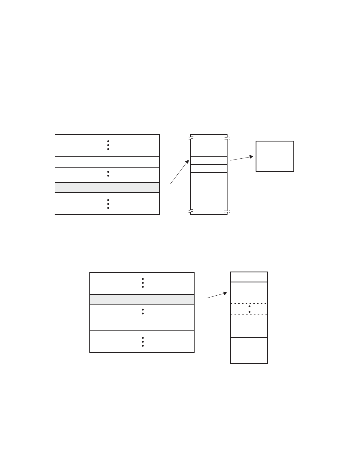
5 ExCA Compatibility Registers
The ExCA registers implemented in the PCI1510 controller are register-compatible with the Intel 82365SL−DF
PCMCIA controller. ExCA registers are identified by an offset value that is compatible with the legacy I/O index/data
scheme used on the Intel 82365 ISA controller . The ExCA registers are accessed through this scheme by writing the
register offset value into the index register (I/O base) and reading or writing the data register (I/O base + 1). The I/O
base address used in the index/data scheme is programmed in the PC Card 16-bit I/F legacy-mode base address
register (PCI offset 44h, see Section 4.28). The offsets from this base address run contiguously from 00h to 3Fh. See
Figure 5−1 for an ExCA I/O mapping illustration.
PCI1510 Configuration Registers
CardBus Socket/ExCA Base Address
Offset
10h
Host I/O Space
Index
Data
Offset
00h
PC Card A
ExCA
Registers
3Fh
16-Bit Legacy-Mode Base Address
44h
Figure 5−1. ExCA Register Access Through I/O
The controller also provides a memory-mapped alias of the ExCA registers by directly mapping them into PCI memory
space. They are located through the CardBus socket/ExCA base-address register (PCI offset 10h, see Section 4.12)
at memory offset 800h. See Figure 5−2 for an ExCA memory mapping illustration. This illustration also identifies the
CardBus socket register mapping, which is mapped into the same 4-K window at memory offset 00h.
Host
PCI1510 Configuration Registers
CardBus Socket/ExCA Base Address
16-Bit Legacy-Mode Base Address
10h
44h
Memory Space
CardBus
Socket
Registers
ExCA
Registers
OffsetOffset
00h
20h
800h
844h
Figure 5−2. ExCA Register Access Through Memory
The interrupt registers in the ExCA register set, as defined by the 82365SL−DL specification, control such card
functions as reset, type, interrupt routing, and interrupt enables. Special attention must be paid to the interrupt routing
registers and the host interrupt signaling method selected for the controller to ensure that all possible interrupts can
potentially be routed to the programmable interrupt controller. The ExCA registers that are critical to the interrupt
5−1

signaling are the ExCA interrupt and general control register (ExCA offset 03h/43h/803h, see Section 5.4) and the
ExCA card status-change interrupt configuration register (05h/45h/805h, see Section 5.6).
Access to I/O mapped 16-bit PC cards is available to the host system via two ExCA I/O windows. These are regions
of host I/O address space into which the card I/O space is mapped. These windows are defined by start, end, and
offset addresses programmed in the ExCA registers described in this section. I/O windows have byte granularity.
Access to memory mapped 16-bit PC Cards is available to the host system via five ExCA memory windows. These
are regions of host memory space into which the card memory space is mapped. These windows are defined by start,
end, and offset addresses programmed in the ExCA registers described in this section. Table 5−1 identifies each
ExCA register and its respective ExCA offset. Memory windows have 4-Kbyte granularity.
Table 5−1. ExCA Registers and Offsets
EXCA REGISTER NAME
Identification and revision 800 00
Interface status 801 01
Power control 802 02
Interrupt and general control 803 03
Card status change 804 04
Card status-change interrupt configuration 805 05
Address window enable 806 06
I / O window control 807 07
I / O window 0 start-address low byte 808 08
I / O window 0 start-address high byte 809 09
I / O window 0 end-address low byte 80A 0A
I / O window 0 end-address high byte 80B 0B
I / O window 1 start-address low byte 80C 0C
I / O window 1 start-address high byte 80D 0D
I / O window 1 end-address low byte 80E 0E
I / O window 1 end-address high byte 80F 0F
Memory window 0 start-address low byte 810 10
Memory window 0 start-address high byte 811 11
Memory window 0 end-address low byte 812 12
Memory window 0 end-address high byte 813 13
Memory window 0 offset-address low byte 814 14
Memory window 0 offset-address high byte 815 15
Card detect and general control 816 16
Reserved 817 17
Memory window 1 start-address low byte 818 18
Memory window 1 start-address high byte 819 19
Memory window 1 end-address low byte 81A 1A
Memory window 1 end-address high byte 81B 1B
Memory window 1 offset-address low byte 81C 1C
Memory window 1 offset-address high byte 81D 1D
Global control 81E 1E
Reserved 81F 1F
Memory window 2 start-address low byte 820 20
Memory window 2 start-address high byte 821 21
Memory window 2 end-address low byte 822 22
PCI MEMORY ADDRESS
OFFSET (HEX)
ExCA OFFSET
(HEX)
5−2

Table 5−1. ExCA Registers and Offsets (Continued)
EXCA REGISTER NAME
Memory window 2 end-address high byte 823 23
Memory window 2 offset-address low byte 824 24
Memory window 2 offset-address high byte 825 25
Reserved 826 26
Reserved 827 27
Memory window 3 start-address low byte 828 28
Memory window 3 start-address high byte 829 29
Memory window 3 end-address low byte 82A 2A
Memory window 3 end-address high byte 82B 2B
Memory window 3 offset-address low byte 82C 2C
Memory window 3 offset-address high byte 82D 2D
Reserved 82E 2E
Reserved 82F 2F
Memory window 4 start-address low byte 830 30
Memory window 4 start-address high byte 831 31
Memory window 4 end-address low byte 832 32
Memory window 4 end-address high byte 833 33
Memory window 4 offset-address low byte 834 34
Memory window 4 offset-address high byte 835 35
I/O window 0 offset-address low byte 836 36
I/O window 0 offset-address high byte 837 37
I/O window 1 offset-address low byte 838 38
I/O window 1 offset-address high byte 839 39
Reserved 83A 3A
Reserved 83B 3B
Reserved 83C 3C
Reserved 83D 3D
Reserved 83E 3E
Reserved 83F 3F
Memory window page 0 840 −
Memory window page 1 841 −
Memory window page 2 842 −
Memory window page 3 843 −
Memory window page 4 844 −
PCI MEMORY ADDRESS
OFFSET (HEX)
ExCA OFFSET
(HEX)
A bit description table, typically included when a register contains bits of more than one type or purpose, indicates
bit field names, which appear in the signal column; a detailed field description, which appears in the function column;
and field access tags, which appear in the type column of the bit description table. Table 4−2 describes the field
access tags.
5−3

5.1 ExCA Identification and Revision Register
The ExCA identification and revision register provides host software with information on 16-bit PC Card support and
Intel 82365SL-DF compatibility. This register is read-only or read/write, depending on the setting of bit 5
(SUBSYSRW) in the system control register (PCI offset 80h, see Section 4.29). See Table 5−2 for a complete
description of the register contents.
Bit 7 6 5 4 3 2 1 0
Default 1 0 0 0 0 1 0 0
Register: ExCA identification and revision
Offset: CardBus socket address + 800h; ExCA offset 00h
Type: Read-only, Read/Write
Default: 84h
Table 5−2. ExCA Identification and Revision Register Description
BIT SIGNAL TYPE FUNCTION
7−6 IFTYPE R
5−4 RSVD RW Reserved. Bits 5 and 4 can be used for Intel 82365SL-DF emulation.
3−0 365REV RW
Interface type. These bits, which are hardwired as 10b, identify the 16-bit PC Card support provided by the
controller. The controller supports both I/O and memory 16-bit PC cards.
Intel 82365SL-DF revision. This field stores the Intel 82365SL-DF revision supported by the controller. Host
software can read this field to determine compatibility to the Intel
this field puts the controller in 82365SL mode.
82365SL-DF register set. Writing 0010b to
5−4

5.2 ExCA Interface Status Register
The ExCA interface status register provides information on the current status of the PC Card interface. An X in the
default bit value indicates that the value of the bit after reset depends on the state of the PC Card interface. See
Table 5−3 for a complete description of the register contents.
Bit 7 6 5 4 3 2 1 0
Default 0 0 X X X X X X
Register: ExCA interface status
Offset: CardBus socket address + 801h; ExCA offset 01h
Type: Read-only
Default: 00XX XXXXb
Table 5−3. ExCA Interface Status Register Description
BIT SIGNAL TYPE FUNCTION
7 RSVD R Reserved. Bit 7 returns 0b when read.
Card Power. Bit 6 indicates the current power status of the PC Card socket. This bit reflects how the ExCA
6 CARDPWR R
5 READY R
4 CARDWP R
3 CDETECT2 R
2 CDETECT1 R
1−0 BVDSTAT R
power control register (ExCA offset 02h/42h/802h, see Section 5.3) is programmed. Bit 6 is encoded as:
0 = VCC and VPP to the socket turned off (default)
1 = VCC and VPP to the socket turned on
Ready. Bit 5 indicates the current status of the READY signal at the PC Card interface.
0 = PC Card not ready for data transfer
1 = PC Card ready for data transfer
Card write protect (WP). Bit 4 indicates the current status of WP at the PC Card interface. This signal reports
to the controller whether or not the memory card is write protected. Furthermore, write protection for an entire
16-bit memory window is available by setting the appropriate bit in the memory window offset-address
high-byte register.
0 = WP is 0b. PC Card is read/write.
1 = WP is 1b. PC Card is read-only.
Card detect 2. Bit 3 indicates the status of CD2 at the PC Card interface. Software may use this and bit 2
(CDETECT1) to determine if a PC Card is fully seated in the socket.
0 = CD2 is 1b. No PC Card is inserted.
1 = CD2
is 0b. PC Card is at least partially inserted.
Card detect 1. Bit 2 indicates the status of CD1 at the PC Card interface. Software may use this and bit 3
(CDETECT2) to determine if a PC Card is fully seated in the socket.
0 = CD1 is 1b. No PC Card is inserted.
1 = CD1
is 0b. PC Card is at least partially inserted.
Battery voltage detect. When a 16-bit memory card is inserted, the field indicates the status of the battery
voltage detect signals (BVD1, BVD2) at the PC Card interface, where bit 1 reflects the BVD2 status and bit 0
reflects BVD1.
00 = Battery dead
01 = Battery dead
10 = Battery low; warning
11 = Battery good
When a 16-bit I/O card is inserted, this field indicates the status of SPKR
PC Card interface. In this case, the two bits in this field directly reflect the current state of these card outputs.
(bit 1) and STSCHG (bit 0) at the
5−5

5.3 ExCA Power Control Register
The ExCA power control register provides PC Card power control. Bit 7 (COE) of this register controls the 16-bit output
enables on the socket interface, and can be used for power management in 16-bit PC Card applications. See
Table 5−4 and Table 5−5 for a complete description of the register contents.
The controller supports both the 82365SL and 82365SL-DF register models. Bits 3−0 (365REV) of the ExCA
identification and revision register (ExCA offset 00h, see Section 5.1) control which register model is supported.
Bit 7 6 5 4 3 2 1 0
Default 0 0 0 0 0 0 0 0
Register: ExCA power control—82365SL support
Offset: CardBus socket address + 802h; ExCA offset 02h
Type: Read-only, Read/Write
Default: 00h
Table 5−4. ExCA Power Control Register Description—82365SL Support
BIT SIGNAL TYPE FUNCTION
Card output enable. Bit 7 controls the state of all of the 16-bit outputs on the controller. This bit is
7 COE RW
6 RSVD R Reserved. Bit 6 returns 0b when read.
5 AUTOPWRSWEN RW
4 CAPWREN RW
3−2 RSVD R Reserved. Bits 3 and 2 return 00b when read.
1−0 EXCAVPP RW
encoded as:
0 = 16-bit PC Card outputs disabled (default)
1 = 16-bit PC Card outputs enabled
Auto power switch enable.
0 = Automatic socket power switching based on card detects is disabled
1 = Automatic socket power switching based on card detects is enabled
PC Card power enable.
0 = VCC = No connection
1 = VCC is enabled and controlled by bit 2 (EXCAPOWER) of the system control register
(PCI offset 80h, see Section 4.29)
PC Card VPP power control. Bits 1 and 0 request changes to card VPP. The controller ignores this field
unless VCC to the socket is enabled. This field is encoded as:
00 = No connection (default)
01 = V
CC
10 = 12 V
11 = Reserved
5−6

Bit
Default 0 0 0 0 0 0 0 0
7 6 5 4 3 2 1 0
Register: ExCA power control—82365SL-DF support
Offset: CardBus socket address + 802h; ExCA offset 02h
Type: Read-only, Read/Write
Default: 00h
Table 5−5. ExCA Power Control Register Description—82365SL-DF Support
BIT SIGNAL TYPE FUNCTION
Card output enable. Bit 7 controls the state of all of the 16-bit outputs on the controller . This bit is encoded as:
7 COE RW
6−5 RSVD R Reserved. Bits 6 and 5 return 00b when read.
4−3 EXCAVCC RW
2 RSVD R Reserved. Bit 2 returns 0b when read.
1−0 EXCAVPP RW
0 = 16-bit PC Card outputs disabled (default)
1 = 16-bit PC Card outputs enabled
VCC. Bits 4 and 3 request changes to card VCC. This field is encoded as:
00 = 0 V (default)
01 = 0 V reserved
10 = 5 V
11 = 3.3 V
VPP. Bits 1 and 0 request changes to card VPP. The controller ignores this field unless VCC to the socket is
enabled. This field is encoded as:
00 = No connection (default)
01 = V
CC
10 = 12 V
11 = Reserved
5−7

5.4 ExCA Interrupt and General Control Register
The ExCA interrupt and general control register controls interrupt routing for I/O interrupts, as well as other critical
16-bit PC Card functions. See Table 5−6 for a complete description of the register contents.
Bit 7 6 5 4 3 2 1 0
Default 0 0 0 0 0 0 0 0
Register: ExCA interrupt and general control
Offset: CardBus socket address + 803h; ExCA offset 03h
Type: Read/Write
Default: 00h
Table 5−6. ExCA Interrupt and General Control Register Description
BIT SIGNAL TYPE FUNCTION
Card ring indicate enable. Bit 7 enables the ring indicate function of BVD1/RI. This bit is encoded as:
7 RINGEN RW
6 RESET RW
5 CARDTYPE RW
4 CSCROUTE RW
3−0 INTSELECT RW
0 = Ring indicate disabled (default)
1 = Ring indicate enabled
Card reset. Bit 6 controls the 16-bit PC Card RESET, and allows host software to force a card reset. Bit 6
affects 16-bit cards only. This bit is encoded as:
0 = RESET signal asserted (default)
1 = RESET signal deasserted
Card type. Bit 5 indicates the PC card type. This bit is encoded as:
0 = Memory PC Card installed (default)
1 = I/O PC Card installed
PCI interrupt CSC routing enable bit. When bit 4 is set (high), the card status change interrupts are routed
to PCI interrupts. When low, the card status change interrupts are routed using bits 7−4 (CSCSELECT field)
in the ExCA card status-change interrupt configuration register (ExCA offset 05h/45h/805h, see
Section 5.6). This bit is encoded as:
0 = CSC interrupts are routed by ExCA registers (default)
1 = CSC interrupts are routed to PCI interrupts
Card interrupt select for I/O PC Card functional interrupts. Bits 3−0 select the interrupt routing for I/O
PC Card functional interrupts. This field is encoded as:
0000 = No interrupt routing (default). CSC interrupts are routed to PCI interrupts. This bit setting is
ORed with bit 4 (CSCROUTE) for backward compatibility.
0001 = IRQ1 enabled
0010 = SMI enabled
0011 = IRQ3 enabled
0100 = IRQ4 enabled
0101 = IRQ5 enabled
0100 = IRQ6 enabled
0111 = IRQ7 enabled
1000 = IRQ8 enabled
1001 = IRQ9 enabled
1010 = IRQ10 enabled
1011 = IRQ11 enabled
1100 = IRQ12 enabled
1101 = IRQ13 enabled
1110 = IRQ14 enabled
1111 = IRQ15 enabled
5−8

5.5 ExCA Card Status-Change Register
The ExCA card status-change register controls interrupt routing for I/O interrupts as well as other critical 16-bit PC
Card functions. The register enables these interrupt sources to generate an interrupt to the host. When the interrupt
source is disabled, the corresponding bit in this register always reads 0b. When an interrupt source is enabled, the
corresponding bit in this register is set to indicate that the interrupt source is active. After generating the interrupt to
the host, the interrupt service routine must read this register to determine the source of the interrupt. The interrupt
service routine is responsible for resetting the bits in this register as well. Resetting a bit is accomplished by one of
two methods: a read of this register or an explicit write back of 1b to the status bit. The choice of these two methods
is based on bit 2 (interrupt flag clear mode select) in the ExCA global control register (ExCA offset 1E/5E/81E, see
Section 5.20). See Table 5−7 for a complete description of the register contents.
Bit 7 6 5 4 3 2 1 0
Default 0 0 0 0 0 0 0 0
Register: ExCA card status-change
Offset: CardBus socket address + 804h; ExCA offset 04h
Type: Read-only
Default: 00h
Table 5−7. ExCA Card Status-Change Register Description
BIT SIGNAL TYPE FUNCTION
7−4 RSVD R Reserved. Bits 7−4 return 0h when read.
Card detect change. Bit 3 indicates whether a change on CD1 or CD2 occurred at the PC Card interface.
3 CDCHANGE R
2 READYCHANGE R
1 BATWARN R
0 BATDEAD R
This bit is encoded as:
0 = No change detected on either CD1 or CD2
1 = Change detected on either CD1 or CD2
Ready change. When a 16-bit memory is installed in the socket, bit 2 includes whether the source of an
interrupt was due to a change on READY at the PC Card interface, indicating that the PC Card is now
ready to accept new data. This bit is encoded as:
0 = No low-to-high transition detected on READY (default)
1 = Detected low-to-high transition on READY
When a 16-bit I/O card is installed, bit 2 is always 0b.
Battery warning change. When a 16-bit memory card is installed in the socket, bit 1 indicates whether the
source of an interrupt was due to a battery-low warning condition. This bit is encoded as:
0 = No battery warning condition (default)
1 = Detected battery warning condition
When a 16-bit I/O card is installed, bit 1 is always 0b.
Battery dead or status change. When a 16-bit memory card is installed in the socket, bit 0 indicates
whether the source of an interrupt was due to a battery dead condition. This bit is encoded as:
0 = STSCHG deasserted (default)
1 = STSCHG
Ring indicate. When the controller is configured for ring indicate operation, bit 0 indicates the status of
RI
.
asserted
5−9

5.6 ExCA Card Status-Change Interrupt Configuration Register
The ExCA card status-change interrupt configuration register controls interrupt routing for card status-change
interrupts, as well as masking CSC interrupt sources. See Table 5−8 for a complete description of the register
contents.
Bit 7 6 5 4 3 2 1 0
Default 0 0 0 0 0 0 0 0
Register: ExCA card status-change interrupt configuration
Offset: CardBus socket address + 805h; ExCA offset 05h
Type: Read/Write
Default: 00h
Table 5−8. ExCA Card Status-Change Interrupt Configuration Register Description
BIT SIGNAL TYPE FUNCTION
Interrupt select for card status change. Bits 7−4 select the interrupt routing for card status-change
interrupts.
0000 = CSC interrupts routed to PCI interrupts if bit 5 (CSC) of the diagnostic register (PCI of fset 93h, see
Section 4.34) is set to 1b. In this case bit 4 (CSCROUTE) of the ExCA interrupt and general control register
(ExCA offset 03h/43h/803h, see Section 5.4) is a don’t care. This is the default setting.
0000 = No ISA interrupt routing if bit 5 (CSC) of the diagnostic register is set to 0b (see Section 4.34). In
this case, CSC interrupts are routed to PCI interrupts by setting bit 4 (CSCROUTE) of the ExCA interrupt
7−4 CSCSELECT RW
3 CDEN RW
2 READYEN RW
1 BATWARNEN RW
0 BATDEADEN RW
and general control register (ExCA offset 03h/43h/803h, see Section 5.4) to 1b.
This field is encoded as:
0000 = No interrupt routing (default) 1000 = IRQ8 enabled
0001 = IRQ1 enabled 1001 = IRQ9 enabled
0010 = SMI enabled 1010 = IRQ10 enabled
0011 = IRQ3 enabled 1011 = IRQ11 enabled
0100 = IRQ4 enabled 1100 = IRQ12 enabled
0101 = IRQ5 enabled 1101 = IRQ13 enabled
0110 = IRQ6 enabled 1110 = IRQ14 enabled
0111 = IRQ7 enabled 1111 = IRQ15 enabled
Card detect enable. Bit 3 enables interrupts on CD1 or CD2 changes. This bit is encoded as:
0 = Disables interrupts on CD1
1 = Enables interrupts on CD1
Ready enable. Bit 2 enables/disables a low-to-high transition on PC Card READY to generate a host
interrupt. This interrupt source is considered a card status change. This bit is encoded as:
0 = Disables host interrupt generation (default)
1 = Enables host interrupt generation
Battery warning enable. Bit 1 enables/disables a battery warning condition to generate a CSC interrupt.
This bit is encoded as:
0 = Disables host interrupt generation (default)
1 = Enables host interrupt generation
Battery dead enable. Bit 0 enables/disables a battery dead condition on a memory PC Card or assertion
of the STSCHG
0 = Disables host interrupt generation (default)
1 = Enables host interrupt generation
I/O PC Card signal to generate a CSC interrupt.
or CD2 line changes (default)
or CD2 line changes
5−10
 Loading...