

Texas Instruments PCI1451AGJG, PCI1451GJG Datasheet

1999 PCIBus Solutions
Data Manual

Printed in U.S.A.
11/99
SCPS054

PCI1451
PC Card Controller
Data Manual
Literature Number: SCPS054
November 1999
Printed on Recycled Paper

IMPORTANT NOTICE
Texas Instruments and its subsidiaries (TI) reserve the right to make changes to their products
or to discontinue any product or service without notice, and advise customers to obtain the latest
version of relevant information to verify, before placing orders, that information being relied on
is current and complete. All products are sold subject to the terms and conditions of sale supplied
at the time of order acknowledgement, including those pertaining to warranty, patent
infringement, and limitation of liability.
TI warrants performance of its semiconductor products to the specifications applicable at the
time of sale in accordance with TI’s standard warranty. Testing and other quality control
techniques are utilized to the extent TI deems necessary to support this warranty. Specific testing
of all parameters of each device is not necessarily performed, except those mandated by
government requirements.
CERTAIN APPLICATIONS USING SEMICONDUCTOR PRODUCTS MAY INVOLVE
POTENTIAL RISKS OF DEATH, PERSONAL INJURY, OR SEVERE PROPERTY OR
ENVIRONMENTAL DAMAGE (“CRITICAL APPLICATIONS”). TI SEMICONDUCTOR
PRODUCTS ARE NOT DESIGNED, AUTHORIZED, OR WARRANTED TO BE SUIT ABLE FOR
USE IN LIFE-SUPPORT DEVICES OR SYSTEMS OR OTHER CRITICAL APPLICATIONS.
INCLUSION OF TI PRODUCTS IN SUCH APPLICATIONS IS UNDERSTOOD TO BE FULLY
AT THE CUSTOMER’S RISK.
In order to minimize risks associated with the customer’s applications, adequate design and
operating safeguards must be provided by the customer to minimize inherent or procedural
hazards.
TI assumes no liability for applications assistance or customer product design. TI does not
warrant or represent that any license, either express or implied, is granted under any patent right,
copyright, mask work right, or other intellectual property right of TI covering or relating to any
combination, machine, or process in which such semiconductor products or services might be
or are used. TI’s publication of information regarding any third party’s products or services does
not constitute TI’s approval, warranty or endorsement thereof.
Copyright 1999, Texas Instruments Incorporated

iii
Contents
Section Title Page
1 Introduction 1–1. . . . . . . . . . . . . . . . . . . . . . . . . . . . . . . . . . . . . . . . . . . . . . . . . . . . .
1.1 Description 1–1. . . . . . . . . . . . . . . . . . . . . . . . . . . . . . . . . . . . . . . . . . . . . . . . .
1.2 Features 1–1. . . . . . . . . . . . . . . . . . . . . . . . . . . . . . . . . . . . . . . . . . . . . . . . . . .
1.3 Related Documents 1–2. . . . . . . . . . . . . . . . . . . . . . . . . . . . . . . . . . . . . . . . . .
1.4 Ordering Information 1–2. . . . . . . . . . . . . . . . . . . . . . . . . . . . . . . . . . . . . . . . .
2 Terminal Descriptions 2–1. . . . . . . . . . . . . . . . . . . . . . . . . . . . . . . . . . . . . . .
3 Feature/Protocol Descriptions 3–1. . . . . . . . . . . . . . . . . . . . . . . . . . . . . . .
3.1 I/O Characteristics 3–1. . . . . . . . . . . . . . . . . . . . . . . . . . . . . . . . . . . . . . . . . . .
3.2 Clamping Voltages 3–2. . . . . . . . . . . . . . . . . . . . . . . . . . . . . . . . . . . . . . . . . .
3.3 Peripheral Component Interconnect (PCI) Interface 3–2. . . . . . . . . . . . . .
3.3.1 PCI Bus Lock (LOCK
) 3–2. . . . . . . . . . . . . . . . . . . . . . . . . . . . . . .
3.3.2 Loading The Subsystem Identification
(EEPROM Interface) 3–3. . . . . . . . . . . . . . . . . . . . . . . . . . . . . . . .
3.3.3 Serial Bus EEPROM Application 3–5. . . . . . . . . . . . . . . . . . . . . .
3.4 PC Card Applications Overview 3–6. . . . . . . . . . . . . . . . . . . . . . . . . . . . . . .
3.4.1 PC Card Insertion/Removal and Recognition 3–6. . . . . . . . . . .
3.4.2 P
2
C Power Switch Interface (TPS2202A/2206) 3–7. . . . . . . . .
3.4.3 Zoomed Video Support 3–8. . . . . . . . . . . . . . . . . . . . . . . . . . . . . .
3.4.4 Zoomed Video Auto Detect 3–9. . . . . . . . . . . . . . . . . . . . . . . . . .
3.4.5 Ultra Zoomed Video 3–11. . . . . . . . . . . . . . . . . . . . . . . . . . . . . . . . .
3.4.6 D3_STAT
Terminal 3–11. . . . . . . . . . . . . . . . . . . . . . . . . . . . . . . . .
3.4.7 Internal Ring Oscillator 3–11. . . . . . . . . . . . . . . . . . . . . . . . . . . . . .
3.4.8 Integrated Pullup Resistors 3–12. . . . . . . . . . . . . . . . . . . . . . . . . .
3.4.9 SPKROUT Usage 3–12. . . . . . . . . . . . . . . . . . . . . . . . . . . . . . . . . . .
3.4.10 LED Socket Activity Indicators 3–13. . . . . . . . . . . . . . . . . . . . . . . .
3.4.11 PC Card 16 DMA Support 3–13. . . . . . . . . . . . . . . . . . . . . . . . . . .
3.4.12 CardBus Socket Registers 3–14. . . . . . . . . . . . . . . . . . . . . . . . . . .
3.5 Programmable Interrupt Subsystem 3–14. . . . . . . . . . . . . . . . . . . . . . . . . . . .
3.5.1 PC Card Functional And Card Status Change Interrupts 3–15.
3.5.2 Interrupt Masks And Flags 3–16. . . . . . . . . . . . . . . . . . . . . . . . . . .
3.5.3 Using Parallel PCI Interrupts 3–16. . . . . . . . . . . . . . . . . . . . . . . . .
3.6 Power Management Overview 3–17. . . . . . . . . . . . . . . . . . . . . . . . . . . . . . . .
3.6.1 CLKRUN
Protocol 3–17. . . . . . . . . . . . . . . . . . . . . . . . . . . . . . . . . .
3.6.2 CardBus PC Card Power Management 3–17. . . . . . . . . . . . . . . .
3.6.3 PCI Bus Power Management 3–17. . . . . . . . . . . . . . . . . . . . . . . . .
3.6.4 CardBus Device Class Power Management 3–18. . . . . . . . . . . .
3.6.5 Master List Of PME
Context Bits and Global
Reset Only Bits 3–18. . . . . . . . . . . . . . . . . . . . . . . . . . . . . . . . . . . .

iv
3.6.6 System Diagram Implementing CardBus Device Class
Power Management 3–19. . . . . . . . . . . . . . . . . . . . . . . . . . . . . . . .
3.6.7 Suspend Mode 3–20. . . . . . . . . . . . . . . . . . . . . . . . . . . . . . . . . . . . .
3.6.8 Requirements For SUSPEND
3–20. . . . . . . . . . . . . . . . . . . . . . . .
3.6.9 Ring Indicate 3–20. . . . . . . . . . . . . . . . . . . . . . . . . . . . . . . . . . . . . . .
4 PC Card Controller Programming Model 4–1. . . . . . . . . . . . . . . . . . . . . .
4.1 PCI Configuration Registers (Functions 0 and 1) 4–1. . . . . . . . . . . . . . . . .
4.2 Vendor ID Register 4–2. . . . . . . . . . . . . . . . . . . . . . . . . . . . . . . . . . . . . . . . . .
4.3 Device ID Register 4–2. . . . . . . . . . . . . . . . . . . . . . . . . . . . . . . . . . . . . . . . . . .
4.4 Command Register 4–3. . . . . . . . . . . . . . . . . . . . . . . . . . . . . . . . . . . . . . . . . .
4.5 Status Register 4–4. . . . . . . . . . . . . . . . . . . . . . . . . . . . . . . . . . . . . . . . . . . . . .
4.6 Revision ID Register 4–5. . . . . . . . . . . . . . . . . . . . . . . . . . . . . . . . . . . . . . . . .
4.7 PCI Class Code Register 4–5. . . . . . . . . . . . . . . . . . . . . . . . . . . . . . . . . . . . .
4.8 Cache Line Size Register 4–5. . . . . . . . . . . . . . . . . . . . . . . . . . . . . . . . . . . . .
4.9 Latency Timer Register 4–6. . . . . . . . . . . . . . . . . . . . . . . . . . . . . . . . . . . . . .
4.10 Header Type Register 4–6. . . . . . . . . . . . . . . . . . . . . . . . . . . . . . . . . . . . . . . .
4.11 BIST Register 4–6. . . . . . . . . . . . . . . . . . . . . . . . . . . . . . . . . . . . . . . . . . . . . . .
4.12 CardBus Socket/ExCA Base-Address Register 4–7. . . . . . . . . . . . . . . . . .
4.13 Capability Pointer Register 4–7. . . . . . . . . . . . . . . . . . . . . . . . . . . . . . . . . . . .
4.14 Secondary Status Register 4–8. . . . . . . . . . . . . . . . . . . . . . . . . . . . . . . . . . .
4.15 PCI Bus Number Register 4–9. . . . . . . . . . . . . . . . . . . . . . . . . . . . . . . . . . . .
4.16 CardBus Bus Number Register 4–9. . . . . . . . . . . . . . . . . . . . . . . . . . . . . . . .
4.17 Subordinate Bus Number Register 4–9. . . . . . . . . . . . . . . . . . . . . . . . . . . . .
4.18 CardBus Latency Timer Register 4–10. . . . . . . . . . . . . . . . . . . . . . . . . . . . . .
4.19 Memory Base Registers 0, 1 4–10. . . . . . . . . . . . . . . . . . . . . . . . . . . . . . . . . .
4.20 Memory Limit Registers 0, 1 4–11. . . . . . . . . . . . . . . . . . . . . . . . . . . . . . . . . .
4.21 I/O Base Registers 0, 1 4–11. . . . . . . . . . . . . . . . . . . . . . . . . . . . . . . . . . . . . . .
4.22 I/O Limit Registers 0, 1 4–12. . . . . . . . . . . . . . . . . . . . . . . . . . . . . . . . . . . . . .
4.23 Interrupt Line Register 4–12. . . . . . . . . . . . . . . . . . . . . . . . . . . . . . . . . . . . . . .
4.24 Interrupt Pin Register 4–13. . . . . . . . . . . . . . . . . . . . . . . . . . . . . . . . . . . . . . . .
4.25 Bridge Control Register 4–14. . . . . . . . . . . . . . . . . . . . . . . . . . . . . . . . . . . . . .
4.26 Subsystem Vendor ID Register 4–15. . . . . . . . . . . . . . . . . . . . . . . . . . . . . . .
4.27 Subsystem ID Register 4–15. . . . . . . . . . . . . . . . . . . . . . . . . . . . . . . . . . . . . . .
4.28 PC Card 16-Bit I/F Legacy Mode Base Address Register 4–16. . . . . . . . .
4.29 System Control Register 4–17. . . . . . . . . . . . . . . . . . . . . . . . . . . . . . . . . . . . . .
4.30 Multimedia Control Register 4–20. . . . . . . . . . . . . . . . . . . . . . . . . . . . . . . . . .
4.31 General Status Register 4–21. . . . . . . . . . . . . . . . . . . . . . . . . . . . . . . . . . . . . .
4.32 General-Purpose Event Status Register 4–22. . . . . . . . . . . . . . . . . . . . . . . .
4.33 General-Purpose Event Enable Register 4–22. . . . . . . . . . . . . . . . . . . . . . .
4.34 General-Purpose Input Register 4–23. . . . . . . . . . . . . . . . . . . . . . . . . . . . . . .
4.35 General-Purpose Output Register 4–23. . . . . . . . . . . . . . . . . . . . . . . . . . . . .
4.36 Multifunction Routing Status Register 4–24. . . . . . . . . . . . . . . . . . . . . . . . . .
4.37 Retry Status Register 4–26. . . . . . . . . . . . . . . . . . . . . . . . . . . . . . . . . . . . . . . .
4.38 Card Control Register 4–27. . . . . . . . . . . . . . . . . . . . . . . . . . . . . . . . . . . . . . . .

v
4.39 Device Control Register 4–28. . . . . . . . . . . . . . . . . . . . . . . . . . . . . . . . . . . . . .
4.40 Diagnostic Register 4–29. . . . . . . . . . . . . . . . . . . . . . . . . . . . . . . . . . . . . . . . . .
4.41 Socket DMA Register 0 4–30. . . . . . . . . . . . . . . . . . . . . . . . . . . . . . . . . . . . . .
4.42 Socket DMA Register 1 4–31. . . . . . . . . . . . . . . . . . . . . . . . . . . . . . . . . . . . . .
4.43 Capability ID Register 4–32. . . . . . . . . . . . . . . . . . . . . . . . . . . . . . . . . . . . . . . .
4.44 Next Item Pointer Register 4–32. . . . . . . . . . . . . . . . . . . . . . . . . . . . . . . . . . . .
4.45 Power Management Capabilities Register 4–33. . . . . . . . . . . . . . . . . . . . . .
4.46 Power Management Control/Status Register 4–34. . . . . . . . . . . . . . . . . . . .
4.47 Power Management Control/Status Register Bridge
Support Extensions 4–35. . . . . . . . . . . . . . . . . . . . . . . . . . . . . . . . . . . . . . . . .
4.48 General-Purpose Event Control/Status Register 4–36. . . . . . . . . . . . . . . . .
5 ExCA Compatibility Registers (Functions 0 and 1) 5–1. . . . . . . . . . . . .
5.1 ExCA Identification and Revision Register (Index 00h) 5–5. . . . . . . . . . .
5.2 ExCA Interface Status Register (Index 01h) 5–6. . . . . . . . . . . . . . . . . . . . .
5.3 ExCA Power Control Register (Index 02h) 5–7. . . . . . . . . . . . . . . . . . . . . .
5.4 ExCA Interrupt and General Control Register (Index 03h) 5–8. . . . . . . . .
5.5 ExCA Card Status-Change Register (Index 04h) 5–9. . . . . . . . . . . . . . . . .
5.6 ExCA Card Status-Change Interrupt Configuration Register
(Index 05h) 5–10. . . . . . . . . . . . . . . . . . . . . . . . . . . . . . . . . . . . . . . . . . . . . . . . .
5.7 ExCA Address Window Enable Register (Index 06h) 5–11. . . . . . . . . . . . .
5.8 ExCA I/O Window Control Register (Index 07h) 5–12. . . . . . . . . . . . . . . . .
5.9 ExCA I/O Windows 0 and 1 Start-Address Low-Byte Registers
(Index 08h, 0Ch) 5–13. . . . . . . . . . . . . . . . . . . . . . . . . . . . . . . . . . . . . . . . . . . .
5.10 ExCA I/O Windows 0 and 1 Start-Address High-Byte Registers
(Index 09h, ODh) 5–13. . . . . . . . . . . . . . . . . . . . . . . . . . . . . . . . . . . . . . . . . . .
5.11 ExCA I/O Windows 0 and 1 End-Address Low-Byte Registers
(Index 0Ah, 0Eh) 5–14. . . . . . . . . . . . . . . . . . . . . . . . . . . . . . . . . . . . . . . . . . . .
5.12 ExCA I/O Windows 0 and 1 End-Address High-Byte Registers
(Index 0Bh, 0Fh) 5–14. . . . . . . . . . . . . . . . . . . . . . . . . . . . . . . . . . . . . . . . . . . .
5.13 ExCA Memory Windows 0–4 Start-Address Low-Byte
Registers (Index 10h/18h/20h/28h/30h) 5–15. . . . . . . . . . . . . . . . . . . . . . . .
5.14 ExCA Memory Windows 0–4 Start-Address High-Byte
Registers (Index 11h/19h/21h/29h/31h) 5–16. . . . . . . . . . . . . . . . . . . . . . . .
5.15 ExCA Memory Windows 0–4 End-Address Low-Byte Registers
(Index 12h/1Ah/22h/2Ah/32h) 5–17. . . . . . . . . . . . . . . . . . . . . . . . . . . . . . . .
5.16 ExCA Memory Windows 0–4 End-Address High-Byte Registers
(Index 13h/1Bh/23h/2Bh/33h) 5–18. . . . . . . . . . . . . . . . . . . . . . . . . . . . . . . .
5.17 ExCA Memory Windows 0–4 Offset-Address Low-Byte Registers
(Index 14h/1Ch/24h/2Ch/34h) 5–19. . . . . . . . . . . . . . . . . . . . . . . . . . . . . . . .
5.18 ExCA Memory Windows 0–4 Offset-Address High-Byte Registers
(Index 15h/1Dh/25h/2Dh/35h) 5–20. . . . . . . . . . . . . . . . . . . . . . . . . . . . . . . .
5.19 ExCA I/O Windows 0 and 1 Offset-Address Low-Byte Registers
(Index 36h, 38h) 5–21. . . . . . . . . . . . . . . . . . . . . . . . . . . . . . . . . . . . . . . . . . . .
5.20 ExCA I/O Windows 0 and 1 Offset-Address High-Byte Registers
(Index 37h, 39h) 5–21. . . . . . . . . . . . . . . . . . . . . . . . . . . . . . . . . . . . . . . . . . . .
5.21 ExCA Card Detect and General Control Register (Index 16h) 5–22. . . . . .
5.22 ExCA Global Control Register (Index 1Eh) 5–23. . . . . . . . . . . . . . . . . . . . . .

vi
5.23 ExCA Memory Windows 0–4 Page Registers (Index 40h, 41h,
42h, 43h, 44h) 5–24. . . . . . . . . . . . . . . . . . . . . . . . . . . . . . . . . . . . . . . . . . . . . .
6 CardBus Socket Registers (Functions 0 and 1) 6–1. . . . . . . . . . . . . . . .
6.1 Socket Event Register 6–2. . . . . . . . . . . . . . . . . . . . . . . . . . . . . . . . . . . . . . .
6.2 Socket Mask Register 6–3. . . . . . . . . . . . . . . . . . . . . . . . . . . . . . . . . . . . . . . .
6.3 Socket Present State Register 6–4. . . . . . . . . . . . . . . . . . . . . . . . . . . . . . . .
6.4 Socket Force Event Register 6–6. . . . . . . . . . . . . . . . . . . . . . . . . . . . . . . . . .
6.5 Socket Control Register 6–7. . . . . . . . . . . . . . . . . . . . . . . . . . . . . . . . . . . . . .
6.6 Socket Power Management Register 6–8. . . . . . . . . . . . . . . . . . . . . . . . . . .
7 Distributed DMA (DDMA) Registers 7–1. . . . . . . . . . . . . . . . . . . . . . . . . . .
7.1 DMA Current Address/Base Address Register 7–2. . . . . . . . . . . . . . . . . . .
7.2 DMA Page Register 7–2. . . . . . . . . . . . . . . . . . . . . . . . . . . . . . . . . . . . . . . . . .
7.3 DMA Current Count/Base Count Register 7–3. . . . . . . . . . . . . . . . . . . . . . .
7.4 DMA Command Register 7–3. . . . . . . . . . . . . . . . . . . . . . . . . . . . . . . . . . . .
7.5 DMA Status Register 7–4. . . . . . . . . . . . . . . . . . . . . . . . . . . . . . . . . . . . . . . . .
7.6 DMA Request Register 7–4. . . . . . . . . . . . . . . . . . . . . . . . . . . . . . . . . . . . . . .
7.7 DMA Mode Register 7–5. . . . . . . . . . . . . . . . . . . . . . . . . . . . . . . . . . . . . . . . .
7.8 DMA Master Clear Register 7–5. . . . . . . . . . . . . . . . . . . . . . . . . . . . . . . . . . .
7.9 DMA Multichannel Mask Register 7–6. . . . . . . . . . . . . . . . . . . . . . . . . . . . . .
8 Electrical Characteristics 8–1. . . . . . . . . . . . . . . . . . . . . . . . . . . . . . . . . . . .
8.1 Absolute Maximum Ratings Over Operating Temperature Ranges 8–1.
8.2 Recommended Operating Conditions 8–2. . . . . . . . . . . . . . . . . . . . . . . . . .
8.3 Electrical Characteristics Over Recommended
Operating Conditions 8–3. . . . . . . . . . . . . . . . . . . . . . . . . . . . . . . . . . . . . . . .
8.4 PCI Clock/Reset Timing Requirements Over
Recommended Ranges of Supply Voltage and Operating
Free-Air Temperature 8–3. . . . . . . . . . . . . . . . . . . . . . . . . . . . . . . . . . . . . . . .
8.5 PCI Timing Requirements Over Recommended Ranges of
Supply Voltage and Operating Free-Air Temperature 8–4. . . . . . . . . . . . .
8.6 Parameter Measurement Information 8–5. . . . . . . . . . . . . . . . . . . . . . . . . .
8.7 PCI Bus Parameter Measurement Information 8–6. . . . . . . . . . . . . . . . . . .
8.8 PC Card Cycle Timing 8–6. . . . . . . . . . . . . . . . . . . . . . . . . . . . . . . . . . . . . . .
8.9 Timing Requirements Over Recommended Ranges of
Supply Voltage and Operating Free-Air Temperature,
Memory Cycles 8–8. . . . . . . . . . . . . . . . . . . . . . . . . . . . . . . . . . . . . . . . . . . . .
8.10 Timing Requirements Over Recommended Ranges of
Supply Voltage and Operating Free-Air Temperature, I/O Cycles 8–8. . .
8.11 Switching Characteristics Over Recommended Ranges of
Supply Voltage and Operating Free-Air Temperature,
Miscellaneous 8–9. . . . . . . . . . . . . . . . . . . . . . . . . . . . . . . . . . . . . . . . . . . . . . .
8.12 PC Card Parameter Measurement Information 8–9. . . . . . . . . . . . . . . . . .
9 Mechanical Data 9–1. . . . . . . . . . . . . . . . . . . . . . . . . . . . . . . . . . . . . . . . . . . .

vii
List of Illustrations
Figure Title Page
2–1 PCI1451 GJG Terminal Diagram 2–1. . . . . . . . . . . . . . . . . . . . . . . . . . . . . . . . . .
3–1 PCI1451 System Block Diagram 3–1. . . . . . . . . . . . . . . . . . . . . . . . . . . . . . . . . .
3–2 3-State Bidirectional Buffer 3–2. . . . . . . . . . . . . . . . . . . . . . . . . . . . . . . . . . . . . . .
3–3 Serial EEPROM Application 3–3. . . . . . . . . . . . . . . . . . . . . . . . . . . . . . . . . . . . . .
3–4 EEPROM Interface Subsystem Data Collection 3–4. . . . . . . . . . . . . . . . . . . . .
3–5 Serial EEPROM Start/Stop Conditions and BIt Transfers 3–4. . . . . . . . . . . . .
3–6 Serial EEPROM Protocol – Acknowledge 3–5. . . . . . . . . . . . . . . . . . . . . . . . . .
3–7
EEPROM Data Format 3–6. . . . . . . . . . . . . . . . . . . . . . . . . . . . . . . . . . . . . . . . . . . .
3–8 TPS2206 Terminal Assignments 3–8. . . . . . . . . . . . . . . . . . . . . . . . . . . . . . . . . .
3–9 TPS2206 Typical Application 3–8. . . . . . . . . . . . . . . . . . . . . . . . . . . . . . . . . . . . .
3–10 Zoomed Video Subsystem 3–9. . . . . . . . . . . . . . . . . . . . . . . . . . . . . . . . . . . . . . .
3–11 Zoomed Video With Auto Detect Enabled 3–10. . . . . . . . . . . . . . . . . . . . . . . . . .
3–12 SPKROUT Connection to Speaker Driver 3–12. . . . . . . . . . . . . . . . . . . . . . . . . .
3–13 Simplified Test Schematic 3–13. . . . . . . . . . . . . . . . . . . . . . . . . . . . . . . . . . . . . . . .
3–14 Two Sample LED Circuits 3–13. . . . . . . . . . . . . . . . . . . . . . . . . . . . . . . . . . . . . . . .
3–15 System Diagram Implementing CardBus Device Class Power
Management 3–19. . . . . . . . . . . . . . . . . . . . . . . . . . . . . . . . . . . . . . . . . . . . . . . . . .
3–16 SUSPEND
Functional Illustration 3–20. . . . . . . . . . . . . . . . . . . . . . . . . . . . . . . . .
3–17 RI_OUT
Functional Illustration 3–21. . . . . . . . . . . . . . . . . . . . . . . . . . . . . . . . . . . .
5–1 ExCA Register Access Through I/O 5–2. . . . . . . . . . . . . . . . . . . . . . . . . . . . . . .
5–2 ExCA Register Access Through Memory 5–2. . . . . . . . . . . . . . . . . . . . . . . . . . .
6–1 Accessing CardBus Socket Registers Through PCI Memory 6–1. . . . . . . . . .
8–1 Load Circuit and Voltage Waveforms 8–5. . . . . . . . . . . . . . . . . . . . . . . . . . . . . .
8–2 PCLK Timing Waveform 8–6. . . . . . . . . . . . . . . . . . . . . . . . . . . . . . . . . . . . . . . . .
8–3 RSTIN
Timing Waveforms 8–6. . . . . . . . . . . . . . . . . . . . . . . . . . . . . . . . . . . . . . .
8–4 Shared Signals Timing Waveforms 8–6. . . . . . . . . . . . . . . . . . . . . . . . . . . . . . . .
8–5 PC Card Memory Cycle 8–9. . . . . . . . . . . . . . . . . . . . . . . . . . . . . . . . . . . . . . . . .
8–6 PC Card I/O Cycle 8–10. . . . . . . . . . . . . . . . . . . . . . . . . . . . . . . . . . . . . . . . . . . . . .
8–7 Miscellaneous PC Card Delay Times 8–10. . . . . . . . . . . . . . . . . . . . . . . . . . . . . .

viii
List of Tables
Table Title Page
2–1 GJG Terminals Sorted Alphanumerically for CardBus // 16-Bit Signals 2–2.
2–2 CardBus PC Card Signal Names Sorted Alphanumerically to GJG
Terminal Number 2–4. . . . . . . . . . . . . . . . . . . . . . . . . . . . . . . . . . . . . . . . . . . . . . .
2–3 16-Bit PC Card Signal Names Sorted Alphanumerically to GJG
Terminal Number 2–6. . . . . . . . . . . . . . . . . . . . . . . . . . . . . . . . . . . . . . . . . . . . . . .
2–4 Power Supply 2–8. . . . . . . . . . . . . . . . . . . . . . . . . . . . . . . . . . . . . . . . . . . . . . . . . .
2–5 PC Card Power Switch 2–8. . . . . . . . . . . . . . . . . . . . . . . . . . . . . . . . . . . . . . . . . .
2–6 PCI System 2–8. . . . . . . . . . . . . . . . . . . . . . . . . . . . . . . . . . . . . . . . . . . . . . . . . . . .
2–7 PCI Address and Data 2–9. . . . . . . . . . . . . . . . . . . . . . . . . . . . . . . . . . . . . . . . . . .
2–8 PCI Interface Control 2–10. . . . . . . . . . . . . . . . . . . . . . . . . . . . . . . . . . . . . . . . . . . .
2–9 System Interrupt 2–11. . . . . . . . . . . . . . . . . . . . . . . . . . . . . . . . . . . . . . . . . . . . . . . .
2–10 PC/PCI DMA 2–11. . . . . . . . . . . . . . . . . . . . . . . . . . . . . . . . . . . . . . . . . . . . . . . . . . .
2–11 Zoomed Video 2–12. . . . . . . . . . . . . . . . . . . . . . . . . . . . . . . . . . . . . . . . . . . . . . . . .
2–12 Miscellaneous 2–13. . . . . . . . . . . . . . . . . . . . . . . . . . . . . . . . . . . . . . . . . . . . . . . . . .
2–13 16-Bit PC Card Address and Data (slots A and B) 2–14. . . . . . . . . . . . . . . . . . .
2–14 16-Bit PC Card Interface Control (slots A and B) 2–15. . . . . . . . . . . . . . . . . . . .
2–15 CardBus PC Card Interface System (slots A and B) 2–16. . . . . . . . . . . . . . . . .
2–16 CardBus PC Card Address and Data (slots A and B) 2–17. . . . . . . . . . . . . . . .
2–17 CardBus PC Card Interface Control (slots A and B) 2–18. . . . . . . . . . . . . . . . .
3–1
Registers and Bits Loadable Through Serial EEPROM 3–5. . . . . . . . . . . . . . . . . . .
3–2 PC Card – Card Detect and Voltage Sense Connections 3–7. . . . . . . . . . . . .
3–3 Distributed DMA Registers 3–14. . . . . . . . . . . . . . . . . . . . . . . . . . . . . . . . . . . . . . .
3–4 CardBus Socket Registers 3–14. . . . . . . . . . . . . . . . . . . . . . . . . . . . . . . . . . . . . . .
3–5 PC Card Interrupt Events and Description 3–15. . . . . . . . . . . . . . . . . . . . . . . . . .
3–6 PCI1451 Interrupt Masks and Flags Registers 3–16. . . . . . . . . . . . . . . . . . . . . .
3–7 Interrupt Pin Register Cross Reference 3–17. . . . . . . . . . . . . . . . . . . . . . . . . . . .
4–1 Functions 0 and 1 PCI Configuration Register Map 4–1. . . . . . . . . . . . . . . . . .
4–2 PCI Command Register Description 4–3. . . . . . . . . . . . . . . . . . . . . . . . . . . . . . .
4–3 Status Register Description 4–4. . . . . . . . . . . . . . . . . . . . . . . . . . . . . . . . . . . . . .
4–4 Secondary Status Register Description 4–8. . . . . . . . . . . . . . . . . . . . . . . . . . . .
4–5 Interrupt Pin Register Cross Reference 4–13. . . . . . . . . . . . . . . . . . . . . . . . . . . .
4–6 Bridge Control Register Description 4–14. . . . . . . . . . . . . . . . . . . . . . . . . . . . . . .
4–7 System Control Register Description 4–17. . . . . . . . . . . . . . . . . . . . . . . . . . . . . .
4–8 Multimedia Control Register Description 4–20. . . . . . . . . . . . . . . . . . . . . . . . . . .
4–9 General Status Register Description 4–21. . . . . . . . . . . . . . . . . . . . . . . . . . . . . .
4–10 General-Purpose Event Status Register Description 4–22. . . . . . . . . . . . . . . . .
4–11 General-Purpose Event Enable Register Description 4–22. . . . . . . . . . . . . . . .
4–12 General-Purpose Input Register Description 4–23. . . . . . . . . . . . . . . . . . . . . . . .
4–13 General-Purpose Output Register Description 4–23. . . . . . . . . . . . . . . . . . . . . .

ix
4–14 Multifunction Routing Status Register Description 4–24. . . . . . . . . . . . . . . . . . .
4–15 Retry Status Register Description 4–26. . . . . . . . . . . . . . . . . . . . . . . . . . . . . . . . .
4–16 Card Control Register Description 4–27. . . . . . . . . . . . . . . . . . . . . . . . . . . . . . . . .
4–17 Device Control Register Description 4–28. . . . . . . . . . . . . . . . . . . . . . . . . . . . . . .
4–18 Diagnostic Register Description 4–29. . . . . . . . . . . . . . . . . . . . . . . . . . . . . . . . . . .
4–19 Socket DMA Register 0 Description 4–30. . . . . . . . . . . . . . . . . . . . . . . . . . . . . . .
4–20 Socket DMA Register 1 Description 4–31. . . . . . . . . . . . . . . . . . . . . . . . . . . . . . .
4–21 Power Management Capabilities Register Description 4–33. . . . . . . . . . . . . . .
4–22 Power Management Control/Status Register Description 4–34. . . . . . . . . . . . .
4–23 Power Management Control/Status Register Bridge
Support Extensions 4–35. . . . . . . . . . . . . . . . . . . . . . . . . . . . . . . . . . . . . . . . . . . . .
4–24 GPE
Control/Status Register Description 4–36. . . . . . . . . . . . . . . . . . . . . . . . . .
5–1 ExCA Registers and Offsets 5–3. . . . . . . . . . . . . . . . . . . . . . . . . . . . . . . . . . . . . .
5–2 ExCA Identification and Revision Register Description 5–5. . . . . . . . . . . . . . .
5–3 ExCA Interface Status Register Description 5–6. . . . . . . . . . . . . . . . . . . . . . . .
5–4 ExCA Power Control Register Description 5–7. . . . . . . . . . . . . . . . . . . . . . . . . .
5–5 ExCA Interrupt and General Control Register Description 5–8. . . . . . . . . . . .
5–6 ExCA Card Status-Change Register Description 5–9. . . . . . . . . . . . . . . . . . .
5–7 ExCA Card Status-Change Interrupt Register Description 5–10. . . . . . . . . . .
5–8 ExCA Address Window Enable Register Description 5–11. . . . . . . . . . . . . . . .
5–9 ExCA I/O Window Control Register Description 5–12. . . . . . . . . . . . . . . . . . . .
5–10 ExCA Memory Windows 0–4 Start-Address High-Byte Registers
Description 5–16. . . . . . . . . . . . . . . . . . . . . . . . . . . . . . . . . . . . . . . . . . . . . . . . . . . .
5–11 ExCA Memory Windows 0–4 End-Address High-Byte Registers
Description 5–18. . . . . . . . . . . . . . . . . . . . . . . . . . . . . . . . . . . . . . . . . . . . . . . . . . . .
5–12 ExCA Memory Windows 0–4 Offset-Address High-Byte Registers
Description 5–20. . . . . . . . . . . . . . . . . . . . . . . . . . . . . . . . . . . . . . . . . . . . . . . . . . . .
5–13 ExCA Card Detect and General Control Register Description 5–22. . . . . . . . .
5–14 ExCA Global Control Register Description 5–23. . . . . . . . . . . . . . . . . . . . . . . . .
6–1 CardBus Socket Registers 6–1. . . . . . . . . . . . . . . . . . . . . . . . . . . . . . . . . . . . . . .
6–2 Socket Event Register Description 6–2. . . . . . . . . . . . . . . . . . . . . . . . . . . . . . . .
6–3 Socket Mask Register Description 6–3. . . . . . . . . . . . . . . . . . . . . . . . . . . . . . . .
6–4 Socket Present State Register Description 6–4. . . . . . . . . . . . . . . . . . . . . . . . .
6–5 Socket Force Event Register Description 6–6. . . . . . . . . . . . . . . . . . . . . . . . . .
6–6 Socket Control Register Description 6–7. . . . . . . . . . . . . . . . . . . . . . . . . . . . . .
6–7 Socket Power Management Register Description 6–8. . . . . . . . . . . . . . . . . . .
7–1 Distributed DMA Registers 7–1. . . . . . . . . . . . . . . . . . . . . . . . . . . . . . . . . . . . . . .
7–2 DDMA Command Register Description 7–3. . . . . . . . . . . . . . . . . . . . . . . . . . . .
7–3 DMA Status Register Description 7–4. . . . . . . . . . . . . . . . . . . . . . . . . . . . . . . . .
7–4 DDMA Mode Register Description 7–5. . . . . . . . . . . . . . . . . . . . . . . . . . . . . . . .
7–5 DDMA Multichannel Mask Register Description 7–6. . . . . . . . . . . . . . . . . . . . .
8–1 PC Card Address Setup Time, t
su(A)
, 8-Bit and 16-Bit PCI Cycles 8–7. . . . .
8–2 PC Card Command Active Time, t
c(A)
, 8-Bit PCI Cycles 8–7. . . . . . . . . . . . .
8–3 PC Card Command Active Time, t
c(A)
, 16-Bit PCI Cycles 8–7. . . . . . . . . . . .
8–4 PC Card Address Hold Time, t
h(A)
, 8-Bit and 16-Bit PCI Cycles 8–7. . . . . . .

x

1–1
1 Introduction
1.1 Description
The Texas Instruments PCI1451 is a high-performance PC Card controller with a 32-bit PCI interface. The
device supports two independent PC Card sockets compliant with the
1997 PC Card Standard
and the
PCI Bus
Interface Specification for PCI-to-CardBus Bridges
. The PCI1451 provides features which make it the best
choice for bridging between PCI and PC Cards in both notebook and desktop computers. The
1995
and
1997
PC Cardt Standards
retain the 16-bit PC Card specification defined in PCMCIA Release 2.1, and define the
new 32-bit PC Card, CardBus, capable of full 32-bit data transfers at 33 MHz. The PCI1451 supports any
combination of 16-bit and CardBus PC Cards in the two sockets, powered at 5 Vdc or 3.3 Vdc as required.
The PCI1451 is compliant with the latest
PCI Bus Power Management Specification
. It is also compliant with
the
PCI Local Bus Specification
, and its PCI interface can act as either a PCI master device or a PCI slave
device. The PCI bus mastering is initiated during 16-bit PC Card DMA transfers, or CardBus PC Card bridging
transactions.
All card signals are internally buffered to allow hot insertion and removal. The PCI1451 is register compatible
with the Intel 82365SL-DF ExCA controller. The PCI1451 internal data-path logic allows the host to access 8-,
16-, and 32-bit cards using full 32-bit PCI cycles for maximum performance. Independent buffering and a
pipeline architecture provide an unsurpassed performance level with sustained bursting. The PCI1451 can also
be programmed to accept fast posted writes to improve system bus utilization.
The PCI1451 provides an internally buffered zoom video (ZV) path. This reduces the design effort of PC board
manufacturers to add a ZV compatible solution and ensures compliance with the CardBus loading
specifications. Multiple system interrupt signaling options are provided: Serial ISA/Serial PCI, Serial
ISA/Parallel PCI, Parallel ISA/Parallel PCI, and PCI Only interrupts. Furthermore, general-purpose inputs and
outputs (GPIOs) are provided for the board designer to implement sideband functions. Many other features are
designed into the PCI1451 such as socket activity LED outputs, and are discussed in detail throughout the
design specification.
An advanced complementary metal-oxide semiconductor (CMOS) process achieves low system power
consumption while operating at PCI clock rates up to 33 MHz. Several low-power modes allow the host power
management system to further reduce power consumption.
Unused PCI1451 inputs must be pulled up using a 43-kW resistor.
1.2 Features
The PCI1451 supports the following features:
• Ultra zoomed video
• Zoomed video auto-detect
• Advanced filtering on card detect lines provide 90 microseconds of noise immunity.
• Programmable D3 status pin
• Internal ring oscillator
• 3.3-V core logic with universal PCI interfaces compatible with 3.3-V and 5-V PCI signaling environments
TI is a trademark of Texas Instruments.

1–2
• Mix-and-match 5-V/3.3-V PC Card16 cards and 3.3-V CardBus cards
• Two PC Card or CardBus slots with hot insertion and removal
• Serial interface to TI TPS2206 dual power switch
• 132 Mbyte/sec. burst transfers to maximize data throughput on both the PCI bus and the CardBus bus
• Serialized IRQ with PCI interrupts
• Eight programmable multifunction pins
• Interrupt modes supported: serial ISA/serial PCI, serial ISA/parallel PCI, parallel PCI only.
• Serial EEPROM interface for loading subsystem ID and subsystem vendor ID
• Zoomed video with internal buffering
• Dedicated pin for PCI CLKRUN
• Four general-purpose event registers
• Multifunction PCI device with separate configuration space for each socket
• Five PCI memory windows and two I/O windows available to each PC Card16 socket
• Two I/O windows and two memory windows available to each CardBus socket
• ExCA-compatible registers are mapped in memory or I/O space
• Distributed DMA and PC/PCI DMA
• Intel 82365SL-DF register compatible
• 16-bit DMA on both PC Card sockets
• Ring indicate, SUSPEND
, and PCI CLKRUN
• Advanced submicron, low-power CMOS technology
• Provides VGA/palette memory and I/O, and subtractive decoding options
• Socket activity LED pins
• PCI bus lock (LOCK)
• Packaged in a 257-pin Micro-Star BGA
1.3 Related Documents
•
1997 PC Card Standard
•
PCI Bus Power Management Interface Specification
(Revision 1.1)
•
Advanced Configuration and Power Interface (ACPI) Specification
(Revision 2.0)
•
PCI Local Bus Specification
(Revision 2.2)
•
PC 98/99
•
PCI Bus Interface Specification for PCI-to-CardBus Bridges
•
PCI Bus Power Management Specification for PCI to CardBus Bridges Specification
1.4 Ordering Information
ORDERING NUMBER NAME VOLTAGE PACKAGE
PCI1451 PC Card Controller 3.3 V , 5-V tolerant I/Os 257-ball Micro-Star BGA

2–1
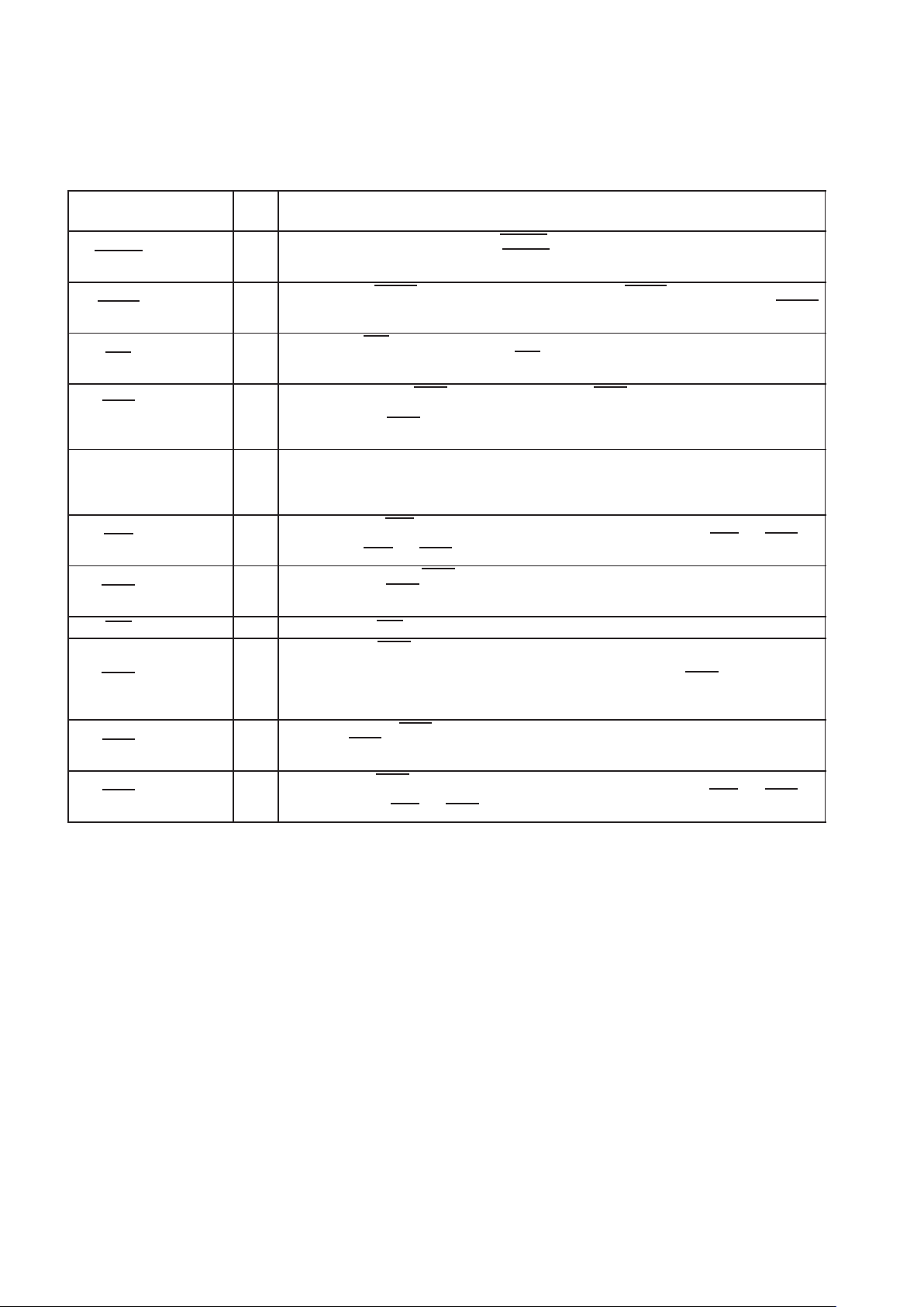
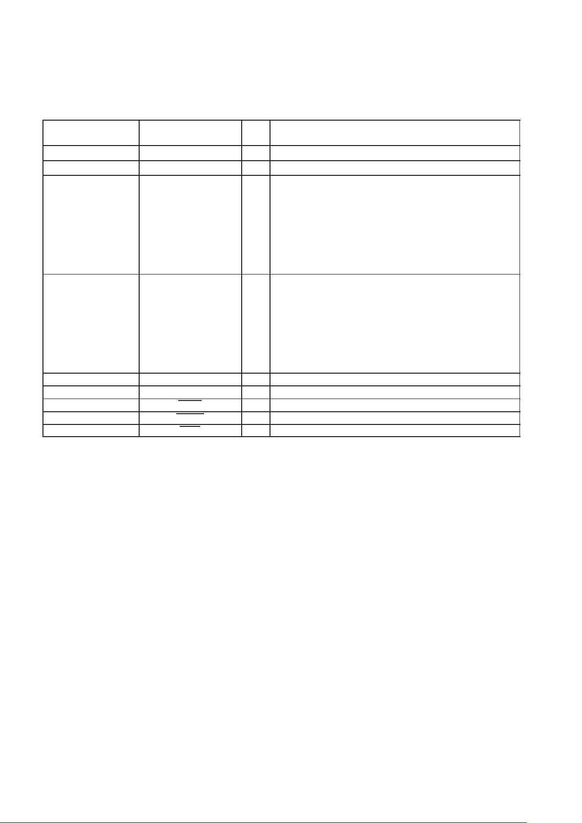
2 Terminal Descriptions
The PCI1451 is packaged in a 257-ball MicroStar BGA package.
1917
16
13141511
12
9
8 10
V
U
W
R
N
P
L
M
K
T
75
6
3
4
H
F
G
E
C
D
1
A
B
2
J
18
Figure 2–1. PCI1451 GJG Terminal Diagram
Table 2–1 shows the GJG terminal assignments for the CardBus and 16-bit PC Card signal names.
Table 2–2 shows the CardBus PC Card signal names sorted alphanumerically to the GJG terminal number.
Table 2–3 shows the 16-bit PC Card signal names sorted alphanumerically to the GJG terminal number.

2–2
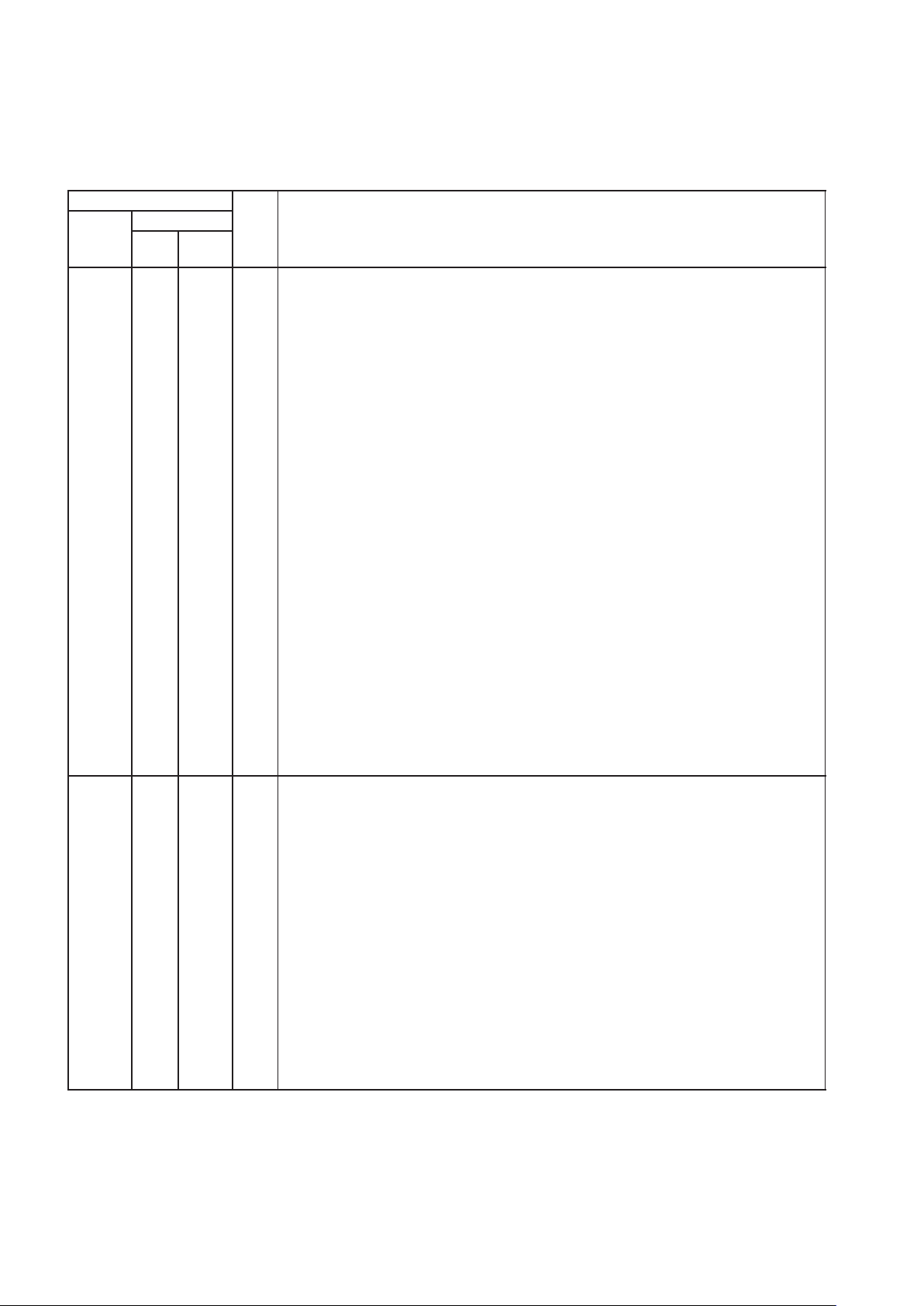
Table 2–1. GJG Terminals Sorted Alphanumerically for CardBus // 16-Bit Signals
TERM.
SIGNAL NAME
TERM.
SIGNAL NAME
TERM.
SIGNAL NAME
TERM
.
NO.
CARDBUS
16-BIT
TERM
.
NO.
CARDBUS
16-BIT
TERM
.
NO.
CARDBUS
16-BIT
A2 A_CC/BE1 A_ADDR8 D5 A_CAD13 A_IORD F14 B_CAD15 B_IOWR
A3 GND GND D6 A_CC/BE0 A_CE1 F15 B_CAD12 B_ADDR11
A4 A_CAD12 A_ADDR11 D7 A_CAD5 A_DATA6 F16 B_CAD13 B_IORD
A5 A_CAD10 A_CE2 D8 GND GND F18 V
CCB
V
CCB
A6 A_CAD8 A_DATA15 D9 B_RSVD B_DATA2 F19 B_CAD11 B_OE
A7 A_CAD3 A_DATA5 D10 B_CCD2 B_CD2 G1 GND GND
A8 A_CAD0 A_DATA3 D11 B_CAD26 B_ADDR0 G2 A_CAD18 A_ADDR7
A9 B_CAD29 B_DATA1 D12 B_CAD24 B_ADDR2 G4 A_CAD19 A_ADDR25
A10 B_CSTSCHG B_BVD1(STSCHG/RI) D13 B_CAD23 B_ADDR3 G5 A_CAD17 A_ADDR24
A11 V
CC
V
CC
D14 V
CC
V
CC
G6 A_CC/BE2 A_ADDR12
A12 B_CC/BE3 B_REG D15 B_CFRAME B_ADDR23 G7 A_CAD4 A_DATA12
A13 B_CREQ B_INPACK D16 B_CBLOCK B_ADDR19 G13 B_CAD7 B_DATA7
A14 B_CVS2 B_VS2 D18 B_RSVD B_ADDR18 G14 B_CAD10 B_CE2
A15 B_CAD17 B_ADDR24 D19 B_CC/BE1 B_ADDR8 G15 B_CAD9 B_ADDR10
A16 GND GND E1 V
CC
V
CC
G16 B_CC/BE0 B_CE1
A17 B_CCLK B_ADDR16 E2 A_CCLK A_ADDR16 G18 B_CAD8 B_DATA15
A18 B_CDEVSEL B_ADDR21 E4 A_CGNT A_WE G19 GND GND
B1 A_CPAR A_ADDR13 E5 A_CDEVSEL A_ADDR21 H1 A_CAD20 A_ADDR6
B2 A_RSVD A_ADDR18 E6 V
CC
V
CC
H2 A_CRST A_RESET
B3 A_CAD16 A_ADDR17 E7 A_RSVD A_DATA14 H4 A_CAD21 A_ADDR5
B4 A_CAD15 A_IOWR E8 A_CAD1 A_DATA4 H5 A_CAD22 A_ADDR4
B5 A_CAD11 A_OE E9 B_CAD31 B_DATA10 H6 A_CVS2 A_VS2
B6 V
CCA
V
CCA
E10 B_CAD27 B_DATA0 H14 B_CAD4 B_DATA12
B7 A_CAD6 A_DATA13 E11 B_CINT B_READY(IREQ) H15 B_RSVD B_DATA14
B8 A_CAD2 A_DATA11 E12 B_CAD25 B_ADDR1 H16 B_CAD5 B_DATA6
B9 B_CAD30 B_DATA9 E13 B_CAD21 B_ADDR5 H18 B_CAD6 B_DATA13
B10 B_CCLKRUN B_WP(IOIS16) E14 B_CAD19 B_ADDR25 H19 B_CAD3 B_DATA5
B11 B_CVS1 B_VS1 E15 B_CC/BE2 B_ADDR12 J1 A_CAD23 A_ADDR3
B12 V
CCB
V
CCB
E16 B_CAD16 B_ADDR17 J2 A_CC/BE3 A_REG
B13 B_CAD22 B_ADDR4 E18 B_CAD14 B_ADDR9 J4 A_CREQ A_INPACK
B14 B_CAD20 B_ADDR6 E19 V
CC
V
CC
J5 A_CAD24 A_ADDR2
B15 B_CAD18 B_ADDR7 F1 V
CCA
V
CCA
J6 A_CAD25 A_ADDR1
B16 B_CIRDY B_ADDR15 F2 A_CFRAME A_ADDR23 J14 V
CC
V
CC
B17 B_CTRDY B_ADDR22 F4 A_CIRDY A_ADDR15 J15 B_CAD1 B_DATA4
B18 B_CGNT B_WE F5 A_CTRDY A_ADDR22 J16 B_CAD2 B_DATA11
B19 B_CSTOP B_ADDR20 F6 A_CAD9 A_ADDR10 J18 B_CAD0 B_DATA3
C1 GND GND F7 A_CAD7 A_DATA7 J19 B_CCD1 B_CD1
C2 A_CBLOCK A_ADDR19 F8 A_CCD1 A_CD1 K1 A_CVS1 A_VS1
C18 B_CPERR B_ADDR14 F9 B_CAD28 B_DATA8 K2 A_CINT A_READY(IREQ)
C19 B_CPAR B_ADDR13 F10 B_CAUDIO B_BVD2(SPKR) K4 A_CSERR A_WAIT
D1 A_CPERR A_ADDR14 F11 B_CSERR B_WAIT K5 V
CCA
V
CCA
D2 A_CSTOP A_ADDR20 F12 GND GND K6 A_CAD26 A_ADDR0
D4 A_CAD14 A_ADDR9 F13 B_CRST B_RESET K14 GNT GNT

2–3
Table 2–1. GJG Terminals Sorted Alphanumerically for CardBus // 16-Bit Signals (continued)
TERM.
SIGNAL NAME
TERM.
SIGNAL NAME
TERM.
SIGNAL NAME
TERM
.
NO.
CARDBUS
16-BIT
TERM
.
NO.
CARDBUS
16-BIT
TERM
.
NO.
CARDBUS
16-BIT
K15 PCLK PCLK P9 MFUNC2 MFUNC2 T18 FRAME FRAME
K18 CLKRUN CLKRUN P10 MFUNC1 MFUNC1 T19 IRDY IRDY
K19 PRST PRST P11 GRST GRST U1 ZV_UV3 ZV_UV3
L1 A_CSTSCHG A_BVD1(STSCHG/RI) P12 IRQSER IRQSER U2 ZV_UV6 ZV_UV6
L2 A_CCLKRUN A_WP(IOIS16) P13 AD6 AD6 U18 TRDY TRDY
L4 A_CCD2 A_CD2 P14 AD9 AD9 U19 DEVSEL DEVSEL
L5 A_CAD27 A_DATA0 P15 V
CC
V
CC
V1 ZV_UV5 ZV_UV5
L6 A_CAUDIO A_BVD2(SPKR) P16 AD19 AD19 V2 ZV_SCLK ZV_SCLK
L14 REQ REQ P18 AD21 AD21 V3 ZV_LRCLK ZV_LRCLK
L15 AD31 AD31 P19 AD20 AD20 V4 ZV_PCLK ZV_PCLK
L16 AD28 AD28 R1 ZV_Y7 ZV_Y7 V5 RSVD RSVD
L18 AD30 AD30 R2 ZV_UV0 ZV_UV0 V6 RSVD RSVD
L19 AD29 AD29 R4 ZV_UV2 ZV_UV2 V7 RSVD RSVD
M1 A_CAD29 A_DATA1 R5 MFUNC6 MFUNC6 V8 RSVD RSVD
M2 GND GND R6 RSVD RSVD V9 SCL SCL
M4 A_CAD30 A_DATA9 R7 RSVD RSVD V10 V
CC
V
CC
M5 A_RSVD A_DATA2 R8 RSVD RSVD V11 DATA DATA
M6 A_CAD28 A_DATA8 R9 MFUNC3 MFUNC3 V12 AD0 AD0
M14 C/BE3 C/BE3 R10 SUSPEND SUSPEND V13 V
CC
V
CC
M15 AD27 AD27 R11 RI_OUT RI_OUT V14 GND GND
M16 AD26 AD26 R12 AD2 AD2 V15 AD11 AD11
M18 AD25 AD25 R13 AD5 AD5 V16 AD14 AD14
M19 AD24 AD24 R14 AD8 AD8 V17 PAR PAR
N1 ZV_HREF ZV_HREF R15 AD16 AD16 V18 PERR PERR
N2 ZV_VSYNC ZV_VSYNC R16 C/BE2 C/BE2 V19 STOP STOP
N4 ZV_Y0 ZV_Y0 R18 AD18 AD18 W2 ZV_UV7 ZV_UV7
N5 ZV_Y1 ZV_Y1 R19 AD17 AD17 W3 ZV_MCLK ZV_MCLK
N6 ZV_Y2 ZV_Y2 T1 ZV_UV1 ZV_UV1 W4 ZV_SDATA ZV_SDATA
N7 A_CAD31 A_DATA10 T2 ZV_UV4 ZV_UV4 W5 MFUNC5 MFUNC5
N13 AD3 AD3 T4 GND GND W6 RSVD RSVD
N14 AD22 AD22 T5 V
CC
V
CC
W7 RSVD RSVD
N15 AD23 AD23 T6 RSVD RSVD W8 RSVD RSVD
N16 GND GND T7 GND GND W9 SDA SDA
N18 V
CCP
V
CCP
T8 RSVD RSVD W10 MFUNC0 MFUNC0
N19 IDSEL/MFUNC7 IDSEL/MFUNC7 T9 MFUNC4 MFUNC4 W11 LATCH LATCH
P1 V
CC
V
CC
T10 SPKROUT SPKROUT W12 GND GND
P2 ZV_Y3 ZV_Y3 T11 CLOCK CLOCK W13 V
CCP
V
CCP
P4 ZV_Y4 ZV_Y4 T12 AD1 AD1 W14 AD7 AD7
P5 ZV_Y5 ZV_Y5 T13 AD4 AD4 W15 AD10 AD10
P6 ZV_Y6 ZV_Y6 T14 C/BE0 C/BE0 W16 AD13 AD13
P7 RSVD RSVD T15 AD12 AD12 W17 AD15 AD15
P8 RSVD RSVD T16 C/BE1 C/BE1 W18 SERR SERR

2–4
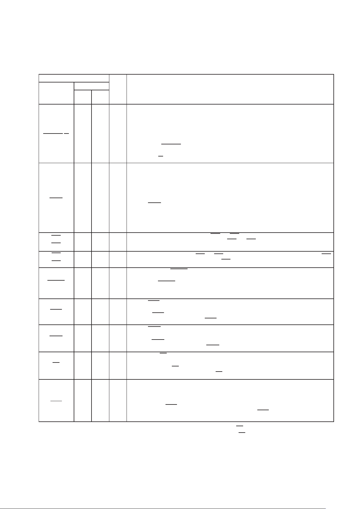
Table 2–2. CardBus PC Card Signal Names Sorted Alphanumerically to GJG Terminal Number
SIGNAL NAME
TERM.
NO.
SIGNAL NAME
TERM.
NO.
SIGNAL NAME
TERM.
NO.
SIGNAL NAME
TERM.
NO.
A_CAD0 A8 A_CFRAME F2 AD26 M16 B_CC/BE3 A12
A_CAD1 E8 A_CGNT E4 AD27 M15 B_CCD1 J19
A_CAD2 B8 A_CINT K2 AD28 L16 B_CCD2 D10
A_CAD3 A7 A_CIRDY F4 AD29 L19 B_CCLK A17
A_CAD4 G7 A_CPAR B1 AD30 L18 B_CCLKRUN B10
A_CAD5 D7 A_CPERR D1 AD31 L15 B_CDEVSEL A18
A_CAD6 B7 A_CREQ J4 B_CAD0 J18 B_CFRAME D15
A_CAD7 F7 A_CRST H2 B_CAD1 J15 B_CGNT B18
A_CAD8 A6 A_CSERR K4 B_CAD2 J16 B_CINT E11
A_CAD9 F6 A_CSTOP D2 B_CAD3 H19 B_CIRDY B16
A_CAD10 A5 A_CSTSCHG L1 B_CAD4 H14 B_CPAR C19
A_CAD11 B5 A_CTRDY F5 B_CAD5 H16 B_CPERR C18
A_CAD12 A4 A_CVS1 K1 B_CAD6 H18 B_CREQ A13
A_CAD13 D5 A_CVS2 H6 B_CAD7 G13 B_CRST F13
A_CAD14 D4 A_RSVD B2 B_CAD8 G18 B_CSERR F11
A_CAD15 B4 A_RSVD E7 B_CAD9 G15 B_CSTOP B19
A_CAD16 B3 A_RSVD M5 B_CAD10 G14 B_CSTSCHG A10
A_CAD17 G5 AD0 V12 B_CAD11 F19 B_CTRDY B17
A_CAD18 G2 AD1 T12 B_CAD12 F15 B_CVS1 B11
A_CAD19 G4 AD2 R12 B_CAD13 F16 B_CVS2 A14
A_CAD20 H1 AD3 N13 B_CAD14 E18 B_RSVD D9
A_CAD21 H4 AD4 T13 B_CAD15 F14 B_RSVD D18
A_CAD22 H5 AD5 R13 B_CAD16 E16 B_RSVD H15
A_CAD23 J1 AD6 P13 B_CAD17 A15 C/BE0 T14
A_CAD24 J5 AD7 W14 B_CAD18 B15 C/BE1 T16
A_CAD25 J6 AD8 R14 B_CAD19 E14 C/BE2 R16
A_CAD26 K6 AD9 P14 B_CAD20 B14 C/BE3 M14
A_CAD27 L5 AD10 W15 B_CAD21 E13 CLKRUN K18
A_CAD28 M6 AD11 V15 B_CAD22 B13 CLOCK T11
A_CAD29 M1 AD12 T15 B_CAD23 D13 DATA V11
A_CAD30 M4 AD13 W16 B_CAD24 D12 DEVSEL U19
A_CAD31 N7 AD14 V16 B_CAD25 E12 FRAME T18
A_CAUDIO L6 AD15 W17 B_CAD26 D11 GND A3
A_CBLOCK C2 AD16 R15 B_CAD27 E10 GND A16
A_CC/BE0 D6 AD17 R19 B_CAD28 F9 GND C1
A_CC/BE1 A2 AD18 R18 B_CAD29 A9 GND D8
A_CC/BE2 G6 AD19 P16 B_CAD30 B9 GND F12
A_CC/BE3 J2 AD20 P19 B_CAD31 E9 GND G1
A_CCD1 F8 AD21 P18 B_CAUDIO F10 GND G19
A_CCD2 L4 AD22 N14 B_CBLOCK D16 GND M2
A_CCLK E2 AD23 N15 B_CC/BE0 G16 GND N16
A_CCLKRUN L2 AD24 M19 B_CC/BE1 D19 GND T4
A_CDEVSEL E5 AD25 M18 B_CC/BE2 E15 GND T7

2–5
Table 2–2. CardBus PC Card Signal Names Sorted Alphanumerically to GJG Terminal Number
(continued)
SIGNAL NAME
TERM.
NO.
SIGNAL NAME
TERM.
NO.
SIGNAL NAME
TERM.
NO.
SIGNAL NAME
TERM.
NO.
GND V14 RSVD P7 V
CC
A11 ZV_PCLK V4
GND W12 RSVD P8 V
CC
D14 ZV_SCLK V2
GNT K14 RSVD R6 V
CC
E1 ZV_SDATA W4
GRST P11 RSVD R7 V
CC
E6 ZV_UV0 R2
IDSEL/MFUNC7 N19 RSVD R8 V
CC
E19 ZV_UV1 T1
IRDY T19 RSVD T6 V
CC
J14 ZV_UV2 R4
IRQSER P12 RSVD T8 V
CC
P1 ZV_UV3 U1
LATCH W11 RSVD V5 V
CC
P15 ZV_UV4 T2
MFUNC0 W10 RSVD V6 V
CC
T5 ZV_UV5 V1
MFUNC1 P10 RSVD V7 V
CC
V10 ZV_UV6 U2
MFUNC2 P9 RSVD V8 V
CC
V13 ZV_UV7 W2
MFUNC3 R9 RSVD W6 V
CCA
B6 ZV_VSYNC N2
MFUNC4 T9 RSVD W7 V
CCA
F1 ZV_Y0 N4
MFUNC5 W5 RSVD W8 V
CCA
K5 ZV_Y1 N5
MFUNC6 R5 SCL V9 V
CCB
B12 ZV_Y2 N6
PAR V17 SDA W9 V
CCB
F18 ZV_Y3 P2
PCLK K15 SERR W18 V
CCP
N18 ZV_Y4 P4
PERR V18 SPKROUT T10 V
CCP
W13 ZV_Y5 P5
PRST K19 STOP V19 ZV_HREF N1 ZV_Y6 P6
REQ L14 SUSPEND R10 ZV_LRCLK V3 ZV_Y7 R1
RI_OUT R11 TRDY U18 ZV_MCLK W3

2–6
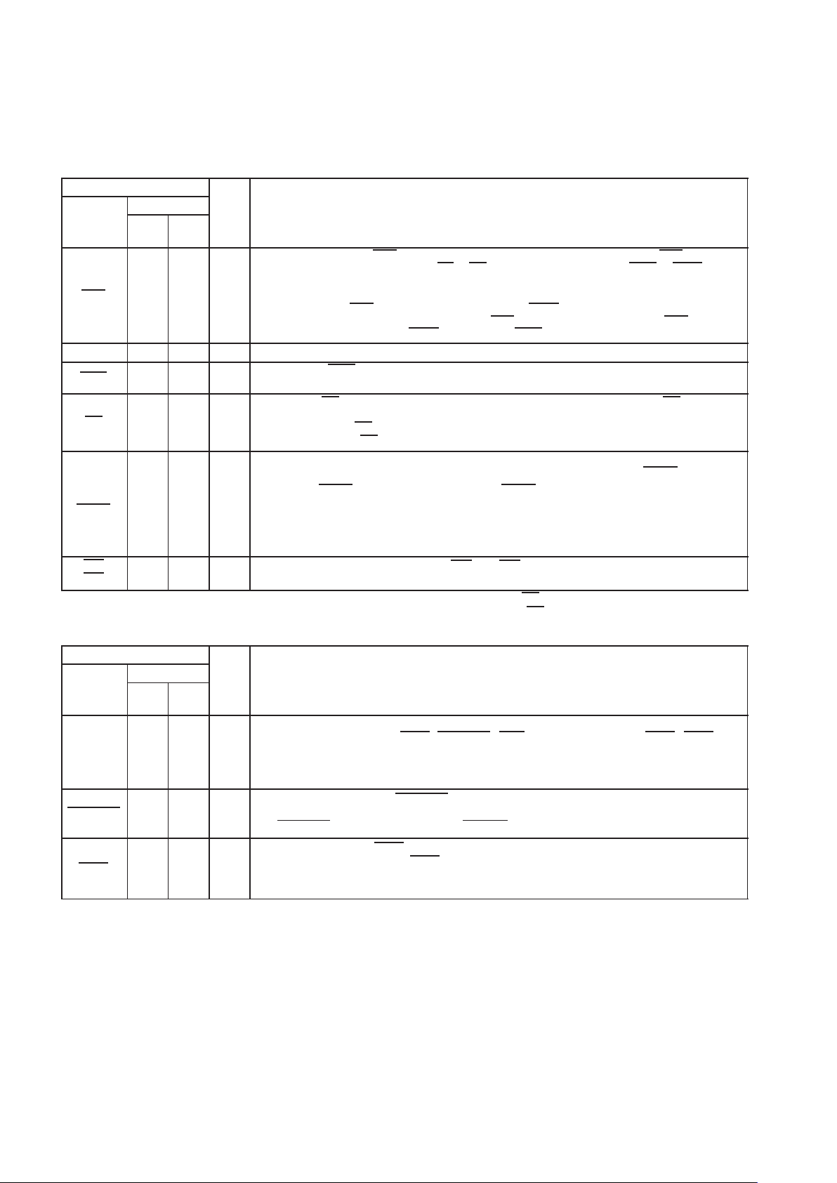
Table 2–3. 16-Bit PC Card Signal Names Sorted Alphanumerically to GJG Terminal Number
SIGNAL NAME
TERM.
NO.
SIGNAL NAME
TERM.
NO.
SIGNAL NAME
TERM.
NO.
SIGNAL NAME
TERM.
NO.
A_ADDR0 K6 A_DATA11 B8 AD26 M16 B_DATA5 H19
A_ADDR1 J6 A_DATA12 G7 AD27 M15 B_DATA6 H16
A_ADDR2 J5 A_DATA13 B7 AD28 L16 B_DATA7 G13
A_ADDR3 J1 A_DATA14 E7 AD29 L19 B_DATA8 F9
A_ADDR4 H5 A_DATA15 A6 AD30 L18 B_DATA9 B9
A_ADDR5 H4 A_INPACK J4 AD31 L15 B_DATA10 E9
A_ADDR6 H1 A_IORD D5 B_ADDR0 D11 B_DATA11 J16
A_ADDR7 G2 A_IOWR B4 B_ADDR1 E12 B_DATA12 H14
A_ADDR8 A2 A_OE B5 B_ADDR2 D12 B_DATA13 H18
A_ADDR9 D4 A_READY(IREQ) K2 B_ADDR3 D13 B_DATA14 H15
A_ADDR10 F6 A_REG J2 B_ADDR4 B13 B_DATA15 G18
A_ADDR11 A4 A_RESET H2 B_ADDR5 E13 B_INPACK A13
A_ADDR12 G6 A_VS1 K1 B_ADDR6 B14 B_IORD F16
A_ADDR13 B1 A_VS2 H6 B_ADDR7 B15 B_IOWR F14
A_ADDR14 D1 A_WAIT K4 B_ADDR8 D19 B_OE F19
A_ADDR15 F4 A_WE E4 B_ADDR9 E18 B_READY(IREQ) E11
A_ADDR16 E2 A_WP(IOIS16) L2 B_ADDR10 G15 B_REG A12
A_ADDR17 B3 AD0 V12 B_ADDR11 F15 B_RESET F13
A_ADDR18 B2 AD1 T12 B_ADDR12 E15 B_VS1 B11
A_ADDR19 C2 AD2 R12 B_ADDR13 C19 B_VS2 A14
A_ADDR20 D2 AD3 N13 B_ADDR14 C18 B_WAIT F11
A_ADDR21 E5 AD4 T13 B_ADDR15 B16 B_WE B18
A_ADDR22 F5 AD5 R13 B_ADDR16 A17 B_WP(IOIS16) B10
A_ADDR23 F2 AD6 P13 B_ADDR17 E16 C/BE0 T14
A_ADDR24 G5 AD7 W14 B_ADDR18 D18 C/BE1 T16
A_ADDR25 G4 AD8 R14 B_ADDR19 D16 C/BE2 R16
A_BVD1(STSCHG/RI) L1 AD9 P14 B_ADDR20 B19 C/BE3 M14
A_BVD2(SPKR) L6 AD10 W15 B_ADDR21 A18 CLKRUN K18
A_CD1 F8 AD11 V15 B_ADDR22 B17 CLOCK T11
A_CD2 L4 AD12 T15 B_ADDR23 D15 DATA V11
A_CE1 D6 AD13 W16 B_ADDR24 A15 DEVSEL U19
A_CE2 A5 AD14 V16 B_ADDR25 E14 FRAME T18
A_DATA0 L5 AD15 W17 B_BVD1(STSCHG/RI) A10 GND A3
A_DATA1 M1 AD16 R15 B_BVD2(SPKR) F10 GND A16
A_DATA2 M5 AD17 R19 B_CD1 J19 GND C1
A_DATA3 A8 AD18 R18 B_CD2 D10 GND D8
A_DATA4 E8 AD19 P16 B_CE1 G16 GND F12
A_DATA5 A7 AD20 P19 B_CE2 G14 GND G1
A_DATA6 D7 AD21 P18 B_DATA0 E10 GND G19
A_DATA7 F7 AD22 N14 B_DATA1 A9 GND M2
A_DATA8 M6 AD23 N15 B_DATA2 D9 GND N16
A_DATA9 M4 AD24 M19 B_DATA3 J18 GND T4
A_DATA10 N7 AD25 M18 B_DATA4 J15 GND T7

2–7
Table 2–3. 16-Bit PC Card Signal Names Sorted Alphanumerically to GJG Terminal Number (continued)
SIGNAL NAME
TERM.
NO.
SIGNAL NAME
TERM.
NO.
SIGNAL NAME
TERM.
NO.
SIGNAL NAME
TERM.
NO.
GND V14 RSVD P7 V
CC
A11 ZV_PCLK V4
GND W12 RSVD P8 V
CC
D14 ZV_SCLK V2
GNT K14 RSVD R6 V
CC
E1 ZV_SDATA W4
GRST P11 RSVD R7 V
CC
E6 ZV_UV0 R2
IDSEL/MFUNC7 N19 RSVD R8 V
CC
E19 ZV_UV1 T1
IRDY T19 RSVD T6 V
CC
J14 ZV_UV2 R4
IRQSER P12 RSVD T8 V
CC
P1 ZV_UV3 U1
LATCH W11 RSVD V5 V
CC
P15 ZV_UV4 T2
MFUNC0 W10 RSVD V6 V
CC
T5 ZV_UV5 V1
MFUNC1 P10 RSVD V7 V
CC
V10 ZV_UV6 U2
MFUNC2 P9 RSVD V8 V
CC
V13 ZV_UV7 W2
MFUNC3 R9 RSVD W6 V
CCA
B6 ZV_VSYNC N2
MFUNC4 T9 RSVD W7 V
CCA
F1 ZV_Y0 N4
MFUNC5 W5 RSVD W8 V
CCA
K5 ZV_Y1 N5
MFUNC6 R5 SCL V9 V
CCB
B12 ZV_Y2 N6
PAR V17 SDA W9 V
CCB
F18 ZV_Y3 P2
PCLK K15 SERR W18 V
CCP
N18 ZV_Y4 P4
PERR V18 SPKROUT T10 V
CCP
W13 ZV_Y5 P5
PRST K19 STOP V19 ZV_HREF N1 ZV_Y6 P6
REQ L14 SUSPEND R10 ZV_LRCLK V3 ZV_Y7 R1
RI_OUT R11 TRDY U18 ZV_MCLK W3
2–8
The terminals are grouped in tables by functionality such as PCI system function, power supply function, etc., for quick
reference. The terminal numbers are also listed for convenient reference.
Table 2–4. Power Supply
TERMINAL
NAME NO.
FUNCTION
GND
A3, A16, C1, D8,
F12, G1, G19, M2,
N16, T4, T7, V14,
W12
Device ground terminals
V
CC
A11, D14, E1, E6,
E19, J14, P1, P15,
T5, V10, V13
Power supply terminal for core logic (3.3 Vdc)
V
CCA
B6, F1, K5 Clamp voltage for PC Card A interface. Indicates Card A signaling environment.
V
CCB
B12, F18 Clamp voltage for PC Card B interface. Indicates Card B signaling environment.
V
CCP
N18, W13 Clamp voltage for PCI signaling (3.3 Vdc or 5 Vdc)
T able 2–5. PC Card Power Switch
TERMINAL
NAME NO.
I/O FUNCTION
CLOCK T11 I/O
3-line power switch clock. Information on the DATA line is sampled at the rising edge of CLOCK. This
terminal defaults as an input which means an external clock source must be used. If the internal ring
oscillator is used, then an external CLOCK source is not required. The internal oscillator may be enabled
by setting bit 27 (P2CCLK) of the system control register (PCI offset 80h, see Section 4.29) to a 1b.
A 43-kW pulldown resistor should be tied to this terminal.
DATA V11 O
3-line power switch data. DATA is used to serially communicate socket power-control information to the
power switch.
LATCH W11 O
3-line power switch latch. LATCH is asserted by the PCI4450 to indicate to the PC Card power switch that
the data on the DATA line is valid.
Table 2–6. PCI System
TERMINAL
NAME NO.
I/O
FUNCTION
CLKRUN
K18 I/O
PCI clock run. CLKRUN is used by the central resource to request permission to stop the PCI clock or to
slow it down, and the PCI4450 responds accordingly. If CLKRUN
is not implemented, then this termomal
should be tied low. CLKRUN
is enabled by default by bit 1 (KEEPCLK) in the system control register (PCI
offset 80h, see Section 4.29).
PCLK K15 I
PCI bus clock. PCLK provides timing for all transactions on the PCI bus. All PCI signals are sampled at
the rising edge of PCLK.
PRST
K19 I
PCI bus reset. When the PCI bus reset is asserted, PRST causes the PCI4450 to place all output buffers
in a high-impedance state and reset all internal registers. When PRST
is asserted, the device is completely
nonfunctional. After PRST
is deasserted, the PCI4450 is in its default state. When the SUSPEND mode
is enabled, the device is protected from the PRST
and the internal registers are preserved. All outputs are
placed in a high-impedance state, but the contents of the registers are preserved.
GRST P11 I
Global reset. When the global reset is asserted, the GRST signal causes the PCI4450 to place all output
buffers in a high-impedance state and reset all internal registers. When GRST
is asserted, the device is
completely in its default state. For systems that require wake-up from D3, GRST
will normally be asserted
only during initial boot. PRST
should be asserted following initial boot so that PME context is retained when
transitioning from D3 to D0. For systems that do not require wake-up from D3, GRST
should be tied to
PRST
.
2–9
Table 2–7. PCI Address and Data
TERMINAL
NAME NO.
I/O
FUNCTION
AD31
AD30
AD29
AD28
AD27
AD26
AD25
AD24
AD23
AD22
AD21
AD20
AD19
AD18
AD17
AD16
AD15
AD14
AD13
AD12
AD11
AD10
AD9
AD8
AD7
AD6
AD5
AD4
AD3
AD2
AD1
AD0
L15
L18
L19
L16
M15
M16
M18
M19
N15
N14
P18
P19
P16
R18
R19
R15
W17
V16
W16
T15
V15
W15
P14
R14
W14
P13
R13
T13
N13
R12
T12
V12
I/O
PCI address/data bus. These signals make up the multiplexed PCI address and data bus on the primary interface.
During the address phase of a primary bus PCI cycle, AD31–AD0 contain a 32-bit address or other destination
information. During the data phase, AD31–AD0 contain data.
C/BE3
C/BE2
C/BE1
C/BE0
M14
R16
T16
T14
I/O
PCI bus commands and byte enables. These signals are multiplexed on the same PCI terminals. During the
address phase of a primary bus PCI cycle, C/BE3
–C/BE0 define the bus command. During the data phase, this
4-bit bus is used as byte enables. The byte enables determine which byte paths of the full 32-bit data bus carry
meaningful data. C/BE0
applies to byte 0 (AD7–AD0), C/BE1 applies to byte 1 (AD15–AD8), C/BE2 applies to
byte 2 (AD23–AD16), and C/BE3
applies to byte 3 (AD31–AD24).
PAR V17 I/O
PCI bus parity. In all PCI bus read and write cycles, the PCI4450 calculates even parity across the AD31–AD0
and C/BE3
–C/BE0 buses. As an initiator during PCI cycles, the PCI4450 outputs this parity indicator with a
one-PCLK delay. As a target during PCI cycles, the calculated parity is compared to the initiator’s parity indicator .
A compare error results in the assertion of a parity error (PERR
).
2–10
Table 2–8. PCI Interface Control
TERMINAL
NAME NO.
I/O
FUNCTION
DEVSEL
U19 I/O
PCI device select. The PCI4450 asserts DEVSEL to claim a PCI cycle as the target device. As a PCI
initiator on the bus, the PCI4450 monitors DEVSEL
until a target responds. If no target responds before
timeout occurs, then the PCI4450 terminates the cycle with an initiator abort.
FRAME
T18 I/O
PCI cycle frame. FRAME is driven by the initiator of a bus cycle. FRAME is asserted to indicate that a
bus transaction is beginning, and data transfers continue while this signal is asserted. When FRAME
is deasserted, the PCI bus transaction is in the final data phase.
GNT
K14 I
PCI bus grant. GNT is driven by the PCI bus arbiter to grant the PCI4450 access to the PCI bus after
the current data transaction has completed. GNT
may or may not follow a PCI bus request, depending
on the PCI bus parking algorithm.
LOCK
(MFUNC7)
N19 I/O
PCI bus lock. MFUNC7/LOCK can be configured as PCI LOCK and used to gain exclusive access
downstream. Since this functionality is not typically used, other functions may be accessed through this
terminal. MFUNC7/LOCK
defaults to and can be configured through the multifunction routing status
register (PCI offset 8Ch, see Section 4.36).
IDSEL/MFUNC7 N19 I
Initialization device select. IDSEL selects the PCI4450 during configuration space accesses. IDSEL can
be connected to one of the upper 24 PCI address lines on the PCI bus. If the LATCH terminal (W12/W11)
has an external pulldown resistor, then this terminal is configurable as MFUNC7 and IDSEL defaults to
the AD23 terminal.
IRDY
T19 I/O
PCI initiator ready. IRDY indicates the PCI bus initiator’s ability to complete the current data phase of
the transaction. A data phase is completed on a rising edge of PCLK where both IRDY
and TRDY are
asserted. Until IRDY
and TRDY are both sampled asserted, wait states are inserted.
PERR
V18 I/O
PCI parity error indicator. PERR is driven by a PCI device to indicate that calculated parity does not
match PAR when PERR
is enabled through bit 6 of the command register (PCI offset 04h, see
Section 4.4).
REQ
L14 O PCI bus request. REQ is asserted by the PCI4450 to request access to the PCI bus as an initiator.
SERR
W18 O
PCI system error. SERR is an output that is pulsed from the PCI4450 when enabled through bit 8 of the
command register (PCI offset 04h, see Section 4.4), indicating a system error has occurred. The
PCI4450 need not be the target of the PCI cycle to assert this signal. When SERR
is enabled by bit 1
in the bridge control register (PCI offset 3Eh, see Section 4.25), this signal also pulses, indicating that
an address parity error has occurred on a CardBus interface.
STOP
V19 I/O
PCI cycle stop signal. STOP is driven by a PCI target to request the initiator to stop the current PCI bus
transaction. STOP
is used for target disconnects and is commonly asserted by target devices that do
not support burst data transfers.
TRDY
U18 I/O
PCI target ready. TRDY indicates the primary bus target’s ability to complete the current data phase of
the transaction. A data phase is completed on a rising edge of PCLK when both IRDY
and TRDY are
asserted. Until both IRDY
and TRDY are asserted, wait states are inserted.
2–11
Table 2–9. System Interrupt
TERMINAL
NAME NO.
I/O
FUNCTION
INTA
(MFUNC0)
W10 I/O
Parallel PCI interrupt. INT A can be mapped to MFUNC0 when parallel PCI interrupts are used.
See Section 3.5,
Programmable Interrupt Subsystem
, for details on interrupt signaling. MFUNC0/INTA
defaults to a general-purpose input.
INTB
(MFUNC1)
P10 I/O
Parallel PCI interrupt. INTB can be mapped to MFUNC1 when parallel PCI interrupts are used.
See Section 3.5,
Programmable Interrupt Subsystem
, for details on interrupt signaling. MFUNC1/INTB
defaults to a general-purpose input.
IRQSER P12 I/O
Serial interrupt signal. IRQSER provides the IRQSER-style serial interrupting scheme. Serialized PCI
interrupts can also be sent in the IRQSER stream. See Section 3.5,
Programmable Interrupt Subsystem
,
for details on interrupt signaling.
MFUNC6 R5
MFUNC5 W5
Interrupt request/secondary functions multiplexed. The primary function of these terminals is to provide
MFUNC4 T9
Interru t request/secondary functions multi lexed. The rimary function of these terminals is to rovide
programmable options supported by the PCI4450. These interrupt multiplexer outputs can be mapped to
MFUNC4 T9
gy
various functions. See Section 4.36,
Multifunction Routing Status Register
, for options.
MFUNC3 R9
O
All of these terminals have secondary functions, such as PCI interrupts, PC/PCI DMA, GPE request/grant,
p
pp
p
p
MFUNC3 R9
O
ring indicate output, and zoomed video status, that can be selected w
ith th
e appropriate programming o
f
this register. When the secondary functions are enabled, the respective terminals are not available for
MFUNC2 P9
this register. When the secondary functions are enabled, the res ective terminals are not available for
multifunction routing.
MFUNC1 P10
See Section 4.36,
Multifunction Routing Status Register,
for programming options.
MFUNC0 W10
RI_OUT/PME R11 O
Ring indicate out and power management event output. Terminal provides an output to the system for
ring-indicate or PME
signals. Alternately, RI_OUT can be routed on MFUNC7.
Table 2–10. PC/PCI DMA
TERMINAL
NAME NO.
I/O
FUNCTION
PCGNT
(MFUNC2)
P9
PC/PCI DMA grant. PCGNT is used to grant the DMA channel to a requester in a system supporting the
PCGNT
(MFUNC3)
R9
I/O
PC/PCI DMA scheme. PCGNT, is available on MFUNC2 or MFUNC3.
This terminal is also used for the serial EEPROM interface.
PCREQ
(MFUNC7)
N19
PCREQ
(MFUNC4)
T9
O
PC/PCI DMA request. PCREQ is used to request DMA transfers as DREQ in a system supporting the
PC/PCI DMA scheme. PCREQ
is available on MFUNC7, MFUNC4, or MFUNC0.
PCREQ
(MFUNC0)
W10
Thi
s terminal is also used for the serial
EEPROM i
nterface.
2–12
Table 2–11. Zoomed Video
TERMINAL
I/O AND MEMORY
NAME NO.
I/O AND MEMORY
INTERFACE SIGNAL
I/O FUNCTION
ZV_HREF
N1 A10 O
Horizontal sync to the zoomed video port
ZV_VSYNC
N2 A11 O
Vertical sync to the zoomed video port
ZV_Y7
ZV_Y6
ZV_Y5
ZV_Y4
ZV_Y3
ZV_Y2
ZV_Y1
ZV_Y0
R1
P6
P5
P4
P2
N6
N5
N4
A20
A14
A19
A13
A18
A8
A17
A9
O Video data to the zoomed video port in YV:4:2:2 format
ZV_UV7
ZV_UV6
ZV_UV5
ZV_UV4
ZV_UV3
ZV_UV2
ZV_UV1
ZV_UV0
W2
U2
V1
T2
U1
R4
T1
R2
A25
A12
A24
A15
A23
A16
A22
A21
O Video data to the zoomed video port in YV:4:2:2 format
ZV_SCLK V2 A7 O Audio SCLK PCM
ZV_MCLK W3 A6 O Audio MCLK PCM
ZV_PCLK V4 IOIS16 O Pixel clock to the zoomed video port
ZV_LRCLK V3 INPACK O Audio LRCLK PCM
ZV_SDATA W4 SPKR O Audio SDATA PCM

2–13
Table 2–12. Miscellaneous
TERMINAL
NAME NO.
I/O
FUNCTION
MFUNC0 W10 I/O
Multifunction terminal 0. Defaults as a general-purpose input (GPI0), and can be programmed to perform
various functions. See Section 4.36,
Multifunction Routing Status Register,
for configuration details.
MFUNC1 P10 I/O
Multifunction terminal 1. Defaults as a general-purpose input (GPI1), and can be programmed to perform
various functions. See Section 4.36,
Multifunction Routing Status Register,
for configuration details.
MFUNC2
P9 I/O
Multifunction terminal 2. Defaults as a general-purpose input (GPI2), and can be programmed to perform
various functions. See Section 4.36,
Multifunction Routing Status Register,
for configuration details.
MFUNC3
R9 I/O
Multifunction terminal 3. Defaults as a general-purpose input (GPI3), and can be programmed to perform
various functions. See Section 4.36,
Multifunction Routing Status Register,
for configuration details.
MFUNC4
T9 I/O
Multifunction terminal 4. Defaults as a high–impedance reserved input, and can be programmed to
perform various functions. See Section 4.36,
Multifunction Routing Status Register,
for configuration
details.
MFUNC5
W5 I/O
Multifunction terminal 5. Defaults as a high-impedance reserved input, and can be programmed to
perform various functions. See Section 4.36,
Multifunction Routing Status Register,
for configuration
details.
MFUNC6 R5 I/O
Multifunction terminal 6. Defaults as a high-impedance reserved input, and can be programmed to
perform various functions. See Section 4.36,
Multifunction Routing Status Register,
for configuration
details.
IDSEL/MFUNC7 N19 I/O
IDSEL and multifunction terminal 7. Defaults as IDSEL, but may be used as a multifunction terminal. See
Section 4.36,
Multifunction Routing Status Register
and Section 3.4,
PC Card Applications Overview
, for
configuration details.
SCL V9 I/O
Serial ROM clock. This terminal provides the SCL serial clock signaling in a two-wire serial ROM
implementation, and is sensed at reset for serial ROM detection.
SDA W9 I/O
Serial ROM data. This terminal provides the SDA serial data signaling in a two-wire serial ROM
implementation.
SPKROUT
T10 O
Speaker output. SPKROUT is the output to the host system that can carry SPKR or CAUDIO through the
PCI4450 from the PC Card interface. SPKROUT is driven as the XOR combination of card
SPKR
//CAUDIO inputs.
SUSPEND
R10 I
Suspend. SUSPEND is used to protect the internal registers from clearing when PRST is asserted. See
Section 3.6.7,
Suspend Mode
for details.
2–14
Table 2–13. 16-Bit PC Card Address and Data (slots A and B)
TERMINAL
NO.
NAME
SLOT
A
†
SLOT
B
‡
I/O
FUNCTION
A25
A24
A23
A22
A21
A20
A19
A18
A17
A16
A15
A14
A13
A12
A11
A10
A9
A8
A7
A6
A5
A4
A3
A2
A1
A0
G4
G5
F2
F5
E5
D2
C2
B2
B3
E2
F4
D1
B1
G6
A4
F6
D4
A2
G2
H1
H4
H5
J1
J5
J6
K6
E14
A15
D15
B17
A18
B19
D16
D18
E16
A17
B16
C18
C19
E15
F15
G15
E18
D19
B15
B14
E13
B13
D13
D12
E12
D11
O PC Card address. 16-bit PC Card address lines. A25 is the most significant bit.
D15
D14
D13
D12
D11
D10
D9
D8
D7
D6
D5
D4
D3
D2
D1
D0
A6
E7
B7
G7
B8
N7
M4
M6
F7
D7
A7
E8
A8
M5
M1
L5
G18
H15
H18
H14
J16
E9
B9
F9
G13
H16
H19
J15
J18
D9
A9
E10
I/O PC Card data. 16-bit PC Card data lines. D15 is the most significant bit.
†
Terminal name for slot A is preceded with A_. For example, the full name for terminal G2 is A_ADDR25.
‡
Terminal name for slot B is preceded with B_. For example, the full name for terminal A16 is B_ADDR25.
2–15
Table 2–14. 16-Bit PC Card Interface Control (slots A and B)
TERMINAL
NO.
NAME
SLOT
A
†
SLOT
B
‡
I/O
FUNCTION
BVD1
(STSCHG
/RI)
L1 A10 I
Battery voltage detect 1. BVD1 is generated by 16-bit memory PC Cards that include batteries. BVD1
and BVD2 indicate the condition of the batteries on a memory PC Card. Both BVD1 and BVD2 are
kept high when the battery is good. When BVD2 is low and BVD1 is high, the battery is weak and
should be replaced. When BVD1 is low, the battery is no longer serviceable and the data in the
memory PC Card is lost. See Section 5.6,
ExCA Card Status-Change Interrupt Configuration
Register
, for the enable bits. See Section 5.5,
ExCA Card Status-Change Register
and Section 5.2,
ExCA Interface Status Register
, for the status bits for this signal.
Status change. STSCHG
is used to alert the system to a change in the READY, write protect, or
battery voltage dead condition of a 16-bit I/O PC Card.
Ring indicate. RI
is used by 16-bit modem cards to indicate a ring detection.
BVD2
(SPKR
)
L6 F10 I
Battery voltage detect 2. BVD2 is generated by 16-bit memory PC Cards that include batteries. BVD2
and BVD1 indicate the condition of the batteries on a memory PC Card. Both BVD1 and BVD2 are
high when the battery is good. When BVD2 is low and BVD1 is high, the battery is weak and should
be replaced. When BVD1 is low, the battery is no longer serviceable and the data in the memory PC
Card is lost. See Section 5.6,
ExCA Card Status-Change Interrupt Configuration Register
, for the
enable bits. See Section 5.5,
ExCA Card Status-Change Register
and Section 5.2,
ExCA Interface
Status Register
, for the status bits for this signal.
Speaker. SPKR
is an optional binary audio signal available only when the card and socket have been
configured for the 16-bit I/O interface. The audio signals from cards A and B are combined by the
PCI4450 and are output on SPKROUT.
DMA request. BVD2 can be used as the DMA request signal during DMA operations to a 16-bit
PC Card that supports DMA. The PC Card asserts BVD2 to indicate a request for a DMA operation.
CD1
CD2
F8L4J19
D10
I
PC Card detect 1 and PC Card detect 2. CD1 and CD2 are internally connected to ground on the PC
Card. When a PC Card is inserted into a socket, CD1
and CD2 are pulled low. For signal status, see
Section 5.2,
ExCA Interface Status Register
.
CE1
CE2
D6A5G16
G14
O
Card enable 1 and card enable 2. CE1 and CE2 enable even- and odd-numbered address bytes. CE1
enables even-numbered address bytes, and CE2 enables odd-numbered address bytes.
INPACK J4 A13 I
Input acknowledge. INPACK is asserted by the PC Card when it can respond to an I/O read cycle
at the current address.
DMA request. INPACK
can be used as the DMA request signal during DMA operations from a 16-bit
PC Card that supports DMA. If used as a strobe, then the PC Card asserts this signal to indicate a
request for a DMA operation.
IORD
D5 F16 O
I/O read. IORD is asserted by the PCI4450 to enable 16-bit I/O PC Card data output during host I/O
read cycles.
DMA write. IORD
is used as the DMA write strobe during DMA operations from a 16-bit PC Card that
supports DMA. The PCI4450 asserts IORD
during DMA transfers from the PC Card to host memory.
IOWR
B4 F14 O
I/O write. IOWR is driven low by the PCI4450 to strobe write data into 16-bit I/O PC Cards during host
I/O write cycles.
DMA read. IOWR is used as the DMA write strobe during DMA operations from a 16-bit PC Card that
supports DMA. The PCI4450 asserts IOWR
during transfers from host memory to the PC Card.
OE B5 F19 O
Output enable. OE is driven low by the PCI4450 to enable 16-bit memory PC Card data output during
host memory read cycles.
DMA terminal count. OE is used as terminal count (TC) during DMA operations to a 16-bit PC Card
that supports DMA. The PCI4450 asserts OE to indicate TC for a DMA write operation.
READY
(IREQ
)
K2 E11 I
Ready. The ready function is provided by READY when the 16-bit PC Card and the host socket are
configured for the memory-only interface. READY is driven low by the 16-bit memory PC Cards to
indicate that the memory card circuits are busy processing a previous write command. READY is
driven high when the 16-bit memory PC Card is ready to accept a new data transfer command.
Interrupt request. IREQ
is asserted by a 16-bit I/O PC Card to indicate to the host that a device on
the 16-bit I/O PC Card requires service by the host software. IREQ
is high (deasserted) when no
interrupt is requested.
†
Terminal name for slot A is preceded with A_. For example, the full name for terminal B5 is A_OE.
‡
Terminal name for slot B is preceded with B_. For example, the full name for terminal F19 is B_OE
.
2–16
Table 2–14. 16-Bit PC Card Interface Control (slots A and B) (continued)
TERMINAL
NO.
NAME
SLOT
A
†
SLOT
B
‡
I/O
FUNCTION
REG
J2 A12 O
Attribute memory select. REG remains high for all common memory accesses. When REG is asserted,
access is limited to attribute memory (OE
or WE active) and to the I/O space (IORD or IOWR active).
Attribute memory is a separately accessed section of card memory and is generally used to record card
capacity and other configuration and attribute information.
DMA acknowledge. REG
is used as a DMA acknowledge (DACK) during DMA operations to a 16-bit PC
Card that supports DMA. The PCI4450 asserts REG
to indicate a DMA operation. REG is used in
conjunction with the DMA read (IOWR
) or DMA write (IORD) strobes to transfer data.
RESET H2 F13 O PC Card reset. RESET forces a hard reset to a 16-bit PC Card.
WAIT
K4 F11 I
Bus cycle wait. WAIT is driven by a 16-bit PC Card to delay the completion of (i.e., extend) the memory
or I/O cycle in progress.
WE E4 B18 O
Write enable. WE is used to strobe memory write data into 16-bit memory PC Cards. WE is also used
for memory PC Cards that employ programmable memory technologies.
DMA terminal count. WE
is used as TC during DMA operations to a 16-bit PC Card that supports DMA.
The PCI4450 asserts WE to indicate TC for a DMA read operation.
WP
(IOIS16
)
L2 B10 I
Write protect. WP applies to 16-bit memory PC Cards. WP reflects the status of the write-protect switch
on 16-bit memory PC Cards. For 16-bit I/O cards, WP is used for the 16-bit port (IOIS16) function.
I/O is 16 bits. IOIS16
applies to 16-bit I/O PC Cards. IOIS16 is asserted by the 16-bit PC Card when the
address on the bus corresponds to an address to which the 16-bit PC Card responds, and the I/O port
that is addressed is capable of 16-bit accesses.
DMA request. WP can be used as the DMA request signal during DMA operations to a 16-bit PC Card
that supports DMA. If used, the PC Card asserts WP to indicate a request for a DMA operation.
VS1
VS2
K1H6B11
A14
I/O
Voltage sense 1 and voltage sense 2. VS1 and VS2, when used in conjunction with each other,
determine the operating voltage of the 16-bit PC Card.
†
Terminal name for slot A is preceded with A_. For example, the full name for terminal C1 is A_WE.
‡
Terminal name for slot B is preceded with B_. For example, the full name for terminal A19 is B_WE
.
Table 2–15. CardBus PC Card Interface System (slots A and B)
TERMINAL
NO.
NAME
SLOT
A
†
SLOT
B
‡
I/O
FUNCTION
CCLK E2 A17 O
CardBus PC Card clock. CCLK provides synchronous timing for all transactions on the CardBus
interface. All signals except CRST
, CCLKRUN, CINT, CSTSCHG, CAUDIO, CCD2, CCD1, and
CVS2–CVS1 are sampled on the rising edge of CCLK, and all timing parameters are defined with the
rising edge of this signal. CCLK operates at the PCI bus clock frequency, but it can be stopped in the
low state or slowed down for power savings.
CCLKRUN
L2 B10 O
CardBus PC Card clock run. CCLKRUN is used by a CardBus PC Card to request an increase in the
CCLK frequency, and by the PCI4450 to indicate that the CCLK frequency is decreased. CardBus clock
run (CCLKRUN
) follows the PCI clock run (CLKRUN).
CRST
H2 F13 I/O
CardBus PC Card reset. CRST is used to bring CardBus PC Card-specific registers, sequencers, and
signals to a known state. When CRST
is asserted, all CardBus PC Card signals must be placed in a
high-impedance state, and the PCI4450 drives these signals to a valid logic level. Assertion can be
asynchronous to CCLK, but deassertion must be synchronous to CCLK.
†
Terminal name for slot A is preceded with A_. For example, the full name for terminal E3 is A_CCLK.
‡
Terminal name for slot B is preceded with B_. For example, the full name for terminal B17 is B_CCLK.
 Loading...