

MSP430G2955
MSP430G2855
MSP430G2755
www.ti.com
SLAS800 –MARCH 2013
MIXED SIGNAL MICROCONTROLLER
Check for Samples: MSP430G2955, MSP430G2855, MSP430G2755
1
FEATURES
• Low Supply-Voltage Range: 1.8 V to 3.6 V • Universal Serial Communication Interface
• Ultra-Low Power Consumption
– Active Mode: 250 µA at 1 MHz, 2.2 V
– Standby Mode: 0.7 µA
– Off Mode (RAM Retention): 0.1 µA
• Five Power-Saving Modes
• Ultra-Fast Wake-Up From Standby Mode in
Less Than 1 µs
• 16-Bit RISC Architecture, 62.5-ns Instruction
Cycle Time
• Basic Clock Module Configurations
– Internal Frequencies up to 16 MHz With
Four Calibrated Frequency
– Internal Very-Low-Power Low-Frequency
(LF) Oscillator
– 32-kHz Crystal
– High-Frequency (HF) Crystal up to 16 MHz
– External Digital Clock Source
– External Resistor
• Two 16-Bit Timer_A With Three
Capture/Compare Registers
• One 16-Bit Timer_B With Three
Capture/Compare Registers
• Up to 32 Touch-Sense-Enabled I/O Pins
(USCI)
– Enhanced UART Supporting Auto Baudrate
Detection (LIN)
– IrDA Encoder and Decoder
– Synchronous SPI
– I2C™
• On-Chip Comparator for Analog Signal
Compare Function or Slope Analog-to-Digital
(A/D) Conversion
• 10-Bit 200-ksps Analog-to-Digital (A/D)
Converter With Internal Reference, Sampleand-Hold, and Autoscan
• Brownout Detector
• Serial Onboard Programming,
No External Programming Voltage Needed,
Programmable Code Protection by Security
Fuse
• Bootstrap Loader
• On-Chip Emulation Logic
• Family Members are Summarized in Table 1
• Package Options
– TSSOP: 38 Pin (DA)
– QFN: 40 Pin (RHA)
• For Complete Module Descriptions, See the
MSP430x2xx Family User’s Guide (SLAU144)
DESCRIPTION
The Texas Instruments MSP430 family of ultra-low-power microcontrollers consists of several devices featuring
different sets of peripherals targeted for various applications. The architecture, combined with five low-power
modes, is optimized to achieve extended battery life in portable measurement applications. The device features a
powerful 16-bit RISC CPU, 16-bit registers, and constant generators that contribute to maximum code efficiency.
The digitally controlled oscillator (DCO) allows wake-up from low-power modes to active mode in less than 1 µs.
The MSP430G2x55 series are ultra-low-power mixed signal microcontrollers with built-in 16-bit timers, up to 32
I/O touch-sense-enabled pins, a versatile analog comparator, and built-in communication capability using the
universal serial communication interface. For configuration details, see Table 1.
Typical applications include low-cost sensor systems that capture analog signals, convert them to digital values,
and then process the data for display or for transmission to a host system.
1
Please be aware that an important notice concerning availability, standard warranty, and use in critical applications of
Texas Instruments semiconductor products and disclaimers thereto appears at the end of this data sheet.
PRODUCTION DATA information is current as of publication date.
Products conform to specifications per the terms of the Texas
Instruments standard warranty. Production processing does not
necessarily include testing of all parameters.
Copyright © 2013, Texas Instruments Incorporated
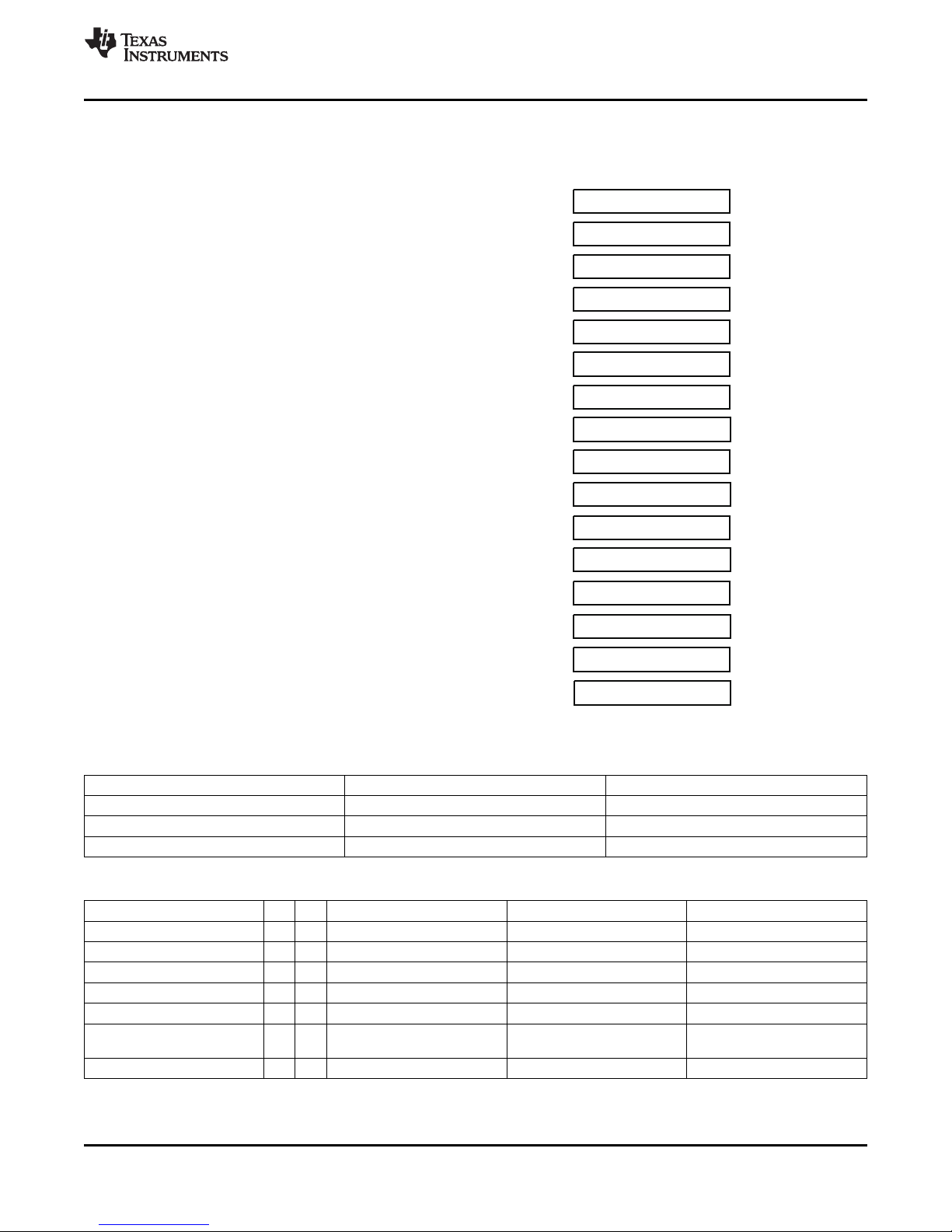
1TEST/SBWTCK
2DVCC
3P2.5/TA1.0/ROSC
4
XOUT/P2.7
5
XIN/P2.6 6
RST/NMI/SBWTDIO
7
P2.0/TA1CLK/ACLK/A0
8
P2.1/TA0INCLK/SMCLK/A1 9
P2.2/TA0.0/A2
10
P3.0/UCB0STE/UCA0CLK/A5
11
P3.1/UCB0SIMO/UCB0SDA 12
P3.2/UCB0SOMI/UCB0SCL
13
P3.3/UCB0CLK/UCA0STE
14
P4.0/TB 00. /CA0
15
P4.1/TB 10. /CA1
16
P4.2/TB 20. /CA2
17
P4.3/TB 0/A120. /CA3
18 P4.4/TB 1/A130. /CA4
19
38 P1.7/TA 2/TDO/TDI0.
37 P1.6/TA 1/TDI0.
36
P1.5/TA 0/TMS0.
35 P1.4/SMCLK/TCK
34
P1.3/TA 20.
33
P1.2/TA 10.
32 P1.1/TA 00.
31
P1.0/TA0CLK/ADC10CLK
30
P2.4/TA 2/A4/VREF+/VEREF+0.
29 P2.3/TA 1/A3/VREF−/VEREF−0.
28 P3.7/TA1.2/A7
27 P3.6/TA1.1/A6
26 P3.5/UCA0RXD/UCA0SOMI
25
P3.4/UCA0TXD/UCA0SIMO
24
23AVCC
22
AVSS
21
P4.7/TB0CLK/CA7
20
P4.6/TB0OUTH/A15/CA6
DVSS
P4.5/TB 2/A140. /CA5
MSP430G2955
MSP430G2855
MSP430G2755
SLAS800 –MARCH 2013
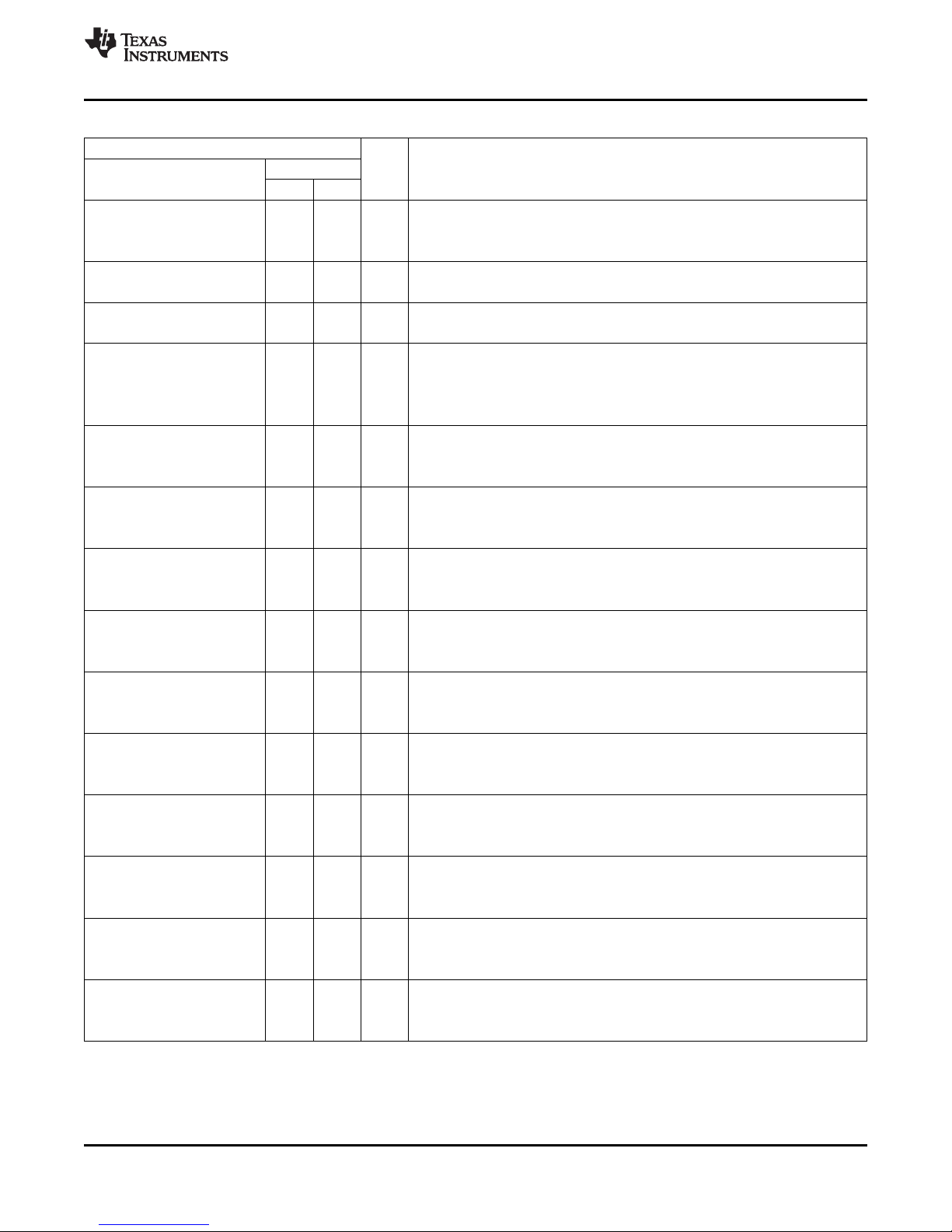
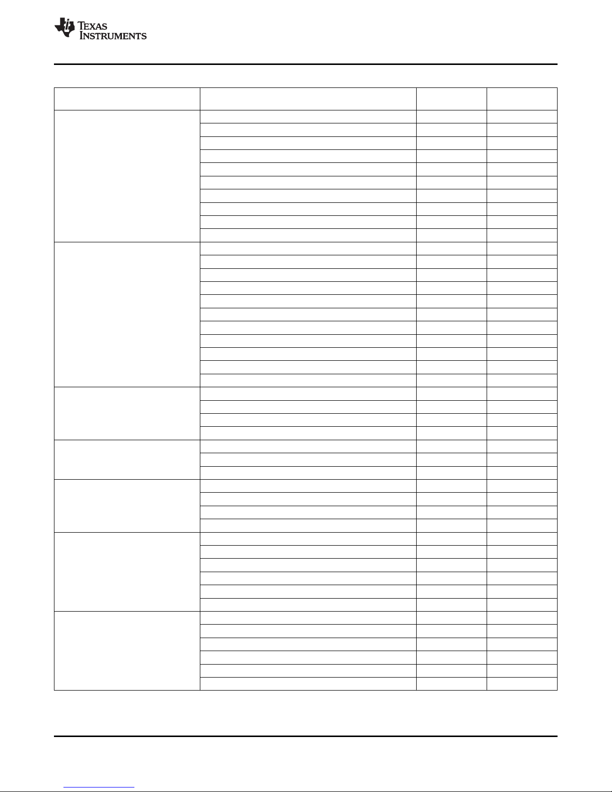
Table 1. Available Options
Device BSL EEM Clock I/O
MSP430G2955IDA38 HF, LF, 32 38-TSSOP
MSP430G2955IRHA40 32 40-QFN
MSP430G2855IDA38 HF, LF, 32 38-TSSOP
MSP430G2855IRHA40 32 40-QFN
MSP430G2755IDA38 HF, LF, 32 38-TSSOP
MSP430G2755IRHA40 32 40-QFN
1 1 56 4096 8 12 1 DCO,
1 1 48 4096 8 12 1 DCO,
1 1 32 4096 8 12 1 DCO,
Flash RAM Timer_A COMP_A+ ADC10 USCI_A0 Package
(KB) (B) Timer_B Channels Channels USCI_B0 Type
2x TA3
1x TB3
2x TA3
1x TB3
2x TA3
1x TB3
(1)(2)
VLO
VLO
VLO
(1) For the most current package and ordering information, see the Package Option Addendum at the end of this document, or see the TI
web site at www.ti.com.
(2) Package drawings, thermal data, and symbolization are available at www.ti.com/packaging.
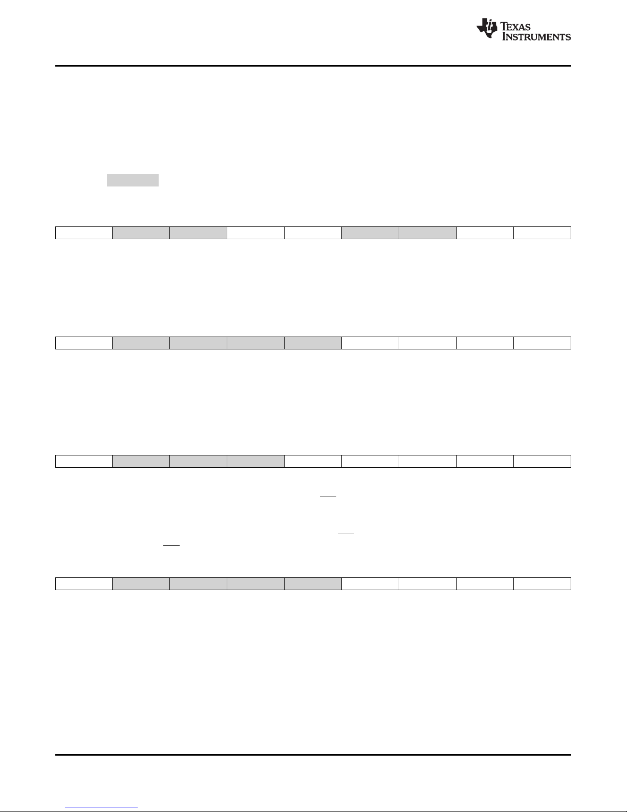
Device Pinout, 38-Pin TSSOP (DA Package)
www.ti.com
2 Submit Documentation Feedback Copyright © 2013, Texas Instruments Incorporated
Product Folder Links: MSP430G2955 MSP430G2855 MSP430G2755
Basic Clock
System+
RAM
Brownout
Protection
RST/NMI
VCC VSS
MCLK
SMCLK
Watchdog
WDT+
15 or 16 Bit
3 CC
Registers
16MHz
CPU
incl. 16
Registers
Emulation
(2BP)
XOUT
JTAG
Interface
Flash
56 kB
48 kB
32 kB
ACLK
XIN
MDB
MAB
Spy-Bi-Wire
3 CC
Registers,
Shadow
Register
USCI_A0:
UART, LIN,
IrDA,SPI
USCI_B0:
SPI,I2C
ADC
10-Bit
12
Channels,
Autoscan,
DTC
Ports P1, P2
2x8 I/O,
Interrupt
capability,
Pullup or
pulldown
resistors
P1.x, P2.x
2x8
P3.x, P4.x
2x8
4 kB
Timer0_A3
3 CC
Registers
Timer1_A3
Timer0_B3
COMP_A+
8
Channels
Ports P3, P4
2x8 I/O,
Pullup or
pulldown
resistors
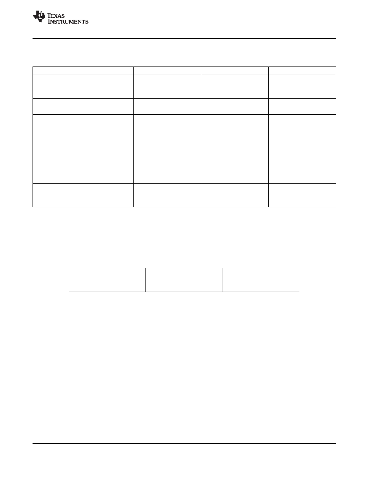
1DVSS
P1.5/TA0.0/TMS
P1.0/TA0CLK/ADC10CLK
P1.1/TA0.0
P1.2/TA0.1
P1.3/TA0.2
P1.4/SMCLK/TCK
13
P2.4/TA0.2/A4/VREF+/VEREF+
P2.5/TA1.0/ROSC
DVCC
TEST/SBWTCK
P1.6/TA0.1/TDI/TCLK
2
3
4
5
6
7
8
10
9
12 14 15 16 17 18 19
30
29
28
27
26
25
24
23
21
22
3839 37 36 35 34 33 32
XOUT/P2.7
XIN/P2.6
DVSS
RST/NMI/SBWTDIO
P2.0/TA1CLK/ACLK/A0
P2.1/TA0INCLK/SMCLK/A1
P2.2/TA0.0/A2
P3.0/UCB0STE/UCA0CLK/A5
P3.1/UCB0SIMO/UCB0SDA
DVCC
P1.7/TA0.2/TDO/TDI
P2.3/TA0.1/A3/VREF−/VEREF−
P3.7/TA1.2/A7
P3.6/TA1.1/A6
P3.5/UCA0RXD/UCA0SOMI
P3.4/UCA0TXD/UCA0SIMO
AVCC
AVSS
P3.3/UCB0CLK/UCA0STE
P4.0/TB0.0/CA0
P4.1/TB0.1/CA1
P4.2/TB0.2/CA2
P4.3/TB0.0/A12/CA3
P4.4/TB0.1/A13/CA4
P4.5/TB0.2/A14/CA5
P4.6/TB0OUTH/A15/CA6
P4.7/TB0CLK/CA7
www.ti.com
Device Pinout, 40-Pin QFN (RHA Package)
MSP430G2955
MSP430G2855
MSP430G2755
SLAS800 –MARCH 2013
Copyright © 2013, Texas Instruments Incorporated Submit Documentation Feedback 3
Product Folder Links: MSP430G2955 MSP430G2855 MSP430G2755
Functional Block Diagram
MSP430G2955
MSP430G2855
MSP430G2755
SLAS800 –MARCH 2013
Table 2. Terminal Functions
TERMINAL
NAME
P1.0/ General-purpose digital I/O pin
TACLK/ 31 29 I/O Timer_A, clock signal TACLK input
ADC10CLK ADC10, conversion clock
P1.1/ General-purpose digital I/O pin
TA0.0 Timer_A, capture: CCI0A input, compare: OUT0 output or BSL transmit
P1.2/ General-purpose digital I/O pin
TA0.1 Timer_A, capture: CCI1A input, compare: OUT1 output
P1.3/ General-purpose digital I/O pin
TA0.2 Timer_A, capture: CCI2A input, compare: OUT2 output
P1.4/ General-purpose digital I/O pin
SMCLK/ 35 33 I/O SMCLK signal output
TCK JTAG test clock, input terminal for device programming and test
P1.5/ General-purpose digital I/O pin
TA0.0/ 36 34 I/O Timer_A, compare: OUT0 output
TMS JTAG test mode select, input terminal for device programming and test
P1.6/ General-purpose digital I/O pin /
TA0.1/ Timer_A, compare: OUT1 output
TDI/ JTAG test data input terminal during programming and test
TCLK JTAG test clock input terminal during programming and test
P1.7/ General-purpose digital I/O pin
TA0.2/ Timer_A, compare: OUT2 output
TDO/ JTAG test data output terminal during programming and test
(1)
TDI
P2.0/ General-purpose digital I/O pin
TA1CLK/ Timer1_A3.TACLK
ACLK/ ACLK output
A0 ADC10, analog input A0
P2.1/ General-purpose digital I/O pin
TAINCLK/ Timer_A, clock signal at INCLK
SMCLK/ SMCLK signal output
A1 ADC10, analog input A1
P2.2/ General-purpose digital I/O pin
TA0.0/ 10 8 I/O Timer_A, capture: CCI0B input or BSL receive, compare: OUT0 output
A2 ADC10, analog input A2
P2.3/ General-purpose digital I/O pin
TA0.1/ Timer_A, capture CCI1B input, compare: OUT1 output
A3/ 29 27 I/O ADC10, analog input A3
VREF-/ Negative reference voltage output
VEREF- Negative reference voltage input
P2.4/ General-purpose digital I/O pin
TA0.2/ Timer_A, compare: OUT2 output
A4/ 30 28 I/O ADC10, analog input A4
VREF+/ Positive reference voltage output
VEREF+ Positive reference voltage input
NO. I/O DESCRIPTION
DA RHA
32 30 I/O
33 31 I/O
34 32 I/O
37 35 I/O
38 36 I/O
JTAG test data input terminal during programming and test
8 6 I/O
9 7 I/O
www.ti.com
(1) TDO or TDI is selected via JTAG instruction.
4 Submit Documentation Feedback Copyright © 2013, Texas Instruments Incorporated
Product Folder Links: MSP430G2955 MSP430G2855 MSP430G2755
MSP430G2955
MSP430G2855
MSP430G2755
www.ti.com
Table 2. Terminal Functions (continued)
TERMINAL
NAME
P2.5/ General-purpose digital I/O pin
TA1.0/ 3 40 I/O Timer_A, capture: CCI0B input or BSL receive, compare: OUT0 output
ROSC Input for external DCO resistor to define DCO frequency
XIN/ Input terminal of crystal oscillator
P2.6 General-purpose digital I/O pin
XOUT/ Output terminal of crystal oscillator
P2.7 General-purpose digital I/O pin
P3.0/ General-purpose digital I/O pin
UCB0STE/ USCI_B0 slave transmit enable
UCA0CLK/ USCI_A0 clock input/output
A5 ADC10, analog input A5
P3.1/ General-purpose digital I/O pin
UCB0SIMO/ 12 10 I/O USCI_B0 slave in, master out in SPI mode
UCB0SDA USCI_B0 SDA I2C data in I2C mode
P3.2/ General-purpose digital I/O pin
UCB0SOMI/ 13 11 I/O USCI_B0 slave out, master in SPI mode
UCB0SCL USCI_B0 SCL I2C clock in I2C mode
P3.3/ General-purpose digital I/O pin
UCB0CLK/ 14 12 I/O USCI_B0 clock input/output
UCA0STE USCI_A0 slave transmit enable
P3.4/ General-purpose digital I/O pin
UCA0TXD/ 25 23 I/O USCI_A0 transmit data output in UART mode
UCA0SIMO USCI_A0 slave in, master out in SPI mode
P3.5/ General-purpose digital I/O pin
UCA0RXD/ 26 24 I/O USCI_A0 receive data input in UART mode
UCA0SOMI USCI_A0 slave out, master in SPI mode
P3.6/ General-purpose digital I/O pin
TA1.1/ 27 25 I/O Timer_A, capture: CCI1B input or BSL receive, compare: OUT2 output
A6 ADC10 analog input A6
P3.7/ General-purpose digital I/O pin
TA1.2/ 28 26 I/O Timer_A, capture: CCI2B input or BSL receive, compare: OUT2 output
A7 ADC10 analog input A7
P4.0/ General-purpose digital I/O pin
TB0.0/ 17 15 I/O Timer_B, capture: CCI0A input, compare: OUT0 output
CA0 Comparator_A+, CA0 input
P4.1/ General-purpose digital I/O pin
TB0.1/ 18 16 I/O Timer_B, capture: CCI1A input, compare: OUT1 output
CA1 Comparator_A+, CA1 input
P4.2/ General-purpose digital I/O pin
TB0.2/ 19 17 I/O Timer_B, capture: CCI2A input, compare: OUT2 output
CA2 Comparator_A+, CA2 input
NO. I/O DESCRIPTION
DA RHA
6 3 I/O
5 2 I/O
11 9 I/O
(2)
SLAS800 –MARCH 2013
(2) If XOUT/P2.7 is used as an input, excess current flows until P2SEL.7 is cleared. This is due to the oscillator output driver connection to
this pad after reset.
Copyright © 2013, Texas Instruments Incorporated Submit Documentation Feedback 5
Product Folder Links: MSP430G2955 MSP430G2855 MSP430G2755

MSP430G2955
MSP430G2855
MSP430G2755
SLAS800 –MARCH 2013
Table 2. Terminal Functions (continued)
TERMINAL
NAME
P4.3/ General-purpose digital I/O pin
TB0.0/ Timer_B, capture: CCI0B input, compare: OUT0 output
A12/ ADC10 analog input A12
CA3 Comparator_A+, CA3 input
P4.4/ General-purpose digital I/O pin
TB0.1/ Timer_B, capture: CCI1B input, compare: OUT1 output
A13/ ADC10 analog input A13
CA4 Comparator_A+, CA4 input
P4.5/ General-purpose digital I/O pin
TB0.2/ Timer_B, compare: OUT2 output
A14/ ADC10 analog input A14
CA5 Comparator_A+, CA5 input
P4.6/ General-purpose digital I/O pin
TBOUTH/ Timer_B, switch all TB0 to TB3 outputs to high impedance
CAOUT/ 23 21 I/O Comparator_A+ Output
A15/ ADC10 analog input A15
CA6 Comparator_A+, CA6 input
P4.7/ General-purpose digital I/O pinCB0
TBCLK/ Timer_B, clock signal TBCLK input
CAOUT/ Comparator_A+ Output
CA7 Comparator_A+, CA7 input
RST/ Reset or nonmaskable interrupt input
NMI/SBWTDIO Spy-Bi-Wire test data input/output during programming and test
TEST/ Selects test mode for JTAG pins on Port 1. The device protection fuse is
SBWTCK Spy-Bi-Wire test clock input during programming and test
DV
CC
AV
CC
DV
SS
AV
SS
QFN Pad NA Pad NA QFN package pad; connection to DVSSrecommended.
NO. I/O DESCRIPTION
DA RHA
20 18 I/O
21 19 I/O
22 20 I/O
24 22 I/O
7 5 I
1 37 I
2 38, 39 Digital supply voltage
16 14 Analog supply voltage
4 1, 4 Digital ground reference
15 13 Analog ground reference
connected to TEST.
www.ti.com
6 Submit Documentation Feedback Copyright © 2013, Texas Instruments Incorporated
Product Folder Links: MSP430G2955 MSP430G2855 MSP430G2755
General-PurposeRegister
ProgramCounter
StackPointer
StatusRegister
ConstantGenerator
General-PurposeRegister
General-PurposeRegister
General-PurposeRegister
PC/R0
SP/R1
SR/CG1/R2
CG2/R3
R4
R5
R12
R13
General-PurposeRegister
General-PurposeRegister
R6
R7
General-PurposeRegister
General-PurposeRegister
R8
R9
General-PurposeRegister
General-PurposeRegister
R10
R11
General-PurposeRegister
General-PurposeRegister
R14
R15
www.ti.com
SHORT-FORM DESCRIPTION
CPU
The MSP430 CPU has a 16-bit RISC architecture
that is highly transparent to the application. All
operations, other than program-flow instructions, are
performed as register operations in conjunction with
seven addressing modes for source operand and four
addressing modes for destination operand.
The CPU is integrated with 16 registers that provide
reduced instruction execution time. The register-toregister operation execution time is one cycle of the
CPU clock.
Four of the registers, R0 to R3, are dedicated as
program counter, stack pointer, status register, and
constant generator, respectively. The remaining
registers are general-purpose registers.
Peripherals are connected to the CPU using data,
address, and control buses, and can be handled with
all instructions.
The instruction set consists of the original 51
instructions with three formats and seven address
modes and additional instructions for the expanded
address range. Each instruction can operate on word
and byte data.
MSP430G2955
MSP430G2855
MSP430G2755
SLAS800 –MARCH 2013
Instruction Set
The instruction set consists of 51 instructions with
three formats and seven address modes. Each
instruction can operate on word and byte data.
Table 3 shows examples of the three types of
instruction formats; Table 4 shows the address
modes.
Dual operands, source-destination ADD R4,R5 R4 + R5 ---> R5
Single operands, destination only CALL R8 PC -->(TOS), R8--> PC
Relative jump, un/conditional JNE Jump-on-equal bit = 0
Symbolic (PC relative) ✓ ✓ MOV EDE,TONI M(EDE) -- --> M(TONI)
Indirect autoincrement ✓ MOV @Rn+,Rm MOV @R10+,R11
(1) S = source, D = destination
INSTRUCTION FORMAT EXAMPLE OPERATION
ADDRESS MODE S D SYNTAX EXAMPLE OPERATION
Register ✓ ✓ MOV Rs,Rd MOV R10,R11 R10 -- --> R11
Indexed ✓ ✓ MOV X(Rn),Y(Rm) MOV 2(R5),6(R6) M(2+R5) -- --> M(6+R6)
Absolute ✓ ✓ MOV &MEM,&TCDAT M(MEM) -- --> M(TCDAT)
Indirect ✓ MOV @Rn,Y(Rm) MOV @R10,Tab(R6) M(R10) -- --> M(Tab+R6)
Immediate ✓ MOV #X,TONI MOV #45,TONI #45 -- --> M(TONI)
Table 3. Instruction Word Formats
Table 4. Address Mode Descriptions
(1)
M(R10) -- --> R11
R10 + 2-- --> R10
Copyright © 2013, Texas Instruments Incorporated Submit Documentation Feedback 7
Product Folder Links: MSP430G2955 MSP430G2855 MSP430G2755

MSP430G2955
MSP430G2855
MSP430G2755
SLAS800 –MARCH 2013
Operating Modes
The MSP430 has one active mode and five software selectable low-power modes of operation. An interrupt
event can wake up the device from any of the low-power modes, service the request, and restore back to the
low-power mode on return from the interrupt program.
The following six operating modes can be configured by software:
• Active mode (AM)
– All clocks are active.
• Low-power mode 0 (LPM0)
– CPU is disabled.
– ACLK and SMCLK remain active.
– MCLK is disabled.
• Low-power mode 1 (LPM1)
– CPU is disabled
– ACLK and SMCLK remain active.
– MCLK is disabled.
– DCO's dc generator is disabled if DCO not used in active mode.
• Low-power mode 2 (LPM2)
– CPU is disabled.
– ACLK remains active.
– MCLK and SMCLK are disabled.
– DCO's dc generator remains enabled.
• Low-power mode 3 (LPM3)
– CPU is disabled.
– ACLK remains active.
– MCLK and SMCLK are disabled.
– DCO's dc generator is disabled.
• Low-power mode 4 (LPM4)
– CPU is disabled.
– ACLK, MCLK, and SMCLK are disabled.
– DCO's dc generator is disabled.
– Crystal oscillator is stopped.
www.ti.com
8 Submit Documentation Feedback Copyright © 2013, Texas Instruments Incorporated
Product Folder Links: MSP430G2955 MSP430G2855 MSP430G2755

MSP430G2955
MSP430G2855
MSP430G2755
www.ti.com
Interrupt Vector Addresses
The interrupt vectors and the power-up starting address are located in the address range 0FFFFh to 0FFC0h.
The vector contains the 16-bit address of the appropriate interrupt handler instruction sequence.
If the reset vector (located at address 0FFFEh) contains 0FFFFh (for example, flash is not programmed), the
CPU goes into LPM4 immediately after power-up.
Table 5. Interrupt Sources, Flags, and Vectors
INTERRUPT SOURCE INTERRUPT FLAG PRIORITY
Power-Up PORIFG
External Reset RSTIFG
Watchdog Timer+ WDTIFG Reset 0FFFEh 31, highest
Flash key violation KEYV
PC out-of-range
(1)
(2)
NMI NMIIFG (non)-maskable
Oscillator fault OFIFG (non)-maskable 0FFFCh 30
Flash memory access violation ACCVIFG
Timer0_B3 TB0CCR0 CCIFG
Timer0_B3 TB0CCR2 TB0CCR1 CCIFG,
TBIFG
Comparator_A+ CAIFG
(2)(3)
(4)
(2)(4)
(4)
Watchdog Timer+ WDTIFG maskable 0FFF4h 26
Timer0_A3 TA0CCR0 CCIFG
Timer0_A3 TA0CCR2 TA0CCR1 CCIFG,
TAIFG
USCI_A0 or USCI_B0 receive UCA0RXIFG, UCB0RXIFG
(4)
(5)(4)
(2)(5)
USCI_B0 I2C status
USCI_A0 or USCI_B0 transmit UCA0TXIFG, UCB0TXIFG
(2)(6)
USCI_B0 I2C receive or transmit
ADC10 ADC10IFG
(4)
Reserved 0FFE8h 20
I/O Port P2 (up to eight flags) P2IFG.0 to P2IFG.7
I/O Port P1 (up to eight flags) P1IFG.0 to P1IFG.7
Timer1_A3 TA1CCR0 CCIFG
Timer1_A3 TA1CCR2 TA1CCR1 CCIFG,
TAIFG
(7)
See
(8)
See
(2)(4)
(2)(4)
(4)
(2)(4)
(1) A reset is generated if the CPU tries to fetch instructions from within the module register memory address range (0h to 01FFh) or from
within unused address ranges.
(2) Multiple source flags
(3) (non)-maskable: the individual interrupt-enable bit can disable an interrupt event, but the general interrupt enable cannot.
(4) Interrupt flags are located in the module.
(5) In SPI mode: UCB0RXIFG. In I2C mode: UCALIFG, UCNACKIFG, ICSTTIFG, UCSTPIFG.
(6) In UART or SPI mode: UCB0TXIFG. In I2C mode: UCB0RXIFG, UCB0TXIFG.
(7) This location is used as bootstrap loader security key (BSLSKEY). A 0xAA55 at this location disables the BSL completely. A zero (0h)
disables the erasure of the flash if an invalid password is supplied.
(8) The interrupt vectors at addresses 0FFDEh to 0FFC0h are not used in this device and can be used for regular program code if
necessary.
SYSTEM WORD
INTERRUPT ADDRESS
(non)-maskable
maskable 0FFFAh 29
maskable 0FFF8h 28
maskable 0FFF6h 27
maskable 0FFF2h 25
maskable 0FFF0h 24
maskable 0FFEEh 23
maskable 0FFECh 22
maskable 0FFEAh 21
maskable 0FFE6h 19
maskable 0FFE4h 18
maskable 0FFE2h 17
maskable 0FFE0h 16
0FFDEh 15
0FFDEh to
0FFC0h
SLAS800 –MARCH 2013
14 to 0, lowest
Copyright © 2013, Texas Instruments Incorporated Submit Documentation Feedback 9
Product Folder Links: MSP430G2955 MSP430G2855 MSP430G2755
MSP430G2955
MSP430G2855
MSP430G2755
SLAS800 –MARCH 2013
Special Function Registers (SFRs)
Most interrupt and module enable bits are collected into the lowest address space. Special function register bits
not allocated to a functional purpose are not physically present in the device. Simple software access is provided
with this arrangement.
Legend rw: Bit can be read and written.
rw-0,1: Bit can be read and written. It is reset or set by PUC.
rw-(0,1): Bit can be read and written. It is reset or set by POR.
SFR bit is not present in device.
Table 6. Interrupt Enable Register 1 and 2
Address 7 6 5 4 3 2 1 0
00h ACCVIE NMIIE OFIE WDTIE
rw-0 rw-0 rw-0 rw-0
WDTIE Watchdog timer interrupt enable. Inactive if watchdog mode is selected. Active if Watchdog timer is configured in
interval timer mode.
OFIE Oscillator fault interrupt enable
NMIIE (Non)maskable interrupt enable
ACCVIE Flash access violation interrupt enable
www.ti.com
Address 7 6 5 4 3 2 1 0
01h UCB0TXIE UCB0RXIE UCA0TXIE UCA0RXIE
rw-0 rw-0 rw-0 rw-0
UCA0RXIE USCI_A0 receive interrupt enable
UCA0TXIE USCI_A0 transmit interrupt enable
UCB0RXIE USCI_B0 receive interrupt enable
UCB0TXIE USCI_B0 transmit interrupt enable
Table 7. Interrupt Flag Register 1 and 2
Address 7 6 5 4 3 2 1 0
02h NMIIFG RSTIFG PORIFG OFIFG WDTIFG
rw-0 rw-(0) rw-(1) rw-1 rw-(0)
WDTIFG Set on watchdog timer overflow (in watchdog mode) or security key violation.
OFIFG Flag set on oscillator fault.
PORIFG Power-on reset interrupt flag. Set on VCCpower-up.
RSTIFG External reset interrupt flag. Set on a reset condition at RST/NMI pin in reset mode. Reset on VCCpower-up.
NMIIFG Set via RST/NMI pin
Address 7 6 5 4 3 2 1 0
03h UCB0TXIFG UCB0RXIFG UCA0TXIFG UCA0RXIFG
UCA0RXIFG USCI_A0 receive interrupt flag
UCA0TXIFG USCI_A0 transmit interrupt flag
UCB0RXIFG USCI_B0 receive interrupt flag
UCB0TXIFG USCI_B0 transmit interrupt flag
Reset on VCCpower-on or a reset condition at the RST/NMI pin in reset mode.
rw-1 rw-0 rw-1 rw-0
10 Submit Documentation Feedback Copyright © 2013, Texas Instruments Incorporated
Product Folder Links: MSP430G2955 MSP430G2855 MSP430G2755
MSP430G2955
MSP430G2855
MSP430G2755
www.ti.com
Memory Organization
Table 8. Memory Organization
MSP430G2755 MSP430G2855 MSP430G2955
Memory Size 32kB 48kB 56kB
Main: interrupt vector Flash 0xFFFF to 0xFFC0 0xFFFF to 0xFFC0 0xFFFF to 0xFFC0
Main: code memory Flash 0xFFFF to 0x8000 0xFFFF to 0x4000 0xFFFF to 0x2100
Information memory Size 256 Byte 256 Byte 256 Byte
Flash 0x10FF to 0x1000 0x10FF to 0x1000 0x10FF to 0x1000
RAM (total) Size 4kB 4kB 4kB
0x20FF to 0x1100 0x20FF to 0x1100 0x20FF to 0x1100
Extended Size 2KB 2KB 2KB
0x20FF to 0x1900 0x20FF to 0x1900 0x20FF to 0x1900
Mirrored Size 2KB 2KB 2KB
0x18FF to 0x1100 0x18FF to 0x1100 0x18FF to 0x1100
RAM (mirrored at 0x18FF to
0x1100)
Peripherals 16-bit 0x01FF to 0x0100 0x01FF to 0x0100 0x01FF to 0x0100
Size 2KB 2KB 2KB
0x09FF to 0x0200 0x09FF to 0x0200 0x09FF to 0x0200
8-bit 0x00FF to 0x0010 0x00FF to 0x0010 0x00FF to 0x0010
8-bit SFR 0x000F to 0x0000 0x000F to 0x0000 0x000F to 0x0000
SLAS800 –MARCH 2013
Bootstrap Loader (BSL)
The MSP430 BSL enables users to program the flash memory or RAM using a UART serial interface. Access to
the MSP430 memory via the BSL is protected by user-defined password. For complete description of the
features of the BSL and its implementation, see the MSP430 Programming Via the Bootstrap Loader User's
Guide (SLAU319).
Table 9. BSL Function Pins
BSL FUNCTION DA PACKAGE PINS RHA PACKAGE PINS
Data transmit 32 - P1.1 30 - P1.1
Data receive 10 - P2.2 8 - P2.2
Flash Memory
The flash memory can be programmed via the Spy-Bi-Wire or JTAG port or in-system by the CPU. The CPU can
perform single-byte and single-word writes to the flash memory. Features of the flash memory include:
• Flash memory has n segments of main memory and four segments of information memory (A to D) of
64 bytes each. Each segment in main memory is 512 bytes in size.
• Segments 0 to n may be erased in one step, or each segment may be individually erased.
• Segments A to D can be erased individually or as a group with segments 0 to n. Segments A to D are also
called information memory.
• Segment A contains calibration data. After reset segment A is protected against programming and erasing. It
can be unlocked but care should be taken not to erase this segment if the device-specific calibration data is
required.
Copyright © 2013, Texas Instruments Incorporated Submit Documentation Feedback 11
Product Folder Links: MSP430G2955 MSP430G2855 MSP430G2755

DCO(RSEL,DCO+1)
DCO(RSEL,DCO)
average
DCO(RSEL,DCO) DCO(RSEL,DCO+1)
32 × f × f
f =
MOD × f + (32 – MOD) × f
MSP430G2955
MSP430G2855
MSP430G2755
SLAS800 –MARCH 2013
Peripherals
Peripherals are connected to the CPU through data, address, and control buses and can be handled using all
instructions. For complete module descriptions, see the MSP430x2xx Family User's Guide (SLAU144).
Oscillator and System Clock
The clock system is supported by the basic clock module that includes support for a 32768-Hz watch crystal
oscillator, an internal very-low-power low-frequency oscillator and an internal digitally controlled oscillator (DCO).
The basic clock module is designed to meet the requirements of both low system cost and low power
consumption. The internal DCO provides a fast turn-on clock source and stabilizes in less than 1 µs. The basic
clock module provides the following clock signals:
• Auxiliary clock (ACLK), sourced either from a 32768-Hz watch crystal or the internal LF oscillator.
• Main clock (MCLK), the system clock used by the CPU.
• Sub-Main clock (SMCLK), the sub-system clock used by the peripheral modules.
The DCO settings to calibrate the DCO output frequency are stored in the information memory segment A.
Main DCO Characteristics
• All ranges selected by RSELx overlap with RSELx + 1: RSELx = 0 overlaps RSELx = 1, ... RSELx = 14
overlaps RSELx = 15.
• DCO control bits DCOx have a step size as defined by parameter S
• Modulation control bits MODx select how often f
cycles. The frequency f
DCO(RSEL,DCO)
is used for the remaining cycles. The frequency is an average equal to:
DCO(RSEL,DCO+1)
.
DCO
is used within the period of 32 DCOCLK
www.ti.com
12 Submit Documentation Feedback Copyright © 2013, Texas Instruments Incorporated
Product Folder Links: MSP430G2955 MSP430G2855 MSP430G2755
MSP430G2955
MSP430G2855
MSP430G2755
www.ti.com
Calibration Data Stored in Information Memory Segment A
Calibration data is stored for both the DCO and for ADC10 organized in a tag-length-value (TLV) structure.
Table 10. Tags Used by the Devices
NAME ADDRESS VALUE DESCRIPTION
TAG_DCO_30 0x10F6 0x01 DCO frequency calibration at VCC= 3 V and TA= 30°C at calibration
TAG_ADC10_1 0x10DA 0x10 ADC10_1 calibration tag
TAG_EMPTY - 0xFE Identifier for empty memory areas
Table 11. Labels Used by the Devices
LABEL SIZE CONDITION AT CALIBRATION AND DESCRIPTION
CAL_ADC_25T85 0x0010 word INCHx = 0x1010, REF2_5 = 1, TA= 85°C
CAL_ADC_25T30 0x000E word INCHx = 0x1010, REF2_5 = 1, TA= 30°C
CAL_ADC_25VREF_FACTOR 0x000C word REF2_5 = 1, TA= 30°C, I
CAL_ADC_15T85 0x000A word INCHx = 0x1010, REF2_5 = 0, TA= 85°C
CAL_ADC_15T30 0x0008 word INCHx = 0x1010, REF2_5 = 0, TA= 30°C
CAL_ADC_15VREF_FACTOR 0x0006 word REF2_5 = 0, TA= 30°C, I
CAL_ADC_OFFSET 0x0004 word External VREF = 1.5 V, f
CAL_ADC_GAIN_FACTOR 0x0002 word External VREF = 1.5 V, f
CAL_BC1_1MHZ 0x0009 byte -
CAL_DCO_1MHZ 0x0008 byte -
CAL_BC1_8MHZ 0x0007 byte -
CAL_DCO_8MHZ 0x0006 byte -
CAL_BC1_12MHZ 0x0005 byte -
CAL_DCO_12MHZ 0x0004 byte -
CAL_BC1_16MHZ 0x0003 byte -
CAL_DCO_16MHZ 0x0002 byte -
ADDRESS
OFFSET
VREF+
VREF+
ADC10CLK
ADC10CLK
= 1 mA
= 0.5 mA
= 5 MHz
= 5 MHz
SLAS800 –MARCH 2013
Brownout
The brownout circuit is implemented to provide the proper internal reset signal to the device during power on and
power off.
Digital I/O
Four 8-bit I/O ports are implemented:
• All individual I/O bits are independently programmable.
• Any combination of input, output, and interrupt condition (port P1 and port P2 only) is possible.
• Edge-selectable interrupt input capability for all bits of port P1 and port P2.
• Read and write access to port-control registers is supported by all instructions.
• Each I/O has an individually programmable pullup or pulldown resistor.
• Each I/O has an individually programmable pin oscillator enable bit to enable low-cost touch sensing.
Watchdog Timer (WDT+)
The primary function of the watchdog timer (WDT+) module is to perform a controlled system restart after a
software problem occurs. If the selected time interval expires, a system reset is generated. If the watchdog
function is not needed in an application, the module can be disabled or configured as an interval timer and can
generate interrupts at selected time intervals.
Copyright © 2013, Texas Instruments Incorporated Submit Documentation Feedback 13
Product Folder Links: MSP430G2955 MSP430G2855 MSP430G2755
MSP430G2955
MSP430G2855
MSP430G2755
SLAS800 –MARCH 2013
Timer_A3 (TA0, TA1)
Timer0_A3 and Timer1_A3 are 16-bit timers/counters with three capture/compare registers. Timer_A3 can
support multiple capture/compares, PWM outputs, and interval timing. Timer_A3 also has extensive interrupt
capabilities. Interrupts may be generated from the counter on overflow conditions and from each of the
capture/compare registers.
Table 12. Timer0_A3 Signal Connections
INPUT PIN NUMBER MODULE OUTPUT PIN NUMBER
DA38 RHA40 DA38 RHA40
P1.0 - 31 P1.0-29 TACLK TACLK
P2.1 - 9 P2.1 - 7 TACLK INCLK
P1.1 - 32 P1.1 - 30 TA0.0 CCI0A P1.1- 32 P1.1 - 30
P2.2 - 10 P2.2 - 8 ACLK CCI0B P2.2 - 10 P2.2 - 8
P1.2 - 33 P1.2 - 31 TA0.1 CCI1A P1.2 - 33 P1.2 - 31
P2.3 - 29 P2.3 - 27 TA0.1 CCI1B P2.3 - 29 P2.3 - 27
P1.3 - 34 P1.3 - 32 TA0.2 CCI2A P1.3 - 34 P1.3 - 32
DEVICE INPUT MODULE MODULE
SIGNAL INPUT NAME BLOCK
ACLK ACLK
SMCLK SMCLK
V
SS
V
CC
V
SS
V
CC
GND P1.5 - 36 P1.5 - 34
V
CC
GND P1.6 - 37 P1.6 - 35
V
CC
ACLK (internal) CCI2B P2.4 - 30 P2.4 - 28
V
SS
V
CC
GND P1.7 - 38 P1.7 - 36
V
CC
Timer NA
CCR0 TA0
CCR1 TA1
CCR2 TA2
OUTPUT
SIGNAL
www.ti.com
Table 13. Timer1_A3 Signal Connections
INPUT PIN NUMBER MODULE OUTPUT PIN NUMBER
DA38 RHA40 DA38 RHA40
P2.0 - 8 P2.0 - 6 TACLK TACLK
PinOsc PinOsc TACLK INCLK
P2.5 - 3 P2.5 - 40 TA1.0 CCI0A P2.5 - 3 P2.5 - 40
P3.6 - 27 P3.6 - 25 TA1.1 CCI1A P3.6 - 27 P3.6 - 25
P3.7 - 28 P3.7 - 26 TA1.2 CCI2A P3.7 - 28 P3.7 - 26
PinOsc PinOsc TA1.2 CCI2B
DEVICE INPUT MODULE MODULE
SIGNAL INPUT NAME BLOCK
ACLK ACLK
SMCLK SMCLK
TA1.0 CCI0B
V
SS
V
CC
GND
V
CC
CAOUT CCI1B
V
SS
V
CC
V
SS
V
CC
GND
V
CC
GND
V
CC
Timer NA
CCR0 TA0
CCR1 TA1
CCR2 TA2
OUTPUT
SIGNAL
14 Submit Documentation Feedback Copyright © 2013, Texas Instruments Incorporated
Product Folder Links: MSP430G2955 MSP430G2855 MSP430G2755
MSP430G2955
MSP430G2855
MSP430G2755
www.ti.com
Timer_B3 (TB0)
Timer0_B3 is a 16-bit timer/counter with three capture/compare registers. Timer0_B3 can support multiple
capture/compares, PWM outputs, and interval timing. Timer0_B3 also has extensive interrupt capabilities.
Interrupts may be generated from the counter on overflow conditions and from each of the capture/compare
registers.
Table 14. Timer0_B3 Signal Connections
INPUT PIN NUMBER MODULE OUTPUT PIN NUMBER
DA38 RHA40 DA38 RHA40
P4.7 - 24 P4.7 - 22 TBCLK TBCLK
P4.7 - 27 P4.7 - 22 TBCLK INCLK
P4.0 - 17 P4.0 - 15 TB0.0 CCI0A P4.0 - 17 P4.0 - 15
P4.3 -20 P4.3 - 18 TB0.0 CCI0B P4.3 - 20 P4.3 - 18
P4.1 - 18 P4.1 - 16 TB0.1 CCI1A P4.1 - 18 P4.1 - 16
P4.4 - 21 P4.4 - 19 TB0.1 CCI1B P4.4 - 21 P4.4 - 19
P4.2 - 19 P4.2 - 17 TB0.2 CCI2A P4.2 - 19 P4.2 - 17
DEVICE INPUT MODULE MODULE
SIGNAL INPUT NAME BLOCK
ACLK ACLK
SMCLK SMCLK
V
SS
V
CC
V
SS
V
CC
ACLK (internal) CCI2B P4.5 - 22 P4.5 - 20
V
SS
V
CC
GND
V
CC
GND
V
CC
GND
V
CC
Timer NA
CCR0 TB0
CCR1 TB1
CCR2 TB2
OUTPUT
SIGNAL
SLAS800 –MARCH 2013
Universal Serial Communications Interface (USCI)
The USCI module is used for serial data communication. The USCI module supports synchronous
communication protocols such as SPI (3 or 4 pin) and I2C, and asynchronous communication protocols such as
UART, enhanced UART with automatic baudrate detection (LIN), and IrDA.
USCI_A0 provides support for SPI (3 or 4 pin), UART, enhanced UART, and IrDA.
USCI_B0 provides support for SPI (3 or 4 pin) and I2C.
Comparator_A+
The primary function of the comparator_A+ module is to support precision slope analog-to-digital conversions,
battery-voltage supervision, and monitoring of external analog signals.
ADC10
The ADC10 module supports fast 10-bit analog-to-digital conversions. The module implements a 10-bit SAR
core, sample select control, reference generator, and data transfer controller (DTC) for automatic conversion
result handling, allowing ADC samples to be converted and stored without any CPU intervention.
Copyright © 2013, Texas Instruments Incorporated Submit Documentation Feedback 15
Product Folder Links: MSP430G2955 MSP430G2855 MSP430G2755
MSP430G2955
MSP430G2855
MSP430G2755
SLAS800 –MARCH 2013
Peripheral File Map
Table 15. Peripherals With Word Access
MODULE REGISTER DESCRIPTION OFFSET
ADC10 ADC data transfer start address ADC10SA 1BCh
ADC memory ADC10MEM 1B4h
ADC control register 1 ADC10CTL1 1B2h
ADC control register 0 ADC10CTL0 1B0h
Timer0_B3 Capture/compare register TB0CCR2 0196h
Capture/compare register TB0CCR1 0194h
Capture/compare register TB0CCR0 0192h
Timer_B register TB0R 0190h
Capture/compare control TB0CCTL2 0186h
Capture/compare control TB0CCTL1 0184h
Capture/compare control TB0CCTL0 0182h
Timer_B control TB0CTL 0180h
Timer_B interrupt vector TB0IV 011Eh
Timer0_A3 Capture/compare register TA0CCR2 0176h
Capture/compare register TA0CCR1 0174h
Capture/compare register TA0CCR0 0172h
Timer_A register TA0R 0170h
Capture/compare control TA0CCTL2 0166h
Capture/compare control TA0CCTL1 0164h
Capture/compare control TA0CCTL0 0162h
Timer_A control TA0CTL 0160h
Timer_A interrupt vector TA0IV 012Eh
Timer1_A3 Capture/compare register TA1CCR2 0156h
Capture/compare register TA1CCR1 0154h
Capture/compare register TA1CCR0 0152h
Timer_A register TA1R 0150h
Capture/compare control TA1CCTL2 0146h
Capture/compare control TA1CCTL1 0144h
Capture/compare control TA1CCTL0 0142h
Timer_A control TA1CTL 0140h
Timer_A interrupt vector TA1IV 011Ch
Flash Memory Flash control 3 FCTL3 012Ch
Flash control 2 FCTL2 012Ah
Flash control 1 FCTL1 0128h
Watchdog Timer+ Watchdog/timer control WDTCTL 0120h
REGISTER
NAME
www.ti.com
16 Submit Documentation Feedback Copyright © 2013, Texas Instruments Incorporated
Product Folder Links: MSP430G2955 MSP430G2855 MSP430G2755
MSP430G2955
MSP430G2855
MSP430G2755
www.ti.com
Table 16. Peripherals With Byte Access
MODULE REGISTER DESCRIPTION OFFSET
USCI_B0 USCI_B0 transmit buffer UCB0TXBUF 06Fh
USCI_B0 receive buffer UCB0RXBUF 06Eh
USCI_B0 status UCB0STAT 06Dh
USCI B0 I2C Interrupt enable UCB0CIE 06Ch
USCI_B0 bit rate control 1 UCB0BR1 06Bh
USCI_B0 bit rate control 0 UCB0BR0 06Ah
USCI_B0 control 1 UCB0CTL1 069h
USCI_B0 control 0 UCB0CTL0 068h
USCI_B0 I2C slave address UCB0SA 011Ah
USCI_B0 I2C own address UCB0OA 0118h
USCI_A0 USCI_A0 transmit buffer UCA0TXBUF 067h
USCI_A0 receive buffer UCA0RXBUF 066h
USCI_A0 status UCA0STAT 065h
USCI_A0 modulation control UCA0MCTL 064h
USCI_A0 baud rate control 1 UCA0BR1 063h
USCI_A0 baud rate control 0 UCA0BR0 062h
USCI_A0 control 1 UCA0CTL1 061h
USCI_A0 control 0 UCA0CTL0 060h
USCI_A0 IrDA receive control UCA0IRRCTL 05Fh
USCI_A0 IrDA transmit control UCA0IRTCTL 05Eh
USCI_A0 auto baud rate control UCA0ABCTL 05Dh
ADC10 ADC analog enable 0 ADC10AE0 04Ah
ADC analog enable 1 ADC10AE1 04Bh
ADC data transfer control register 1 ADC10DTC1 049h
ADC data transfer control register 0 ADC10DTC0 048h
Comparator_A+ Comparator_A+ port disable CAPD 05Bh
Comparator_A+ control 2 CACTL2 05Ah
Comparator_A+ control 1 CACTL1 059h
Basic Clock System+ Basic clock system control 3 BCSCTL3 053h
Basic clock system control 2 BCSCTL2 058h
Basic clock system control 1 BCSCTL1 057h
DCO clock frequency control DCOCTL 056h
Port P4 Port P4 selection 2 P4SEL2 044h
Port P4 resistor enable P4REN 011h
Port P4 selection P4SEL 01Fh
Port P4 direction P4DIR 01Eh
Port P4 output P4OUT 01Dh
Port P4 input P4IN 01Ch
Port P3 Port P3 selection 2 P3SEL2 043h
Port P3 resistor enable P3REN 010h
Port P3 selection P3SEL 01Bh
Port P3 direction P3DIR 01Ah
Port P3 output P3OUT 019h
Port P3 input P3IN 018h
REGISTER
NAME
SLAS800 –MARCH 2013
Copyright © 2013, Texas Instruments Incorporated Submit Documentation Feedback 17
Product Folder Links: MSP430G2955 MSP430G2855 MSP430G2755
MSP430G2955
MSP430G2855
MSP430G2755
SLAS800 –MARCH 2013
Table 16. Peripherals With Byte Access (continued)
MODULE REGISTER DESCRIPTION OFFSET
Port P2 Port P2 selection 2 P2SEL2 042h
Port P2 resistor enable P2REN 02Fh
Port P2 selection P2SEL 02Eh
Port P2 interrupt enable P2IE 02Dh
Port P2 interrupt edge select P2IES 02Ch
Port P2 interrupt flag P2IFG 02Bh
Port P2 direction P2DIR 02Ah
Port P2 output P2OUT 029h
Port P2 input P2IN 028h
Port P1 Port P1 selection 2 P1SEL2 041h
Port P1 resistor enable P1REN 027h
Port P1 selection P1SEL 026h
Port P1 interrupt enable P1IE 025h
Port P1 interrupt edge select P1IES 024h
Port P1 interrupt flag P1IFG 023h
Port P1 direction P1DIR 022h
Port P1 output P1OUT 021h
Port P1 input P1IN 020h
Special Function SFR interrupt flag 2 IFG2 003h
SFR interrupt flag 1 IFG1 002h
SFR interrupt enable 2 IE2 001h
SFR interrupt enable 1 IE1 000h
REGISTER
NAME
www.ti.com
18 Submit Documentation Feedback Copyright © 2013, Texas Instruments Incorporated
Product Folder Links: MSP430G2955 MSP430G2855 MSP430G2755

Supply voltage range,
during flash memory
programming
Supply voltage range,
during program execution
Legend:
16 MHz
System Frequency - MHz
12 MHz
6 MHz
1.8 V
Supply Voltage - V
3.3 V
2.7 V
2.2 V
3.6 V
MSP430G2955
MSP430G2855
MSP430G2755
www.ti.com
Absolute Maximum Ratings
Voltage applied at VCCto V
Voltage applied to any pin
Diode current at any device pin ±2 mA
Storage temperature range, T
(1) Stresses beyond those listed under "absolute maximum ratings" may cause permanent damage to the device. These are stress ratings
only, and functional operation of the device at these or any other conditions beyond those indicated under "recommended operating
conditions" is not implied. Exposure to absolute-maximum-rated conditions for extended periods may affect device reliability.
(2) All voltages referenced to VSS. The JTAG fuse-blow voltage, VFB, is allowed to exceed the absolute maximum rating. The voltage is
applied to the TEST pin when blowing the JTAG fuse.
(3) Higher temperature may be applied during board soldering according to the current JEDEC J-STD-020 specification with peak reflow
temperatures not higher than classified on the device label on the shipping boxes or reels.
SS
(2)
stg
(1)
(3)
Unprogrammed device –55°C to 150°C
Programmed device –55°C to 150°C
Recommended Operating Conditions
Typical values are specified at VCC= 3.3 V and TA= 25°C (unless otherwise noted)
V
V
T
f
SYSTEM
(1) The MSP430 CPU is clocked directly with MCLK. Both the high and low phase of MCLK must not exceed the pulse duration of the
(2) Modules might have a different maximum input clock specification. See the specification of the respective module in this data sheet.
Supply voltage V
CC
Supply voltage 0 V
SS
Operating free-air temperature -40 85 °C
A
Processor frequency (maximum MCLK frequency VCC= 2.7 V,
using the USART module)
specified maximum frequency.
(1)(2)
During program execution 1.8 3.6
During flash programming or erase 2.2 3.6
VCC= 1.8 V,
Duty cycle = 50% ± 10%
Duty cycle = 50% ± 10%
VCC= 3.3 V,
Duty cycle = 50% ± 10%
SLAS800 –MARCH 2013
–0.3 V to 4.1 V
–0.3 V to VCC+ 0.3 V
MIN NOM MAX UNIT
dc 6
dc 12 MHz
dc 16
Note: Minimum processor frequency is defined by system clock. Flash program or erase operations require a minimum V
of 2.2 V.
Product Folder Links: MSP430G2955 MSP430G2855 MSP430G2755
Copyright © 2013, Texas Instruments Incorporated Submit Documentation Feedback 19
Figure 1. Safe Operating Area
CC

0.0
1.0
2.0
3.0
4.0
5.0
1.5 2.0 2.5 3.0 3.5 4.0
VCC− Supply Voltage − V
Active Mode Current − mA
f
DCO
= 1 MHz
f
DCO
= 8 MHz
f
DCO
= 12 MHz
f
DCO
= 16 MHz
0.0
1.0
2.0
3.0
4.0
0.0 4.0 8.0 12.0 16.0
f
DCO
− DCO Frequency − MHz
Active Mode Current − mA
TA= 25 °C
TA= 85 °C
VCC= 2.2 V
VCC= 3 V
TA= 25 °C
TA= 85 °C
MSP430G2955
MSP430G2855
MSP430G2755
SLAS800 –MARCH 2013
Electrical Characteristics
Active Mode Supply Current Into VCCExcluding External Current
over recommended ranges of supply voltage and operating free-air temperature (unless otherwise noted)
PARAMETER TEST CONDITIONS T
f
= f
MCLK
= 0 Hz,
= f
DCO
f
ACLK
I
AM,1MHz
(1) All inputs are tied to 0 V or to VCC. Outputs do not source or sink any current.
(2) The currents are characterized with a Micro Crystal CC4V-T1A SMD crystal with a load capacitance of 9 pF. The internal and external
load capacitance is chosen to closely match the required 9 pF.
Active mode (AM)
current at 1 MHz
Program executes in flash,
BCSCTL1 = CALBC1_1MHZ, µA
DCOCTL = CALDCO_1MHZ,
CPUOFF = 0, SCG0 = 0, SCG1 = 0,
OSCOFF = 0
= 1 MHz, 2.2 V 250
SMCLK
A
V
CC
3 V 350 450
(1)(2)
MIN TYP MAX UNIT
Typical Characteristics, Active Mode Supply Current (Into VCC)
www.ti.com
Figure 2. Active Mode Current vs VCC, TA= 25°C Figure 3. Active Mode Current vs DCO Frequency
Product Folder Links: MSP430G2955 MSP430G2855 MSP430G2755
20 Submit Documentation Feedback Copyright © 2013, Texas Instruments Incorporated

0.2
0.4
0.6
0.8
1.0
1.2
1.4
1.6
1.8
2.0
0.0
−40.0 −20.0 0.0 20.0 40.0 60.0 80.0 100.0 120.0
I − Low−power mode current − µA
LPM3
V = 3.6 V
CC
TA− Temperature − °C
V = 1.8 V
CC
V = 3 V
CC
V = 2.2 V
CC
0.0
0.1
0.2
0.3
0.4
0.5
0.6
0.7
0.8
0.9
1.0
−40.0 −20.0 0.0 20.0 40.0 60.0 80.0 100.0 120.0
TA− Temperature − C
V = 3.6 V
CC
TA− Temperature − C
I − Low−power mode current − µA
LPM4
V = 1.8 V
CC
V = 3 V
CC
V = 2.2 V
CC
MSP430G2955
MSP430G2855
MSP430G2755
www.ti.com
Low-Power Mode Supply Currents (Into VCC) Excluding External Current
over recommended ranges of supply voltage and operating free-air temperature (unless otherwise noted)
I
LPM0,1MHz
PARAMETER TEST CONDITIONS T
f
= 0 MHz,
MCLK
f
= f
= 1 MHz,
DCO
= 32768 Hz,
Low-power mode 0
(LPM0) current
(3)
SMCLK
f
ACLK
BCSCTL1 = CALBC1_1MHZ, 25°C 2.2 V 56 µA
DCOCTL = CALDCO_1MHZ,
A
CPUOFF = 1, SCG0 = 0, SCG1 = 0,
OSCOFF = 0
f
I
LPM2
Low-power mode 2
(LPM2) current
(4)
= f
MCLK
f
= 1 MHz,
DCO
f
= 32768 Hz,
ACLK
BCSCTL1 = CALBC1_1MHZ, 25°C 2.2 V 22 µA
DCOCTL = CALDCO_1MHZ,
SMCLK
= 0 MHz,
CPUOFF = 1, SCG0 = 0, SCG1 = 1,
OSCOFF = 0
f
= f
I
LPM3,LFXT1
Low-power mode 3 f
(LPM3) current
(4)
DCO
ACLK
CPUOFF = 1, SCG0 = 1, SCG1 = 1,
= f
MCLK
= 32768 Hz,
SMCLK
= 0 MHz,
25°C 2.2 V 1.0 1.5 µA
OSCOFF = 0
f
= f
I
LPM3,VLO
Low-power mode 3 f
current, (LPM3)
(4)
DCO
ACLK
CPUOFF = 1, SCG0 = 1, SCG1 = 1,
= f
MCLK
from internal LF oscillator (VLO),
SMCLK
= 0 MHz,
25°C 2.2 V 0.5 0.7 µA
OSCOFF = 0
f
= f
I
LPM4
Low-power mode 4 f
(LPM4) current
(5)
MCLK
= 0 Hz,
= f
DCO
ACLK
CPUOFF = 1, SCG0 = 1, SCG1 = 1,
OSCOFF = 1
= 0 MHz, 25°C 2.2 V 0.1 0.5
SMCLK
85°C 2.2 V 1.6 2.5
(1) All inputs are tied to 0 V or to VCC. Outputs do not source or sink any current.
(2) The currents are characterized with a Micro Crystal CC4V-T1A SMD crystal with a load capacitance of 9 pF. The internal and external
load capacitance is chosen to closely match the required 9 pF.
(3) Current for brownout and WDT clocked by SMCLK included.
(4) Current for brownout and WDT clocked by ACLK included.
(5) Current for brownout included.
V
CC
MIN TYP MAX UNIT
SLAS800 –MARCH 2013
(1) (2)
µA
Typical Characteristics, Low-Power Mode Supply Currents
over recommended ranges of supply voltage and operating free-air temperature (unless otherwise noted)
Copyright © 2013, Texas Instruments Incorporated Submit Documentation Feedback 21
Figure 4. LPM3 Current vs Temperature Figure 5. LPM4 Current vs Temperature
Product Folder Links: MSP430G2955 MSP430G2855 MSP430G2755

MSP430G2955
MSP430G2855
MSP430G2755
SLAS800 –MARCH 2013
Schmitt-Trigger Inputs, Ports Px
over recommended ranges of supply voltage and operating free-air temperature (unless otherwise noted)
PARAMETER TEST CONDITIONS V
V
V
V
R
C
Positive-going input threshold voltage V
IT+
Negative-going input threshold voltage V
IT–
Input voltage hysteresis (V
hys
Pullup or pulldown resistor 3 V 20 35 50 kΩ
Pull
Input capacitance VIN= VSSor V
I
IT+
– V
) 3 V 0.3 1 V
IT–
For pullup: VIN= V
For pulldown: VIN= V
SS
CC
CC
CC
3 V 1.35 2.25
3 V 0.75 1.65
MIN TYP MAX UNIT
0.45 V
CC
0.25 V
CC
5 pF
Leakage Current, Ports Px
over recommended ranges of supply voltage and operating free-air temperature (unless otherwise noted)
I
lkg(Px.y)
PARAMETER TEST CONDITIONS V
High-impedance leakage current
(1) (2)
CC
3 V ±50 nA
(1) The leakage current is measured with VSSor VCCapplied to the corresponding pin(s), unless otherwise noted.
(2) The leakage of the digital port pins is measured individually. The port pin is selected for input and the pullup/pulldown resistor is
disabled.
MIN MAX UNIT
0.75 V
0.55 V
www.ti.com
CC
CC
Outputs, Ports Px
over recommended ranges of supply voltage and operating free-air temperature (unless otherwise noted)
PARAMETER TEST CONDITIONS V
V
V
High-level output voltage I
OH
Low-level output voltage I
OL
(1) The maximum total current, I
specified.
(OHmax)
and I
= –6 mA
(OHmax)
= 6 mA
(OLmax)
, for all outputs combined should not exceed ±48 mA to hold the maximum voltage drop
(OLmax)
(1)
(1)
CC
3 V VCC– 0.3 V
3 V VSS+ 0.3 V
MIN TYP MAX UNIT
Output Frequency, Ports Px
over recommended ranges of supply voltage and operating free-air temperature (unless otherwise noted)
f
Px.y
f
Port_CLK
PARAMETER TEST CONDITIONS V
Port output frequency
(with load)
Px.y, CL= 20 pF, RL= 1 kΩ
Clock output frequency Px.y, CL= 20 pF
(2)
(1) (2)
CC
3 V 12 MHz
3 V 16 MHz
(1) A resistive divider with two 0.5-kΩ resistors between VCCand VSSis used as load. The output is connected to the center tap of the
divider.
(2) The output voltage reaches at least 10% and 90% VCCat the specified toggle frequency.
MIN TYP MAX UNIT
22 Submit Documentation Feedback Copyright © 2013, Texas Instruments Incorporated
Product Folder Links: MSP430G2955 MSP430G2855 MSP430G2755

VOH− High-Level Output Voltage − V
−25
−20
−15
−10
−5
0
0 0.5 1 1.5 2 2.5
VCC= 2.2 V
P1.7
TA= 25°C
TA= 85°C
OH
I − Typical High-Level Output Current − mA
VOH− High-Level Output Voltage − V
−50
−40
−30
−20
−10
0
0 0.5 1 1.5 2 2.5 3 3.5
VCC= 3 V
P1.7
TA= 25°C
TA= 85°C
OH
I − Typical High-Level Output Current − mA
VOL− Low-Level Output Voltage − V
0
5
10
15
20
25
30
0 0.5 1 1.5 2 2.5
VCC= 2.2 V
P1.7
TA= 25°C
TA= 85°C
OL
I − Typical Low-Level Output Current − mA
VOL− Low-Level Output Voltage − V
0
10
20
30
40
50
0 0.5 1 1.5 2 2.5 3 3.5
VCC= 3 V
P1.7
TA= 25°C
TA= 85°C
OL
I − Typical Low-Level Output Current − mA
www.ti.com
MSP430G2955
MSP430G2855
MSP430G2755
SLAS800 –MARCH 2013
Typical Characteristics, Outputs
over recommended ranges of supply voltage and operating free-air temperature (unless otherwise noted)
TYPICAL LOW-LEVEL OUTPUT CURRENT TYPICAL LOW-LEVEL OUTPUT CURRENT
LOW-LEVEL OUTPUT VOLTAGE LOW-LEVEL OUTPUT VOLTAGE
vs vs
Figure 6. Figure 7.
TYPICAL HIGH-LEVEL OUTPUT CURRENT TYPICAL HIGH-LEVEL OUTPUT CURRENT
HIGH-LEVEL OUTPUT VOLTAGE HIGH-LEVEL OUTPUT VOLTAGE
vs vs
Figure 8. Figure 9.
Copyright © 2013, Texas Instruments Incorporated Submit Documentation Feedback 23
Product Folder Links: MSP430G2955 MSP430G2855 MSP430G2755

C
LOAD
− External Capacitance − pF
0.00
0.15
0.30
0.45
0.60
0.75
0.90
1.05
1.20
1.35
1.50
10 50 100
P1.y
P2.0 to P2.5
P2.6 and P2.7
VCC= 3.0 V
fosc − Typical Oscillation Frequency − MHz
C
LOAD
− External Capacitance − pF
0.00
0.15
0.30
0.45
0.60
0.75
0.90
1.05
1.20
1.35
1.50
10 50 100
P1.y
P2.0 to P2.5
P2.6 and P2.7
VCC= 2.2 V
fosc − Typical Oscillation Frequency − MHz
MSP430G2955
MSP430G2855
MSP430G2755
SLAS800 –MARCH 2013
Pin-Oscillator Frequency – Ports Px
over recommended ranges of supply voltage and operating free-air temperature (unless otherwise noted)
fo
fo
fo
fo
fo
P1.x
P2.x
P2.6/7
P3.x
P4.x
PARAMETER TEST CONDITIONS V
Port output oscillation frequency 3 V kHz
Port output oscillation frequency 3 V kHz
P1.y, CL= 10 pF, RL= 100 kΩ
P1.y, CL= 20 pF, RL= 100 kΩ
P2.0 to P2.5, CL= 10 pF, RL= 100 kΩ
P2.0 to P2.5, CL= 20 pF, RL= 100 kΩ
Port output oscillation frequency P2.6 and P2.7, CL= 20 pF, RL= 100 kΩ
Port output oscillation frequency 3 V kHz
Port output oscillation frequency 3 V kHz
P3.y, CL= 10 pF, RL= 100 kΩ
P3.y, CL= 20 pF, RL= 100 kΩ
P4.y, CL= 10 pF, RL= 100 kΩ
P4.y, CL= 20 pF, RL= 100 kΩ
(1)(2)
(1)(2)
(1)(2)
(1)(2)
(1)(2)
(1)(2)
(1)(2)
(1)(2)
(1)(2)
CC
3 V 700 kHz
(1) A resistive divider with two 50-kΩ resistors between VCCand VSSis used as load. The output is connected to the center tap of the
divider.
(2) The output voltage reaches at least 10% and 90% VCCat the specified toggle frequency.
MIN TYP MAX UNIT
1400
900
1800
1000
1800
1000
1800
1000
Typical Characteristics, Pin-Oscillator Frequency
TYPICAL OSCILLATING FREQUENCY TYPICAL OSCILLATING FREQUENCY
LOAD CAPACITANCE LOAD CAPACITANCE
vs vs
www.ti.com
A. One output active at a time. A. One output active at a time.
Figure 10. Figure 11.
24 Submit Documentation Feedback Copyright © 2013, Texas Instruments Incorporated
Product Folder Links: MSP430G2955 MSP430G2855 MSP430G2755

0
1
t
d(BOR)
V
CC
V
(B_IT−)
V
hys(B_IT−)
V
CC(star t)
MSP430G2955
MSP430G2855
MSP430G2755
www.ti.com
POR and BOR
(1)(2)
over recommended ranges of supply voltage and operating free-air temperature (unless otherwise noted)
V
CC(start)
V
(B_IT-)
V
hys(B_IT-)
t
d(BOR)
t
(reset)
PARAMETER TEST CONDITIONS V
See Figure 12 dVCC/dt ≤ 3 V/s 0.7 × V
See Figure 12 through Figure 14 dVCC/dt ≤ 3 V/s 1.35 V
See Figure 12 dVCC/dt ≤ 3 V/s 140 mV
See Figure 12 2000 µs
Pulse duration needed at RST/NMI pin
to accepted reset internally
CC
2.2 V 2 µs
(1) The current consumption of the brownout module is already included in the ICCcurrent consumption data. The voltage level V
V
(2) During power up, the CPU begins code execution following a period of t
must not be changed until VCC≥ V
hys(B_IT-)
is ≤ 1.8 V.
CC(min)
, where V
after VCC= V
is the minimum supply voltage for the desired operating frequency.
CC(min)
d(BOR)
MIN TYP MAX UNIT
+ V
(B_IT-)
hys(B_IT-)
SLAS800 –MARCH 2013
(B_IT-)
. The default DCO settings
(B_IT-)
V
+
Copyright © 2013, Texas Instruments Incorporated Submit Documentation Feedback 25
Product Folder Links: MSP430G2955 MSP430G2855 MSP430G2755
Figure 12. POR and BOR vs Supply Voltage

V
CC
0
0.5
1
1.5
2
V
CC(drop)
t
pw
tpw− Pulse Width − µs
V
CC(drop)
− V
3 V
0.001 1 1000
t
f
t
r
tpw− Pulse Width − µs
tf= t
r
Typical Conditions
VCC= 3 V
V
CC(drop)
V
CC
3 V
t
pw
0
0.5
1
1.5
2
0.001 1 1000
Typical Conditions
1 ns 1 ns
tpw− Pulse Width − µs
V
CC(drop)
− V
tpw− Pulse Width − µs
VCC= 3 V
MSP430G2955
MSP430G2855
MSP430G2755
SLAS800 –MARCH 2013
www.ti.com
Typical Characteristics, POR and BOR
Figure 13. V
Figure 14. V
Level With a Square Voltage Drop to Generate a POR and BOR Signal
CC(drop)
Level With a Triangle Voltage Drop to Generate a POR and BOR Signal
CC(drop)
26 Submit Documentation Feedback Copyright © 2013, Texas Instruments Incorporated
Product Folder Links: MSP430G2955 MSP430G2855 MSP430G2755

www.ti.com
DCO Frequency
over recommended ranges of supply voltage and operating free-air temperature (unless otherwise noted)
V
CC
f
DCO(0,0)
f
DCO(0,3)
f
DCO(1,3)
f
DCO(2,3)
f
DCO(3,3)
f
DCO(4,3)
f
DCO(5,3)
f
DCO(6,3)
f
DCO(7,3)
f
DCO(8,3)
f
DCO(9,3)
f
DCO(10,3)
f
DCO(11,3)
f
DCO(12,3)
f
DCO(13,3)
f
DCO(14,3)
f
DCO(15,3)
f
DCO(15,7)
S
RSEL
S
DCO
PARAMETER TEST CONDITIONS V
CC
RSELx < 14 1.8 3.6
Supply voltage RSELx = 14 2.2 3.6 V
RSELx = 15 3 3.6
DCO frequency (0, 0) RSELx = 0, DCOx = 0, MODx = 0 3 V 0.06 0.14 MHz
DCO frequency (0, 3) RSELx = 0, DCOx = 3, MODx = 0 3 V 0.07 0.17 MHz
DCO frequency (1, 3) RSELx = 1, DCOx = 3, MODx = 0 3 V 0.15 MHz
DCO frequency (2, 3) RSELx = 2, DCOx = 3, MODx = 0 3 V 0.21 MHz
DCO frequency (3, 3) RSELx = 3, DCOx = 3, MODx = 0 3 V 0.30 MHz
DCO frequency (4, 3) RSELx = 4, DCOx = 3, MODx = 0 3 V 0.41 MHz
DCO frequency (5, 3) RSELx = 5, DCOx = 3, MODx = 0 3 V 0.58 MHz
DCO frequency (6, 3) RSELx = 6, DCOx = 3, MODx = 0 3 V 0.54 1.06 MHz
DCO frequency (7, 3) RSELx = 7, DCOx = 3, MODx = 0 3 V 0.80 1.50 MHz
DCO frequency (8, 3) RSELx = 8, DCOx = 3, MODx = 0 3 V 1.6 MHz
DCO frequency (9, 3) RSELx = 9, DCOx = 3, MODx = 0 3 V 2.3 MHz
DCO frequency (10, 3) RSELx = 10, DCOx = 3, MODx = 0 3 V 3.4 MHz
DCO frequency (11, 3) RSELx = 11, DCOx = 3, MODx = 0 3 V 4.25 MHz
DCO frequency (12, 3) RSELx = 12, DCOx = 3, MODx = 0 3 V 4.30 7.30 MHz
DCO frequency (13, 3) RSELx = 13, DCOx = 3, MODx = 0 3 V 6.00 7.8 9.60 MHz
DCO frequency (14, 3) RSELx = 14, DCOx = 3, MODx = 0 3 V 8.60 13.9 MHz
DCO frequency (15, 3) RSELx = 15, DCOx = 3, MODx = 0 3 V 12.0 18.5 MHz
DCO frequency (15, 7) RSELx = 15, DCOx = 7, MODx = 0 3 V 16.0 26.0 MHz
Frequency step between
range RSEL and RSEL+1
Frequency step between
tap DCO and DCO+1
S
S
= f
RSEL
DCO(RSEL+1,DCO)/fDCO(RSEL,DCO)
= f
DCO
DCO(RSEL,DCO+1)/fDCO(RSEL,DCO)
3 V 1.35 ratio
3 V 1.08 ratio
Duty cycle Measured at SMCLK output 3 V 50 %
MIN TYP MAX UNIT
MSP430G2955
MSP430G2855
MSP430G2755
SLAS800 –MARCH 2013
Copyright © 2013, Texas Instruments Incorporated Submit Documentation Feedback 27
Product Folder Links: MSP430G2955 MSP430G2855 MSP430G2755

MSP430G2955
MSP430G2855
MSP430G2755
SLAS800 –MARCH 2013
Calibrated DCO Frequencies, Tolerance
over recommended ranges of supply voltage and operating free-air temperature (unless otherwise noted)
PARAMETER TEST CONDITIONS T
1-MHz tolerance over
temperature
1-MHz tolerance over V
1-MHz tolerance overall DCOCTL = CALDCO_1MHZ, -40°C to 85°C 1.8 V to 3.6 V -6 ±3 6 %
8-MHz tolerance over
temperature
8-MHz tolerance over V
8-MHz tolerance overall DCOCTL = CALDCO_8MHZ, -40°C to 85°C 2.2 V to 3.6 V -6 ±3 6 %
12-MHz tolerance over
temperature
12-MHz tolerance over V
12-MHz tolerance overall DCOCTL = CALDCO_12MHZ, -40°C to 85°C 2.7 V to 3.6 V -6 ±3 6 %
16-MHz tolerance over
temperature
16-MHz tolerance over V
16-MHz tolerance overall DCOCTL = CALDCO_16MHZ, -40°C to 85°C 3.3 V to 3.6 V -6 ±3 6 %
(1) This is the frequency change from the measured frequency at 30°C over temperature.
(1)
CC
(1)
CC
(1)
CC
(1)
CC
BCSCTL1 = CALBC1_1MHZ,
DCOCTL = CALDCO_1MHZ, 0°C to 85°C 3 V -3 ±0.5 3 %
calibrated at 30°C and 3 V
BCSCTL1 = CALBC1_1MHZ,
DCOCTL = CALDCO_1MHZ, 30°C 1.8 V to 3.6 V -3 ±2 3 %
calibrated at 30°C and 3 V
BCSCTL1 = CALBC1_1MHZ,
calibrated at 30°C and 3 V
BCSCTL1 = CALBC1_8MHZ,
DCOCTL = CALDCO_8MHZ, 0°C to 85°C 3 V -3 ±0.5 3 %
calibrated at 30°C and 3 V
BCSCTL1 = CALBC1_8MHZ,
DCOCTL = CALDCO_8MHZ, 30°C 2.2 V to 3.6 V -3 ±2 3 %
calibrated at 30°C and 3 V
BCSCTL1 = CALBC1_8MHZ,
calibrated at 30°C and 3 V
BCSCTL1 = CALBC1_12MHZ,
DCOCTL = CALDCO_12MHZ, 0°C to 85°C 3 V -3 ±0.5 3 %
calibrated at 30°C and 3 V
BCSCTL1 = CALBC1_12MHZ,
DCOCTL = CALDCO_12MHZ, 30°C 2.7 V to 3.6 V -3 ±2 3 %
calibrated at 30°C and 3 V
BCSCTL1 = CALBC1_12MHZ,
calibrated at 30°C and 3 V
BCSCTL1 = CALBC1_16MHZ,
DCOCTL = CALDCO_16MHZ, 0°C to 85°C 3 V -3 ±0.5 3 %
calibrated at 30°C and 3 V
BCSCTL1 = CALBC1_16MHZ,
DCOCTL = CALDCO_16MHZ, 30°C 3.3 V to 3.6 V -3 ±2 3 %
calibrated at 30°C and 3 V
BCSCTL1 = CALBC1_16MHZ,
calibrated at 30°C and 3 V
A
V
CC
MIN TYP MAX UNIT
www.ti.com
28 Submit Documentation Feedback Copyright © 2013, Texas Instruments Incorporated
Product Folder Links: MSP430G2955 MSP430G2855 MSP430G2755

DCO Frequency − MHz
0.10
1.00
10.00
0.10 1.00 10.00
DCO Wake Time − µs
RSELx = 0...11
RSELx = 12...15
MSP430G2955
MSP430G2855
MSP430G2755
www.ti.com
Wake-Up From Lower-Power Modes (LPM3, LPM4)
over recommended ranges of supply voltage and operating free-air temperature (unless otherwise noted)
PARAMETER TEST CONDITIONS V
t
DCO,LPM3/4
t
CPU,LPM3/4
(1) The DCO clock wake-up time is measured from the edge of an external wake-up signal (for example, a port interrupt) to the first clock
edge observable externally on a clock pin (MCLK or SMCLK).
(2) Parameter applicable only if DCOCLK is used for MCLK.
DCO clock wake-up time from LPM3 BCSCTL1 = CALBC1_1MHZ,
or LPM4
CPU wake-up time from LPM3 or 1/f
LPM4
(1)
(2)
DCOCTL = CALDCO_1MHZ
CC
3 V 1.5 µs
MIN TYP MAX UNIT
t
Typical Characteristics, DCO Clock Wake-Up Time From LPM3 or LPM4
SLAS800 –MARCH 2013
+
MCLK
Clock,LPM3/4
Figure 15. DCO Wake-Up Time From LPM3 vs DCO Frequency
Copyright © 2013, Texas Instruments Incorporated Submit Documentation Feedback 29
Product Folder Links: MSP430G2955 MSP430G2855 MSP430G2755

0.00
0.25
0.50
0.75
1.00
1.25
1.50
1.75
2.00
2.25
2.50
−50.0 −25.0 0.0 25.0 50.0 75.0 100.0
TA− Temperature − C
DCO Frequency − MHz
R
OSC
= 100k
R
OSC
= 270k
R
OSC
= 1M
0.00
0.25
0.50
0.75
1.00
1.25
1.50
1.75
2.00
2.25
2.50
2.0 2.5 3.0 3.5 4.0
VCC− Supply Voltage − V
DCO Frequency − MHz
R
OSC
= 100k
R
OSC
= 270k
R
OSC
= 1M
0.01
0.10
1.00
10.00
10.00 100.00 1000.00 10000.00
R
OSC
− External Resistor − kW
DCO Frequency − MHz
RSELx = 4
0.01
0.10
1.00
10.00
10.00 100.00 1000.00 10000.00
R
OSC
− External Resistor − kW
DCO Frequency − MHz
RSELx = 4
MSP430G2955
MSP430G2855
MSP430G2755
SLAS800 –MARCH 2013
DCO With External Resistor R
over recommended ranges of supply voltage and operating free-air temperature (unless otherwise noted)
PARAMETER TEST CONDITIONS V
f
DCO,ROSC
D
T
D
V
(1) R
OSC
DCO output frequency with R
Temperature drift 3 V ±0.1 %/°C
Drift with V
CC
= 100 kΩ. Metal film resistor, type 0257, 0.6 W with 1% tolerance and TK= ±50 ppm/°C.
OSC
OSC
(1)
CC
MIN TYP MAX UNIT
DCOR = 1,
RSELx = 4, DCOx = 3, MODx = 0, 3 V 1.95 MHz
TA= 25°C
DCOR = 1,
RSELx = 4, DCOx = 3, MODx = 0
DCOR = 1,
RSELx = 4, DCOx = 3, MODx = 0
3 V 10 %/V
www.ti.com
Typical Characteristics - DCO With External Resistor R
DCO FREQUENCY DCO FREQUENCY
vs vs
R
VCC= 2.2 V, TA= 25°C VCC= 3 V, TA= 25°C
OSC
OSC
R
OSC
Figure 16. Figure 17.
DCO FREQUENCY DCO FREQUENCY
vs vs
TEMPERATURE SUPPLY VOLTAGE
VCC= 3 V TA= 25°C
30 Submit Documentation Feedback Copyright © 2013, Texas Instruments Incorporated
Figure 18. Figure 19.
Product Folder Links: MSP430G2955 MSP430G2855 MSP430G2755

MSP430G2955
MSP430G2855
MSP430G2755
www.ti.com
Crystal Oscillator, XT1, Low-Frequency Mode
(1)
over recommended ranges of supply voltage and operating free-air temperature (unless otherwise noted)
f
LFXT1,LF
PARAMETER TEST CONDITIONS V
LFXT1 oscillator crystal
frequency, LF mode 0 or 1
XTS = 0, LFXT1Sx = 0 or 1 1.8 V to 3.6 V 32768 Hz
CC
LFXT1 oscillator logic level
f
LFXT1,LF,logic
square wave input frequency, XTS = 0, XCAPx = 0, LFXT1Sx = 3 1.8 V to 3.6 V 10000 32768 50000 Hz
LF mode
XTS = 0, LFXT1Sx = 0,
OA
LF
Oscillation allowance for
LF crystals
f
XTS = 0, LFXT1Sx = 0,
f
LFXT1,LF
LFXT1,LF
= 32768 Hz, C
= 32768 Hz, C
L,eff
L,eff
= 6 pF
= 12 pF
XTS = 0, XCAPx = 0 1
C
L,eff
Integrated effective load
capacitance, LF mode
(2)
XTS = 0, XCAPx = 1 5.5
XTS = 0, XCAPx = 2 8.5
XTS = 0, XCAPx = 3 11
XTS = 0, Measured at P2.0/ACLK,
f
LFXT1,LF
= 32768 Hz
XTS = 0, XCAPx = 0, LFXT1Sx = 3
(4)
2.2 V 10 10000 Hz
f
Fault,LF
Duty cycle, LF mode 2.2 V 30 50 70 %
Oscillator fault frequency,
LF mode
(3)
(1) To improve EMI on the XT1 oscillator, the following guidelines should be observed.
(a) Keep the trace between the device and the crystal as short as possible.
(b) Design a good ground plane around the oscillator pins.
(c) Prevent crosstalk from other clock or data lines into oscillator pins XIN and XOUT.
(d) Avoid running PCB traces underneath or adjacent to the XIN and XOUT pins.
(e) Use assembly materials and praxis to avoid any parasitic load on the oscillator XIN and XOUT pins.
(f) If conformal coating is used, ensure that it does not induce capacitive or resistive leakage between the oscillator pins.
(g) Do not route the XOUT line to the JTAG header to support the serial programming adapter as shown in other documentation. This
signal is no longer required for the serial programming adapter.
(2) Includes parasitic bond and package capacitance (approximately 2 pF per pin).
Because the PCB adds additional capacitance, it is recommended to verify the correct load by measuring the ACLK frequency. For a
correct setup, the effective load capacitance should always match the specification of the used crystal.
(3) Frequencies below the MIN specification set the fault flag. Frequencies above the MAX specification do not set the fault flag.
Frequencies in between might set the flag.
(4) Measured with logic-level input frequency but also applies to operation with crystals.
MIN TYP MAX UNIT
SLAS800 –MARCH 2013
500
200
kΩ
pF
Internal Very-Low-Power Low-Frequency Oscillator (VLO)
over recommended ranges of supply voltage and operating free-air temperature (unless otherwise noted)
PARAMETER T
f
VLO
df
VLO/dT
df
VLO
Copyright © 2013, Texas Instruments Incorporated Submit Documentation Feedback 31
VLO frequency -40°C to 85°C 3 V 4 12 20 kHz
VLO frequency temperature drift -40°C to 85°C 3 V 0.5 %/°C
/dVCCVLO frequency supply voltage drift 25°C 1.8 V to 3.6 V 4 %/V
A
Product Folder Links: MSP430G2955 MSP430G2855 MSP430G2755
V
CC
MIN TYP MAX UNIT

MSP430G2955
MSP430G2855
MSP430G2755
SLAS800 –MARCH 2013
Crystal Oscillator LFXT1, High-Frequency Mode
PARAMETER TEST CONDITIONS V
f
LFXT1,HF0
f
LFXT1,HF1
f
LFXT1,HF2
f
LFXT1,HF,logic
OA
HF
C
L,eff
f
Fault,HF
LFXT1 oscillator crystal
frequency, HF mode 0
LFXT1 oscillator crystal
frequency, HF mode 1
LFXT1 oscillator crystal
frequency, HF mode 2
XTS = 1, LFXT1Sx = 0 1.8 V to 3.6 V 0.4 1 MHz
XTS = 1, LFXT1Sx = 1 1.8 V to 3.6 V 1 4 MHz
XTS = 1, LFXT1Sx = 2 2.2 V to 3.6 V 2 12 MHz
LFXT1 oscillator logic-level
square-wave input frequency, XTS = 1, LFXT1Sx = 3 2.2 V to 3.6 V 0.4 12 MHz
HF mode
XTS = 1, LFXT1Sx = 0,
f
C
= 1 MHz, 2700
LFXT1,HF
= 15 pF
L,eff
Oscillation allowance for HF XTS = 1, LFXT1Sx = 1,
crystals (see Figure 20 and f
Figure 21) C
= 4 MHz, 800 Ω
LFXT1,HF
= 15 pF
L,eff
XTS = 1, LFXT1Sx = 2,
Integrated effective load
capacitance, HF mode
f
C
(2)
XTS = 1
= 16 MHz, 300
LFXT1,HF
= 15 pF
L,eff
(3)
XTS = 1,
Measured at P2.0/ACLK, 40 50 60
Duty cycle, HF mode 2.2 V, 3 V %
f
XTS = 1,
LFXT1,HF
= 10 MHz
Measured at P2.0/ACLK, 40 50 60
Oscillator fault frequency
f
(4)
XTS = 1, LFXT1Sx = 3
LFXT1,HF
= 16 MHz
(1)
www.ti.com
CC
MIN TYP MAX UNIT
1.8 V to 3.6 V 2 10
3 V to 3.6 V 2 16
1.8 V to 3.6 V 0.4 10
3 V to 3.6 V 0.4 16
1 pF
(5)
2.2 V, 3 V 30 300 kHz
(1) To improve EMI on the XT1 oscillator the following guidelines should be observed:
(a) Keep the trace between the device and the crystal as short as possible.
(b) Design a good ground plane around the oscillator pins.
(c) Prevent crosstalk from other clock or data lines into oscillator pins XIN and XOUT.
(d) Avoid running PCB traces underneath or adjacent to the XIN and XOUT pins.
(e) Use assembly materials and praxis to avoid any parasitic load on the oscillator XIN and XOUT pins.
(f) If conformal coating is used, ensure that it does not induce capacitive or resistive leakage between the oscillator pins.
(g) Do not route the XOUT line to the JTAG header to support the serial programming adapter as shown in other documentation. This
signal is no longer required for the serial programming adapter.
(2) Includes parasitic bond and package capacitance (approximately 2 pF per pin). Because the PCB adds additional capacitance, it is
recommended to verify the correct load by measuring the ACLK frequency. For a correct setup, the effective load capacitance should
always match the specification of the used crystal.
(3) Requires external capacitors at both terminals. Values are specified by crystal manufacturers.
(4) Frequencies below the MIN specification set the fault flag, frequencies above the MAX specification do not set the fault flag, and
frequencies in between might set the flag.
(5) Measured with logic-level input frequency, but also applies to operation with crystals.
32 Submit Documentation Feedback Copyright © 2013, Texas Instruments Incorporated
Product Folder Links: MSP430G2955 MSP430G2855 MSP430G2755

0.0
100.0
200.0
300.0
400.0
500.0
600.0
700.0
800.0
0.0 4.0 8.0 12.0 16.0 20.0
Crystal Frequency − MHz
XT Oscillator Supply Current − uA
LFXT1Sx = 1
LFXT1Sx = 3
LFXT1Sx = 2
Crystal Frequency − MHz
10.00
100.00
1000.00
10000.00
100000.00
0.10 1.00 10.00 100.00
Oscillation Allowance − Ohms
LFXT1Sx = 1
LFXT1Sx = 3
LFXT1Sx = 2
www.ti.com
MSP430G2955
MSP430G2855
MSP430G2755
SLAS800 –MARCH 2013
Typical Characteristics - LFXT1 Oscillator in HF Mode (XTS = 1)
OSCILLATION ALLOWANCE OSCILLATOR SUPPLY CURRENT
CRYSTAL FREQUENCY CRYSTAL FREQUENCY
C
L,eff
vs vs
= 15 pF, TA= 25°C C
= 15 pF, TA= 25°C
L,eff
Figure 20. Figure 21.
Timer_A, Timer_B
over recommended ranges of supply voltage and operating free-air temperature (unless otherwise noted)
f
TA/B
t
TA/B,cap
PARAMETER TEST CONDITIONS V
Timer_A or Timer_B input clock
frequency
Timer_A or Timer_B capture timing TA0, TA1, TB0 3 V 20 ns
SMCLK, duty cycle = 50% ± 10% f
MIN TYP MAX UNIT
CC
SYSTEM
MHz
Copyright © 2013, Texas Instruments Incorporated Submit Documentation Feedback 33
Product Folder Links: MSP430G2955 MSP430G2855 MSP430G2755

t
SU,MI
t
HD,MI
UCLK
SOMI
SIMO
t
VALID,MO
CKPL = 0
CKPL = 1
1/f
UCxCLK
t
HD,MO
t
LO/HI
t
LO/HI
t
SU,MI
t
HD,MI
UCLK
SOMI
SIMO
t
VALID,MO
t
HD,MO
CKPL = 0
CKPL = 1
t
LO/HI
t
LO/HI
1/f
UCxCLK
MSP430G2955
MSP430G2855
MSP430G2755
SLAS800 –MARCH 2013
USCI (UART Mode)
over recommended ranges of supply voltage and operating free-air temperature (unless otherwise noted)
PARAMETER TEST CONDITIONS V
f
USCI
f
max,BITCLK
t
τ
USCI input clock frequency SMCLK, duty cycle = 50% ± 10% f
Maximum BITCLK clock frequency
(equals baudrate in MBaud)
UART receive deglitch time
(1)
(2)
3 V 2 MHz
3 V 50 100 600 ns
(1) The DCO wake-up time must be considered in LPM3 and LPM4 for baud rates above 1 MHz.
(2) Pulses on the UART receive input (UCxRX) shorter than the UART receive deglitch time are suppressed. To ensure that pulses are
correctly recognized, their duration should exceed the maximum specification of the deglitch time.
MIN TYP MAX UNIT
CC
SYSTEM
USCI (SPI Master Mode)
over recommended ranges of supply voltage and operating free-air temperature (unless otherwise noted) (see Figure 22 and
Figure 23)
f
USCI
t
SU,MI
t
HD,MI
t
VALID,MO
PARAMETER TEST CONDITIONS V
USCI input clock frequency SMCLK, duty cycle = 50% ± 10% f
SOMI input data setup time 3 V 75 ns
SOMI input data hold time 3 V 0 ns
SIMO output data valid time UCLK edge to SIMO valid, CL= 20 pF 3 V 20 ns
MIN TYP MAX UNIT
CC
www.ti.com
SYSTEM
MHz
MHz
34 Submit Documentation Feedback Copyright © 2013, Texas Instruments Incorporated
Product Folder Links: MSP430G2955 MSP430G2855 MSP430G2755
Figure 22. SPI Master Mode, CKPH = 0
Figure 23. SPI Master Mode, CKPH = 1

STE
UCLK
CKPL = 0
CKPL = 1
SOMI
SIMO
t
SU,SI
t
HD,SI
t
VALID,SO
t
STE,LEAD
1/f
UCxCLK
t
STE,LAG
t
STE,DIS
t
STE,ACC
t
HD,MO
t
LO/HI
t
LO/HI
STE
UCLK
CKPL = 0
CKPL = 1
SOMI
SIMO
t
SU,SI
t
HD,SI
t
VALID,SO
t
STE,LEAD
1/f
UCxCLK
t
LO/HI
t
LO/HI
t
STE,LAG
t
STE,DIS
t
STE,ACC
t
HD,SO
MSP430G2955
MSP430G2855
MSP430G2755
www.ti.com
USCI (SPI Slave Mode)
over recommended ranges of supply voltage and operating free-air temperature (unless otherwise noted) (see Figure 24 and
Figure 25)
t
STE,LEAD
t
STE,LAG
t
STE,ACC
t
STE,DIS
t
SU,SI
t
HD,SI
t
VALID,SO
PARAMETER TEST CONDITIONS V
CC
STE lead time, STE low to clock 3 V 50 ns
STE lag time, Last clock to STE high 3 V 10 ns
STE access time, STE low to SOMI data out 3 V 50 ns
STE disable time, STE high to SOMI high
impedance
3 V 50 ns
SIMO input data setup time 3 V 15 ns
SIMO input data hold time 3 V 10 ns
SOMI output data valid time 3 V 50 75 ns
UCLK edge to SOMI valid,
CL= 20 pF
MIN TYP MAX UNIT
SLAS800 –MARCH 2013
Copyright © 2013, Texas Instruments Incorporated Submit Documentation Feedback 35
Product Folder Links: MSP430G2955 MSP430G2855 MSP430G2755
Figure 24. SPI Slave Mode, CKPH = 0
Figure 25. SPI Slave Mode, CKPH = 1

SDA
SCL
t
HD,DAT
t
SU,DAT
t
HD,STA
t
HIGH
t
LOW
t
BUF
t
HD,STA
t
SU,STA
t
SP
t
SU,STO
MSP430G2955
MSP430G2855
MSP430G2755
SLAS800 –MARCH 2013
USCI (I2C Mode)
over recommended ranges of supply voltage and operating free-air temperature (unless otherwise noted) (see Figure 26)
f
USCI
f
SCL
t
HD,STA
t
SU,STA
t
HD,DAT
t
SU,DAT
t
SU,STO
t
SP
PARAMETER TEST CONDITIONS V
CC
USCI input clock frequency SMCLK, duty cycle = 50% ± 10% f
SCL clock frequency 3 V 0 400 kHz
f
≤ 100 kHz 4.0
Hold time (repeated) START 3 V µs
Setup time for a repeated START 3 V µs
SCL
f
> 100 kHz 0.6
SCL
f
≤ 100 kHz 4.7
SCL
f
> 100 kHz 0.6
SCL
Data hold time 3 V 0 ns
Data setup time 3 V 250 ns
Setup time for STOP 3 V 4.0 µs
Pulse duration of spikes suppressed
by input filter
3 V 50 100 600 ns
MIN TYP MAX UNIT
www.ti.com
SYSTEM
MHz
Figure 26. I2C Mode Timing
Comparator_A+
over recommended ranges of supply voltage and operating free-air temperature (unless otherwise noted)
I
(DD)
I
(Refladder/
RefDiode)
V
(IC)
V
(Ref025)
V
(Ref050)
V
(RefVT)
V
(offset)
V
hys
PARAMETER TEST CONDITIONS V
(1)
See
CAON = 1, CARSEL = 0, CAREF = 0 3 V 45 µA
CAON = 1, CARSEL = 0,
CAREF = 1, 2, or 3, 3 V 45 µA
No load at CA0 and CA1
Common-mode input voltage CAON = 1 3 V 0 VCC-1 V
(Voltage at 0.25 VCCnode) / V
(Voltage at 0.5 VCCnode) / V
CC
CC
See Figure 27 and Figure 28 3 V 490 mV
Offset voltage
(2)
PCA0 = 1, CARSEL = 1, CAREF = 1,
No load at CA0 and CA1
PCA0 = 1, CARSEL = 1, CAREF = 2,
No load at CA0 and CA1
PCA0 = 1, CARSEL = 1, CAREF = 3,
No load at CA0 and CA1, TA= 85°C
Input hysteresis CAON = 1 3 V 0.7 mV
CC
3 V 0.24
3 V 0.48
3 V ±10 mV
TA= 25°C, Overdrive 10 mV,
t
(response)
Response time
(low-to-high and high-to-low)
Without filter: CAF = 0
TA= 25°C, Overdrive 10 mV,
3 V
With filter: CAF = 1
(1) The leakage current for the Comparator_A+ terminals is identical to I
(2) The input offset voltage can be cancelled by using the CAEX bit to invert the Comparator_A+ inputs on successive measurements. The
two successive measurements are then summed together.
lkg(Px.y)
specification.
MIN TYP MAX UNIT
120 ns
1.5 µs
36 Submit Documentation Feedback Copyright © 2013, Texas Instruments Incorporated
Product Folder Links: MSP430G2955 MSP430G2855 MSP430G2755

V /V – Normalized Input Voltage – V/V
IN CC
1
10
100
0
Short Resistance – kW
V = 1.8 V
CC
V = 3.6 V
CC
V = 2.2 V
CC
V = 3 V
CC
0.2
0.4 0.6 0.8 1
T – Free-Air Temperature – °C
A
400
450
500
550
600
650
V = 3 V
CC
V – Reference Voltage – mV
(RefVT)
Typical
-45 -25 -5 15 35 55 75 95 115
400
450
500
550
600
650
V = 2.2 V
CC
Typical
T – Free-Air Temperature – °C
A
V – Reference Voltage – mV
(RefVT)
-45 -25 -5 15 35 55 75 95 115
www.ti.com
MSP430G2955
MSP430G2855
MSP430G2755
SLAS800 –MARCH 2013
Typical Characteristics – Comparator_A+
Figure 27. V
vs Temperature, VCC= 3 V Figure 28. V
(RefVT)
Figure 29. Short Resistance vs VIN/V
CC
vs Temperature, VCC= 2.2 V
(RefVT)
Copyright © 2013, Texas Instruments Incorporated Submit Documentation Feedback 37
Product Folder Links: MSP430G2955 MSP430G2855 MSP430G2755

MSP430G2955
MSP430G2855
MSP430G2755
SLAS800 –MARCH 2013
10-Bit ADC, Power Supply and Input Range Conditions
over recommended ranges of supply voltage and operating free-air temperature (unless otherwise noted)
V
CC
V
Ax
I
ADC10
PARAMETER TEST CONDITIONS T
Analog supply voltage VSS= 0 V 2.2 3.6 V
Analog input voltage
ADC10 supply current
(2)
(3)
All Ax terminals, Analog inputs
selected in ADC10AE register
f
ADC10CLK
ADC10ON = 1, REFON = 0,
= 5.0 MHz,
ADC10SHT0 = 1, ADC10SHT1 = 0,
A
25°C 3 V 0.6 mA
ADC10DIV = 0
I
REF+
Reference supply current,
reference buffer disabled
f
ADC10CLK
ADC10ON = 0, REF2_5V = 0, 0.25
REFON = 1, REFOUT = 0
(4)
f
ADC10CLK
ADC10ON = 0, REF2_5V = 1, 0.25
= 5.0 MHz,
= 5.0 MHz,
25°C 3 V mA
REFON = 1, REFOUT = 0
I
REFB,0
f
Reference buffer supply ADC10ON = 0, REFON = 1,
current with ADC10SR = 0
ADC10CLK
(4)
REF2_5V = 0, REFOUT = 1,
= 5.0 MHz,
25°C 3 V 1.1 mA
ADC10SR = 0
I
REFB,1
f
Reference buffer supply ADC10ON = 0, REFON = 1,
current with ADC10SR = 1
ADC10CLK
(4)
REF2_5V = 0, REFOUT = 1,
= 5.0 MHz,
25°C 3 V 0.5 mA
ADC10SR = 1
C
I
R
I
Input capacitance 25°C 3 V 27 pF
Input MUX ON resistance 0 V ≤ VAx≤ V
Only one terminal Ax can be selected
at one time
CC
25°C 3 V 1000 Ω
(1) The leakage current is defined in the leakage current table with Px.y/Ax parameter.
(2) The analog input voltage range must be within the selected reference voltage range VR+to VR–for valid conversion results.
(3) The internal reference supply current is not included in current consumption parameter I
(4) The internal reference current is supplied via terminal VCC. Consumption is independent of the ADC10ON control bit, unless a
conversion is active. The REFON bit enables the built-in reference to settle before starting an A/D conversion.
V
CC
3 V 0 V
.
ADC10
(1)
MIN TYP MAX UNIT
www.ti.com
V
CC
38 Submit Documentation Feedback Copyright © 2013, Texas Instruments Incorporated
Product Folder Links: MSP430G2955 MSP430G2855 MSP430G2755

www.ti.com
10-Bit ADC, Built-In Voltage Reference
over recommended ranges of supply voltage and operating free-air temperature (unless otherwise noted)
V
CC,REF+
V
REF+
I
LD,VREF+
PARAMETER TEST CONDITIONS V
I
≤ 1 mA, REF2_5V = 0 2.2
Positive built-in reference
analog supply voltage range
Positive built-in reference
voltage
VREF+
I
≤ 1 mA, REF2_5V = 1 2.9
VREF+
I
≤ I
VREF+
I
VREF+
max, REF2_5V = 0 1.41 1.5 1.59
VREF+
≤ I
max, REF2_5V = 1 2.35 2.5 2.65
VREF+
Maximum VREF+ load
current
I
= 500 µA ± 100 µA,
VREF+
Analog input voltage VAx≈ 0.75 V, ±2
VREF+ load regulation 3 V LSB
REF2_5V = 0
I
= 500 µA ± 100 µA,
VREF+
Analog input voltage VAx≈ 1.25 V, ±2
CC
3 V V
3 V ±1 mA
REF2_5V = 1
I
= 100 µA→900 µA,
VREF+ load regulation VAx≈ 0.5 × VREF+,
response time Error of conversion result ≤ 1 LSB,
VREF+
3 V 400 ns
ADC10SR = 0
C
VREF+
TC
REF+
t
REFON
t
REFBURST
Maximum capacitance at
VREF+ pin
Temperature coefficient
Settling time of internal
reference voltage to 99.9% 3.6 V 30 µs
VREF
Settling time of reference
buffer to 99.9% VREF
I
≤ ±1 mA, REFON = 1, REFOUT = 1 3 V 100 pF
VREF+
(1)
I
= const with 0 mA ≤ I
VREF+
I
= 0.5 mA, REF2_5V = 0,
VREF+
REFON = 0 → 1
I
= 0.5 mA,
VREF+
REF2_5V = 1, REFON = 1, 3 V 2 µs
≤ 1 mA 3 V ±100
VREF+
REFBURST = 1, ADC10SR = 0
(1) Calculated using the box method: (MAX(-40 to 85°C) – MIN(-40 to 85°C)) / MIN(-40 to 85°C) / (85°C – (–40°C))
MIN TYP MAX UNIT
MSP430G2955
MSP430G2855
MSP430G2755
SLAS800 –MARCH 2013
V
ppm/
°C
Copyright © 2013, Texas Instruments Incorporated Submit Documentation Feedback 39
Product Folder Links: MSP430G2955 MSP430G2855 MSP430G2755

MSP430G2955
MSP430G2855
MSP430G2755
SLAS800 –MARCH 2013
10-Bit ADC, External Reference
(1)
over recommended ranges of supply voltage and operating free-air temperature (unless otherwise noted)
PARAMETER TEST CONDITIONS V
CC
VEREF+ > VEREF–,
VEREF+ V
VEREF– VEREF+ > VEREF– 0 1.2 V
Positive external reference input
voltage range
Negative external reference input
voltage range
(2)
(4)
Differential external reference
ΔVEREF input voltage range, VEREF+ > VEREF–
SREF1 = 1, SREF0 = 0
VEREF– ≤ VEREF+ ≤ VCC– 0.15 V,
SREF1 = 1, SREF0 = 1
(3)
(5)
ΔVEREF = VEREF+ – VEREF–
I
VEREF+
I
VEREF–
0 V ≤ VEREF+ ≤ VCC,
Static input current into VEREF+ µA
Static input current into VEREF– 0 V ≤ VEREF– ≤ V
SREF1 = 1, SREF0 = 0
0 V ≤ VEREF+ ≤ VCC– 0.15 V ≤ 3 V,
SREF1 = 1, SREF0 = 1
(3)
CC
3 V ±1
3 V 0
3 V ±1 µA
(1) The external reference is used during conversion to charge and discharge the capacitance array. The input capacitance, CI, is also the
dynamic load for an external reference during conversion. The dynamic impedance of the reference supply should follow the
recommendations on analog-source impedance to allow the charge to settle for 10-bit accuracy.
(2) The accuracy limits the minimum positive external reference voltage. Lower reference voltage levels may be applied with reduced
accuracy requirements.
(3) Under this condition the external reference is internally buffered. The reference buffer is active and requires the reference buffer supply
current I
(4) The accuracy limits the maximum negative external reference voltage. Higher reference voltage levels may be applied with reduced
. The current consumption can be limited to the sample and conversion period with REBURST = 1.
REFB
accuracy requirements.
(5) The accuracy limits the minimum external differential reference voltage. Lower differential reference voltage levels may be applied with
reduced accuracy requirements.
MIN TYP MAX UNIT
1.4 V
1.4 3
1.4 V
www.ti.com
CC
V
CC
10-Bit ADC, Timing Parameters
over recommended ranges of supply voltage and operating free-air temperature (unless otherwise noted)
PARAMETER TEST CONDITIONS V
f
ADC10CLK
f
ADC10OSC
ADC10 input clock For specified performance of
frequency ADC10 linearity parameters
ADC10 built-in oscillator ADC10DIVx = 0, ADC10SSELx = 0,
frequency f
ADC10CLK
= f
ADC10OSC
ADC10 built-in oscillator, ADC10SSELx = 0,
t
CONVERT
t
ADC10ON
f
Conversion time µs
Turn-on settling time of
the ADC
ADC10CLK
f
ADC10CLK
ADC10SSELx ≠ 0
(1)
= f
ADC10OSC
from ACLK, MCLK, or SMCLK:
(1) The condition is that the error in a conversion started after t
settled.
10-Bit ADC, Linearity Parameters
(1)
ADC10ON
ADC10SR = 0 0.45 6.3
ADC10SR = 1 0.45 1.5
is less than ±0.5 LSB. The reference and input signal are already
CC
3 V MHz
3 V 3.7 6.3 MHz
3 V 2.06 3.51
over recommended ranges of supply voltage and operating free-air temperature (unless otherwise noted)
PARAMETER TEST CONDITIONS V
E
E
E
E
E
Integral linearity error 3 V ±1 LSB
I
Differential linearity error 3 V ±1 LSB
D
Offset error Source impedance RS< 100 Ω 3 V ±1 LSB
O
Gain error 3 V ±1.1 ±2 LSB
G
Total unadjusted error 3 V ±2 ±5 LSB
T
(1) The reference buffer's offset adds to the gain, and offset, and total unadjusted error.
CC
MIN TYP MAX UNIT
13 ×
ADC10DIV ×
1/f
ADC10CLK
MIN TYP MAX UNIT
100 ns
40 Submit Documentation Feedback Copyright © 2013, Texas Instruments Incorporated
Product Folder Links: MSP430G2955 MSP430G2855 MSP430G2755

www.ti.com
MSP430G2955
MSP430G2855
MSP430G2755
SLAS800 –MARCH 2013
10-Bit ADC, Temperature Sensor and Built-In V
MID
over recommended ranges of supply voltage and operating free-air temperature (unless otherwise noted)
PARAMETER TEST CONDITIONS V
I
SENSOR
TC
SENSOR
t
Sensor(sample)
I
VMID
V
MID
t
VMID(sample)
Temperature sensor supply REFON = 0, INCHx = 0Ah,
current
Sample time required if channel ADC10ON = 1, INCHx = 0Ah,
10 is selected
Current into divider at channel 11 ADC10ON = 1, INCHx = 0Bh 3 V
VCCdivider at channel 11 3 V 1.5 V
Sample time required if channel ADC10ON = 1, INCHx = 0Bh,
11 is selected
(1) The sensor current I
high). When REFON = 1, I
input (INCH = 0Ah).
(1)
(3)
TA= 25°C
ADC10ON = 1, INCHx = 0Ah
(2)
Error of conversion result ≤ 1 LSB
ADC10ON = 1, INCHx = 0Bh,
V
≈ 0.5 × V
MID
(5)
is consumed if (ADC10ON = 1 and REFON = 1) or (ADC10ON = 1 and INCH = 0Ah and sample signal is
SENSOR
SENSOR
is included in I
Error of conversion result ≤ 1 LSB
. When REFON = 0, I
REF+
CC
applies during conversion of the temperature sensor
SENSOR
CC
3 V 60 µA
3 V 3.55 mV/°C
3 V 30 µs
3 V 1220 ns
(2) The following formula can be used to calculate the temperature sensor output voltage:
V
Sensor,typ
V
Sensor,typ
(3) The typical equivalent impedance of the sensor is 51 kΩ. The sample time required includes the sensor-on time t
(4) No additional current is needed. The V
(5) The on-time t
= TC
= TC
(273 + T [°C] ) + V
Sensor
T [°C] + V
Sensor
is included in the sampling time t
VMID(on)
Sensor(TA
Offset,sensor
[mV] or
= 0°C) [mV]
is used during sampling.
MID
VMID(sample)
; no additional on time is needed.
MIN TYP MAX UNIT
(4)
SENSOR(on)
.
Flash Memory
over recommended ranges of supply voltage and operating free-air temperature (unless otherwise noted)
PARAMETER TEST
CONDITIONS
V
CC(PGM/ERASE)
f
FTG
I
PGM
I
ERASE
t
CPT
t
CMErase
Program or erase supply voltage 2.2 3.6 V
Flash timing generator frequency 257 476 kHz
Supply current from VCCduring program 2.2 V, 3.6 V 1 5 mA
Supply current from VCCduring erase 2.2 V, 3.6 V 1 7 mA
Cumulative program time
(1)
Cumulative mass erase time 2.2 V, 3.6 V 20 ms
Program and erase endurance 10
t
Retention
t
Word
t
Block, 0
t
Block, 1-63
t
Block, End
t
Mass Erase
t
Seg Erase
Data retention duration TJ= 25°C 100 years
Word or byte program time See
Block program time for first byte or word See
Block program time for each additional byte or word See
Block program end-sequence wait time See
Mass erase time See
Segment erase time See
(2)
(2)
(2)
(2)
(2)
(2)
(1) The cumulative program time must not be exceeded when writing to a 64-byte flash block. This parameter applies to all programming
methods: individual word write, individual byte write, and block write modes.
(2) These values are hardwired into the Flash Controller's state machine (t
FTG
= 1/f
FTG
).
V
CC
MIN TYP MAX UNIT
2.2 V, 3.6 V 10 ms
4
10
5
cycles
30 t
25 t
18 t
6 t
10593 t
4819 t
µA
FTG
FTG
FTG
FTG
FTG
FTG
Copyright © 2013, Texas Instruments Incorporated Submit Documentation Feedback 41
Product Folder Links: MSP430G2955 MSP430G2855 MSP430G2755

MSP430G2955
MSP430G2855
MSP430G2755
SLAS800 –MARCH 2013
RAM
over recommended ranges of supply voltage and operating free-air temperature (unless otherwise noted)
PARAMETER TEST CONDITIONS MIN MAX UNIT
V
(RAMh)
RAM retention supply voltage
(1) This parameter defines the minimum supply voltage VCCwhen the data in RAM remains unchanged. No program execution should
happen during this supply voltage condition.
(1)
CPU halted 1.6 V
JTAG and Spy-Bi-Wire Interface
over recommended ranges of supply voltage and operating free-air temperature (unless otherwise noted)
PARAMETER V
f
SBW
t
SBW,Low
t
SBW,En
t
SBW,Ret
f
TCK
R
Internal
Spy-Bi-Wire input frequency 2.2 V 0 20 MHz
Spy-Bi-Wire low clock pulse duration 2.2 V 0.025 15 µs
Spy-Bi-Wire enable time (TEST high to acceptance of first clock edge
Spy-Bi-Wire return to normal operation time 2.2 V 15 100 µs
TCK input frequency
(2)
Internal pulldown resistance on TEST 2.2 V 25 60 90 kΩ
(1) Tools accessing the Spy-Bi-Wire interface need to wait for the maximum t
applying the first SBWTCK clock edge.
(2) f
JTAG Fuse
may be restricted to meet the timing requirements of the module selected.
TCK
(1)
(1)
) 2.2 V 1 µs
time after pulling the TEST/SBWTCK pin high before
SBW,En
CC
2.2 V 0 5 MHz
over recommended ranges of supply voltage and operating free-air temperature (unless otherwise noted)
PARAMETER TEST CONDITIONS MIN MAX UNIT
V
CC(FB)
V
FB
I
FB
t
FB
Supply voltage during fuse-blow condition TA= 25°C 2.5 V
Voltage level on TEST for fuse blow 6 7 V
Supply current into TEST during fuse blow 100 mA
Time to blow fuse 1 ms
MIN TYP MAX UNIT
www.ti.com
(1) Once the fuse is blown, no further access to the JTAG/Test, Spy-Bi-Wire, and emulation feature is possible, and JTAG is switched to
bypass mode.
42 Submit Documentation Feedback Copyright © 2013, Texas Instruments Incorporated
Product Folder Links: MSP430G2955 MSP430G2855 MSP430G2755

FromModule
Direction
0:Input
1:Output
ToModule
PxOUT.y
DVSS
DVCC
1
TAx.y
TAxCLK
1
0
PxIN.y
EN
D
PxSEL.y
PxREN.y
1
0
PxSEL2.y
1
0
PxSEL.y
1
3
2
1
0
PxSEL2.y
PxIRQ.y
PxIE.y
EN
Set
Q
Interrupt
Edge
Select
PxSEL.y
PxIES.y
PxIFG.y
PxDIR.y
1
0
PxSEL.y
0
P1.0/TA0CLK/ADCCLK
P1.1/TA0.0
P1.2/TA0.1
P1.3/TA0.2
www.ti.com
PORT SCHEMATICS
Port P1 Pin Schematic: P1.0 to P1.3, Input/Output With Schmitt Trigger
MSP430G2955
MSP430G2855
MSP430G2755
SLAS800 –MARCH 2013
Product Folder Links: MSP430G2955 MSP430G2855 MSP430G2755
Copyright © 2013, Texas Instruments Incorporated Submit Documentation Feedback 43

MSP430G2955
MSP430G2855
MSP430G2755
SLAS800 –MARCH 2013
Table 17. Port P1 (P1.0 to P1.3) Pin Functions
PIN NAME (P1.x) x FUNCTION
P1.0/ P1.x (I/O) I: 0; O: 1 0 0
TA0CLK/ TA0.TACLK 0 1 0
ADC10CLK ACLK 1 1 0
Pin Osc Capacitive sensing X 0 1
P1.1/ P1.x (I/O) I: 0; O: 1 0 0
TA0.0/ Timer0_A3.CCI0A 0 1 0
Pin Osc Capacitive sensing X 0 1
P1.2/ P1.x (I/O) I: 0; O: 1 0 0
TA0.1/ Timer0_A3.CCI1A 0 1 0
Pin Osc Capacitive sensing X 0 1
P1.3/ P1.x (I/O) I: 0; O: 1 0 0
TA0.2/ Timer0_A3.CCI2A 0 1 0
Pin Osc Capacitive sensing X 0 1
(1) X = don't care
0
1
Timer0_A3.TA0 1 1 0
2
Timer0_A3.TA1 1 1 0
3
Timer0_A3.TA2 1 1 0
P1DIR.x P1SEL.x P1SEL2.x
CONTROL BITS / SIGNALS
(1)
www.ti.com
44 Submit Documentation Feedback Copyright © 2013, Texas Instruments Incorporated
Product Folder Links: MSP430G2955 MSP430G2855 MSP430G2755

P1.4/SMCLK/TCK
P1.5/TA0.0/TMS
P1.6/TA0.1/TDI/TCLK
P1.7/TA0.2/TDO/TDI
FromModule
*Note:MSP430G2x53devicesonly.MSP430G2x13deviceshaveno ADC10.
ToModule
FromModule
PxOUT.y
DVSS
DVCC
1
TAx.y
TAxCLK
1
0
PxIN.y
EN
D
PxSEL.y
PxREN.y
1
0
PxSEL2.y
1
0
PxSEL.y
1
3
2
1
0
PxSEL2.y
FromJTAG
ToJTAG
PxIRQ.y
PxIE.y
EN
Set
Q
Interrupt
Edge
Select
PxSEL.y
PxIES.y
PxIFG.y
Direction
0:Input
1:Output
PxDIR.y
FromModule
PxSEL.y
3
2
1
0
PxSEL2.y
0
www.ti.com
Port P1 Pin Schematic: P1.4 to P1.7, Input/Output With Schmitt Trigger
MSP430G2955
MSP430G2855
MSP430G2755
SLAS800 –MARCH 2013
Product Folder Links: MSP430G2955 MSP430G2855 MSP430G2755
Copyright © 2013, Texas Instruments Incorporated Submit Documentation Feedback 45

MSP430G2955
MSP430G2855
MSP430G2755
SLAS800 –MARCH 2013
Table 18. Port P1 (P1.4 to P1.7) Pin Functions
PIN NAME (P1.x) x FUNCTION
P1.4/ P1.x (I/O) I: 0; O: 1 0 0 0
SMCLK/ SMCLK 1 1 0 0
TCK/ TCK X X X 1
Pin Osc Capacitive sensing X 0 1 0
P1.5/ P1.x (I/O) I: 0; O: 1 0 0 0
TA0.0/ Timer0_A3.TA0 1 1 0 0
TMS/ TMS X X X 1
Pin Osc Capacitive sensing X 0 1 0
P1.6/ P1.x (I/O) I: 0; O: 1 0 0 0
TA0.1/ Timer0_A3.TA1 1 1 0 0
TDI/ 6 TDI X X X 1
TCLK/ TCLK X X X 1
Pin Osc Capacitive sensing X 0 1 0
P1.7/ P1.x (I/O) I: 0; O: 1 0 0 0
TA0.2/ Timer0_A3.TA2 1 1 0 0
TDO/ 7 TDO X X X 1
TDI/ TDI X X X 1
Pin Osc Capacitive sensing X 0 1 0
(1) X = don't care
4
5
P1DIR.x P1SEL.x P1SEL2.x JTAG Mode
CONTROL BITS / SIGNALS
(1)
www.ti.com
46 Submit Documentation Feedback Copyright © 2013, Texas Instruments Incorporated
Product Folder Links: MSP430G2955 MSP430G2855 MSP430G2755

P2.0/TA0CLK/ACLK/A0
P2.1/TA0INCLK/SMCLK/A1
P2.2/TA0.0/A2
Direction
0:Input
1:Output
ToModule
FromModule
PxOUT.y
DVSS
DVCC
1
TAx.y
TAxCLK
Bus
Keeper
EN
1
0
PxIN.y
EN
D
PxSEL.y
PxREN.y
1
0
PxDIR.y
1
0,2,3
PxSEL2.y
PxSEL.y
1
0
INCHx=y
To ADC10
PxSEL.y
1
3
2
1
0
0
PxSEL2.y
PxIRQ.y
PxIE.y
EN
Set
Q
Interrupt
Edge
Select
PxSEL.y
PxIES.y
PxIFG.y
ADC10AE0.y
PxSEL2.y
www.ti.com
Port P2 Pin Schematic: P2.0 to P2.5, Input/Output With Schmitt Trigger
MSP430G2955
MSP430G2855
MSP430G2755
SLAS800 –MARCH 2013
Copyright © 2013, Texas Instruments Incorporated Submit Documentation Feedback 47
Product Folder Links: MSP430G2955 MSP430G2855 MSP430G2755

P2.3/TA0.1/A3/VREF-/VEREF-
Direction
0:Input
1:Output
ToModule
FromADC10
PxOUT.y
DVSS
DVCC
1
TAx.y
TAxCLK
Bus
Keeper
EN
1
0
PxIN.y
EN
D
PxSEL.y
PxREN.y
1
0
PxDIR.y
1
0,2,3
PxSEL2.y
PxSEL.y
1
0
INCHx=y
To ADC10
To ADC10VREF-
1
0
VSS
SREF2
PxSEL.y
1
3
2
1
0
0
PxSEL2.y
PxIRQ.y
PxIE.y
EN
Set
Q
Interrupt
Edge
Select
PxSEL.y
PxIES.y
PxIFG.y
ADC10AE0.y
PxSEL2.y
MSP430G2955
MSP430G2855
MSP430G2755
SLAS800 –MARCH 2013
www.ti.com
48 Submit Documentation Feedback Copyright © 2013, Texas Instruments Incorporated
Product Folder Links: MSP430G2955 MSP430G2855 MSP430G2755

P2.4/TA0.2/A4/VREF+/VEREF+
Direction
0:Input
1:Output
ToModule
FromADC10
PxOUT.y
DVSS
DVCC
1
TAx.y
TAxCLK
Bus
Keeper
EN
1
0
PxIN.y
EN
D
PxSEL.y
PxREN.y
1
0
PxDIR.y
1
0,2,3
PxSEL2.y
PxSEL.y
1
0
INCHx=y
To ADC10
To ADC10VREF+
PxSEL.y
1
3
2
1
0
0
PxSEL2.y
PxIRQ.y
PxIE.y
EN
Set
Q
Interrupt
Edge
Select
PxSEL.y
PxIES.y
PxIFG.y
ADC10AE0.y
PxSEL2.y
www.ti.com
MSP430G2955
MSP430G2855
MSP430G2755
SLAS800 –MARCH 2013
Copyright © 2013, Texas Instruments Incorporated Submit Documentation Feedback 49
Product Folder Links: MSP430G2955 MSP430G2855 MSP430G2755

P2.5/TA1.0/ROSC
Direction
0:Input
1:Output
ToModule
FromADC10
PxOUT.y
DVSS
DVCC
1
TAx.y
TAxCLK
Bus
Keeper
EN
1
0
PxIN.y
EN
D
PxSEL.y
PxREN.y
1
0
PxDIR.y
1
0,2,3
PxSEL2.y
PxSEL.y
1
0
DCOR
to/fromDCO
PxSEL.y
1
3
2
1
0
0
PxSEL2.y
PxIRQ.y
PxIE.y
EN
Set
Q
Interrupt
Edge
Select
PxSEL.y
PxIES.y
PxIFG.y
PxSEL2.y
MSP430G2955
MSP430G2855
MSP430G2755
SLAS800 –MARCH 2013
www.ti.com
50 Submit Documentation Feedback Copyright © 2013, Texas Instruments Incorporated
Product Folder Links: MSP430G2955 MSP430G2855 MSP430G2755

MSP430G2955
MSP430G2855
MSP430G2755
www.ti.com
Table 19. Port P2 (P2.0 to P2.5) Pin Functions
CONTROL BITS / SIGNALS
PIN NAME (P2.x) x FUNCTION
P2.0/ P2.x (I/O) I: 0; O: 1 0 0 0
TA1CLK/ Timer1_A3.TACLK 0 1 0 0
ACLK/ 0 ACLK output 1 1 0 0
A0/ A0 X X X 1 (y = 0)
Pin Osc Capacitive sensing X 0 1 0
P2.1/ P2.x (I/O) I: 0; O: 1 0 0 0
TA0INCLK/ Timer0_A3.TAINCLK 0 1 0 0
SMCLK/ 1 SMCLK output 1 1 0 0
A1/ A1 X X X 1 (y = 1)
Pin Osc Capacitive sensing X 0 1 0
P2.2/ P2.x (I/O) I: 0; O: 1 0 0 0
TA0.0/ Timer0_A3.CCI0B 0 1 0 0
2 Timer0_A3.TA0 1 1 0 0
A2/ A2 X X X 1 (y = 2)
Pin Osc Capacitive sensing X 0 1 0
P2.3/ P2.x (I/O) I: 0; O: 1 0 0 0
TA0.1/ Timer0_A3.CCI1B 0 1 0 0
Timer0_A3.TA1 1 1 0 0
A3/ 3 A3 X X X 1 (y = 3)
VREF-/ VREF- X X X 1
VEREF-/ VEREF- X X X 1
Pin Osc Capacitive sensing X 0 1 0
P2.4/ P2.x (I/O) I: 0; O: 1 0 0 0
TA0.2/ Timer0_A3.CCI2B 0 1 0 0
Timer0_A3.TA2 1 1 0 0
A4/ 4 A4 X X X 1 (y = 4)
VREF+/ VREF+ X X X 1
VEREF+/ VEREF+ X X X 1
Pin Osc Capacitive sensing X 0 1 0
P2.5/ P2.x (I/O) I: 0; O: 1 0 0 0
TA1.0/ Timer1_A3.CCI0A 0 1 0 0
Timer1_A3.TA0 1 1 0 0
5
ROSC/ X X X 0
Pin Osc Capacitive sensing X 0 1 0
(1) X = don't care
ROSC (DCOR = 1 to enable its
function)
P2DIR.x P2SEL.x P2SEL2.x
SLAS800 –MARCH 2013
(1)
ADC10AE.y
INCH.y=1
Copyright © 2013, Texas Instruments Incorporated Submit Documentation Feedback 51
Product Folder Links: MSP430G2955 MSP430G2855 MSP430G2755

XIN/P2.6
Direction
0: Input
1: Output
To Module
From Module
PxOUT.y
DVSS
DVCC
1
TAx.y
TAxCLK
1
0
PxIN.y
EN
D
PxSEL.y
PxREN.y
1
0
PxDIR.y
1
0
PxSEL2.y
PxSEL.y
1
0
PxSEL.y
1
3
2
1
0
PxSEL2.y
PxIRQ.y
PxIE.y
EN
Set
Q
Interrupt
Edge
Select
PxSEL.y
PxIES.y
PxIFG.y
1
0
XOUT/P2.7
LF off
LFXT1CLK
PxSEL.6 and PxSEL.7
BCSCTL3.LFXT1Sx = 11
MSP430G2955
MSP430G2855
MSP430G2755
SLAS800 –MARCH 2013
Port P2 Pin Schematic: P2.6, Input/Output With Schmitt Trigger
www.ti.com
Product Folder Links: MSP430G2955 MSP430G2855 MSP430G2755
52 Submit Documentation Feedback Copyright © 2013, Texas Instruments Incorporated

www.ti.com
Table 20. Port P2 (P2.6) Pin Functions
PIN NAME (P2.x) x FUNCTION
XIN/ XIN 0
P2.6/ 6 P2.x (I/O) I: 0; O: 1
Pin Osc Capacitive sensing X
(1) X = don't care
P2DIR.x
MSP430G2955
MSP430G2855
MSP430G2755
SLAS800 –MARCH 2013
CONTROL BITS / SIGNALS
P2SEL.6 P2SEL2.6
P2SEL.7 P2SEL2.7
1 0
1 0
0 0
X 0
0 1
X X
(1)
Copyright © 2013, Texas Instruments Incorporated Submit Documentation Feedback 53
Product Folder Links: MSP430G2955 MSP430G2855 MSP430G2755

XOUT/P2.7
Direction
0:Input
1:Output
ToModule
FromModule
PxOUT.y
DVSS
DVCC
1
TAx.y
TAxCLK
1
0
PxIN.y
EN
D
PxSEL.y
PxREN.y
1
0
PxDIR.y
1
0
PxSEL2.y
PxSEL.y
1
0
PxSEL.y
1
3
2
1
0
PxSEL2.y
PxIRQ.y
PxIE.y
EN
Set
Q
Interrupt
Edge
Select
PxSEL.y
PxIES.y
PxIFG.y
1
0
XIN
LFoff
LFXT1CLK
PxSEL.6andPxSEL.7
BCSCTL3.LFXT1Sx=11
fromP2.6
MSP430G2955
MSP430G2855
MSP430G2755
SLAS800 –MARCH 2013
Port P2 Pin Schematic: P2.7, Input/Output With Schmitt Trigger
www.ti.com
54 Submit Documentation Feedback Copyright © 2013, Texas Instruments Incorporated
Product Folder Links: MSP430G2955 MSP430G2855 MSP430G2755

www.ti.com
Table 21. Port P2 (P2.7) Pin Functions
PIN NAME (P2.x) x FUNCTION
XOUT/ XOUT 1
P2.7/ 7 P2.x (I/O) I: 0; O: 1
Pin Osc Capacitive sensing X
(1) X = don't care
P2DIR.x
MSP430G2955
MSP430G2855
MSP430G2755
SLAS800 –MARCH 2013
CONTROL BITS / SIGNALS
P2SEL.6 P2SEL2.6
P2SEL.7 P2SEL2.7
1 0
1 0
0 0
X 0
0 1
X X
(1)
Copyright © 2013, Texas Instruments Incorporated Submit Documentation Feedback 55
Product Folder Links: MSP430G2955 MSP430G2855 MSP430G2755

P3.0/UCB0STE/UCA0CLK/A5
0
FromModule
ToModule
FromModule
PxOUT.y
DVSS
DVCC
1
TAx.y
TAxCLK
Bus
Keeper
EN
1
0
PxIN.y
EN
D
PxSEL.y
PxREN.y
1
0
PxSEL2.y
1
0
INCHx=y
To ADC10
PxSEL.y
1
3
2
1
0
PxSEL2.y
PxIRQ.y
PxIE.y
EN
Set
Q
Interrupt
Edge
Select
PxSEL.y
PxIES.y
PxIFG.y
Direction
0:Input
1:Output
PxDIR.y
FromModule
PxSEL.y
3
2
1
0
PxSEL2.y
ADC10AE0.y
MSP430G2955
MSP430G2855
MSP430G2755
SLAS800 –MARCH 2013
Port P3 Pin Schematic: P3.0 to P3.7, Input/Output With Schmitt Trigger
www.ti.com
Product Folder Links: MSP430G2955 MSP430G2855 MSP430G2755
56 Submit Documentation Feedback Copyright © 2013, Texas Instruments Incorporated

P3.1/UCB0SIMO/UCB0SDA
P3.2/UCB0SOMI/UCB0SCL
P3.3/UCB0CLK/UCA0STE
P3.4/UCA0TXD/UCA0SIMO
P3.5/UCA0RXD/UCA0SOMI
0
FromModule
ToModule
FromModule
PxOUT.y
DVSS
DVCC
1
TAx.y
TAxCLK
1
0
PxIN.y
EN
D
PxSEL.y
PxREN.y
1
0
PxSEL2.y
1
0
PxSEL.y
1
3
2
1
0
PxSEL2.y
PxIRQ.y
PxIE.y
EN
Set
Q
Interrupt
Edge
Select
PxSEL.y
PxIES.y
PxIFG.y
Direction
0:Input
1:Output
PxDIR.y
FromModule
PxSEL.y
3
2
1
0
PxSEL2.y
www.ti.com
MSP430G2955
MSP430G2855
MSP430G2755
SLAS800 –MARCH 2013
Product Folder Links: MSP430G2955 MSP430G2855 MSP430G2755
Copyright © 2013, Texas Instruments Incorporated Submit Documentation Feedback 57

P3.6/TA1.1/A6
P3.7/TA1.2/A7
Direction
0:Input
1:Output
ToModule
FromModule
PxOUT.y
DVSS
DVCC
1
TAx.y
TAxCLK
Bus
Keeper
EN
1
0
PxIN.y
EN
D
PxSEL.y
PxREN.y
1
0
PxDIR.y
1
0,2,3
PxSEL2.y
PxSEL.y
1
0
INCHx=y
To ADC10
PxSEL.y
1
3
2
1
0
0
PxSEL2.y
PxIRQ.y
PxIE.y
EN
Set
Q
Interrupt
Edge
Select
PxSEL.y
PxIES.y
PxIFG.y
ADC10AE0.y
PxSEL2.y
MSP430G2955
MSP430G2855
MSP430G2755
SLAS800 –MARCH 2013
www.ti.com
58 Submit Documentation Feedback Copyright © 2013, Texas Instruments Incorporated
Product Folder Links: MSP430G2955 MSP430G2855 MSP430G2755

MSP430G2955
MSP430G2855
MSP430G2755
www.ti.com
Table 22. Port P3 (P3.0 to P3.7) Pin Functions
CONTROL BITS / SIGNALS
PIN NAME (P3.x) x FUNCTION
P3.0/ P3.x (I/O) I: 0; O: 1 0 0 0
UCB0STE/ UCB0STE from USCI 1 0 0
UCA0CLK/ 0 UCA0CLK from USCI 1 0 0
A5/ A5 X X X 1 (y = 5)
Pin Osc Capacitive sensing X 0 1 0
P3.1/ P3.x (I/O) I: 0; O: 1 0 0 n/a
UCB0SIMO/ UCB0SIMO from USCI 1 0 n/a
UCB0SDA/ UCB0SDA from USCI 1 0 n/a
Pin Osc Capacitive sensing X 0 1 n/a
P3.2/ P3.x (I/O) I: 0; O: 1 0 0 n/a
UCB0SOMI/ UCB0SOMI from USCI 1 0 n/a
UCB0SCL/ UCB0SCL from USCI 1 0 n/a
Pin Osc Capacitive sensing X 0 1 n/a
P3.3/ P3.x (I/O) I: 0; O: 1 0 0 n/a
UCB0CLK/ UCB0CLK from USCI 1 0 n/a
UCA0STE/ UCA0STE from USCI 1 0 n/a
Pin Osc Capacitive sensing X 0 1 n/a
P3.4/ P3.x (I/O) I: 0; O: 1 0 0 n/a
UCA0TXD/ UCA0TXD from USCI 1 0 n/a
UCA0SIMO/ UCA0SIMO from USCI 1 0 n/a
Pin Osc Capacitive sensing X 0 1 n/a
P3.5/ P3.x (I/O) I: 0; O: 1 0 0 n/a
UCA0RXD/ UCA0RXD from USCI 1 0 n/a
UCA0TXD/ UCA0TXD from USCI 1 0 n/a
Pin Osc Capacitive sensing X 0 1 n/a
P3.6/ P3.x (I/O) I: 0; O: 1 0 0 0
TA1.1/ Timer1_A3.CCI1A 0 1 0 0
A6/ A6 X X X 1 (y = 6)
Pin Osc Capacitive sensing X 0 1 0
P3.7/ P3.x (I/O) I: 0; O: 1 0 0 0
TA1.2/ Timer1_A3.CCI2A 0 1 0 0
A7/ A7 X X X 1 (y = 7)
Pin Osc Capacitive sensing X 0 1 0
(1) X = don't care
1
2
3
4
5
6 Timer1_A3.TA1 1 1 0 0
7 Timer1_A3.TA2 1 1 0 0
P3DIR.x P3SEL.x P3SEL2.x
SLAS800 –MARCH 2013
(1)
ADC10AE.y
INCH.y=1
Copyright © 2013, Texas Instruments Incorporated Submit Documentation Feedback 59
Product Folder Links: MSP430G2955 MSP430G2855 MSP430G2755

P4.0/TB0.0/CA0
P4.1/TB0.1/CA1
P4.2/TB0.2/CA2
0
FromModule
ToModule
FromModule
PxOUT.y
DVSS
DVCC
1
TAx.y
TAxCLK
Bus
Keeper
EN
1
0
PxIN.y
EN
D
PxSEL.y
PxREN.y
1
0
PxSEL2.y
1
0
PxSEL.y
1
3
2
1
0
PxSEL2.y
PxIRQ.y
PxIE.y
EN
Set
Q
Interrupt
Edge
Select
PxSEL.y
PxIES.y
PxIFG.y
Direction
0:Input
1:Output
PxDIR.y
FromModule
PxSEL.y
3
2
1
0
PxSEL2.y
FromComparator
ToComparator
CAPD.y
MSP430G2955
MSP430G2855
MSP430G2755
SLAS800 –MARCH 2013
Port P4 Pin Schematic: P4.0 to P4.7, Input/Output With Schmitt Trigger
www.ti.com
Product Folder Links: MSP430G2955 MSP430G2855 MSP430G2755
60 Submit Documentation Feedback Copyright © 2013, Texas Instruments Incorporated

P4.3/TB0.0/A12/CA3
P4.4/TB0.1/A13/CA4
P4.5/TB0.2/A14/CA5
P4.6/TBOUTH/CAOUT/A15/CA6
0
FromModule
ToModule
FromModule
PxOUT.y
DVSS
DVCC
1
TAx.y
TAxCLK
Bus
Keeper
EN
1
0
PxIN.y
EN
D
PxSEL.y
PxREN.y
1
0
PxSEL2.y
1
0
INCHx=y*
To ADC10*
PxSEL.y
1
3
2
1
0
PxSEL2.y
PxIRQ.y
PxIE.y
EN
Set
Q
Interrupt
Edge
Select
PxSEL.y
PxIES.y
PxIFG.y
Direction
0:Input
1:Output
PxDIR.y
FromModule
PxSEL.y
3
2
1
0
PxSEL2.y
ADC10AE0.y*
FromComparator
ToComparator
CAPD.y
www.ti.com
MSP430G2955
MSP430G2855
MSP430G2755
SLAS800 –MARCH 2013
Product Folder Links: MSP430G2955 MSP430G2855 MSP430G2755
Copyright © 2013, Texas Instruments Incorporated Submit Documentation Feedback 61

P4.7/TB0CLK/CAOUT/CA7
0
FromModule
ToModule
FromModule
PxOUT.y
DVSS
DVCC
1
TAx.y
TAxCLK
Bus
Keeper
EN
1
0
PxIN.y
EN
D
PxSEL.y
PxREN.y
1
0
PxSEL2.y
1
0
PxSEL.y
1
3
2
1
0
PxSEL2.y
PxIRQ.y
PxIE.y
EN
Set
Q
Interrupt
Edge
Select
PxSEL.y
PxIES.y
PxIFG.y
Direction
0:Input
1:Output
PxDIR.y
FromModule
PxSEL.y
3
2
1
0
PxSEL2.y
FromComparator
ToComparator
CAPD.y
MSP430G2955
MSP430G2855
MSP430G2755
SLAS800 –MARCH 2013
www.ti.com
Product Folder Links: MSP430G2955 MSP430G2855 MSP430G2755
62 Submit Documentation Feedback Copyright © 2013, Texas Instruments Incorporated

MSP430G2955
MSP430G2855
MSP430G2755
www.ti.com
Table 23. Port P4 (P4.0 to P4.7) Pin Functions
PIN NAME
(P4.x)
P4.0/ P4.x (I/O) I: 0; O: 1 0 0 n/a 0
TB0.0/ Timer0_B3.CCI0A 0 1 0 n/a 0
CA0/ CA0 X X X n/a 1 (y = 0)
Pin Osc Capacitive sensing X 0 1 n/a 0
P4.1/ P4.x (I/O) I: 0; O: 1 0 0 n/a 0
TB0.1/ Timer0_B3.CCI1A 0 1 0 n/a 0
CA1/ CA1 X X X n/a 1 (y = 1)
Pin Osc Capacitive sensing X 0 1 n/a 0
P4.2/ P4.x (I/O) I: 0; O: 1 0 0 n/a 0
TB0.2/ Timer0_B3.CCI2A 0 1 0 n/a 0
CA2/ CA2 X X X n/a 1 (y = 2)
Pin Osc Capacitive sensing X 0 1 n/a 0
P4.3/ P4.x (I/O) I: 0; O: 1 0 0 0 0
TB0.0/ Timer0_B3.CCI0A 0 1 0 0 0
A12/ A12 X X X 1 (y =12) 0
CA3/ CA3 X X X 0 1 (y = 3)
Pin Osc Capacitive sensing X 0 1 0 0
P4.4/ P4.x (I/O) I: 0; O: 1 0 0 0 0
TB0.1/ Timer0_B3.CCI1A 0 1 0 0 0
A13/ A13 X X X 1 (y = 13) 0
CA4/ CA4 X X X 0 1 (y = 4)
Pin Osc Capacitive sensing X 0 1 0 0
P4.5/ P4.x (I/O) I: 0; O: 1 0 0 0 0
TB0.2/ Timer0_B3.TB2 1 1 0 0 0
A14/ 5 A14 X X X 1 (y = 14) 0
CA5/ CA5 X X X 0 1 (y = 5)
Pin Osc Capacitive sensing X 0 1 0 0
P4.6/ P4.x (I/O) I: 0; O: 1 0 0 0 0
TB0OUTH/ TBOUTH 0 1 0 0 0
CAOUT/ CAOUT 1 1 0 0 0
A15/ A15 X X X 1 (y = 15) 0
CA6/ CA6 X X X 0 1 (y = 6)
Pin Osc Capacitive sensing X 0 1 0 0
P4.7/ P4.x (I/O) I: 0; O: 1 0 0 n/a 0
TB0CLK/ Timer0_B3.TBCLK 0 1 0 n/a 0
CAOUT/ 7 CAOUT 1 1 0 n/a 0
CA7/ CA7 X X X n/a 1 (y = 7)
Pin Osc Capacitive sensing X 0 1 n/a 0
(1) X = don't care
x FUNCTION
0 Timer0_B3.TA0 1 1 0 n/a 0
1 Timer0_B3.TA1 1 1 0 n/a 0
2 Timer0_B3.TA2 1 1 0 n/a 0
Timer0_B3.TA0 1 1 0 0 0
3
Timer0_B3.TA1 1 1 0 0 0
4
6
P4DIR.x P4SEL.x P4SEL2.x CAPD.y
CONTROL BITS / SIGNALS
ADC10AE.y
SLAS800 –MARCH 2013
(1)
INCH.y=1
Copyright © 2013, Texas Instruments Incorporated Submit Documentation Feedback 63
Product Folder Links: MSP430G2955 MSP430G2855 MSP430G2755

PACKAGE OPTION ADDENDUM
www.ti.com
6-Nov-2017
Addendum-Page 1
PACKAGING INFORMATION
Orderable Device Status
(1)
Package Type Package
Drawing
Pins Package
Qty
Eco Plan
(2)
Lead/Ball Finish
(6)
MSL Peak Temp
(3)
Op Temp (°C) Device Marking
(4/5)
Samples
MSP430G2755IDA38 ACTIVE TSSOP DA 38 40 Green (RoHS
& no Sb/Br)
CU NIPDAU Level-2-260C-1 YEAR -40 to 85 G2755
MSP430G2755IDA38R ACTIVE TSSOP DA 38 2000 Green (RoHS
& no Sb/Br)
CU NIPDAU Level-2-260C-1 YEAR -40 to 85 G2755
MSP430G2755IRHA40R ACTIVE VQFN RHA 40 2500 Green (RoHS
& no Sb/Br)
CU NIPDAU Level-3-260C-168 HR -40 to 85 G2755
MSP430G2755IRHA40T ACTIVE VQFN RHA 40 250 Green (RoHS
& no Sb/Br)
CU NIPDAU Level-3-260C-168 HR -40 to 85 G2755
MSP430G2855IDA38 ACTIVE TSSOP DA 38 40 Green (RoHS
& no Sb/Br)
CU NIPDAU Level-2-260C-1 YEAR -40 to 85 G2855
MSP430G2855IDA38R ACTIVE TSSOP DA 38 2000 Green (RoHS
& no Sb/Br)
CU NIPDAU Level-2-260C-1 YEAR -40 to 85 G2855
MSP430G2855IRHA40R ACTIVE VQFN RHA 40 2500 Green (RoHS
& no Sb/Br)
CU NIPDAU Level-3-260C-168 HR -40 to 85 G2855
MSP430G2855IRHA40T ACTIVE VQFN RHA 40 250 Green (RoHS
& no Sb/Br)
CU NIPDAU Level-3-260C-168 HR -40 to 85 G2855
MSP430G2955IDA38 ACTIVE TSSOP DA 38 40 Green (RoHS
& no Sb/Br)
CU NIPDAU Level-2-260C-1 YEAR -40 to 85 G2955
MSP430G2955IDA38R ACTIVE TSSOP DA 38 2000 Green (RoHS
& no Sb/Br)
CU NIPDAU Level-2-260C-1 YEAR -40 to 85 G2955
MSP430G2955IRHA40R ACTIVE VQFN RHA 40 2500 Green (RoHS
& no Sb/Br)
CU NIPDAU Level-3-260C-168 HR -40 to 85 G2955
MSP430G2955IRHA40T ACTIVE VQFN RHA 40 250 Green (RoHS
& no Sb/Br)
CU NIPDAU Level-3-260C-168 HR -40 to 85 G2955
(1)
The marketing status values are defined as follows:
ACTIVE: Product device recommended for new designs.
LIFEBUY: TI has announced that the device will be discontinued, and a lifetime-buy period is in effect.
NRND: Not recommended for new designs. Device is in production to support existing customers, but TI does not recommend using this part in a new design.
PREVIEW: Device has been announced but is not in production. Samples may or may not be available.
OBSOLETE: TI has discontinued the production of the device.
(2)
RoHS: TI defines "RoHS" to mean semiconductor products that are compliant with the current EU RoHS requirements for all 10 RoHS substances, including the requirement that RoHS substance
do not exceed 0.1% by weight in homogeneous materials. Where designed to be soldered at high temperatures, "RoHS" products are suitable for use in specified lead-free processes. TI may
reference these types of products as "Pb-Free".
RoHS Exempt: TI defines "RoHS Exempt" to mean products that contain lead but are compliant with EU RoHS pursuant to a specific EU RoHS exemption.

PACKAGE OPTION ADDENDUM
www.ti.com
6-Nov-2017
Addendum-Page 2
Green: TI defines "Green" to mean the content of Chlorine (Cl) and Bromine (Br) based flame retardants meet JS709B low halogen requirements of <=1000ppm threshold. Antimony trioxide based
flame retardants must also meet the <=1000ppm threshold requirement.
(3)
MSL, Peak Temp. - The Moisture Sensitivity Level rating according to the JEDEC industry standard classifications, and peak solder temperature.
(4)
There may be additional marking, which relates to the logo, the lot trace code information, or the environmental category on the device.
(5)
Multiple Device Markings will be inside parentheses. Only one Device Marking contained in parentheses and separated by a "~" will appear on a device. If a line is indented then it is a continuation
of the previous line and the two combined represent the entire Device Marking for that device.
(6)
Lead/Ball Finish - Orderable Devices may have multiple material finish options. Finish options are separated by a vertical ruled line. Lead/Ball Finish values may wrap to two lines if the finish
value exceeds the maximum column width.
Important Information and Disclaimer:The information provided on this page represents TI's knowledge and belief as of the date that it is provided. TI bases its knowledge and belief on information
provided by third parties, and makes no representation or warranty as to the accuracy of such information. Efforts are underway to better integrate information from third parties. TI has taken and
continues to take reasonable steps to provide representative and accurate information but may not have conducted destructive testing or chemical analysis on incoming materials and chemicals.
TI and TI suppliers consider certain information to be proprietary, and thus CAS numbers and other limited information may not be available for release.
In no event shall TI's liability arising out of such information exceed the total purchase price of the TI part(s) at issue in this document sold by TI to Customer on an annual basis.

PACKAGE MATERIALS INFORMATION
www.ti.com 13-Dec-2017
TAPE AND REEL INFORMATION
*All dimensions are nominal
Device Package
Type
MSP430G2755IDA38R TSSOP DA 38 2000 330.0 24.4 8.6 13.0 1.8 12.0 24.0 Q1
MSP430G2755IRHA40R VQFN RHA 40 2500 330.0 16.4 6.3 6.3 1.1 12.0 16.0 Q2
MSP430G2755IRHA40T VQFN RHA 40 250 180.0 16.4 6.3 6.3 1.1 12.0 16.0 Q2
MSP430G2855IDA38R TSSOP DA 38 2000 330.0 24.4 8.6 13.0 1.8 12.0 24.0 Q1
MSP430G2855IRHA40R VQFN RHA 40 2500 330.0 16.4 6.3 6.3 1.1 12.0 16.0 Q2
MSP430G2855IRHA40T VQFN RHA 40 250 180.0 16.4 6.3 6.3 1.1 12.0 16.0 Q2
MSP430G2955IDA38R TSSOP DA 38 2000 330.0 24.4 8.6 13.0 1.8 12.0 24.0 Q1
MSP430G2955IRHA40R VQFN RHA 40 2500 330.0 16.4 6.3 6.3 1.1 12.0 16.0 Q2
MSP430G2955IRHA40T VQFN RHA 40 250 180.0 16.4 6.3 6.3 1.1 12.0 16.0 Q2
Package
Drawing
Pins SPQ Reel
Diameter
(mm)
Reel
Width
W1 (mm)
A0
(mm)B0(mm)K0(mm)P1(mm)W(mm)
Quadrant
Pin1
Pack Materials-Page 1

PACKAGE MATERIALS INFORMATION
www.ti.com 13-Dec-2017
*All dimensions are nominal
Device Package Type Package Drawing Pins SPQ Length (mm) Width (mm) Height (mm)
MSP430G2755IDA38R TSSOP DA 38 2000 367.0 367.0 45.0
MSP430G2755IRHA40R VQFN RHA 40 2500 367.0 367.0 38.0
MSP430G2755IRHA40T VQFN RHA 40 250 210.0 185.0 35.0
MSP430G2855IDA38R TSSOP DA 38 2000 367.0 367.0 45.0
MSP430G2855IRHA40R VQFN RHA 40 2500 367.0 367.0 38.0
MSP430G2855IRHA40T VQFN RHA 40 250 210.0 185.0 35.0
MSP430G2955IDA38R TSSOP DA 38 2000 367.0 367.0 45.0
MSP430G2955IRHA40R VQFN RHA 40 2500 367.0 367.0 38.0
MSP430G2955IRHA40T VQFN RHA 40 250 210.0 185.0 35.0
Pack Materials-Page 2


IMPORTANT NOTICE
Texas Instruments Incorporated (TI) reserves the right to make corrections, enhancements, improvements and other changes to its
semiconductor products and services per JESD46, latest issue, and to discontinue any product or service per JESD48, latest issue. Buyers
should obtain the latest relevant information before placing orders and should verify that such information is current and complete.
TI’s published terms of sale for semiconductor products (http://www.ti.com/sc/docs/stdterms.htm) apply to the sale of packaged integrated
circuit products that TI has qualified and released to market. Additional terms may apply to the use or sale of other types of TI products and
services.
Reproduction of significant portions of TI information in TI data sheets is permissible only if reproduction is without alteration and is
accompanied by all associated warranties, conditions, limitations, and notices. TI is not responsible or liable for such reproduced
documentation. Information of third parties may be subject to additional restrictions. Resale of TI products or services with statements
different from or beyond the parameters stated by TI for that product or service voids all express and any implied warranties for the
associated TI product or service and is an unfair and deceptive business practice. TI is not responsible or liable for any such statements.
Buyers and others who are developing systems that incorporate TI products (collectively, “Designers”) understand and agree that Designers
remain responsible for using their independent analysis, evaluation and judgment in designing their applications and that Designers have
full and exclusive responsibility to assure the safety of Designers' applications and compliance of their applications (and of all TI products
used in or for Designers’ applications) with all applicable regulations, laws and other applicable requirements. Designer represents that, with
respect to their applications, Designer has all the necessary expertise to create and implement safeguards that (1) anticipate dangerous
consequences of failures, (2) monitor failures and their consequences, and (3) lessen the likelihood of failures that might cause harm and
take appropriate actions. Designer agrees that prior to using or distributing any applications that include TI products, Designer will
thoroughly test such applications and the functionality of such TI products as used in such applications.
TI’s provision of technical, application or other design advice, quality characterization, reliability data or other services or information,
including, but not limited to, reference designs and materials relating to evaluation modules, (collectively, “TI Resources”) are intended to
assist designers who are developing applications that incorporate TI products; by downloading, accessing or using TI Resources in any
way, Designer (individually or, if Designer is acting on behalf of a company, Designer’s company) agrees to use any particular TI Resource
solely for this purpose and subject to the terms of this Notice.
TI’s provision of TI Resources does not expand or otherwise alter TI’s applicable published warranties or warranty disclaimers for TI
products, and no additional obligations or liabilities arise from TI providing such TI Resources. TI reserves the right to make corrections,
enhancements, improvements and other changes to its TI Resources. TI has not conducted any testing other than that specifically
described in the published documentation for a particular TI Resource.
Designer is authorized to use, copy and modify any individual TI Resource only in connection with the development of applications that
include the TI product(s) identified in such TI Resource. NO OTHER LICENSE, EXPRESS OR IMPLIED, BY ESTOPPEL OR OTHERWISE
TO ANY OTHER TI INTELLECTUAL PROPERTY RIGHT, AND NO LICENSE TO ANY TECHNOLOGY OR INTELLECTUAL PROPERTY
RIGHT OF TI OR ANY THIRD PARTY IS GRANTED HEREIN, including but not limited to any patent right, copyright, mask work right, or
other intellectual property right relating to any combination, machine, or process in which TI products or services are used. Information
regarding or referencing third-party products or services does not constitute a license to use such products or services, or a warranty or
endorsement thereof. Use of TI Resources may require a license from a third party under the patents or other intellectual property of the
third party, or a license from TI under the patents or other intellectual property of TI.
TI RESOURCES ARE PROVIDED “AS IS” AND WITH ALL FAULTS. TI DISCLAIMS ALL OTHER WARRANTIES OR
REPRESENTATIONS, EXPRESS OR IMPLIED, REGARDING RESOURCES OR USE THEREOF, INCLUDING BUT NOT LIMITED TO
ACCURACY OR COMPLETENESS, TITLE, ANY EPIDEMIC FAILURE WARRANTY AND ANY IMPLIED WARRANTIES OF
MERCHANTABILITY, FITNESS FOR A PARTICULAR PURPOSE, AND NON-INFRINGEMENT OF ANY THIRD PARTY INTELLECTUAL
PROPERTY RIGHTS. TI SHALL NOT BE LIABLE FOR AND SHALL NOT DEFEND OR INDEMNIFY DESIGNER AGAINST ANY CLAIM,
INCLUDING BUT NOT LIMITED TO ANY INFRINGEMENT CLAIM THAT RELATES TO OR IS BASED ON ANY COMBINATION OF
PRODUCTS EVEN IF DESCRIBED IN TI RESOURCES OR OTHERWISE. IN NO EVENT SHALL TI BE LIABLE FOR ANY ACTUAL,
DIRECT, SPECIAL, COLLATERAL, INDIRECT, PUNITIVE, INCIDENTAL, CONSEQUENTIAL OR EXEMPLARY DAMAGES IN
CONNECTION WITH OR ARISING OUT OF TI RESOURCES OR USE THEREOF, AND REGARDLESS OF WHETHER TI HAS BEEN
ADVISED OF THE POSSIBILITY OF SUCH DAMAGES.
Unless TI has explicitly designated an individual product as meeting the requirements of a particular industry standard (e.g., ISO/TS 16949
and ISO 26262), TI is not responsible for any failure to meet such industry standard requirements.
Where TI specifically promotes products as facilitating functional safety or as compliant with industry functional safety standards, such
products are intended to help enable customers to design and create their own applications that meet applicable functional safety standards
and requirements. Using products in an application does not by itself establish any safety features in the application. Designers must
ensure compliance with safety-related requirements and standards applicable to their applications. Designer may not use any TI products in
life-critical medical equipment unless authorized officers of the parties have executed a special contract specifically governing such use.
Life-critical medical equipment is medical equipment where failure of such equipment would cause serious bodily injury or death (e.g., life
support, pacemakers, defibrillators, heart pumps, neurostimulators, and implantables). Such equipment includes, without limitation, all
medical devices identified by the U.S. Food and Drug Administration as Class III devices and equivalent classifications outside the U.S.
TI may expressly designate certain products as completing a particular qualification (e.g., Q100, Military Grade, or Enhanced Product).
Designers agree that it has the necessary expertise to select the product with the appropriate qualification designation for their applications
and that proper product selection is at Designers’ own risk. Designers are solely responsible for compliance with all legal and regulatory
requirements in connection with such selection.
Designer will fully indemnify TI and its representatives against any damages, costs, losses, and/or liabilities arising out of Designer’s noncompliance with the terms and provisions of this Notice.
Mailing Address: Texas Instruments, Post Office Box 655303, Dallas, Texas 75265
Copyright © 2017, Texas Instruments Incorporated
 Loading...