

Product
Folder
Sample &
Buy
Technical
Documents
Tools &
Software
Support &
Community
MSP430G2744, MSP430G2544, MSP430G2444
SLAS892C –MARCH 2013–REVISED SEPTEMBER 2014
MSP430G2x44 Mixed-Signal Microcontrollers
1 Device Overview
1.1 Features
1
• Low Supply-Voltage Range: 1.8 V to 3.6 V • 10-Bit 200-ksps Analog-to-Digital Converter (ADC)
• Ultra-Low Power Consumption
– Active Mode: 270 µA at 1 MHz, 2.2 V
– Standby Mode: 1 µA
– Off Mode (RAM Retention): 0.1 µA
• Ultra-Fast Wakeup From Standby Mode in Less
Than 1 µs
• 16-Bit RISC Architecture, 62.5-ns Instruction Cycle
Time
• Basic Clock Module Configurations
– Internal Frequencies up to 16 MHz With Four
Calibrated Frequencies
– Internal Very-Low-Power Low-Frequency (LF)
Oscillator
– 32-kHz Crystal
– High-Frequency (HF) Crystal up to 16 MHz
– Resonator
– External Digital Clock Source
– External Resistor
• 16-Bit Timer_A With Three Capture/Compare
Registers
• 16-Bit Timer_B With Three Capture/Compare
Registers
• Universal Serial Communication Interface (USCI)
– Enhanced UART Supports Automatic Baud-
Rate Detection (LIN)
– IrDA Encoder and Decoder
– Synchronous SPI
– I2C
With Internal Reference, Sample-and-Hold,
Autoscan, and Data Transfer Controller
• Brownout Detector
• Serial Onboard Programming, No External
Programming Voltage Needed, Programmable
Code Protection by Security Fuse
• Bootstrap Loader (BSL)
• On-Chip Emulation Module
• Family Members
– MSP430G2444
• 8KB + 256B Flash Memory
• 512B RAM
– MSP430G2544
• 16KB + 256B Flash Memory
• 512B RAM
– MSP430G2744
• 32KB + 256B Flash Memory
• 1KB RAM
• Section 3 Summarizes the Available Family
Members
• Package Options
– TSSOP: 38 Pin (DA)
– QFN: 40 Pin (RHA)
– DSBGA: 49 Pin (YFF)
– PDIP: 40 Pin (N) Available in Sampling
Quantities as PMS430G2744IN40
• For Complete Module Descriptions, See the
MSP430x2xx Family User's Guide (SLAU144)
1.2 Applications
• Sensor Systems • Radio-Frequency Sensor Front End
1.3 Description
The Texas Instruments MSP430™ family of ultra-low-power microcontrollers consists of several devices
featuring different sets of peripherals targeted for various applications. The architecture, combined with
five low-power modes, is optimized to achieve extended battery life in portable measurement applications.
The device features a powerful 16-bit RISC CPU, 16-bit registers, and constant generators that contribute
to maximum code efficiency. The digitally controlled oscillator (DCO) allows the device to wake up from
low-power modes to active mode in less than 1 µs.
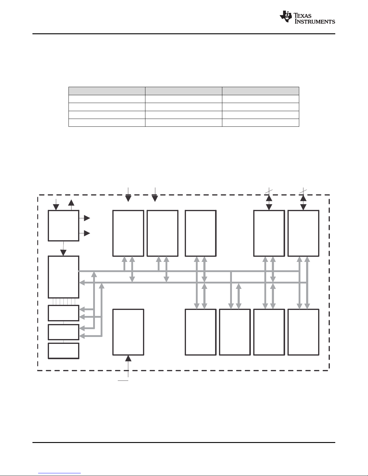
The MSP430G2x44 series is an ultra-low-power mixed-signal microcontroller with two built-in 16-bit timers,
a universal serial communication interface (USCI), 10-bit analog-to-digital converter (ADC) with integrated
reference and data transfer controller (DTC), and 32 I/O pins.
1
An IMPORTANT NOTICE at the end of this data sheet addresses availability, warranty, changes, use in safety-critical applications,
intellectual property matters and other important disclaimers. PRODUCTION DATA.
Basic Clock
System+
RAM
1KB
512B
512B
Brownout
Protection
RST/NMI
VCC VSS
MCLK
SMCLK
Watchdog
WDT+
15/16 Bit
Timer_A3
3 CC
Registers
16-MHz
CPU
incl.
16 Registers
Emulation
(2BP)
XOUT
JTAG
Interface
Flash
32KB
16KB
8KB
ACLK
XIN
MDB
MAB
Spy−Bi Wire
Timer_B3
3 CC
Registers,
Shadow
Reg
USCI_A0:
UART/LIN,
IrDA, SPI
USCI_B0:
SPI, I2C
ADC10
10 Bit
12 Channels
Autoscan
DTC
Ports P1/P2
2x8 I/O
Interrupt
capability,
pullup/down
resistors
P1.x/P2.x
2x8
P3.x/P4.x
2x8
Ports P3/P4
2x8 I/O
pullup/down
resistors
MSP430G2744, MSP430G2544, MSP430G2444
SLAS892C –MARCH 2013–REVISED SEPTEMBER 2014
Typical applications include sensor systems that capture analog signals, convert them to digital values,
and then process the data for display or for transmission to a host system. Stand-alone radio-frequency
(RF) sensor front ends are another area of application.
www.ti.com
PART NUMBER PACKAGE BODY SIZE
MSP430G2744DA TSSOP (38) 12.5 mm x 6.2 mm
MSP430G2744RHA VQFN (40) 6 mm xm 6 mm
MSP430G2744YFF DSBGA (49) 3.1 mm x 3.1 mm
PMS430G2744N PDIP (40) 52.46 mm x 13.71 mm
(1) For the most current part, package, and ordering information for all available devices, see the Package
Option Addendum in Section 8, or see the TI web site at www.ti.com.
(2) The sizes shown here are approximations. For the package dimensions with tolerances, see the
Mechanical Data in Section 8.
1.4 Functional Block Diagram
Figure 1-1 shows the functional block diagram of the MSP430G2x44 devices.
Device Information
(1)
(2)
Figure 1-1. Functional Block Diagram
2 Device Overview Copyright © 2013–2014, Texas Instruments Incorporated
Submit Documentation Feedback
Product Folder Links: MSP430G2744 MSP430G2544 MSP430G2444
MSP430G2744, MSP430G2544, MSP430G2444
www.ti.com
SLAS892C –MARCH 2013–REVISED SEPTEMBER 2014
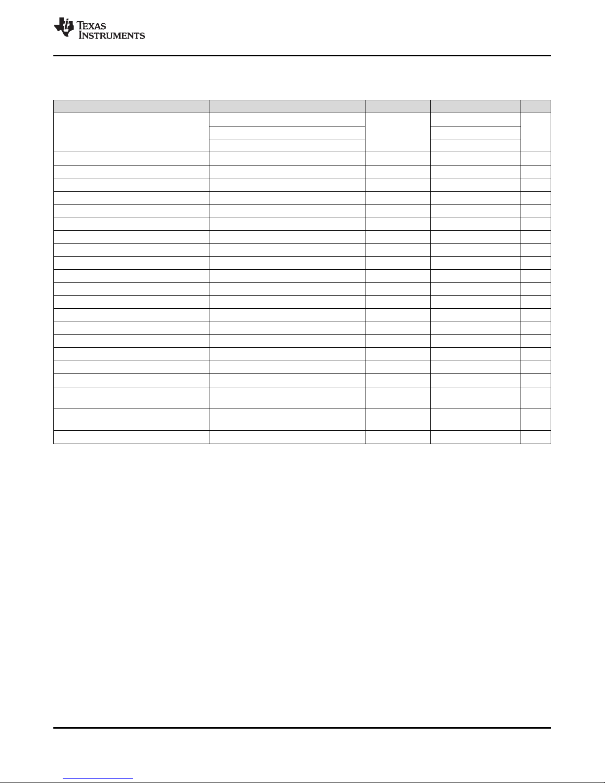
Table of Contents
1 Device Overview ......................................... 1 5.27 USCI (SPI Slave Mode)............................. 30
1.1 Features .............................................. 1 5.28 USCI (I2C Mode) .................................... 31
1.2 Applications........................................... 1
1.3 Description............................................ 1
1.4 Functional Block Diagram ............................ 2
2 Revision History ......................................... 4
3 Device Comparison ..................................... 5
4 Terminal Configuration and Functions.............. 6
4.1 Pin Diagrams ......................................... 6
4.2 Signal Descriptions.................................. 10
5 Specifications........................................... 13
5.1 Absolute Maximum Ratings......................... 13
5.2 Handling Ratings .................................... 13
5.3 Recommended Operating Conditions............... 13
5.4 Active Mode Supply Current (Into DVCC+ AVCC)
Excluding External Current.......................... 15
5.5 Typical Characteristics - Active-Mode Supply
Current (Into DVCC+ AV
5.6 Low-Power-Mode Supply Currents (Into VCC)
Excluding External Current.......................... 16
5.7 Schmitt-Trigger Inputs (Ports P1, P2, P3, P4, and
RST/NMI)............................................ 17
5.8 Leakage Current, Ports Px.......................... 17
5.9 Outputs, Ports Px ................................... 17
5.10 Output Frequency, Ports Px ........................ 17
5.11 Typical Characteristics - Outputs ................... 18
5.12 POR and BOR ...................................... 19
5.13 Typical Characteristics - POR and BOR ............ 20
5.14 DCO Frequency..................................... 21
5.15 Calibrated DCO Frequencies, Tolerance ........... 22
5.16 Wake-Up From Lower-Power Modes (LPM3,
LPM4) ............................................... 23
5.17 Typical Characteristics - DCO Clock Wake-Up Time
From LPM3 or LPM4................................ 23
5.18 DCO With External Resistor R
5.19 Typical Characteristics - DCO With External
Resistor R
5.20 Crystal Oscillator LFXT1, Low-Frequency Mode ... 25
5.21 Internal Very-Low-Power Low-Frequency Oscillator
(VLO)................................................ 25
5.22 Crystal Oscillator LFXT1, High-Frequency Mode... 26
5.23 Typical Characteristics - LFXT1 Oscillator in HF
Mode (XTS = 1) ..................................... 27
5.24 Timer_A, Timer_B................................... 28
5.25 USCI (UART Mode)................................. 28
5.26 USCI (SPI Master Mode)............................ 29
....................................... 24
OSC
)......................... 15 6.3 Operating Modes.................................... 40
CC
.................. 24
OSC
5.29 10-Bit ADC, Power Supply and Input Range
Conditions ........................................... 32
5.30 10-Bit ADC, Built-In Voltage Reference............. 33
5.31 10-Bit ADC, External Reference .................... 34
5.32 10-Bit ADC, Timing Parameters .................... 34
5.33 10-Bit ADC, Linearity Parameters................... 35
5.34 10-Bit ADC, Temperature Sensor and Built-In V
MID
...................................................... 35
5.35 Flash Memory ....................................... 36
5.36 RAM................................................. 36
5.37 JTAG and Spy-Bi-Wire Interface.................... 37
5.38 JTAG Fuse .......................................... 37
6 Detailed Description ................................... 38
6.1 CPU ................................................. 38
6.2 Instruction Set....................................... 39
6.4 Interrupt Vector Addresses.......................... 41
6.5 Special Function Registers.......................... 42
6.6 Memory Organization ............................... 43
6.7 Bootstrap Loader (BSL)............................. 43
6.8 Flash Memory ....................................... 43
6.9 Peripherals .......................................... 44
6.10 Oscillator and System Clock ........................ 44
6.11 Brownout ............................................ 44
6.12 Digital I/O............................................ 44
6.13 Watchdog Timer (WDT+) ........................... 44
6.14 Timer_A3............................................ 45
6.15 Timer_B3............................................ 46
6.16 Universal Serial Communications Interface (USCI). 46
6.17 ADC10............................................... 46
6.18 Peripheral File Map ................................. 47
6.19 Port Schematics..................................... 50
7 Device and Documentation Support ............... 69
7.1 Device Support...................................... 69
7.2 Documentation Support ............................. 72
7.3 Related Links........................................ 72
7.4 Community Resources .............................. 72
7.5 Trademarks.......................................... 72
7.6 Electrostatic Discharge Caution..................... 72
7.7 Glossary............................................. 72
8 Mechanical, Packaging, and Orderable
Information .............................................. 73
Copyright © 2013–2014, Texas Instruments Incorporated Table of Contents 3
Product Folder Links: MSP430G2744 MSP430G2544 MSP430G2444
Submit Documentation Feedback
MSP430G2744, MSP430G2544, MSP430G2444
SLAS892C –MARCH 2013–REVISED SEPTEMBER 2014
www.ti.com
2 Revision History
NOTE: Page numbers for previous revisions may differ from page numbers in the current version.
Changes from Revision B (March 2013) to Revision C Page
• Document formatting changes throughout, including addition of section numbering ........................................ 1
• Added Device Information table .................................................................................................... 2
• Added Section 3; moved and renamed Table 3-1................................................................................ 5
• Corrected size of RAM for MSP430G2744 in Table 3-1......................................................................... 5
• Added Section 5 and moved all electrical specifications to it ................................................................. 13
• Added Section 5.2 and moved T
• Added Section 7 and moved Tools Support, Device Nomenclature, ESD Caution, and Trademarks sections to it ... 69
• Added Section 8 .................................................................................................................... 73
to it .......................................................................................... 13
stg
4 Revision History Copyright © 2013–2014, Texas Instruments Incorporated
Product Folder Links: MSP430G2744 MSP430G2544 MSP430G2444
Submit Documentation Feedback
www.ti.com
3 Device Comparison
Table 3-1 summarizes the available family members.
MSP430G2744, MSP430G2544, MSP430G2444
SLAS892C –MARCH 2013–REVISED SEPTEMBER 2014
Table 3-1. Device Comparison
Device BSL EEM Timer_A Timer_B Clock I/O
MSP430G2744IRHA40 32 40-QFN
MSP430G2744IDA38 1 1 32 1K TA3 TB3 12 1 DCO, 32 38-TSSOP
MSP430G2744IYFF 32 49-DSBGA
MSP430G2544IRHA40 32 40-QFN
MSP430G2544IDA38 1 1 16 512 TA3 TB3 12 1 DCO, 32 38-TSSOP
MSP430G2544IYFF 32 49-DSBGA
MSP430G2444IRHA40 32 40-QFN
MSP430G2444IDA38 1 1 8 512 TA3 TB3 12 1 DCO, 32 38-TSSOP
MSP430G2444IYFF 32 49-DSBGA
Flash RAM ADC10 USCI_A0, Package
(KB) (B) Channel USCI_B0 Type
(1)(2)
HF, LF,
VLO
HF, LF,
VLO
HF, LF,
VLO
(1) For the most current package and ordering information, see the Package Option Addendum in Section 8, or see the TI web site at
www.ti.com.
(2) Package drawings, thermal data, and symbolization are available at www.ti.com/packaging.
Copyright © 2013–2014, Texas Instruments Incorporated Device Comparison 5
Product Folder Links: MSP430G2744 MSP430G2544 MSP430G2444
Submit Documentation Feedback
1TEST/SBWTCK
2DVCC
3P2.5/R
OSC
4
XOUT/P2.7
5
XIN/P2.6 6
RST/NMI/SBWTDIO
7
P2.0/ACLK/A0
8
P2.1/TAINCLK/SMCLK/A1 9
P2.2/TA0/A2
10
P3.0/UCB0STE/UCA0CLK/A5
11
P3.1/UCB0SIMO/UCB0SDA 12
P3.2/UCB0SOMI/UCB0SCL
13
P3.3/UCB0CLK/UCA0STE
14
P4.0/TB0
15
P4.1/TB1
16
P4.2/TB2
17
P4.3/TB0/A12
18 P4.4/TB1/A13
19
38 P1.7/TA2/TDO/TDI
37 P1.6/TA1/TDI
36
P1.5/TA0/TMS
35 P1.4/SMCLK/TCK
34
P1.3/TA2
33
P1.2/TA1
32 P1.1/TA0
31
P1.0/TACLK/ADC10CLK
30
P2.4/TA2/A4/VREF+/VeREF+
29 P2.3/TA1/A3/VREF−/VeREF−
28 P3.7/A7
27 P3.6/A6
26 P3.5/UCA0RXD/UCA0SOMI
25
P3.4/UCA0TXD/UCA0SIMO
24
23AVCC
22
AVSS
21
P4.7/TBCLK
20
P4.6/TBOUTH/A15
DVSS
P4.5/TB2/A14
MSP430G2744, MSP430G2544, MSP430G2444
SLAS892C –MARCH 2013–REVISED SEPTEMBER 2014
4 Terminal Configuration and Functions
4.1 Pin Diagrams
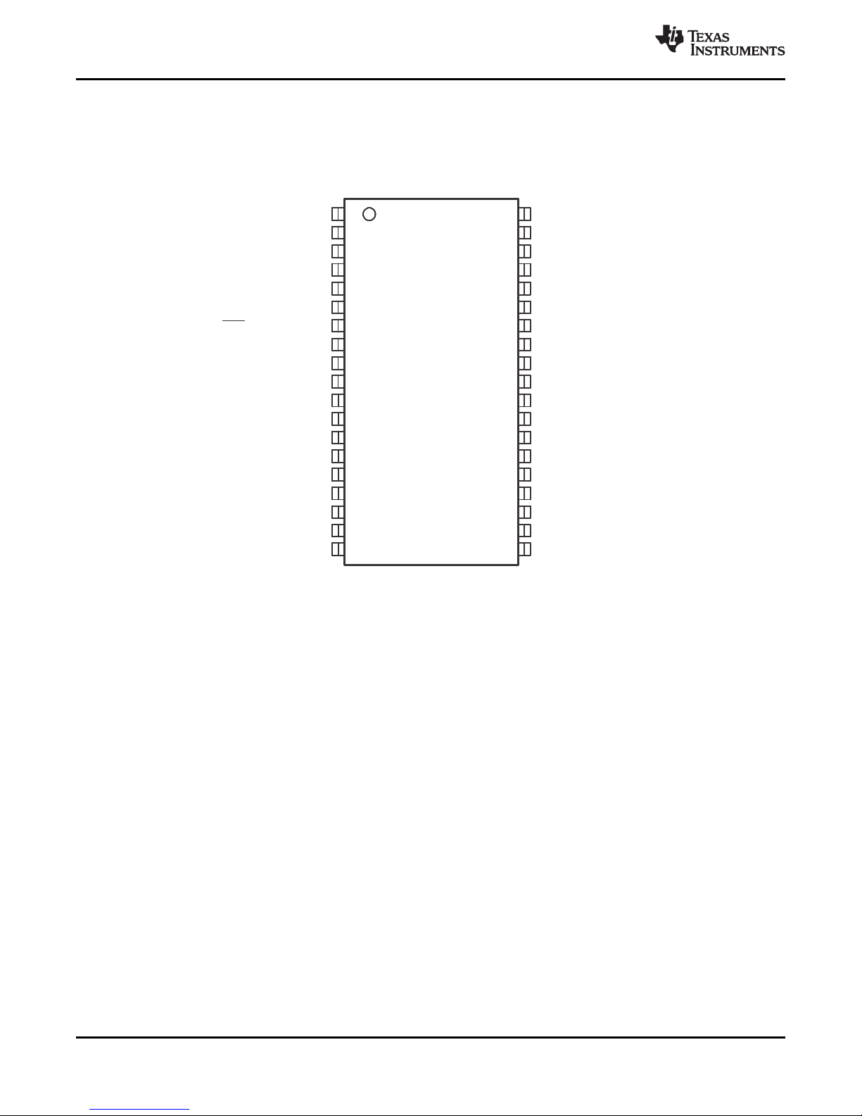
Figure 4-1 shows the pin diagram for the 38-pin DA package.
www.ti.com
Figure 4-1. 38-Pin TSSOP (DA Package) (Top View)
6 Terminal Configuration and Functions Copyright © 2013–2014, Texas Instruments Incorporated
Product Folder Links: MSP430G2744 MSP430G2544 MSP430G2444
Submit Documentation Feedback
1TEST/SBWTCK
2DVCC
3
P2.5/R
OSC
4
XOUT/P2.7
5
XIN/P2.6
6
RST/NMI/SBWTDIO
7
P2.0/ACLK/A0
8
P2.1/TAINCLK/SMCLK/A1
9
P2.2/TA0/A2
10
P3.0/UCB0STE/UCA0CLK/A5
11
P3.1/UCB0SIMO/UCB0SDA
12
P3.2/UCB0SOMI/UCB0SCL
13
P3.3/UCB0CLK/UCA0STE
14
P4.0/TB0
15
P4.1/TB1
16
P4.2/TB2
17
P4.3/TB0/A12
18
P4.4/TB1/A13
19
39
P1.7/TA2/TDO/TDI
38
P1.6/TA1/TDI
37
P1.5/TA0/TMS
36
P1.4/SMCLK/TCK
35
P1.3/TA2
34
P1.2/TA1
33
P1.1/TA0
32
P1.0/TACLK/ADC10CLK
31
P2.4/TA2/A4/VREF+/VeREF+
30
P2.3/TA1/A3/VREF−/VeREF−
29
P3.7/A7
28
P3.6/A6
27
P3.5/UCA0RXD/UCA0SOMI
26
P3.4/UCA0TXD/UCA0SIMO
25
24
AVCC
23
AVSS
22
P4.7/TBCLK
21
P4.6/TBOUTH/A15
DVSS
P4.5/TB2/A14
DVSS
20
DVCC
40
www.ti.com
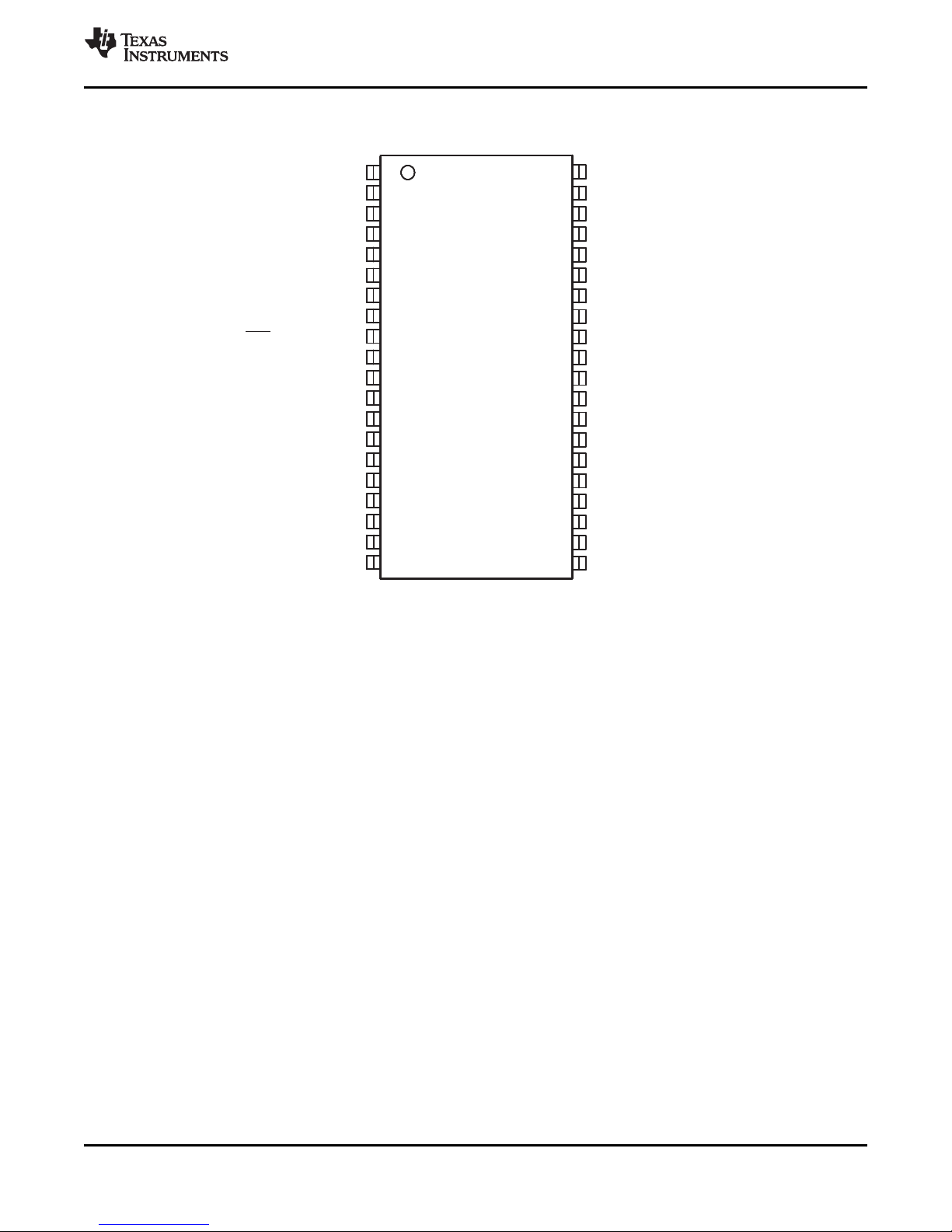
Figure 4-2 shows the pin diagram for the 40-pin N package.
MSP430G2744, MSP430G2544, MSP430G2444
SLAS892C –MARCH 2013–REVISED SEPTEMBER 2014
Figure 4-2. 40-Pin PDIP (N Package) (Top View)
Copyright © 2013–2014, Texas Instruments Incorporated Terminal Configuration and Functions 7
Product Folder Links: MSP430G2744 MSP430G2544 MSP430G2444
Submit Documentation Feedback
1DVSS
P1.5/TA0/TMS
P1.0/TACLK/ADC10CLK
P1.1/TA0
P1.2/TA1
P1.3/TA2
P1.4/SMCLK/TCK
13
P2.4/TA2/A4/VREF+/VeREF+
P2.5/R
OSC
DVCC
TEST/SBWTCK
P1.6/TA1/TDI/TCLK
2
3
4
5
6
7
8
10
9
12 14 15 16 17 18 19
30
29
28
27
26
25
24
23
21
22
3839 37 36 35 34 33 32
XOUT/P2.7
XIN/P2.6
DVSS
RST/NMI/SBWTDIO
P2.0/ACLK/A0
P2.1/TAINCLK/SMCLK/A1
P2.2/TA0/A2
P3.0/UCB0STE/UCA0CLK/A5
P3.1/UCB0SIMO/UCB0SDA
DVCC
P1.7/TA2/TDO/TDI
P2.3/TA1/A3/VREF−/VeREF−
P3.7/A7
P3.6/A6
P3.5/UCA0RXD/UCA0SOMI
P3.4/UCA0TXD/UCA0SIMO
AVCC
AVSS
P3.3/UCB0CLK/UCA0STE
P4.0/TB0
P4.1/TB1
P4.2/TB2
P4.3/TB0/A12
P4.4/TB1/A13
P4.5/TB2/A14
P4.6/TBOUTH/A15
P4.7/TBCLK
MSP430G2744, MSP430G2544, MSP430G2444
SLAS892C –MARCH 2013–REVISED SEPTEMBER 2014
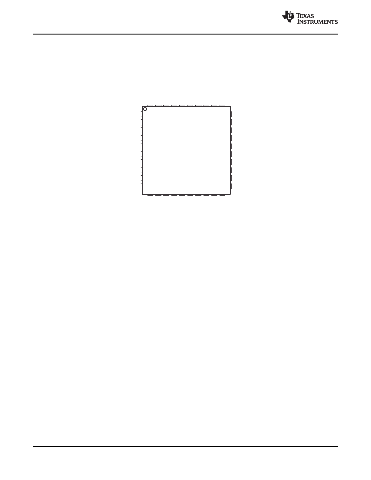
Figure 4-3 shows the pin diagram for the 40-pin RHA package.
www.ti.com
8 Terminal Configuration and Functions Copyright © 2013–2014, Texas Instruments Incorporated
Figure 4-3. 40-Pin QFN (RHA Package) (Top View)
Product Folder Links: MSP430G2744 MSP430G2544 MSP430G2444
Submit Documentation Feedback
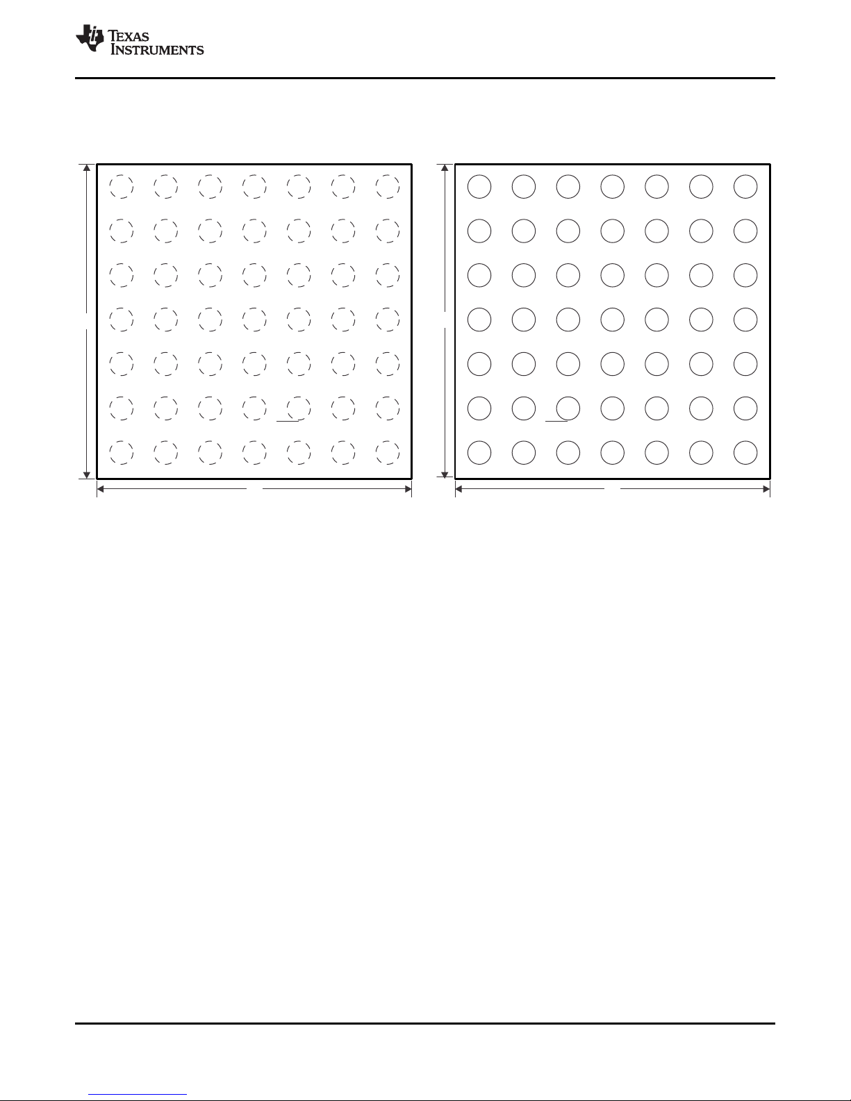
YFF PACKAGE
(TOP VIEW)
P2.0P2.2 P2.6 P2.7P3.1P3.2
DV
SS
A1A2
A4
A3
A5
A6
A7
B1B2
B4
B3
B5
B6
B7
C1C2C4
C3
C5C6C7
D1D2
D4
D3
D5
D6
D7
E1E2
E4
E3
E5
E6
E7
F1F2
F4
F3
F5
F6
F7
G1G2G4
G3
G5G6G7
P1.0
P1.1
P1.2
P1.3
P1.4
P1.5P1.6
P1.7
P2.1
P2.3
P2.4
P2.5
P3.0P3.3
P3.4 P3.5
P3.6
P3.7
P4.0P4.1
P4.2P4.3
P4.4 P4.5
P4.6
P4.7
RST/NMI
TEST
DV
CC
DV
CC
DV
CC
DV
CC
DV
CC
AV
CC
AV
CC
AV
CC
DV
SS
DV
SS
DV
SS
DV
SS
AV
SS
AV
SS
YFF PACKAGE
(BALL-SIDE VIEW)
P2.0 P2.2P2.6P2.7 P3.1 P3.2
DV
SS
A1 A2
A4
A3
A5
A6
A7
B1 B2
B4
B3
B5
B6
B7
C1 C2 C4
C3
C5 C6 C7
D1 D2
D4
D3
D5
D6
D7
E1 E2
E4
E3
E5
E6
E7
F1 F2
F4
F3
F5
F6
F7
G1 G2 G4
G3
G5 G6 G7
P1.0
P1.1
P1.2
P1.3
P1.4
P1.5 P1.6
P1.7
P2.1
P2.3
P2.4
P2.5
P3.0 P3.3
P3.4P3.5
P3.6
P3.7
P4.0 P4.1
P4.2 P4.3
P4.4P4.5
P4.6
P4.7
RST/NMI
TEST
DV
CC
DV
CC
DV
CC
DV
CC
DV
CC
AV
CC
AV
CC
AV
CC
DV
SS
DV
SS
DV
SS
DV
SS
AV
SS
AV
SS
D
E E
D
www.ti.com
Figure 4-4 shows the pin diagram for the 49-pin YFF package.
MSP430G2744, MSP430G2544, MSP430G2444
SLAS892C –MARCH 2013–REVISED SEPTEMBER 2014
Figure 4-4. 49-Pin DSBGA (YFF Package)
Copyright © 2013–2014, Texas Instruments Incorporated Terminal Configuration and Functions 9
Product Folder Links: MSP430G2744 MSP430G2544 MSP430G2444
Submit Documentation Feedback
MSP430G2744, MSP430G2544, MSP430G2444
SLAS892C –MARCH 2013–REVISED SEPTEMBER 2014
www.ti.com
4.2 Signal Descriptions
Table 4-1 describes the signals for all device variants and package options.
Table 4-1. Terminal Functions
TERMINAL
NAME
YFF DA N RHA
P1.0/TACLK/ADC10CLK F2 31 33 29 I/O Timer_A, clock signal TACLK input
P1.1/TA0 G2 32 34 30 I/O
P1.2/TA1 E2 33 35 31 I/O
P1.3/TA2 G1 34 36 32 I/O
P1.4/SMCLK/TCK F1 35 37 33 I/O SMCLK signal output
P1.5/TA0/TMS E1 36 38 34 I/O Timer_A, compare: OUT0 output
P1.6/TA1/TDI/TCLK E3 37 39 35 I/O Timer_A, compare: OUT1 output
P1.7/TA2/TDO/TDI
(1)
D2 38 40 36 I/O Timer_A, compare: OUT2 output
P2.0/ACLK/A0 A4 8 10 6 I/O ACLK output
P2.1/TAINCLK/
SMCLK/A1
B4 9 11 7 I/O Timer_A, clock signal at INCLK, SMCLK signal output
P2.2/TA0/A2 A5 10 12 8 I/O Timer_A, capture: CCI0B input; BSL receive, compare: OUT0 output
P2.3/TA1/A3/ V
P2.4/TA2/A4/
V
REF+/VeREF+
P2.5/R
OSC
REF-/VeREF-
F3 29 31 27 I/O
G3 30 32 28 I/O
C2 3 4 40 I/O
NO. I/O DESCRIPTION
General-purpose digital I/O pin
ADC10, conversion clock
General-purpose digital I/O pin
Timer_A, capture: CCI0A input, compare: OUT0 output; BSL transmit
General-purpose digital I/O pin
Timer_A, capture: CCI1A input, compare: OUT1 output
General-purpose digital I/O pin
Timer_A, capture: CCI2A input, compare: OUT2 output
General-purpose digital I/O pin
Test Clock input for device programming and test
General-purpose digital I/O pin
Test Mode Select input for device programming and test
General-purpose digital I/O pin
Test Data Input or Test Clock Input for programming and test
General-purpose digital I/O pin
Test Data Output or Test Data Input for programming and test
General-purpose digital I/O pin
ADC10, analog input A0
General-purpose digital I/O pin
ADC10, analog input A1
General-purpose digital I/O pin
ADC10, analog input A2
General-purpose digital I/O pin
Timer_A, capture CCI1B input, compare: OUT1 output
ADC10, analog input A3
Negative reference voltage output/input
General-purpose digital I/O pin
Timer_A, compare: OUT2 output
ADC10, analog input A4
Positive reference voltage output/input
General-purpose digital I/O pin
Input for external DCO resistor to define DCO frequency
(1) TDO or TDI is selected via JTAG instruction.
10 Terminal Configuration and Functions Copyright © 2013–2014, Texas Instruments Incorporated
Product Folder Links: MSP430G2744 MSP430G2544 MSP430G2444
Submit Documentation Feedback
MSP430G2744, MSP430G2544, MSP430G2444
www.ti.com
SLAS892C –MARCH 2013–REVISED SEPTEMBER 2014
Table 4-1. Terminal Functions (continued)
TERMINAL
NAME
YFF DA N RHA
XIN/P2.6 A2 6 7 3 I/O
XOUT/P2.7 A1 5 6 2 I/O
P3.0/UCB0STE/
UCA0CLK/A5
P3.1/UCB0SIMO/
UCB0SDA
P3.2/UCB0SOMI/
UCB0SCL
P3.3/UCB0CLK/
UCA0STE
P3.4/UCA0TXD/
UCA0SIMO
P3.5/UCA0RXD/
UCA0SOMI
B5 11 13 9 I/O
A6 12 14 10 I/O USCI_B0 slave in, master out in SPI mode
A7 13 15 11 I/O USCI_B0 slave out, master in SPI mode
B6 14 16 12 I/O USCI_B0 clock input/output
G6 25 27 23 I/O USCI_A0 transmit data output in UART mode
G5 26 28 24 I/O USCI_A0 receive data input in UART mode
P3.6/A6 F4 27 29 25 I/O
P3.7/A7 G4 28 30 26 I/O
P4.0/TB0 D6 17 19 15 I/O
P4.1/TB1 D7 18 20 16 I/O
P4.2/TB2 E6 19 21 17 I/O
P4.3/TB0/A12 E7 20 22 18 I/O Timer_B, capture: CCI0B input, compare: OUT0 output
P4.4/TB1/A13 F7 21 23 19 I/O Timer_B, capture: CCI1B input, compare: OUT1 output
P4.5/TB2/A14 F6 22 24 20 I/O Timer_B, compare: OUT2 output
NO. I/O DESCRIPTION
Input terminal of crystal oscillator
General-purpose digital I/O pin
Output terminal of crystal oscillator
General-purpose digital I/O pin
(2)
General-purpose digital I/O pin
USCI_B0 slave transmit enable
USCI_A0 clock input/output
ADC10, analog input A5
General-purpose digital I/O pin
USCI_B0 SDA I2C data in I2C mode
General-purpose digital I/O pin
USCI_B0 SCL I2C clock in I2C mode
General-purpose digital I/O pin
USCI_A0 slave transmit enable
General-purpose digital I/O pin
USCI_A0 slave in, master out in SPI mode
General-purpose digital I/O pin
USCI_A0 slave out, master in SPI mode
General-purpose digital I/O pin
ADC10 analog input A6
General-purpose digital I/O pin
ADC10 analog input A7
General-purpose digital I/O pin
Timer_B, capture: CCI0A input, compare: OUT0 output
General-purpose digital I/O pin
Timer_B, capture: CCI1A input, compare: OUT1 output
General-purpose digital I/O pin
Timer_B, capture: CCI2A input, compare: OUT2 output
General-purpose digital I/O pin
ADC10 analog input A12
General-purpose digital I/O pin
ADC10 analog input A13
General-purpose digital I/O pin
ADC10 analog input A14
(2) If XOUT/P2.7 is used as an input, excess current flows until P2SEL.7 is cleared. This is due to the oscillator output driver connection to
this pad after reset.
Copyright © 2013–2014, Texas Instruments Incorporated Terminal Configuration and Functions 11
Product Folder Links: MSP430G2744 MSP430G2544 MSP430G2444
Submit Documentation Feedback
MSP430G2744, MSP430G2544, MSP430G2444
SLAS892C –MARCH 2013–REVISED SEPTEMBER 2014
Table 4-1. Terminal Functions (continued)
TERMINAL
NAME
YFF DA N RHA
P4.6/TBOUTH/A15 G7 23 25 21 I/O Timer_B, switch all TB0 to TB3 outputs to high impedance
P4.7/TBCLK F5 24 26 22 I/O
RST/NMI/SBWTDIO B3 7 9 5 I
TEST/SBWTCK D1 1 1 37 I
C1,
D3,
DV
CC
D4, 2 2, 3 38, 39 Digital supply voltage
E4,
E5
C6,
AV
CC
C7, 16 18 14 Analog supply voltage
D5
A3,
B1,
DV
SS
B2, 4 5, 8 1, 4 Digital ground reference
C3,
C4
AV
SS
B7,
C5
QFN Pad NA NA NA Pad NA QFN package pad; connection to DVSSrecommended.
NO. I/O DESCRIPTION
General-purpose digital I/O pin
ADC10 analog input A15
General-purpose digital I/O pin
Timer_B, clock signal TBCLK input
Reset or nonmaskable interrupt input
Spy-Bi-Wire test data input/output during programming and test
Selects test mode for JTAG pins on Port 1. The device protection
fuse is connected to TEST.
Spy-Bi-Wire test clock input during programming and test
15 17 13 Analog ground reference
www.ti.com
12 Terminal Configuration and Functions Copyright © 2013–2014, Texas Instruments Incorporated
Product Folder Links: MSP430G2744 MSP430G2544 MSP430G2444
Submit Documentation Feedback
www.ti.com
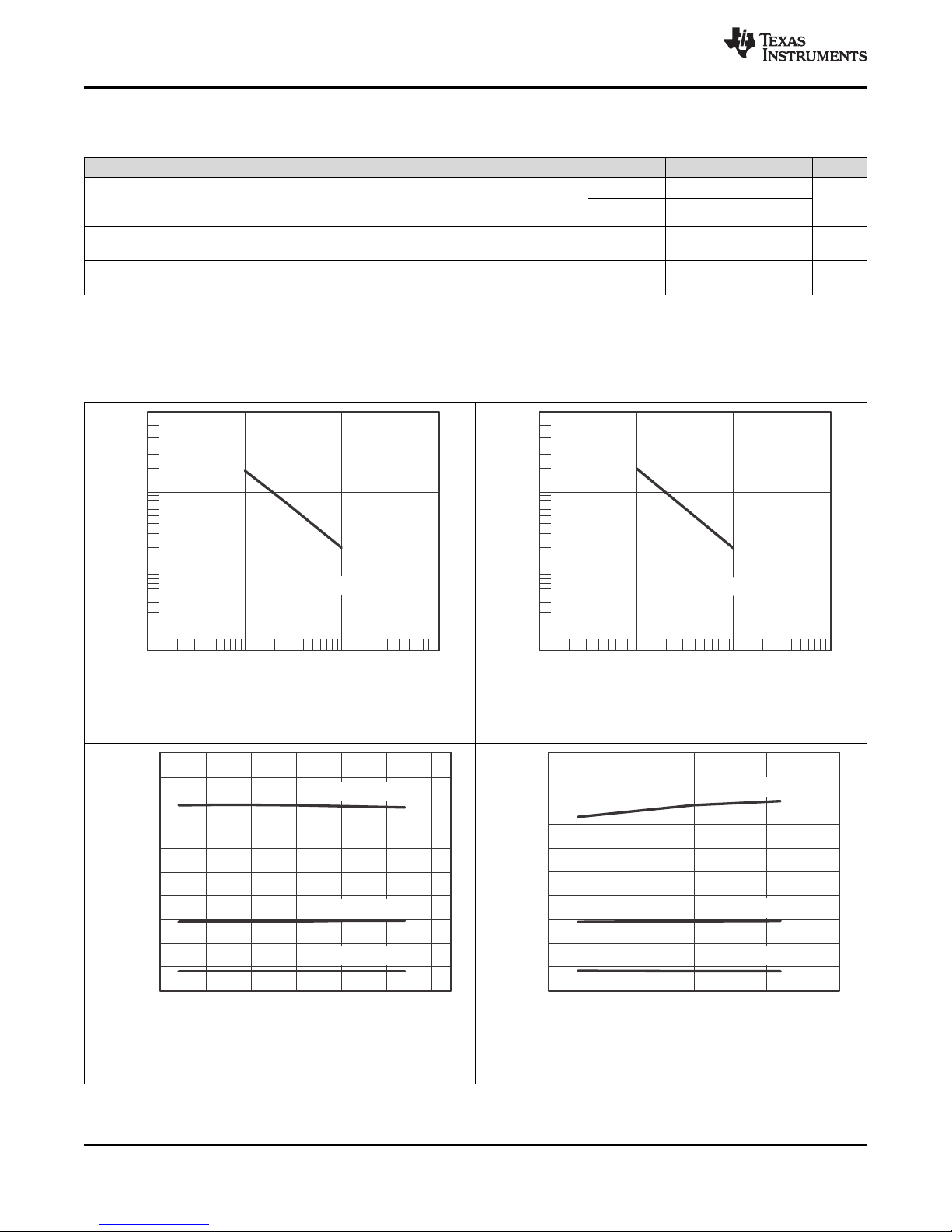
5 Specifications
MSP430G2744, MSP430G2544, MSP430G2444
SLAS892C –MARCH 2013–REVISED SEPTEMBER 2014
5.1 Absolute Maximum Ratings
(1)(2)
MIN MAX UNIT
Voltage applied at V
CC
Voltage applied to any pin
(3)
-0.3 4.1 V
-0.3 VCC+ 0.3 V
Diode current at any device terminal ±2 mA
(1) Stresses beyond those listed under Absolute Maximum Ratings may cause permanent damage to the device. These are stress ratings
only, and functional operation of the device at these or any other conditions beyond those indicated under Recommended Operating
Conditions is not implied. Exposure to absolute-maximum-rated conditions for extended periods may affect device reliability.
(2) All voltages referenced to VSS.
(3) The JTAG fuse-blow voltage, VFB, is allowed to exceed the absolute maximum rating. The voltage is applied to the TEST pin when
blowing the JTAG fuse.
5.2 Handling Ratings
MIN MAX UNIT
T
stg
Storage temperature (programmed or unprogrammed device)
(1) Higher temperature may be applied during board soldering process according to the current JEDEC J-STD-020 specification with peak
reflow temperatures not higher than classified on the device label on the shipping boxes or reels.
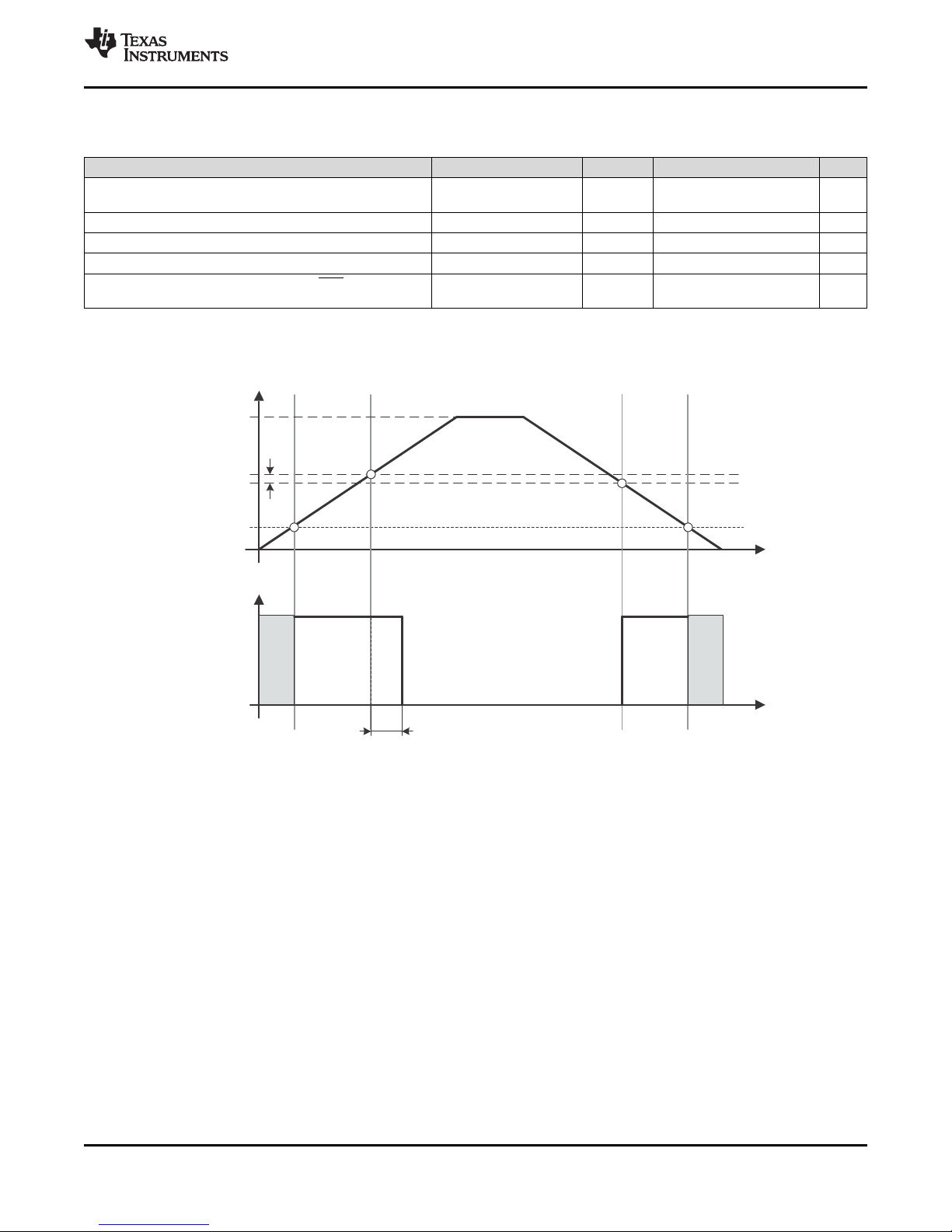
5.3 Recommended Operating Conditions
(1)(2)
Typical values are specified at VCC= 3.3 V and TA= 25°C (unless otherwise noted)
V
CC
V
SS
T
A
f
SYSTEM
(1) The MSP430 CPU is clocked directly with MCLK. Both the high and low phase of MCLK must not exceed the pulse width of the
specified maximum frequency.
(2) Modules might have a different maximum input clock specification. See the specification of the respective module in this data sheet.
Supply voltage AVCC= DVCC= V
Supply voltage AVSS= DVSS= V
CC
SS
Operating free-air temperature -40 85 °C
Processor frequency
(maximum MCLK frequency)
(see Figure 5-1)
VCC= 1.8 V, Duty cycle = 50% ±10% dc 4.15
(1)(2)
VCC= 2.7 V, Duty cycle = 50% ±10% dc 12 MHz
VCC≥ 3.3 V, Duty cycle = 50% ±10% dc 16
(1)
-55 150 °C
MIN NOM MAX UNIT
During program execution 1.8 3.6 V
During program and erase of
flash memory
2.2 3.6 V
0 V
Copyright © 2013–2014, Texas Instruments Incorporated Specifications 13
Product Folder Links: MSP430G2744 MSP430G2544 MSP430G2444
Submit Documentation Feedback
4.15 MHz
12 MHz
16 MHz
1.8 V 2.2 V 2.7 V 3.3 V 3.6 V
Supply Voltage − V
System Frequency – MHz
Supply voltage range
during flash memory
programming
Supply voltage range
during program execution
Legend:
7.5 MHz
MSP430G2744, MSP430G2544, MSP430G2444
SLAS892C –MARCH 2013–REVISED SEPTEMBER 2014
www.ti.com
NOTE: Minimum processor frequency is defined by system clock. Flash program or erase operations require a minimum V
of 2.2 V.
Figure 5-1. Operating Area
CC
14 Specifications Copyright © 2013–2014, Texas Instruments Incorporated
Product Folder Links: MSP430G2744 MSP430G2544 MSP430G2444
Submit Documentation Feedback
0.0
1.0
2.0
3.0
4.0
5.0
6.0
7.0
8.0
1.5 2.0 2.5 3.0 3.5 4.0
VCC− Supply Voltage − V
Active Mode Current − mA
f
DCO
= 1 MHz
f
DCO
= 8 MHz
f
DCO
= 12 MHz
f
DCO
= 16 MHz
0.0
1.0
2.0
3.0
4.0
5.0
0.0 4.0 8.0 12.0 16.0
f
DCO
− DCO Frequency − MHz
Active Mode Current − mA
TA= 25 °C
TA= 85 °C
VCC= 2.2 V
VCC= 3 V
TA= 25 °C
TA= 85 °C
www.ti.com
MSP430G2744, MSP430G2544, MSP430G2444
SLAS892C –MARCH 2013–REVISED SEPTEMBER 2014
5.4 Active Mode Supply Current (Into DVCC+ AVCC) Excluding External Current
(1)(2)
over recommended ranges of supply voltage and operating free-air temperature (unless otherwise noted)
I
AM,1MHz
PARAMETER TEST CONDITIONS T
f
= f
Active mode (AM)
current (1 MHz)
DCO
f
ACLK
Program executes in flash,
= f
MCLK
= 32768 Hz,
BCSCTL1 = CALBC1_1MHZ, µA
DCOCTL = CALDCO_1MHZ,
= 1 MHz, 2.2 V 270
SMCLK
A
CPUOFF = 0, SCG0 = 0, SCG1 = 0,
OSCOFF = 0
(1) All inputs are tied to 0 V or VCC. Outputs do not source or sink any current.
(2) The currents are characterized with a Micro Crystal CC4V-T1A SMD crystal with a load capacitance of 9 pF. The internal and external
load capacitance is chosen to closely match the required 9 pF.
V
CC
MIN TYP MAX UNIT
3 V 390 550
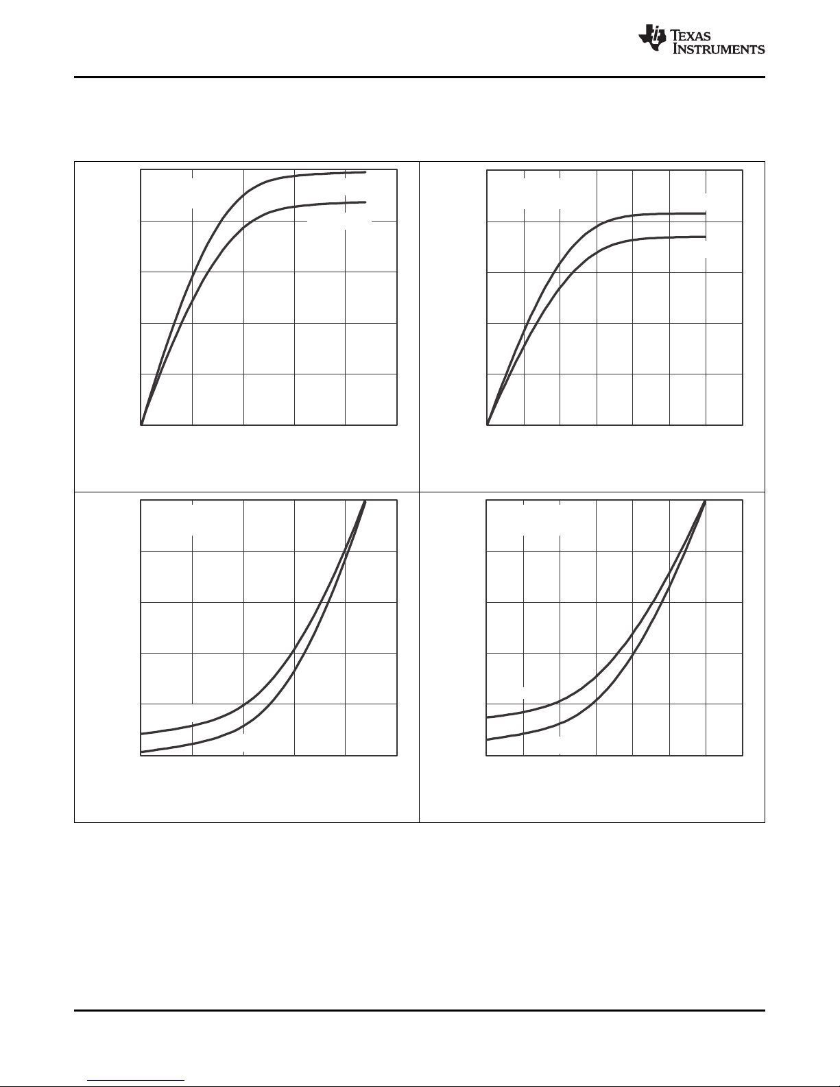
5.5 Typical Characteristics - Active-Mode Supply Current (Into DVCC+ AVCC)
TA= 25°C
Figure 5-2. Active-mode Current vs Supply Voltage Figure 5-3. Active-Mode Current vs DCO Frequency
Copyright © 2013–2014, Texas Instruments Incorporated Specifications 15
Product Folder Links: MSP430G2744 MSP430G2544 MSP430G2444
Submit Documentation Feedback
MSP430G2744, MSP430G2544, MSP430G2444
SLAS892C –MARCH 2013–REVISED SEPTEMBER 2014
www.ti.com
5.6 Low-Power-Mode Supply Currents (Into VCC) Excluding External Current
(1)(2)
over recommended ranges of supply voltage and operating free-air temperature (unless otherwise noted)
I
LPM0,1MHz
PARAMETER TEST CONDITIONS T
f
= 0 MHz,
MCLK
f
= f
= 1 MHz,
DCO
= 32768 Hz,
Low-power mode 0
(LPM0) current
(3)
SMCLK
f
ACLK
BCSCTL1 = CALBC1_1MHZ, 25°C 2.2 V 75 90 µA
DCOCTL = CALDCO_1MHZ,
A
CPUOFF = 1, SCG0 = 0,
SCG1 = 0, OSCOFF = 0
f
I
LPM2
Low-power mode 2
(LPM2) current
(4)
= f
MCLK
f
= 1 MHz,
DCO
f
= 32768 Hz,
ACLK
BCSCTL1 = CALBC1_1MHZ, 25°C 2.2 V 22 µA
DCOCTL = CALDCO_1MHZ,
SMCLK
= 0 MHz,
CPUOFF = 1, SCG0 = 0,
SCG1 = 1, OSCOFF = 0
f
= f
I
LPM3,LFXT1
Low-power mode 3 f
(LPM3) current
(4)
DCO
ACLK
CPUOFF = 1, SCG0 = 1,
= f
MCLK
= 32768 Hz,
SMCLK
= 0 MHz,
25°C 2.2 V 1 2 µA
SCG1 = 1, OSCOFF = 0
f
= f
I
LPM3,VLO
Low-power mode 3
current, (LPM3)
(4)
DCO
f
ACLK
(VLO), 25°C 2.2 V 0.5 1 µA
= f
MCLK
from internal LF oscillator
CPUOFF = 1, SCG0 = 1,
SMCLK
= 0 MHz,
SCG1 = 1, OSCOFF = 0
f
= f
I
LPM4
Low-power mode 4 f
(LPM4) current
(5)
MCLK
= 0 Hz,
= f
DCO
ACLK
CPUOFF = 1, SCG0 = 1,
SCG1 = 1, OSCOFF = 1
= 0 MHz, 25°C 0.1 0.5
SMCLK
85°C 1.5 3
(1) All inputs are tied to 0 V or VCC. Outputs do not source or sink any current.
(2) The currents are characterized with a Micro Crystal CC4V-T1A SMD crystal with a load capacitance of 9 pF. The internal and external
load capacitance is chosen to closely match the required 9 pF.
(3) Current for brownout and WDT clocked by SMCLK included.
(4) Current for brownout and WDT clocked by ACLK included.
(5) Current for brownout included.
V
MIN TYP MAX UNIT
CC
2.2 V µA
16 Specifications Copyright © 2013–2014, Texas Instruments Incorporated
Product Folder Links: MSP430G2744 MSP430G2544 MSP430G2444
Submit Documentation Feedback
MSP430G2744, MSP430G2544, MSP430G2444
www.ti.com
SLAS892C –MARCH 2013–REVISED SEPTEMBER 2014
5.7 Schmitt-Trigger Inputs (Ports P1, P2, P3, P4, and RST/NMI)
over recommended ranges of supply voltage and operating free-air temperature (unless otherwise noted)
PARAMETER TEST CONDITIONS V
V
Positive-going input threshold voltage V
IT+
V
Negative-going input threshold voltage V
IT-
V
Input voltage hysteresis (V
hys
R
Pullup or pulldown resistor 3 V 20 35 50 kΩ
Pull
C
Input capacitance VIN= VSSor V
I
IT+
- V
) 3 V 0.3 1 V
IT-
For pullup: VIN= VSS,
For pulldown: VIN= V
CC
CC
CC
3 V 1.35 2.25
3 V 0.75 1.65
MIN TYP MAX UNIT
0.45 V
0.25 V
CC
CC
0.75 V
0.55 V
5 pF
CC
CC
5.8 Leakage Current, Ports Px
over recommended ranges of supply voltage and operating free-air temperature (unless otherwise noted)
I
lkg(Px.y)
PARAMETER TEST CONDITIONS V
High-impedance leakage current
(1) (2)
CC
3 V ±50 nA
(1) The leakage current is measured with VSSor VCCapplied to the corresponding pin(s), unless otherwise noted.
(2) The leakage of the digital port pins is measured individually. The port pin is selected for input and the pullup or pulldown resistor is
disabled.
MIN TYP MAX UNIT
5.9 Outputs, Ports Px
over recommended ranges of supply voltage and operating free-air temperature (unless otherwise noted)
PARAMETER TEST CONDITIONS V
V
V
High-level output voltage I
OH
Low-level output voltage I
OL
(1) The maximum total current, I
specified.
OH(max)
and I
= -6 mA
OH(max)
= 6 mA
OL(max)
, for all outputs combined, should not exceed ±48 mA to hold the maximum voltage drop
OL(max)
(1)
(1)
CC
3 V VCC- 0.3 V
3 V VSS+ 0.3 V
MIN TYP MAX UNIT
5.10 Output Frequency, Ports Px
over recommended ranges of supply voltage and operating free-air temperature (unless otherwise noted)
f
Px.y
f
Port_CLK
PARAMETER TEST CONDITIONS V
Port output frequency (with load) 3 V 12 MHz
Clock output frequency Px.y, CL= 20 pF
Px.y, CL= 20 pF,
RL= 1 kΩ against VCC/2
(2)
(1)(2)
CC
3 V 16 MHz
(1) Alternatively, a resistive divider with two 2-kΩ resistors between VCCand VSSis used as load. The output is connected to the center tap
of the divider.
(2) The output voltage reaches at least 10% and 90% VCCat the specified toggle frequency.
MIN TYP MAX UNIT
Copyright © 2013–2014, Texas Instruments Incorporated Specifications 17
Product Folder Links: MSP430G2744 MSP430G2544 MSP430G2444
Submit Documentation Feedback
VOH− High-Level Output Voltage − V
−25.0
−20.0
−15.0
−10.0
−5.0
0.0
0.0 0.5 1.0 1.5 2.0 2.5
VCC= 2.2 V
P4.5
TA= 25°C
TA= 85°C
OH
I − Typical High-Level Output Current − mA
VOH− High-Level Output Voltage − V
−50.0
−40.0
−30.0
−20.0
−10.0
0.0
0.0 0.5 1.0 1.5 2.0 2.5 3.0 3.5
VCC= 3 V
P4.5
TA= 25°C
TA= 85°C
OH
I − Typical High-Level Output Current − mA
VOL− Low-Level Output V oltage − V
0.0
5.0
10.0
15.0
20.0
25.0
0.0 0.5 1.0 1.5 2.0 2.5
VCC= 2.2 V
P4.5
TA= 25°C
TA= 85°C
OL
I − Typical Low-Level Output Current − mA
VOL− Low-Level Output V oltage − V
0.0
10.0
20.0
30.0
40.0
50.0
0.0 0.5 1.0 1.5 2.0 2.5 3.0 3.5
VCC= 3 V
P4.5
TA= 25°C
TA= 85°C
OL
I − Typical Low-Level Output Current − mA
MSP430G2744, MSP430G2544, MSP430G2444
SLAS892C –MARCH 2013–REVISED SEPTEMBER 2014
5.11 Typical Characteristics - Outputs
One output loaded at a time.
www.ti.com
Figure 5-4. Typical Low-Level Output Current vs Low-Level Figure 5-5. Typical Low-Level Output Current vs Low-Level
Figure 5-6. Typical High-Level Output Current vs High-Level Figure 5-7. Typical High-Level Output Current vs High-Level
Output Voltage Output Voltage
Output Voltage Output Voltage
18 Specifications Copyright © 2013–2014, Texas Instruments Incorporated
Product Folder Links: MSP430G2744 MSP430G2544 MSP430G2444
Submit Documentation Feedback
0
1
t
d(BOR)
V
CC
V
(B_IT−)
V
hys(B_IT−)
V
CC(star t)
www.ti.com
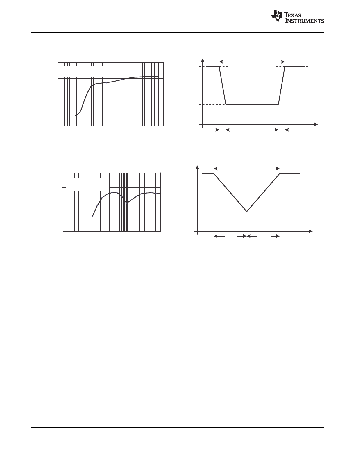
MSP430G2744, MSP430G2544, MSP430G2444
SLAS892C –MARCH 2013–REVISED SEPTEMBER 2014
5.12 POR and BOR
(1)(2)
over recommended ranges of supply voltage and operating free-air temperature (unless otherwise noted)
V
CC(start)
V
(B_IT-)
V
hys(B_IT-)
t
d(BOR)
t
(reset)
PARAMETER TEST CONDITIONS V
See Figure 5-8 dVCC/dt ≤ 3 V/s V
See Figure 5-8 through Figure 5-10 dVCC/dt ≤ 3 V/s 1.35 V
See Figure 5-8 dVCC/dt ≤ 3 V/s 140 mV
See Figure 5-8 2000 µs
Pulse duration needed at RST/NMI pin to
accept reset internally
CC
2.2 V 2 µs
(1) The current consumption of the brownout module is already included in the ICCcurrent consumption data. The voltage level V
V
hys(B_IT-)
(2) During power up, the CPU begins code execution following a period of t
must not be changed until VCC≥ V
is ≤ 1.8 V.
CC(min)
, where V
after VCC= V
is the minimum supply voltage for the desired operating frequency.
CC(min)
d(BOR)
(B_IT-)
MIN TYP MAX UNIT
0.7 ×
V
(B_IT-)
+ V
hys(B_IT-)
. The default DCO settings
(B_IT-)
+
Copyright © 2013–2014, Texas Instruments Incorporated Specifications 19
Product Folder Links: MSP430G2744 MSP430G2544 MSP430G2444
Figure 5-8. POR and BOR vs Supply Voltage
Submit Documentation Feedback
V
CC
0
0.5
1
1.5
2
V
CC(drop)
t
pw
tpw− Pulse Width − µs
V
CC(drop)
− V
3 V
0.001 1 1000
t
f
t
r
tpw− Pulse Width − µs
tf= t
r
Typical Conditions
VCC= 3 V
V
CC(drop)
V
CC
3 V
t
pw
0
0.5
1
1.5
2
0.001 1 1000
Typical Conditions
1 ns 1 ns
tpw− Pulse Width − µs
V
CC(drop)
− V
tpw− Pulse Width − µs
VCC= 3 V
MSP430G2744, MSP430G2544, MSP430G2444
SLAS892C –MARCH 2013–REVISED SEPTEMBER 2014
5.13 Typical Characteristics - POR and BOR
www.ti.com
Figure 5-9. V
Figure 5-10. V
CC(drop)
CC(drop)
Level With a Square Voltage Drop to Generate a POR or BOR Signal
Level With a Triangular Voltage Drop to Generate a POR or BOR Signal
20 Specifications Copyright © 2013–2014, Texas Instruments Incorporated
Product Folder Links: MSP430G2744 MSP430G2544 MSP430G2444
Submit Documentation Feedback
MSP430G2744, MSP430G2544, MSP430G2444
www.ti.com
SLAS892C –MARCH 2013–REVISED SEPTEMBER 2014
5.14 DCO Frequency
over recommended ranges of supply voltage and operating free-air temperature (unless otherwise noted)
V
CC
f
DCO(0,0)
f
DCO(0,3)
f
DCO(1,3)
f
DCO(2,3)
f
DCO(3,3)
f
DCO(4,3)
f
DCO(5,3)
f
DCO(6,3)
f
DCO(7,3)
f
DCO(8,3)
f
DCO(9,3)
f
DCO(10,3)
f
DCO(11,3)
f
DCO(12,3)
f
DCO(13,3)
f
DCO(14,3)
f
DCO(15,3)
f
DCO(15,7)
S
RSEL
S
DCO
PARAMETER TEST CONDITIONS V
CC
RSELx < 14 1.8 3.6
Supply voltage range RSELx = 14 2.2 3.6 V
RSELx = 15 3.0 3.6
DCO frequency (0, 0) RSELx = 0, DCOx = 0, MODx = 0 3 V 0.06 0.14 MHz
DCO frequency (0, 3) RSELx = 0, DCOx = 3, MODx = 0 3 V 0.07 0.17 MHz
DCO frequency (1, 3) RSELx = 1, DCOx = 3, MODx = 0 3 V MHz
DCO frequency (2, 3) RSELx = 2, DCOx = 3, MODx = 0 3 V MHz
DCO frequency (3, 3) RSELx = 3, DCOx = 3, MODx = 0 3 V MHz
DCO frequency (4, 3) RSELx = 4, DCOx = 3, MODx = 0 3 V MHz
DCO frequency (5, 3) RSELx = 5, DCOx = 3, MODx = 0 3 V MHz
DCO frequency (6, 3) RSELx = 6, DCOx = 3, MODx = 0 3 V 0.54 1.06 MHz
DCO frequency (7, 3) RSELx = 7, DCOx = 3, MODx = 0 3 V 0.80 1.50 MHz
DCO frequency (8, 3) RSELx = 8, DCOx = 3, MODx = 0 3 V 1.6 MHz
DCO frequency (9, 3) RSELx = 9, DCOx = 3, MODx = 0 3 V 2.3 MHz
DCO frequency (10, 3) RSELx = 10, DCOx = 3, MODx = 0 3 V 3.4 MHz
DCO frequency (11, 3) RSELx = 11, DCOx = 3, MODx = 0 3 V 4.25 MHz
DCO frequency (12, 3) RSELx = 12, DCOx = 3, MODx = 0 3 V 4.30 7.30 MHz
DCO frequency (13, 3) RSELx = 13, DCOx = 3, MODx = 0 3 V 6.00 9.60 MHz
DCO frequency (14, 3) RSELx = 14, DCOx = 3, MODx = 0 3 V 8.60 13.9 MHz
DCO frequency (15, 3) RSELx = 15, DCOx = 3, MODx = 0 3 V 12.0 18.5 MHz
DCO frequency (15, 7) RSELx = 15, DCOx = 7, MODx = 0 3 V 16.0 26.0 MHz
Frequency step between
range RSEL and RSEL+1
Frequency step between tap
DCO and DCO+1
S
S
= f
RSEL
DCO(RSEL+1,DCO)/fDCO(RSEL,DCO)
= f
DCO
DCO(RSEL,DCO+1)/fDCO(RSEL,DCO)
3 V 1.35 ratio
3 V 1.08 ratio
Duty cycle Measured at SMCLK 3 V 50%
MIN TYP MAX UNIT
Copyright © 2013–2014, Texas Instruments Incorporated Specifications 21
Product Folder Links: MSP430G2744 MSP430G2544 MSP430G2444
Submit Documentation Feedback
MSP430G2744, MSP430G2544, MSP430G2444
SLAS892C –MARCH 2013–REVISED SEPTEMBER 2014
5.15 Calibrated DCO Frequencies, Tolerance
over recommended ranges of supply voltage and operating free-air temperature (unless otherwise noted)
PARAMETER TEST CONDITIONS T
1-MHz tolerance over
temperature
(1)
BCSCTL1 = CALBC1_1MHZ,
DCOCTL = CALDCO_1MHZ, 0°C to 85°C 3 V -3% ±0.5% +3%
calibrated at 30°C and 3 V
A
BCSCTL1 = CALBC1_1MHZ,
1-MHz tolerance over V
CC
DCOCTL = CALDCO_1MHZ, 30°C 1.8 V to 3.6 V -3% ±2% +3%
calibrated at 30°C and 3 V
BCSCTL1 = CALBC1_1MHZ,
1-MHz tolerance overall DCOCTL = CALDCO_1MHZ, -40°C to 85°C 1.8 V to 3.6 V -6% ±3% +6%
calibrated at 30°C and 3 V
8-MHz tolerance over
temperature
(1)
BCSCTL1 = CALBC1_8MHZ,
DCOCTL = CALDCO_8MHZ, 0°C to 85°C 3 V -3% ±0.5% +3%
calibrated at 30°C and 3 V
BCSCTL1 = CALBC1_8MHZ,
8-MHz tolerance over V
CC
DCOCTL = CALDCO_8MHZ, 30°C 2.2 V to 3.6 V -3% ±2% +3%
calibrated at 30°C and 3 V
BCSCTL1 = CALBC1_8MHZ,
8-MHz tolerance overall DCOCTL = CALDCO_8MHZ, -40°C to 85°C 2.2 V to 3.6 V -6% ±3% +6%
calibrated at 30°C and 3 V
12-MHz tolerance over
temperature
(1)
BCSCTL1 = CALBC1_12MHZ,
DCOCTL = CALDCO_12MHZ, 0°C to 85°C 3 V -3% ±0.5% +3%
calibrated at 30°C and 3 V
BCSCTL1 = CALBC1_12MHZ,
12-MHz tolerance over V
CC
DCOCTL = CALDCO_12MHZ, 30°C 2.7 V to 3.6 V -3% ±2% +3%
calibrated at 30°C and 3 V
BCSCTL1 = CALBC1_12MHZ,
12-MHz tolerance overall DCOCTL = CALDCO_12MHZ, -40°C to 85°C 2.7 V to 3.6 V -6% ±3% +6%
calibrated at 30°C and 3 V
16-MHz tolerance over
temperature
(1)
BCSCTL1 = CALBC1_16MHZ,
DCOCTL = CALDCO_16MHZ, 0°C to 85°C 3 V -3% ±0.5% +3%
calibrated at 30°C and 3 V
BCSCTL1 = CALBC1_16MHZ,
16-MHz tolerance over V
CC
DCOCTL = CALDCO_16MHZ, 30°C 3.3 V to 3.6 V -3% ±2% +3%
calibrated at 30°C and 3 V
BCSCTL1 = CALBC1_16MHZ,
16-MHz tolerance overall DCOCTL = CALDCO_16MHZ, -40°C to 85°C 3.3 V to 3.6 V -6% ±3% +6%
calibrated at 30°C and 3 V
(1) This is the frequency change from the measured frequency at 30°C over temperature.
V
CC
MIN TYP MAX UNIT
www.ti.com
22 Specifications Copyright © 2013–2014, Texas Instruments Incorporated
Product Folder Links: MSP430G2744 MSP430G2544 MSP430G2444
Submit Documentation Feedback

DCO Frequency − MHz
0.10
1.00
10.00
0.10 1.00 10.00
RSELx = 0...11
RSELx = 12...15
DCO Wake-Up Time − µs
MSP430G2744, MSP430G2544, MSP430G2444
www.ti.com
SLAS892C –MARCH 2013–REVISED SEPTEMBER 2014
5.16 Wake-Up From Lower-Power Modes (LPM3, LPM4)
over recommended ranges of supply voltage and operating free-air temperature (unless otherwise noted)
t
DCO,LPM3/4
t
CPU,LPM3/4
PARAMETER TEST CONDITIONS V
DCO clock wake-up time BCSCTL1 = CALBC1_1MHZ,
from LPM3 or LPM4
CPU wake-up time from 1 / f
LPM3 or LPM4
(1)
(2)
DCOCTL = CALDCO_1MHZ
CC
3 V 1.5 µs
(1) The DCO clock wake-up time is measured from the edge of an external wake-up signal (for example, a port interrupt) to the first clock
edge observable externally on a clock pin (MCLK or SMCLK).
(2) Parameter applicable only if DCOCLK is used for MCLK.
MIN TYP MAX UNIT
+
MCLK
t
Clock,LPM3/4
5.17 Typical Characteristics - DCO Clock Wake-Up Time From LPM3 or LPM4
Figure 5-11. Clock Wake-Up Time From LPM3 vs DCO Frequency
Copyright © 2013–2014, Texas Instruments Incorporated Specifications 23
Product Folder Links: MSP430G2744 MSP430G2544 MSP430G2444
Submit Documentation Feedback
0.00
0.25
0.50
0.75
1.00
1.25
1.50
1.75
2.00
2.25
2.50
−50.0 −25.0 0.0 25.0 50.0 75.0 100.0
T
− Temperature − °C
DCO Frequency − MHz
R
OSC
= 100k
R
OSC
= 270k
R
OSC
= 1M
0.00
0.25
0.50
0.75
1.00
1.25
1.50
1.75
2.00
2.25
2.50
2.0 2.5 3.0 3.5 4.0
VCC− Supply Voltage − V
DCO Frequency − MHz
R
OSC
= 100k
R
OSC
= 270k
R
OSC
= 1M
0.01
0.10
1.00
10.00
10.00 100.00 1000.00 10000.00
R
OSC
− External Resistor − kW
DCO Frequency − MHz
RSELx = 4
0.01
0.10
1.00
10.00
10.00 100.00 1000.00 10000.00
R
OSC
− External Resistor − kW
DCO Frequency − MHz
RSELx = 4
MSP430G2744, MSP430G2544, MSP430G2444
SLAS892C –MARCH 2013–REVISED SEPTEMBER 2014
www.ti.com
5.18 DCO With External Resistor R
OSC
(1)
over recommended ranges of supply voltage and operating free-air temperature (unless otherwise noted)
PARAMETER TEST CONDITIONS V
DCOR = 1, 2.2 V 1.8
f
DCO,ROSC
D
T
D
V
(1) R
DCO output frequency with R
OSC
Temperature drift 2.2 V, 3 V ±0.1 %/°C
Drift with V
= 100 kΩ. Metal film resistor, type 0257, 0.6 W with 1% tolerance and TK= ±50 ppm/°C.
OSC
CC
RSELx = 4, DCOx = 3, MODx = 0, MHz
TA= 25°C
DCOR = 1,
RSELx = 4, DCOx = 3, MODx = 0
DCOR = 1,
RSELx = 4, DCOx = 3, MODx = 0
5.19 Typical Characteristics - DCO With External Resistor R
CC
3 V 1.95
2.2 V, 3 V 10 %/V
OSC
MIN TYP MAX UNIT
VCC= 2.2 V TA= 25°C VCC= 3 V TA= 25°C
Figure 5-12. DCO Frequency vs R
VCC= 3 V TA= 25°C
Figure 5-14. DCO Frequency vs Temperature Figure 5-15. DCO Frequency vs Supply Voltage
24 Specifications Copyright © 2013–2014, Texas Instruments Incorporated
Product Folder Links: MSP430G2744 MSP430G2544 MSP430G2444
OSC
Submit Documentation Feedback
Figure 5-13. DCO Frequency vs R
OSC

www.ti.com
MSP430G2744, MSP430G2544, MSP430G2444
SLAS892C –MARCH 2013–REVISED SEPTEMBER 2014
5.20 Crystal Oscillator LFXT1, Low-Frequency Mode
(1)
over recommended ranges of supply voltage and operating free-air temperature (unless otherwise noted)
f
LFXT1,LF
PARAMETER TEST CONDITIONS V
LFXT1 oscillator crystal
frequency, LF mode 0, 1
XTS = 0, LFXT1Sx = 0 or 1 1.8 V to 3.6 V 32768 Hz
CC
LFXT1 oscillator logic level
f
LFXT1,LF,logic
square wave input frequency, XTS = 0, XCAPx = 0, LFXT1Sx = 3 1.8 V to 3.6 V 10000 32768 50000 Hz
LF mode
XTS = 0, LFXT1Sx = 0,
OA
LF
Oscillation allowance for
LF crystals
f
XTS = 0, LFXT1Sx = 0,
f
LFXT1,LF
LFXT1,LF
= 32768 Hz, C
= 32768 Hz, C
L,eff
L,eff
= 6 pF
= 12 pF
XTS = 0, XCAPx = 0 1
C
L,eff
Integrated effective load
capacitance, LF mode
(2)
XTS = 0, XCAPx = 1 5.5
XTS = 0, XCAPx = 2 8.5
XTS = 0, XCAPx = 3 11
XTS = 0, Measured at P2.0/ACLK,
f
LFXT1,LF
= 32768 Hz
XTS = 0, XCAPx = 0, LFXT1Sx = 3
(4)
2.2 V 10 10000 Hz
f
Fault,LF
Duty cycle, LF mode 2.2 V 30% 50% 70%
Oscillator fault frequency,
LF mode
(3)
(1) To improve EMI on the XT1 oscillator, the following guidelines should be observed.
• Keep the trace between the device and the crystal as short as possible.
• Design a good ground plane around the oscillator pins.
• Prevent crosstalk from other clock or data lines into oscillator pins XIN and XOUT.
• Avoid running PCB traces underneath or adjacent to the XIN and XOUT pins.
• Use assembly materials and processes that avoid any parasitic load on the oscillator XIN and XOUT pins.
• If conformal coating is used, make sure that it does not induce capacitive or resistive leakage between the oscillator pins.
• Do not route the XOUT line to the JTAG header to support the serial programming adapter as shown in other documentation. This
signal is no longer required for the serial programming adapter.
(2) Includes parasitic bond and package capacitance (approximately 2 pF per pin).
Because the PCB adds additional capacitance, it is recommended to verify the correct load by measuring the ACLK frequency. For a
correct setup, the effective load capacitance should always match the specification of the crystal that is used.
(3) Frequencies below the MIN specification set the fault flag. Frequencies above the MAX specification do not set the fault flag.
Frequencies between the MIN and MAX specifications might set the flag.
(4) Measured with logic-level input frequency but also applies to operation with crystals.
MIN TYP MAX UNIT
500
200
kΩ
pF
5.21 Internal Very-Low-Power Low-Frequency Oscillator (VLO)
over recommended ranges of supply voltage and operating free-air temperature (unless otherwise noted)
PARAMETER T
f
VLO
df
/dT VLO frequency temperature drift
VLO
df
/dV
VLO
CC
VLO frequency -40°C to 85°C 3 V 4 12 20 kHz
VLO frequency supply voltage drift
(1)
(2)
A
-40°C to 85°C 3 V 0.5 %/°C
25°C 1.8 V to 3.6 V 4 %/V
(1) Calculated using the box method:
I version: [MAX(-40...85°C) - MIN(-40...85°C)]/MIN(-40...85°C)/[85°C - (-40°C)]
(2) Calculated using the box method: [MAX(1.8...3.6 V) - MIN(1.8...3.6 V)]/MIN(1.8...3.6 V)/(3.6 V - 1.8 V)
Copyright © 2013–2014, Texas Instruments Incorporated Specifications 25
Submit Documentation Feedback
Product Folder Links: MSP430G2744 MSP430G2544 MSP430G2444
V
CC
MIN TYP MAX UNIT

MSP430G2744, MSP430G2544, MSP430G2444
SLAS892C –MARCH 2013–REVISED SEPTEMBER 2014
www.ti.com
5.22 Crystal Oscillator LFXT1, High-Frequency Mode
PARAMETER TEST CONDITIONS V
f
LFXT1,HF0
f
LFXT1,HF1
LFXT1 oscillator crystal frequency,
HF mode 0
LFXT1 oscillator crystal frequency,
HF mode 1
XTS = 1, LFXT1Sx = 0 1.8 V to 3.6 V 0.4 1 MHz
XTS = 1, LFXT1Sx = 1 1.8 V to 3.6 V 1 4 MHz
(1)
CC
MIN TYP MAX UNIT
1.8 V to 3.6 V 2 10
f
LFXT1,HF2
LFXT1 oscillator crystal frequency,
HF mode 2
XTS = 1, LFXT1Sx = 2 2.2 V to 3.6 V 2 12 MHz
3 V to 3.6 V 2 16
1.8 V to 3.6 V 0.4 10
f
LFXT1,HF,logic
LFXT1 oscillator logic-level squarewave input frequency, HF mode
XTS = 1, LFXT1Sx = 3 2.2 V to 3.6 V 0.4 12 MHz
3 V to 3.6 V 0.4 16
XTS = 1, LFXT1Sx = 0,
OA
f
LFXT1,HF
C
HF
Oscillation allowance for HF crystals
(see Figure 5-16 and Figure 5-17)
XTS = 1, LFXT1Sx = 1,
f
LFXT1,HF
C
= 1 MHz, 2700
= 15 pF
L,eff
= 4 MHz, 800 Ω
= 15 pF
L,eff
XTS = 1, LFXT1Sx = 2,
f
LFXT1,HF
C
C
L,eff
Integrated effective load capacitance,
HF mode
(2)
XTS = 1
= 16 MHz, 300
= 15 pF
L,eff
(3)
1 pF
XTS = 1,
Measured at P2.0/ACLK, 40% 50% 60%
f
Duty cycle, HF mode 2.2 V
LFXT1,HF
XTS = 1,
= 10 MHz
Measured at P2.0/ACLK, 40% 50% 60%
f
Fault,HF
Oscillator fault frequency
f
(4)
LFXT1,HF
XTS = 1, LFXT1Sx = 3
= 16 MHz
(5)
2.2 V 30 300 kHz
(1) To improve EMI on the XT1 oscillator the following guidelines should be observed:
• Keep the trace between the device and the crystal as short as possible.
• Design a good ground plane around the oscillator pins.
• Prevent crosstalk from other clock or data lines into oscillator pins XIN and XOUT.
• Avoid running PCB traces underneath or adjacent to the XIN and XOUT pins.
• Use assembly materials and processes that avoid any parasitic load on the oscillator XIN and XOUT pins.
• If conformal coating is used, make sure that it does not induce capacitive or resistive leakage between the oscillator pins.
• Do not route the XOUT line to the JTAG header to support the serial programming adapter as shown in other documentation. This
signal is no longer required for the serial programming adapter.
(2) Includes parasitic bond and package capacitance (approximately 2 pF per pin). Because the PCB adds additional capacitance, it is
recommended to verify the correct load by measuring the ACLK frequency. For a correct setup, the effective load capacitance should
always match the specification of the used crystal.
(3) Requires external capacitors at both terminals. Values are specified by crystal manufacturers.
(4) Frequencies below the MIN specification set the fault flag. Frequencies above the MAX specification do not set the fault flag.
Frequencies between the MIN and MAX specifications might set the flag.
(5) Measured with logic-level input frequency, but also applies to operation with crystals.
26 Specifications Copyright © 2013–2014, Texas Instruments Incorporated
Product Folder Links: MSP430G2744 MSP430G2544 MSP430G2444
Submit Documentation Feedback

0.0
100.0
200.0
300.0
400.0
500.0
600.0
700.0
800.0
0.0 4.0 8.0 12.0 16.0 20.0
Crystal Frequency − MHz
XT Oscillator Supply Current − uA
LFXT1Sx = 1
LFXT1Sx = 3
LFXT1Sx = 2
Crystal Frequency − MHz
10.00
100.00
1000.00
10000.00
100000.00
0.10 1.00 10.00 100.00
Oscillation Allowance − Ohms
LFXT1Sx = 1
LFXT1Sx = 3
LFXT1Sx = 2
MSP430G2744, MSP430G2544, MSP430G2444
www.ti.com
SLAS892C –MARCH 2013–REVISED SEPTEMBER 2014
5.23 Typical Characteristics - LFXT1 Oscillator in HF Mode (XTS = 1)
C
= 15 pF TA= 25°C
L,eff
Figure 5-16. Oscillation Allowance vs Crystal Frequency
C
= 15 pF TA= 25°C
L,eff
Figure 5-17. Oscillator Supply Current vs Crystal Frequency
Copyright © 2013–2014, Texas Instruments Incorporated Specifications 27
Product Folder Links: MSP430G2744 MSP430G2544 MSP430G2444
Submit Documentation Feedback

MSP430G2744, MSP430G2544, MSP430G2444
SLAS892C –MARCH 2013–REVISED SEPTEMBER 2014
5.24 Timer_A, Timer_B
over recommended ranges of supply voltage and operating free-air temperature (unless otherwise noted)
f
TA
t
TA,cap
PARAMETER TEST CONDITIONS V
CC
Timer_A clock frequency SMCLK, Duty cycle = 50% ± 10% f
Timer_A capture timing TAx, TBx 3 V 20 ns
MIN TYP MAX UNIT
SYSTEM
5.25 USCI (UART Mode)
over recommended ranges of supply voltage and operating free-air temperature (unless otherwise noted)
PARAMETER TEST CONDITIONS V
Internal: SMCLK, ACLK
f
USCI
f
max,BITCLK
t
τ
USCI input clock frequency External: UCLK f
Duty cycle = 50% ± 10%
Maximum BITCLK clock frequency
(equals baud rate in MBaud)
UART receive deglitch time
(1)
(1) The DCO wake-up time must be considered in LPM3/4 for baud rates above 1 MHz.
CC
3 V 2 MHz
3 V 50 100 600 ns
MIN TYP MAX UNIT
SYSTEM
www.ti.com
MHz
MHz
28 Specifications Copyright © 2013–2014, Texas Instruments Incorporated
Product Folder Links: MSP430G2744 MSP430G2544 MSP430G2444
Submit Documentation Feedback

UCLK
CKPL=0
CKPL=1
SIMO
1/f
UCxCLK
t
LO/HItLO/HI
SOMI
t
SU,MI
t
HD,MI
t
VALID,MO
UCLK
CKPL=0
CKPL=1
SIMO
1/f
UCxCLK
t
LO/HItLO/HI
SOMI
t
SU,MI
t
HD,MI
t
VALID,MO
www.ti.com
MSP430G2744, MSP430G2544, MSP430G2444
SLAS892C –MARCH 2013–REVISED SEPTEMBER 2014
5.26 USCI (SPI Master Mode)
(1)
over recommended ranges of supply voltage and operating free-air temperature (unless otherwise noted)
(see Figure 5-18 and Figure 5-19)
PARAMETER TEST CONDITIONS V
f
USCI
t
SU,MI
t
HD,MI
t
VALID,MO
(1) f
For the slave parameters t
USCI input clock frequency SMCLK, duty cycle = 50% ± 10% f
SOMI input data setup time 3 V 75 ns
SOMI input data hold time 3 V 0 ns
SIMO output data valid time UCLK edge to SIMO valid,CL= 20 pF 3 V 20 ns
= 1/2t
UCxCLK
LO/HI
with t
≥ max(t
LO/HI
SU,SI(Slave)
VALID,MO(USCI)
and t
VALID,SO(Slave)
+ t
SU,SI(Slave)
, t
, see the SPI parameters of the attached slave.
SU,MI(USCI)
+ t
VALID,SO(Slave)
).
CC
MIN TYP MAX UNIT
SYSTEM
MHz
Figure 5-18. SPI Master Mode, CKPH = 0
Figure 5-19. SPI Master Mode, CKPH = 1
Copyright © 2013–2014, Texas Instruments Incorporated Specifications 29
Product Folder Links: MSP430G2744 MSP430G2544 MSP430G2444
Submit Documentation Feedback

STE
UCLK
CKPL=0
CKPL=1
t
STE,LEAD
t
STE,LAG
t
STE,ACC
t
STE,DIS
t
LO/HItLO/HI
t
SU,SI
t
HD,SI
t
VALID,SO
SOMI
SIMO
1/f
UCxCLK
STE
UCLK
CKPL=0
CKPL=1
SOMI
t
STE,ACC
t
STE,DIS
1/f
UCxCLK
t
LO/HItLO/HI
SIMO
t
SU,SI
t
HD,SI
t
VALID,SO
t
STE,LEAD
t
STE,LAG
MSP430G2744, MSP430G2544, MSP430G2444
SLAS892C –MARCH 2013–REVISED SEPTEMBER 2014
www.ti.com
5.27 USCI (SPI Slave Mode)
(1)
over recommended ranges of supply voltage and operating free-air temperature (unless otherwise noted)
(see Figure 5-20 and Figure 5-21)
t
STE,LEAD
t
STE,LAG
t
STE,ACC
t
STE,DIS
t
SU,SI
t
HD,SI
t
VALID,SO
(1) f
STE lead time, STE low to clock 3 V 50 ns
STE lag time, Last clock to STE high 3 V 10 ns
STE access time, STE low to SOMI data out 3 V 50 ns
STE disable time, STE high to SOMI high
impedance
SIMO input data setup time 3 V 15 ns
SIMO input data hold time 3 V 10 ns
SOMI output data valid time 3 V 50 75 ns
= 1/2t
UCxCLK
For the master's parameters t
LO/HI
PARAMETER TEST CONDITIONS V
UCLK edge to SOMI valid,
CL= 20 pF
with t
LO/HI
≥ max(t
VALID,MO(Master)
SU,MI(Master)
and t
VALID,MO(Master)
+ t
SU,SI(USCI)
, t
SU,MI(Master)
refer to the SPI parameters of the attached slave.
+ t
VALID,SO(USCI)
CC
3 V 50 ns
).
MIN TYP MAX UNIT
30 Specifications Copyright © 2013–2014, Texas Instruments Incorporated
Product Folder Links: MSP430G2744 MSP430G2544 MSP430G2444
Figure 5-20. SPI Slave Mode, CKPH = 0
Figure 5-21. SPI Slave Mode, CKPH = 1
Submit Documentation Feedback

SDA
SCL
1/f
SCL
t
HD,DAT
t
SU,DAT
t
HD,STA
t
SU,STAtHD,STA
t
SU,STO
t
SP
MSP430G2744, MSP430G2544, MSP430G2444
www.ti.com
SLAS892C –MARCH 2013–REVISED SEPTEMBER 2014
5.28 USCI (I2C Mode)
over recommended ranges of supply voltage and operating free-air temperature (unless otherwise noted) (see Figure 5-22)
f
USCI
f
SCL
t
HD,STA
t
SU,STA
t
HD,DAT
t
SU,DAT
t
SU,STO
t
SP
PARAMETER TEST CONDITIONS V
CC
Internal: SMCLK, ACLK
USCI input clock frequency External: UCLK f
Duty cycle = 50% ± 10%
SCL clock frequency 3 V 0 400 kHz
f
≤ 100 kHz 4
Hold time (repeated) START 3 V µs
Setup time for a repeated START 3 V µs
SCL
f
> 100 kHz 0.6
SCL
f
≤ 100 kHz 4.7
SCL
f
> 100 kHz 0.6
SCL
Data hold time 3 V 0 ns
Data setup time 3 V 250 ns
Setup time for STOP 3 V 4 µs
Pulse duration of spikes suppressed by
input filter
3 V 50 100 600 ns
MIN TYP MAX UNIT
SYSTEM
MHz
Figure 5-22. I2C Mode Timing
Copyright © 2013–2014, Texas Instruments Incorporated Specifications 31
Product Folder Links: MSP430G2744 MSP430G2544 MSP430G2444
Submit Documentation Feedback

MSP430G2744, MSP430G2544, MSP430G2444
SLAS892C –MARCH 2013–REVISED SEPTEMBER 2014
www.ti.com
5.29 10-Bit ADC, Power Supply and Input Range Conditions
over recommended ranges of supply voltage and operating free-air temperature (unless otherwise noted)
PARAMETER TEST CONDITIONS T
V
V
I
ADC10
Analog supply voltage range VSS= 0 V 2.2 3.6 V
CC
Analog input voltage
Ax
range
ADC10 supply current
(2)
(3)
All Ax terminals,
Analog inputs selected in 3 V 0 V
ADC10AE register
f
ADC10CLK
ADC10ON = 1, REFON = 0,
= 5 MHz,
ADC10SHT0 = 1, 25°C 3 V 0.6 mA
ADC10SHT1 = 0,
(1)
(1)
A
V
CC
MIN TYP MAX UNIT
CC
ADC10DIV = 0
I
REF+
Reference supply current,
reference buffer disabled
f
ADC10CLK
ADC10ON = 0, REF2_5V = 0, 0.25
REFON = 1, REFOUT = 0
(4)
f
ADC10CLK
ADC10ON = 0, REF2_5V = 1, 0.25
= 5 MHz,
= 5 MHz,
25°C 3 V mA
REFON = 1, REFOUT = 0
I
REFB,0
I
REFB,1
C
I
R
I
f
Reference buffer supply
current with 25°C 3 V 1.1 mA
ADC10SR = 0
(4)
Reference buffer supply
current with 25°C 3 V 0.5 mA
ADC10SR = 1
(4)
Input capacitance 25°C 3 V 27 pF
ADC10CLK
ADC10ON = 0, REFON = 1,
REF2_5V = 0, REFOUT = 1,
ADC10SR = 0
f
ADC10CLK
ADC10ON = 0, REFON = 1,
REF2_5V = 0, REFOUT = 1,
ADC10SR = 1
Only one terminal Ax selected at
a time
Input MUX ON resistance 0 V ≤ VAx≤ V
= 5 MHz
= 5 MHz,
CC
25°C 3 V 1000 Ω
(1) The leakage current is defined in the leakage current table with Px.x/Ax parameter.
(2) The analog input voltage range must be within the selected reference voltage range VR+to VR-for valid conversion results.
(3) The internal reference supply current is not included in current consumption parameter I
(4) The internal reference current is supplied from terminal AVCC. Consumption is independent of the ADC10ON control bit, unless a
ADC10
.
conversion is active. The REFON bit enables the built-in reference to settle before starting an A/D conversion.
V
32 Specifications Copyright © 2013–2014, Texas Instruments Incorporated
Product Folder Links: MSP430G2744 MSP430G2544 MSP430G2444
Submit Documentation Feedback

MSP430G2744, MSP430G2544, MSP430G2444
www.ti.com
SLAS892C –MARCH 2013–REVISED SEPTEMBER 2014
5.30 10-Bit ADC, Built-In Voltage Reference
over recommended ranges of supply voltage and operating free-air temperature (unless otherwise noted)
PARAMETER TEST CONDITIONS V
I
≤ 1 mA, REF2_5V = 0 2.2
V
CC,REF+
V
REF+
I
LD,VREF+
Positive built-in reference
analog supply voltage range
Positive built-in reference
voltage
Maximum VREF+ load
current
VREF+ load regulation LSB
VREF+
I
≤ 1 mA, REF2_5V = 1 2.9
VREF+
I
≤ I
VREF+
I
VREF+
I
VREF+
Analog input voltage VAx≈ 0.75 V, 3 V ±2
max, REF2_5V = 0 3 V 1.41 1.5 1.59
VREF+
≤ I
max, REF2_5V = 1 3 V 2.35 2.5 2.65
VREF+
= 500 µA ± 100 µA,
REF2_5V = 0
I
= 500 µA ± 100 µA,
VREF+
Analog input voltage VAx≈ 1.25 V, 3 V ±2
REF2_5V = 1
I
= 100 µA to 900 µA,
VREF+ load regulation VAx≈ 0.5 x V
response time Error of conversion result ≤1 LSB,
VREF+
REF+
,
ADC10SR = 0
C
VREF+
TC
REF+
t
REFON
t
REFBURST
Maximum capacitance at pin I
VREF+ REFON = 1, REFOUT = 1
Temperature coefficient
(1)
Settling time of internal I
reference voltage REFON = 0 to 1
Settling time of reference REF2_5V = 1,
buffer to 99.9% VREF REFON = 1,
≤ ±1 mA,
VREF+
I
= constant with
VREF+
0 mA ≤ I
VREF+
I
VREF+
≤ 1 mA
VREF+
= 0.5 mA, REF2_5V = 0,
= 0.5 mA,
REFBURST = 1, ADC10SR = 0
(1) Calculated using the box method:
I temperature: (MAX(-40 to 85°C) – MIN(-40 to 85°C)) / MIN(-40 to 85°C) / (85°C – (–40°C))
CC
3 V ±1 mA
3 V 400 ns
3 V 100 pF
3 V ±100 ppm/°C
3.6 V 30 µs
3 V 2 µs
MIN TYP MAX UNIT
V
V
Copyright © 2013–2014, Texas Instruments Incorporated Specifications 33
Product Folder Links: MSP430G2744 MSP430G2544 MSP430G2444
Submit Documentation Feedback

MSP430G2744, MSP430G2544, MSP430G2444
SLAS892C –MARCH 2013–REVISED SEPTEMBER 2014
www.ti.com
5.31 10-Bit ADC, External Reference
(1)
over recommended ranges of supply voltage and operating free-air temperature (unless otherwise noted)
V
eREF+
V
eREF-
ΔV
eREF
I
VeREF+
I
VeREF-
PARAMETER TEST CONDITIONS V
V
> V
eREF+
Positive external reference input
voltage range
Negative external reference input
voltage range
(2)
(4)
SREF1 = 1, SREF0 = 0
V
≤ V
eREF-
SREF1 = 1, SREF0 = 1
V
eREF+
Differential external reference input
voltage range V
ΔVeREF = VeREF+ - VeREF-
eREF+
0 V ≤ V
Static input current into VeREF+ µA
SREF1 = 1, SREF0 = 0
0 V ≤ V
SREF1 = 1, SREF0 = 1
Static input current into VeREF- 0 V ≤ V
,
eREF-
≤ VCC- 0.15 V,
eREF+
> V
eREF-
> V
eREF-
(5)
eREF-
≤ VCC,
eREF+
≤ VCC- 0.15 V ≤ 3 V,
eREF+
≤ V
CC
(3)
(3)
CC
3 V ±1
3 V 0
3 V ±1 µA
(1) The external reference is used during conversion to charge and discharge the capacitance array. The input capacitance, CI, is also the
dynamic load for an external reference during conversion. The dynamic impedance of the reference supply should follow the
recommendations on analog-source impedance to allow the charge to settle for 10-bit accuracy.
(2) The accuracy limits the minimum positive external reference voltage. Lower reference voltage levels may be applied with reduced
accuracy requirements.
(3) Under this condition, the external reference is internally buffered. The reference buffer is active and requires the reference buffer supply
current I
(4) The accuracy limits the maximum negative external reference voltage. Higher reference voltage levels may be applied with reduced
. The current consumption can be limited to the sample and conversion period with REBURST = 1.
REFB
accuracy requirements.
(5) The accuracy limits the minimum external differential reference voltage. Lower differential reference voltage levels may be applied with
reduced accuracy requirements.
MIN TYP MAX UNIT
1.4 V
CC
V
1.4 3
0 1.2 V
1.4 V
CC
V
5.32 10-Bit ADC, Timing Parameters
over recommended ranges of supply voltage and operating free-air temperature (unless otherwise noted)
PARAMETER TEST CONDITIONS V
f
ADC10CLK
f
ADC10OSC
ADC10 input clock For specified performance of
frequency ADC10 linearity parameters
ADC10 built-in oscillator ADC10DIVx = 0, ADC10SSELx = 0,
frequency f
ADC10CLK
= f
ADC10OSC
ADC10 built-in oscillator, ADC10SSELx = 0,
t
CONVERT
t
ADC10ON
f
Conversion time µs
Turn on settling time of
the ADC
(1)
ADC10CLK
f
ADC10CLK
ADC10SSELx ≠ 0 1 / f
= f
ADC10OSC
from ACLK, MCLK or SMCLK, 13 × ADC10DIVx ×
(1) The condition is that the error in a conversion started after t
settled.
ADC10ON
CC
ADC10SR = 0 0.45 6.3
ADC10SR = 1 0.45 1.5
2.2 V, 3 V MHz
2.2 V, 3 V 3.7 6.3 MHz
2.2 V, 3 V 2.06 3.51
is less than ±0.5 LSB. The reference and input signal are already
MIN TYP MAX UNIT
ADC10CLK
100 ns
34 Specifications Copyright © 2013–2014, Texas Instruments Incorporated
Product Folder Links: MSP430G2744 MSP430G2544 MSP430G2444
Submit Documentation Feedback
www.ti.com
MSP430G2744, MSP430G2544, MSP430G2444
SLAS892C –MARCH 2013–REVISED SEPTEMBER 2014
5.33 10-Bit ADC, Linearity Parameters
(1)
over recommended ranges of supply voltage and operating free-air temperature (unless otherwise noted)
PARAMETER TEST CONDITIONS V
E
E
E
E
E
Integral linearity error SREFx = 010 3 V ±1 LSB
I
Differential linearity error SREFx = 010 3 V ±1 LSB
D
Offset error Source impedance RS< 100 Ω, SREFx = 010 3 V ±1 LSB
O
Gain error SREFx = 010 3 V ±1.1 ±2 LSB
G
Total unadjusted error SREFx = 010 3 V ±2 ±6 LSB
T
CC
(1) Using the integrated reference buffer (SREFx = 010) increases the gain, and offset and total unadjusted error.
5.34 10-Bit ADC, Temperature Sensor and Built-In V
MID
(1)
MIN TYP MAX UNIT
over recommended ranges of supply voltage and operating free-air temperature (unless otherwise noted)
PARAMETER TEST CONDITIONS V
I
SENSOR
TC
SENSOR
t
SENSOR(sample)
I
VMID
V
MID
t
VMID(sample)
(1) The sensor current I
high).When REFON = 1, I
input (INCH = 0Ah).
Temperature sensor supply REFON = 0, INCHx = 0Ah,
(1)
current
Sample time required if ADC10ON = 1, INCHx = 0Ah,
channel 10 is selected
(3)
Current into divider at
channel 11
VCCdivider at channel 11 3 V 1.5 V
Sample time required if ADC10ON = 1, INCHx = 0Bh,
channel 11 is selected
is consumed if (ADC10ON = 1 and REFON = 1), or (ADC10ON = 1 and INCH = 0Ah and sample signal is
SENSOR
SENSOR
(4)
is included in I
TA= 25°C
ADC10ON = 1, INCHx = 0Ah
(2)
Error of conversion result ≤ 1 LSB
ADC10ON = 1, INCHx = 0Bh 3 V
ADC10ON = 1, INCHx = 0Bh,
V
≈ 0.5 × V
MID
CC
Error of conversion result ≤ 1 LSB
.When REFON = 0, I
REF+
applies during conversion of the temperature sensor
SENSOR
(2) The following formula can be used to calculate the temperature sensor output voltage:
V
Sensor,typ
V
Sensor,typ
(3) No additional current is needed. The V
(4) The on time, t
= TC
= TC
( 273 + T [°C] ) + V
Sensor
T [°C] + V
Sensor
, is included in the sampling time, t
VMID(on)
Sensor(TA
MID
Offset,sensor
= 0°C) [mV]
[mV] or
is used during sampling.
VMID(sample)
; no additional on time is needed.
CC
3 V 60 µA
3 V 3.55 mV/°C
3 V 30 µs
3 V 1220 ns
MIN TYP MAX UNIT
(3)
µA
Copyright © 2013–2014, Texas Instruments Incorporated Specifications 35
Product Folder Links: MSP430G2744 MSP430G2544 MSP430G2444
Submit Documentation Feedback

MSP430G2744, MSP430G2544, MSP430G2444
SLAS892C –MARCH 2013–REVISED SEPTEMBER 2014
www.ti.com
5.35 Flash Memory
over recommended ranges of supply voltage and operating free-air temperature (unless otherwise noted)
PARAMETER TEST
CONDITIONS
V
CC (PGM/ERASE)
f
FTG
I
PGM
I
ERASE
t
CPT
t
CMErase
Program and erase supply voltage 2.2 3.6 V
Flash timing generator frequency 257 476 kHz
Supply current from VCCduring program 2.2 V, 3.6 V 1 5 mA
Supply current from VCCduring erase 2.2 V, 3.6 V 1 7 mA
Cumulative program time
(1)
Cumulative mass erase time 2.2 V, 3.6 V 20 ms
Program and erase endurance 10
t
Retention
t
Word
t
Block, 0
t
Block, 1-63
t
Block, End
t
Mass Erase
t
Seg Erase
Data retention duration TJ= 25°C 100 years
Word or byte program time
Block program time for first byte or word
Block program time for each additional byte or
word
Block program end-sequence wait time
Mass erase time
Segment erase time
(2)
(2)
(2)
(2)
(2)
(2)
(1) The cumulative program time must not be exceeded when writing to a 64-byte flash block. This parameter applies to all programming
methods: individual word write, individual byte write, and block write modes.
(2) These values are hardwired into the state machine of the flash controller (t
FTG
= 1/f
FTG
V
CC
MIN TYP MAX UNIT
2.2 V, 3.6 V 10 ms
4
10
5
cycles
30 t
25 t
18 t
6 t
10593 t
4819 t
).
FTG
FTG
FTG
FTG
FTG
FTG
5.36 RAM
over recommended ranges of supply voltage and operating free-air temperature (unless otherwise noted)
PARAMETER TEST CONDITIONS MIN MAX UNIT
V
(RAMh)
RAM retention supply voltage
(1) This parameter defines the minimum supply voltage VCCwhen the data in RAM remains unchanged. No program execution should
happen during this supply voltage condition.
(1)
CPU halted 1.6 V
36 Specifications Copyright © 2013–2014, Texas Instruments Incorporated
Product Folder Links: MSP430G2744 MSP430G2544 MSP430G2444
Submit Documentation Feedback

MSP430G2744, MSP430G2544, MSP430G2444
www.ti.com
SLAS892C –MARCH 2013–REVISED SEPTEMBER 2014
5.37 JTAG and Spy-Bi-Wire Interface
over recommended ranges of supply voltage and operating free-air temperature (unless otherwise noted)
PARAMETER V
f
SBW
t
SBW,Low
t
SBW,En
t
SBW,Ret
f
TCK
R
Internal
Spy-Bi-Wire input frequency 2.2 V 0 20 MHz
Spy-Bi-Wire low clock pulse duration 2.2 V 0.025 15 µs
Spy-Bi-Wire enable time
(TEST high to acceptance of first clock edge
(1)
)
Spy-Bi-Wire return to normal operation time 2.2 V 15 100 µs
TCK input frequency
(2)
Internal pulldown resistance on TEST 2.2 V 25 60 90 kΩ
(1) Tools accessing the Spy-Bi-Wire interface need to wait for the maximum t
applying the first SBWTCK clock edge.
(2) f
5.38 JTAG Fuse
may be restricted to meet the timing requirements of the module selected.
TCK
(1)
time after pulling the TEST/SBWTCK pin high before
SBW,En
CC
2.2 V 1 µs
2.2 V 0 5 MHz
over recommended ranges of supply voltage and operating free-air temperature (unless otherwise noted)
PARAMETER TEST CONDITIONS MIN MAX UNIT
V
CC(FB)
V
FB
I
FB
t
FB
Supply voltage during fuse-blow condition TA= 25°C 2.5 V
Voltage level on TEST for fuse blow 6 7 V
Supply current into TEST during fuse blow 100 mA
Time to blow fuse 1 ms
MIN TYP MAX UNIT
(1) After the fuse is blown, no further access to the JTAG/Test, Spy-Bi-Wire, or emulation feature is possible, and JTAG is switched to
bypass mode.
Copyright © 2013–2014, Texas Instruments Incorporated Specifications 37
Product Folder Links: MSP430G2744 MSP430G2544 MSP430G2444
Submit Documentation Feedback
General-Purpose Register
Program Counter
Stack Pointer
Status Register
Constant Generator
General-Purpose Register
General-Purpose Register
General-Purpose Register
PC/R0
SP/R1
SR/CG1/R2
CG2/R3
R4
R5
R12
R13
General-Purpose Register
General-Purpose Register
R6
R7
General-Purpose Register
General-Purpose Register
R8
R9
General-Purpose Register
General-Purpose Register
R10
R11
General-Purpose Register
General-Purpose Register
R14
R15
MSP430G2744, MSP430G2544, MSP430G2444
SLAS892C –MARCH 2013–REVISED SEPTEMBER 2014
6 Detailed Description
6.1 CPU
The MSP430™ CPU has a 16-bit RISC architecture that is highly transparent to the application. All
operations, other than program-flow instructions, are performed as register operations in conjunction with
seven addressing modes for source operand and four addressing modes for destination operand.
The CPU is integrated with 16 registers that provide reduced instruction execution time. The register-toregister operation execution time is one cycle of the CPU clock.
Four of the registers, R0 to R3, are dedicated as program counter, stack pointer, status register, and
constant generator respectively. The remaining registers are general-purpose registers.
Peripherals are connected to the CPU using data, address, and control buses and can be handled with all
instructions.
www.ti.com
38 Detailed Description Copyright © 2013–2014, Texas Instruments Incorporated
Submit Documentation Feedback
Product Folder Links: MSP430G2744 MSP430G2544 MSP430G2444

MSP430G2744, MSP430G2544, MSP430G2444
www.ti.com
SLAS892C –MARCH 2013–REVISED SEPTEMBER 2014
6.2 Instruction Set
The instruction set consists of 51 instructions with three formats and seven address modes. Each
instruction can operate on word and byte data. Table 6-1 shows examples of the three types of instruction
formats; Table 6-2 shows the address modes.
Table 6-1. Instruction Word Formats
INSTRUCTION FORMAT EXAMPLE OPERATION
Dual operands, source-destination ADD R4,R5 R4 + R5 → R5
Single operands, destination only CALL R8 PC → (TOS), R8 → PC
Relative jump, unconditional/conditional JNE Jump-on-equal bit = 0
Table 6-2. Address Mode Descriptions
ADDRESS MODE S
Register ✓ ✓ MOV Rs,Rd MOV R10,R11 R10 → R11
Indexed ✓ ✓ MOV X(Rn),Y(Rm) MOV 2(R5),6(R6) M(2+R5) → M(6+R6)
Symbolic (PC relative) ✓ ✓ MOV EDE,TONI M(EDE) → M(TONI)
Absolute ✓ ✓ MOV &MEM,&TCDAT M(MEM) → M(TCDAT)
Indirect ✓ MOV @Rn,Y(Rm) MOV @R10,Tab(R6) M(R10) → M(Tab+R6)
Indirect autoincrement ✓ MOV @Rn+,Rm MOV @R10+,R11
Immediate ✓ MOV #X,TONI MOV #45,TONI #45 → M(TONI)
(1) S = source
(2) D = destination
(1)D(2)
SYNTAX EXAMPLE OPERATION
M(R10) → R11
R10 + 2 → R10
Copyright © 2013–2014, Texas Instruments Incorporated Detailed Description 39
Product Folder Links: MSP430G2744 MSP430G2544 MSP430G2444
Submit Documentation Feedback

MSP430G2744, MSP430G2544, MSP430G2444
SLAS892C –MARCH 2013–REVISED SEPTEMBER 2014
6.3 Operating Modes
The MSP430 microcontrollers have one active mode and five software-selectable low-power modes of
operation. An interrupt event can wake up the device from any of the five low-power modes, service the
request, and restore back to the low-power mode on return from the interrupt program.
The following six operating modes can be configured by software:
• Active mode (AM)
– All clocks are active.
• Low-power mode 0 (LPM0)
– CPU is disabled.
– ACLK and SMCLK remain active.
– MCLK is disabled.
• Low-power mode 1 (LPM1)
– CPU is disabled.
– ACLK and SMCLK remain active.
– MCLK is disabled.
– DCO dc-generator is disabled if DCO not used in active mode.
• Low-power mode 2 (LPM2)
– CPU is disabled.
– ACLK remains active.
– MCLK and SMCLK are disabled.
– DCO dc-generator remains enabled.
• Low-power mode 3 (LPM3)
– CPU is disabled.
– ACLK remains active.
– MCLK and SMCLK are disabled.
– DCO dc-generator is disabled.
• Low-power mode 4 (LPM4)
– CPU is disabled.
– ACLK, MCLK, and SMCLK are disabled.
– DCO dc-generator is disabled.
– Crystal oscillator is stopped.
www.ti.com
40 Detailed Description Copyright © 2013–2014, Texas Instruments Incorporated
Product Folder Links: MSP430G2744 MSP430G2544 MSP430G2444
Submit Documentation Feedback

MSP430G2744, MSP430G2544, MSP430G2444
www.ti.com
SLAS892C –MARCH 2013–REVISED SEPTEMBER 2014
6.4 Interrupt Vector Addresses
The interrupt vectors and the power-up starting address are located in the address range of
0FFFFh to 0FFC0h. The vector contains the 16-bit address of the appropriate interrupt handler instruction
sequence.
If the reset vector (located at address 0FFFEh) contains 0FFFFh (for example, if flash is not
programmed), the CPU goes into LPM4 immediately after power up.
Table 6-3. Interrupt Vector Addresses
INTERRUPT SOURCE INTERRUPT FLAG WORD ADDRESS PRIORITY
Power-up
External reset
Watchdog Reset 0FFFEh 31, highest
Flash key violation
PC out-of-range
(1)
PORIFG
RSTIFG
WDTIFG
(2)
KEYV
SYSTEM
INTERRUPT
NMI NMIIFG (non)-maskable,
Flash memory access violation ACCVIFG
Oscillator fault OFIFG (non)-maskable, 0FFFCh 30
Timer_B3 TBCCR0 CCIFG
Timer_B3 maskable 0FFF8h 28
TBCCR1 and TBCCR2 CCIFGs,
TBIFG
(2)(3)
(2)(4)
(non)-maskable
(4)
maskable 0FFFAh 29
0FFF6h 27
Watchdog Timer WDTIFG maskable 0FFF4h 26
Timer_A3 TACCR0 CCIFG
(3)
maskable 0FFF2h 25
TACCR1 CCIFG
Timer_A3 TACCR2 CCIFG maskable 0FFF0h 24
USCI_A0 or USCI_B0 Receive UCA0RXIFG, UCB0RXIFG
USCI_A0 or USCI_B0 Transmit UCA0TXIFG, UCB0TXIFG
ADC10 ADC10IFG
TAIFG
(2)(4)
(2)
(2)
(4)
maskable 0FFEEh 23
maskable 0FFECh 22
maskable 0FFEAh 21
0FFE8h 20
I/O Port P2
(eight flags)
I/O Port P1
(eight flags)
P2IFG.0 to P2IFG.7
P1IFG.0 to P1IFG.7
(2)(4)
(2)(4)
maskable 0FFE6h 19
maskable 0FFE4h 18
0FFE2h 17
0FFE0h 16
(5)
(6)
0FFDEh 15
0FFDCh to 0FFC0h 14 to 0, lowest
(1) A reset is generated if the CPU tries to fetch instructions from within the module register memory address range (0h to 01FFh) or from
within unused address range.
(2) Multiple source flags
(3) (non)-maskable: the individual interrupt-enable bit can disable an interrupt event, but the general interrupt enable cannot.
Nonmaskable: neither the individual nor the general interrupt-enable bit will disable an interrupt event.
(4) Interrupt flags are located in the module.
(5) This location is used as bootstrap loader security key (BSLSKEY).
A 0AA55h at this location disables the BSL completely.
A zero (0h) disables the erasure of the flash if an invalid password is supplied.
(6) The interrupt vectors at addresses 0FFDCh to 0FFC0h are not used in this device and can be used for regular program code if
necessary.
Copyright © 2013–2014, Texas Instruments Incorporated Detailed Description 41
Product Folder Links: MSP430G2744 MSP430G2544 MSP430G2444
Submit Documentation Feedback

MSP430G2744, MSP430G2544, MSP430G2444
SLAS892C –MARCH 2013–REVISED SEPTEMBER 2014
www.ti.com
6.5 Special Function Registers
Most interrupt and module enable bits are collected into the lowest address space. Special function
register bits not allocated to a functional purpose are not physically present in the device. Simple software
access is provided with this arrangement.
Legend
rw Bit can be read and written.
rw-0, 1 Bit can be read and written. It is Reset or Set by PUC.
rw-(0), (1) Bit can be read and written. It is Reset or Set by POR.
SFR bit is not present in device.
Table 6-4. Interrupt Enable 1
Address 7 6 5 4 3 2 1 0
00h ACCVIE NMIIE OFIE WDTIE
rw-0 rw-0 rw-0 rw-0
WDTIE Watchdog timer interrupt enable. Inactive if watchdog mode is selected. Active if watchdog timer is configured in interval
OFIE Oscillator fault interrupt enable
NMIIE (Non)maskable interrupt enable
ACCVIE Flash access violation interrupt enable
timer mode.
Table 6-5. Interrupt Enable 2
Address 7 6 5 4 3 2 1 0
01h UCB0TXIE UCB0RXIE UCA0TXIE UCA0RXIE
rw-0 rw-0 rw-0 rw-0
UCA0RXIE USCI_A0 receive-interrupt enable
UCA0TXIE USCI_A0 transmit-interrupt enable
UCB0RXIE USCI_B0 receive-interrupt enable
UCB0TXIE USCI_B0 transmit-interrupt enable
Table 6-6. Interrupt Flag Register 1
Address 7 6 5 4 3 2 1 0
02h NMIIFG RSTIFG PORIFG OFIFG WDTIFG
rw-0 rw-(0) rw-(1) rw-1 rw-(0)
WDTIFG Set on watchdog timer overflow (in watchdog mode) or security key violation.
OFIFG Flag set on oscillator fault
RSTIFG External reset interrupt flag. Set on a reset condition at RST/NMI pin in reset mode. Reset on VCCpower up.
PORIFG Power-on reset interrupt flag. Set on VCCpower up.
NMIIFG Set via RST/NMI pin
Reset on VCCpower-up or a reset condition at RST/NMI pin in reset mode.
Table 6-7. Interrupt Flag Register 2
Address 7 6 5 4 3 2 1 0
03h UCB0TXIFG UCB0RXIFG UCA0TXIFG UCA0RXIFG
rw-1 rw-0 rw-1 rw-0
UCA0RXIFG USCI_A0 receive interrupt flag
UCA0TXIFG USCI_A0 transmit interrupt flag
UCB0RXIFG USCI_B0 receive interrupt flag
UCB0TXIFG USCI_B0 transmit interrupt flag
42 Detailed Description Copyright © 2013–2014, Texas Instruments Incorporated
Product Folder Links: MSP430G2744 MSP430G2544 MSP430G2444
Submit Documentation Feedback

MSP430G2744, MSP430G2544, MSP430G2444
www.ti.com
SLAS892C –MARCH 2013–REVISED SEPTEMBER 2014
6.6 Memory Organization
Table 6-8. Memory Organization
MSP430G2444 MSP430G2544 MSP430G2744
Memory Size 8KB Flash 16KB Flash 32KB Flash
Main: interrupt vector Flash 0FFFFh-0FFC0h 0FFFFh-0FFC0h 0FFFFh-0FFC0h
Main: code memory Flash 0FFFFh-0E000h 0FFFFh-0C000h 0FFFFh-08000h
Information memory
Boot memory
RAM Size
Peripherals 8-bit 0FFh-010h 0FFh-010h 0FFh-010h
Size 256 Byte 256 Byte 256 Byte
Flash 010FFh-01000h 010FFh-01000h 010FFh-01000h
Size 1KB 1KB 1KB
ROM 0FFFh-0C00h 0FFFh-0C00h 0FFFh-0C00h
512 Byte 512 Byte 1KB
03FFh-0200h 03FFh-0200h 05FFh-0200h
16-bit 01FFh-0100h 01FFh-0100h 01FFh-0100h
8-bit SFR 0Fh-00h 0Fh-00h 0Fh-00h
6.7 Bootstrap Loader (BSL)
The MSP430 bootstrap loader (BSL) enables users to program the flash memory or RAM using a UART
serial interface. Access to the MSP430 memory via the BSL is protected by user-defined password. For
complete description of the features of the BSL and its implementation, see the MSP430 Programming Via
the Bootstrap Loader User’s Guide (SLAU319).
Table 6-9. BSL Function Pins
BSL FUNCTION DA PACKAGE PINS RHA PACKAGE PINS YFF PACKAGE PINS
Data transmit 32 - P1.1 30 - P1.1 G3 - P1.1
Data receive 10 - P2.2 8 - P2.2 A5 - P2.2
6.8 Flash Memory
The flash memory can be programmed via the JTAG port, the bootstrap loader, or in-system by the CPU.
The CPU can perform single-byte and single-word writes to the flash memory. Features of the flash
memory include:
• Flash memory has n segments of main memory and four segments of information memory (A to D) of
64 bytes each. Each segment in main memory is 512 bytes in size.
• Segments 0 to n may be erased in one step, or each segment may be individually erased.
• Segments A to D can be erased individually, or as a group with segments 0 to n.
Segments A to D are also called information memory.
• Segment A contains calibration data. After reset, segment A is protected against programming and
erasing. It can be unlocked, but care should be taken not to erase this segment if the device-specific
calibration data is required.
Copyright © 2013–2014, Texas Instruments Incorporated Detailed Description 43
Product Folder Links: MSP430G2744 MSP430G2544 MSP430G2444
Submit Documentation Feedback

MSP430G2744, MSP430G2544, MSP430G2444
SLAS892C –MARCH 2013–REVISED SEPTEMBER 2014
6.9 Peripherals
Peripherals are connected to the CPU through data, address, and control buses and can be handled using
all instructions. For complete module descriptions, see the MSP430x2xx Family User's Guide (SLAU144).
6.10 Oscillator and System Clock
The clock system is supported by the basic clock module that includes support for a 32768-Hz watch
crystal oscillator, an internal very-low-power low-frequency oscillator, an internal digitally-controlled
oscillator (DCO), and a high-frequency crystal oscillator. The basic clock module is designed to meet the
requirements of both low system cost and low power consumption. The internal DCO provides a fast turnon clock source and stabilizes in less than 1 µs. The basic clock module provides the following clock
signals:
• Auxiliary clock (ACLK), sourced from a 32768-Hz watch crystal, a high-frequency crystal, or the
internal very-low-power LF oscillator.
• Main clock (MCLK), the system clock used by the CPU.
• Sub-Main clock (SMCLK), the sub-system clock used by the peripheral modules.
Table 6-10. DCO Calibration Data
(Provided From Factory in Flash Information Memory Segment A)
DCO FREQUENCY CALIBRATION REGISTER SIZE ADDRESS
1 MHz
8 MHz
12 MHz
16 MHz
CALBC1_1MHZ byte 010FFh
CALDCO_1MHZ byte 010FEh
CALBC1_8MHZ byte 010FDh
CALDCO_8MHZ byte 010FCh
CALBC1_12MHZ byte 010FBh
CALDCO_12MHZ byte 010FAh
CALBC1_16MHZ byte 010F9h
CALDCO_16MHZ byte 010F8h
www.ti.com
6.11 Brownout
The brownout circuit is implemented to provide the proper internal reset signal to the device during power
on and power off.
6.12 Digital I/O
There are four 8-bit I/O ports implemented—ports P1, P2, P3, and P4:
• All individual I/O bits are independently programmable.
• Any combination of input, output, and interrupt condition is possible.
• Edge-selectable interrupt input capability for all eight bits of port P1 and P2.
• Read and write access to port-control registers is supported by all instructions.
• Each I/O has an individually programmable pullup or pulldown resistor.
6.13 Watchdog Timer (WDT+)
The primary function of the WDT+ module is to perform a controlled system restart after a software
problem occurs. If the selected time interval expires, a system reset is generated. If the watchdog function
is not needed in an application, the module can be disabled or configured as an interval timer and can
generate interrupts at selected time intervals.
44 Detailed Description Copyright © 2013–2014, Texas Instruments Incorporated
Submit Documentation Feedback
Product Folder Links: MSP430G2744 MSP430G2544 MSP430G2444

MSP430G2744, MSP430G2544, MSP430G2444
www.ti.com
SLAS892C –MARCH 2013–REVISED SEPTEMBER 2014
6.14 Timer_A3
Timer_A3 is a 16-bit timer/counter with three capture/compare registers. Timer_A3 can support multiple
capture/compares, PWM outputs, and interval timing. Timer_A3 also has extensive interrupt capabilities.
Interrupts may be generated from the counter on overflow conditions and from each of the
capture/compare registers.
Table 6-11. Timer_A3 Signal Connections
INPUT PIN NUMBER DEVICE MODULE MODULE OUTPUT PIN NUMBER
DA N RHA YFF DA N RHA YFF
INPUT INPUT OUTPUT
SIGNAL NAME SIGNAL
MODULE
BLOCK
31 - P1.0 33 - P1.0 29 - P1.0 F2 - P1.0 TACLK TACLK Timer NA
ACLK ACLK
SMCLK SMCLK
9 - P2.1 11 - P2.1 7 - P2.1 B4 - P2.1 TAINCLK INCLK
32 - P1.1 34 - P1.1 30 - P1.1 G2 - P1.1 TA0 CCI0A CCR0 TA0 32 - P1.1 34 - P1.1 30 - P1.1 G2 - P1.1
10 - P2.2 12 - P2.2 8 - P2.2 A5 - P2.2 TA0 CCI0B 10 - P2.2 12 - P2.2 8 - P2.2 A5 - P2.2
V
SS
V
CC
GND 36 - P1.5 38 - P1.5 34 - P1.5 E1 - P1.5
V
CC
33 - P1.2 35 - P1.2 31 - P1.2 E2 - P1.2 TA1 CCI1A CCR1 TA1 33 - P1.2 35 - P1.2 31 - P1.2 E2 - P1.2
29 - P2.3 31 - P2.3 27 - P2.3 F3 - P2.3 TA1 CCI1B 29 - P2.3 31 - P2.3 27 - P2.3 F3 - P2.3
V
SS
V
CC
GND 37 - P1.6 39 - P1.6 35 - P1.6 E3 - P1.6
V
CC
34 - P1.3 36 - P1.3 32 - P1.3 G1 - P1.3 TA2 CCI2A CCR2 TA2 34 - P1.3 36 - P1.3 32 - P1.3 G1 - P1.3
ACLK
(internal)
V
SS
V
CC
CCI2B 30 - P2.4 32 - P2.4 28 - P2.4 G3 - P2.4
GND 38 - P1.7 40 - P1.7 36 - P1.7 D2 - P1.7
V
CC
Copyright © 2013–2014, Texas Instruments Incorporated Detailed Description 45
Product Folder Links: MSP430G2744 MSP430G2544 MSP430G2444
Submit Documentation Feedback

MSP430G2744, MSP430G2544, MSP430G2444
SLAS892C –MARCH 2013–REVISED SEPTEMBER 2014
6.15 Timer_B3
Timer_B3 is a 16-bit timer/counter with three capture/compare registers. Timer_B3 can support multiple
capture/compares, PWM outputs, and interval timing. Timer_B3 also has extensive interrupt capabilities.
Interrupts may be generated from the counter on overflow conditions and from each of the
capture/compare registers.
Table 6-12. Timer_B3 Signal Connections
www.ti.com
INPUT PIN NUMBER DEVICE MODULE MODULE OUTPUT PIN NUMBER
DA N RHA YFF DA N RHA YFF
24 - P4.7 26 - P4.7 22 - P4.7 F5 - P4.7 TBCLK TBCLK Timer NA
24 - P4.7 26 - P4.7 22 - P4.7 F5 - P4.7 TBCLK INCLK
17 - P4.0 19 - P4.0 15 - P4.0 D6 - P4.0 TB0 CCI0A CCR0 TB0 17 - P4.0 19 - P4.0 15 - P4.0 D6 - P4.0
20 - P4.3 22 - P4.3 18 - P4.3 E7 - P4.3 TB0 CCI0B 20 - P4.3 22 - P4.3 18 - P4.3 E7 - P4.3
18 - P4.1 21 - P4.1 16 - P4.1 D7 - P4.1 TB1 CCI1A CCR1 TB1 18 - P4.1 20 - P4.1 16 - P4.1 D7 - P4.1
21 - P4.4 23 - P4.4 19 - P4.4 F7 - P4.4 TB1 CCI1B 21 - P4.4 23 - P4.4 19 - P4.4 F7 - P4.4
19 - P4.2 21 - P4.2 17 - P4.2 E6 - P4.2 TB2 CCI2A CCR2 TB2 19 - P4.2 21 - P4.2 17 - P4.2 E6 - P4.2
INPUT INPUT OUTPUT
SIGNAL NAME SIGNAL
ACLK ACLK
SMCLK SMCLK
V
SS
V
CC
V
SS
V
CC
ACLK
(internal)
V
SS
V
CC
GND
V
GND
V
CCI2B 22 - P4.5 24 - P4.5 20 - P4.5 F6 - P4.5
GND
V
MODULE
BLOCK
CC
CC
CC
6.16 Universal Serial Communications Interface (USCI)
The USCI module is used for serial data communication. The USCI module supports synchronous
communication protocols like SPI (3 or 4 pin), I2C and asynchronous communication protocols such as
UART, enhanced UART with automatic baudrate detection (LIN), and IrDA.
USCI_A0 provides support for SPI (3 or 4 pin), UART, enhanced UART, and IrDA.
USCI_B0 provides support for SPI (3 or 4 pin) and I2C.
6.17 ADC10
The ADC10 module supports fast, 10-bit analog-to-digital conversions. The module implements a 10-bit
SAR core, sample select control, reference generator and data transfer controller, or DTC, for automatic
conversion result handling allowing ADC samples to be converted and stored without any CPU
intervention.
46 Detailed Description Copyright © 2013–2014, Texas Instruments Incorporated
Product Folder Links: MSP430G2744 MSP430G2544 MSP430G2444
Submit Documentation Feedback

MSP430G2744, MSP430G2544, MSP430G2444
www.ti.com
SLAS892C –MARCH 2013–REVISED SEPTEMBER 2014
6.18 Peripheral File Map
Table 6-13 lists the peripheral registers that have word access, and Table 6-14 lists the peripheral
registers that have byte access.
Table 6-13. Peripherals With Word Access
MODULE REGISTER NAME ACRONYM ADDRESS
ADC10 ADC data transfer start address ADC10SA 1BCh
ADC memory ADC10MEM 1B4h
ADC control register 1 ADC10CTL1 1B2h
ADC control register 0 ADC10CTL0 1B0h
ADC analog enable 0 ADC10AE0 04Ah
ADC analog enable 1 ADC10AE1 04Bh
ADC data transfer control register 1 ADC10DTC1 049h
ADC data transfer control register 0 ADC10DTC0 048h
Timer_B Capture/compare register TBCCR2 0196h
Capture/compare register TBCCR1 0194h
Capture/compare register TBCCR0 0192h
Timer_B register TBR 0190h
Capture/compare control TBCCTL2 0186h
Capture/compare control TBCCTL1 0184h
Capture/compare control TBCCTL0 0182h
Timer_B control TBCTL 0180h
Timer_B interrupt vector TBIV 011Eh
Timer_A Capture/compare register TACCR2 0176h
Capture/compare register TACCR1 0174h
Capture/compare register TACCR0 0172h
Timer_A register TAR 0170h
Capture/compare control TACCTL2 0166h
Capture/compare control TACCTL1 0164h
Capture/compare control TACCTL0 0162h
Timer_A control TACTL 0160h
Timer_A interrupt vector TAIV 012Eh
Flash Memory Flash control 3 FCTL3 012Ch
Flash control 2 FCTL2 012Ah
Flash control 1 FCTL1 0128h
Watchdog Timer+ Watchdog/timer control WDTCTL 0120h
OFFSET
Copyright © 2013–2014, Texas Instruments Incorporated Detailed Description 47
Product Folder Links: MSP430G2744 MSP430G2544 MSP430G2444
Submit Documentation Feedback

MSP430G2744, MSP430G2544, MSP430G2444
SLAS892C –MARCH 2013–REVISED SEPTEMBER 2014
Table 6-14. Peripherals With Byte Access
www.ti.com
MODULE REGISTER NAME ACRONYM ADDRESS
USCI_B0 USCI_B0 transmit buffer UCB0TXBUF 06Fh
USCI_B0 receive buffer UCB0RXBUF 06Eh
USCI_B0 status UCB0STAT 06Dh
USCI_B0 bit rate control 1 UCB0BR1 06Bh
USCI_B0 bit rate control 0 UCB0BR0 06Ah
USCI_B0 control 1 UCB0CTL1 069h
USCI_B0 control 0 UCB0CTL0 068h
USCI_B0 I2C slave address UCB0SA 011Ah
USCI_B0 I2C own address UCB0OA 0118h
USCI_A0 USCI_A0 transmit buffer UCA0TXBUF 067h
USCI_A0 receive buffer UCA0RXBUF 066h
USCI_A0 status UCA0STAT 065h
USCI_A0 modulation control UCA0MCTL 064h
USCI_A0 baud rate control 1 UCA0BR1 063h
USCI_A0 baud rate control 0 UCA0BR0 062h
USCI_A0 control 1 UCA0CTL1 061h
USCI_A0 control 0 UCA0CTL0 060h
USCI_A0 IrDA receive control UCA0IRRCTL 05Fh
USCI_A0 IrDA transmit control UCA0IRTCTL 05Eh
USCI_A0 auto baud rate control UCA0ABCTL 05Dh
Basic Clock System+ Basic clock system control 3 BCSCTL3 053h
Basic clock system control 2 BCSCTL2 058h
Basic clock system control 1 BCSCTL1 057h
DCO clock frequency control DCOCTL 056h
Port P4 Port P4 resistor enable P4REN 011h
Port P4 selection P4SEL 01Fh
Port P4 direction P4DIR 01Eh
Port P4 output P4OUT 01Dh
Port P4 input P4IN 01Ch
Port P3 Port P3 resistor enable P3REN 010h
Port P3 selection P3SEL 01Bh
Port P3 direction P3DIR 01Ah
Port P3 output P3OUT 019h
Port P3 input P3IN 018h
Port P2 Port P2 resistor enable P2REN 02Fh
Port P2 selection P2SEL 02Eh
Port P2 interrupt enable P2IE 02Dh
Port P2 interrupt edge select P2IES 02Ch
Port P2 interrupt flag P2IFG 02Bh
Port P2 direction P2DIR 02Ah
Port P2 output P2OUT 029h
Port P2 input P2IN 028h
OFFSET
48 Detailed Description Copyright © 2013–2014, Texas Instruments Incorporated
Product Folder Links: MSP430G2744 MSP430G2544 MSP430G2444
Submit Documentation Feedback

MSP430G2744, MSP430G2544, MSP430G2444
www.ti.com
SLAS892C –MARCH 2013–REVISED SEPTEMBER 2014
Table 6-14. Peripherals With Byte Access (continued)
MODULE REGISTER NAME ACRONYM ADDRESS
Port P1 Port P1 resistor enable P1REN 027h
Port P1 selection P1SEL 026h
Port P1 interrupt enable P1IE 025h
Port P1 interrupt edge select P1IES 024h
Port P1 interrupt flag P1IFG 023h
Port P1 direction P1DIR 022h
Port P1 output P1OUT 021h
Port P1 input P1IN 020h
Special Function SFR interrupt flag 2 IFG2 003h
SFR interrupt flag 1 IFG1 002h
SFR interrupt enable 2 IE2 001h
SFR interrupt enable 1 IE1 000h
OFFSET
Copyright © 2013–2014, Texas Instruments Incorporated Detailed Description 49
Product Folder Links: MSP430G2744 MSP430G2544 MSP430G2444
Submit Documentation Feedback

Direction
0: Input
1: Output
P1SEL.x
1
0
P1DIR.x
P1IN.x
P1IRQ.x
D
EN
Module X IN
1
0
Module X OUT
P1OUT.x
Interrupt
Edge
Select
Q
EN
Set
P1SEL.x
P1IES.x
P1IFG.x
P1IE.x
P1.0/TACLK/ADC10CLK
P1.1/TA0
P1.2/TA1
P1.3/TA2
1
0
DVSS
DVCC
P1REN.x
Pad Logic
1
MSP430G2744, MSP430G2544, MSP430G2444
SLAS892C –MARCH 2013–REVISED SEPTEMBER 2014
6.19 Port Schematics
6.19.1 Port P1 Pin Schematic: P1.0 to P1.3, Input/Output With Schmitt Trigger
www.ti.com
Table 6-15. Port P1 (P1.0 to P1.3) Pin Functions
PIN NAME (P1.x) x FUNCTION
P1.0/TACLK/ADC10CLK 0 Timer_A3.TACLK 0 1
P1.1/TA0 1 Timer_A3.CCI0A 0 1
P1.2/TA1 2 Timer_A3.CCI1A 0 1
P1.3/TA2 3 Timer_A3.CCI2A 0 1
(1) Default after reset (PUC, POR)
50 Detailed Description Copyright © 2013–2014, Texas Instruments Incorporated
(1)
P1.0
ADC10CLK 1 1
(1)
P1.1
(I/O) I: 0; O: 1 0
Timer_A3.TA0 1 1
(1)
P1.2
(I/O) I: 0; O: 1 0
Timer_A3.TA1 1 1
(1)
P1.3
(I/O) I: 0; O: 1 0
Timer_A3.TA2 1 1
Product Folder Links: MSP430G2744 MSP430G2544 MSP430G2444
Submit Documentation Feedback
CONTROL BITS OR SIGNALS
P1DIR.x P1SEL.x
I: 0; O: 1 0

Bus
Keeper
EN
Direction
0: Input
1: Output
P1SEL.x
1
0
P1DIR.x
P1IN.x
P1IRQ.x
D
EN
Module X IN
1
0
Module X OUT
P1OUT.x
Interrupt
Edge
Select
Q
EN
Set
P1SEL.x
P1IES.x
P1IFG.x
P1IE.x
P1.4/SMCLK/TCK
P1.5/TA0/TMS
P1.6/TA1/TDI
1
0
DVSS
DVCC
P1REN.x
To JTAG
From JTAG
1
Pad Logic
MSP430G2744, MSP430G2544, MSP430G2444
www.ti.com
SLAS892C –MARCH 2013–REVISED SEPTEMBER 2014
6.19.2 Port P1 Pin Schematic: P1.4 to P1.6, Input/Output With Schmitt Trigger and InSystem Access Features
PIN NAME (P1.x) x FUNCTION
P1.4/SMCLK/TCK 4 SMCLK 1 1 0
Table 6-16. Port P1 (P1.4 to P1.6) Pin Functions
(2)
P1.4
(I/O) I: 0; O: 1 0 0
TCK X X 1
P1.5/TA0/TMS 5 Timer_A3.TA0 1 1 0
P1.6/TA1/TDI/TCLK 6 Timer_A3.TA1 1 1 0
(2)
P1.5
(I/O) I: 0; O: 1 0 0
TMS X X 1
(2)
P1.6
(I/O) I: 0; O: 1 0 0
TDI/TCLK
(1) X = Don't care
(2) Default after reset (PUC, POR)
(3) Function controlled by JTAG
Copyright © 2013–2014, Texas Instruments Incorporated Detailed Description 51
Product Folder Links: MSP430G2744 MSP430G2544 MSP430G2444
CONTROL BITS OR SIGNALS
(1)
P1DIR.x P1SEL.x 4-Wire JTAG
(3)
X X 1
Submit Documentation Feedback

From JTAG
From JTAG (TDO)
Bus
Keeper
EN
Direction
0: Input
1: Output
P1SEL.7
1
0
P1DIR.7
P1IN.7
P1IRQ.7
D
EN
Module X IN
1
0
Module X OUT
P1OUT.7
Interrupt
Edge
Select
Q
EN
Set
P1SEL.7
P1IES.7
P1IFG.7
P1IE.7
P1.7/TA2/TDO/TDI
1
0
DVSS
DVCC
P1REN.7
To JTAG
From JTAG
1
Pad Logic
MSP430G2744, MSP430G2544, MSP430G2444
SLAS892C –MARCH 2013–REVISED SEPTEMBER 2014
6.19.3 Port P1 Pin Schematic: P1.7, Input/Output With Schmitt Trigger and In-System
Access Features
www.ti.com
(1) X = Don't care
(2) Default after reset (PUC, POR)
(3) Function controlled by JTAG
PIN NAME (P1.x) x FUNCTION
P1.7/TA2/TDO/TDI 7 Timer_A3.TA2 1 1 0
Table 6-17. Port P1 (P1.7) Pin Functions
(2)
P1.7
(I/O) I: 0; O: 1 0 0
TDO/TDI
(3)
CONTROL BITS OR SIGNALS
P1DIR.x P1SEL.x 4-Wire JTAG
X X 1
(1)
52 Detailed Description Copyright © 2013–2014, Texas Instruments Incorporated
Product Folder Links: MSP430G2744 MSP430G2544 MSP430G2444
Submit Documentation Feedback

Bus
Keeper
EN
Direction
0: Input
1: Output
P2SEL.x
1
0
P2DIR.x
P2IN.x
P2IRQ.x
D
EN
Module X IN
1
0
Module X OUT
P2OUT.x
Interrupt
Edge
Select
Q
EN
Set
P2SEL.x
P2IES.x
P2IFG.x
P2IE.x
P2.0/ACLK/A0
P2.2/TA0/A2
1
0
DVSS
DVCC
P2REN.x
ADC10AE0.y
Pad Logic
INCHx = y
To ADC 10
1
MSP430G2744, MSP430G2544, MSP430G2444
www.ti.com
SLAS892C –MARCH 2013–REVISED SEPTEMBER 2014
6.19.4 Port P2 Pin Schematic: P2.0, P2.2, Input/Output With Schmitt Trigger
Table 6-18. Port P2 (P2.0, P2.2) Pin Functions
Pin Name (P2.x) x y FUNCTION
P2.0/ACLK/A0 0 0 ACLK 1 1 0
P2.2/TA0/A2 2 2
(2)
P2.0
(I/O) I: 0; O: 1 0 0
(3)
A0
(2)
P2.2
(I/O) I: 0; O: 1 0 0
Timer_A3.CCI0B 0 1 0
Timer_A3.TA0 1 1 0
(3)
A2
(1) X = Don't care
(2) Default after reset (PUC, POR)
(3) Setting the ADC10AE0.y bit disables the output driver and the input Schmitt trigger to prevent parasitic cross currents when applying
analog signals.
CONTROL BITS OR SIGNALS
P2DIR.x P2SEL.x ADC10AE0.y
(1)
X X 1
X X 1
Copyright © 2013–2014, Texas Instruments Incorporated Detailed Description 53
Product Folder Links: MSP430G2744 MSP430G2544 MSP430G2444
Submit Documentation Feedback

Bus
Keeper
EN
Direction
0: Input
1: Output
P2SEL.1
1
0
P2DIR.1
P2IN.1
P2IRQ.1
D
EN
Module X IN
1
0
Module X OUT
P2OUT.1
Interrupt
Edge
Select
Q
EN
Set
P2SEL.1
P2IES.1
P2IFG.1
P2IE.1
P2.1/TAINCLK/SMCLK/A1
1
0
DVSS
DVCC
P2REN.1
ADC10AE0.1
Pad Logic
INCHx = 1
To ADC 10
1
MSP430G2744, MSP430G2544, MSP430G2444
SLAS892C –MARCH 2013–REVISED SEPTEMBER 2014
6.19.5 Port P2 Pin Schematic: P2.1, Input/Output With Schmitt Trigger
www.ti.com
Table 6-19. Port P2 (P2.1) Pin Functions
PIN NAME (P2.x) x y FUNCTION
(2)
P2.1
P2.1/TAINCLK/
SMCLK/A1
(1) X = Don't care
(2) Default after reset (PUC, POR)
(3) Setting the ADC10AE0.y bit disables the output driver and the input Schmitt trigger to prevent parasitic cross currents when applying
1 1
(I/O) I: 0; O: 1 0 0
Timer_A3.INCLK 0 1 0
SMCLK 1 1 0
(3)
A1
analog signals.
CONTROL BITS OR SIGNALS
P2DIR.x P2SEL.x ADC10AE0.y
X X 1
(1)
54 Detailed Description Copyright © 2013–2014, Texas Instruments Incorporated
Product Folder Links: MSP430G2744 MSP430G2544 MSP430G2444
Submit Documentation Feedback

Bus
Keeper
EN
Direction
0: Input
1: Output
P2SEL.3
1
0
P2DIR.3
P2IN.3
P2IRQ.3
D
EN
Module X IN
1
0
Module X OUT
P2OUT.3
Interrupt
Edge
Select
Q
EN
Set
P2SEL.3
P2IES.3
P2IFG.3
P2IE.3
1
0
DVSS
DVCC
P2REN.3
ADC10AE0.3
Pad Logic
INCHx = 3
To ADC 10
1
To ADC 10 V
R−
1
0
SREF2
VSS
P2.3/TA1/
A3/VREF−/VeREF−
MSP430G2744, MSP430G2544, MSP430G2444
www.ti.com
SLAS892C –MARCH 2013–REVISED SEPTEMBER 2014
6.19.6 Port P2 Pin Schematic: P2.3, Input/Output With Schmitt Trigger
Table 6-20. Port P2 (P2.3) Pin Functions
PIN NAME (P2.x) x y FUNCTION
P2.3/TA1/A3/ VREF/VeREF-
(1) X = Don't care
(2) Default after reset (PUC, POR)
(3) Setting the ADC10AE0.y bit disables the output driver and the input Schmitt trigger to prevent parasitic cross currents when applying
analog signals.
3 3
(2)
P2.3
(I/O) I: 0; O: 1 0 0
Timer_A3.CCI1B 0 1 0
Timer_A3.TA1 1 1 0
A3/V
REF-/VeREF-
(3)
CONTROL BITS OR SIGNALS
(1)
P2DIR.x P2SEL.x ADC10AE0.y
X X 1
Copyright © 2013–2014, Texas Instruments Incorporated Detailed Description 55
Product Folder Links: MSP430G2744 MSP430G2544 MSP430G2444
Submit Documentation Feedback

Bus
Keeper
EN
Direction
0: Input
1: Output
P2SEL.4
1
0
P2DIR.4
P2IN.4
P2IRQ.4
D
EN
Module X IN
1
0
Module X OUT
P2OUT.4
Interrupt
Edge
Select
Q
EN
Set
P2SEL.4
P2IES.4
P2IFG.4
P2IE.4
P2.4/TA2/
A4/VREF+/VeREF
1
0
DVSS
DVCC
P2REN.4
ADC10AE0.4
Pad Logic
INCHx = 4
To ADC 10
1
To/from ADC10
positive reference
MSP430G2744, MSP430G2544, MSP430G2444
SLAS892C –MARCH 2013–REVISED SEPTEMBER 2014
6.19.7 Port P2 Pin Schematic: P2.4, Input/Output With Schmitt Trigger
www.ti.com
(1) X = Don't care
(2) Default after reset (PUC, POR)
(3) Setting the ADC10AE0.y bit disables the output driver and the input Schmitt trigger to prevent parasitic cross currents when applying
Table 6-21. Port P2 (P2.4) Pin Functions
PIN NAME (P2.x) x y FUNCTION
P2.4/TA2/A4/
VREF+/VeREF+
analog signals.
(2)
P2.4
(I/O) I: 0; O: 1 0 0
4 4 Timer_A3.TA2 1 1 0
A4/VREF+/VeREF+
(3)
CONTROL BITS OR SIGNALS
(1)
P2DIR.x P2SEL.x ADC10AE0.y
X X 1
56 Detailed Description Copyright © 2013–2014, Texas Instruments Incorporated
Product Folder Links: MSP430G2744 MSP430G2544 MSP430G2444
Submit Documentation Feedback

Bus
Keeper
EN
Direction
0: Input
1: Output
P2SEL.x
1
0
P2DIR.x
P2IN.x
P2IRQ.x
D
EN
Module X IN
1
0
Module X OUT
P2OUT.x
Interrupt
Edge
Select
Q
EN
Set
P2SEL.x
P2IES.x
P2IFG.x
P2IE.x
P2.5/ROSC
1
0
DVSS
DVCC
P2REN.x
DCOR
Pad Logic
To DCO
1
www.ti.com
MSP430G2744, MSP430G2544, MSP430G2444
SLAS892C –MARCH 2013–REVISED SEPTEMBER 2014
6.19.8 Port P2 Pin Schematic: P2.5, Input/Output With Schmitt Trigger and External R
for DCO
OSC
PIN NAME (P2.x) x FUNCTION
(2)
P2.5
(I/O) I: 0; O: 1 0 0
(3)
P2.5/R
OSC
(1) X = Don't care
(2) Default after reset (PUC, POR)
(3) N/A = Not available or not applicable
N/A
5
DV
SS
R
OSC
Copyright © 2013–2014, Texas Instruments Incorporated Detailed Description 57
Product Folder Links: MSP430G2744 MSP430G2544 MSP430G2444
Table 6-22. Port P2 (P2.5) Pin Functions
Submit Documentation Feedback
P2DIR.x P2SEL.x DCOR
0 1 0
1 1 0
X X 1
CONTROL BITS OR SIGNALS
(1)

LFXT1 off
P2SEL.7
Bus
Keeper
EN
Direction
0: Input
1: Output
P2SEL.6
1
0
P2DIR.6
P2IN.6
P2IRQ.6
D
EN
Module X IN
1
0
Module X OUT
P2OUT.6
Interrupt
Edge
Select
Q
EN
Set
P2SEL.6
P2IES.6
P2IFG.6
P2IE.6
P2.6/XIN
1
0
DVSS
DVCC
P2REN.6
Pad Logic
LFXT1 Oscillator
BCSCTL3.LFXT1Sx = 11
P2.7/XOUT
0
1
1
LFXT1CLK
MSP430G2744, MSP430G2544, MSP430G2444
SLAS892C –MARCH 2013–REVISED SEPTEMBER 2014
6.19.9 Port P2 Pin Schematic: P2.6, Input/Output With Schmitt Trigger and Crystal
Oscillator Input
www.ti.com
PIN NAME (P2.x) x FUNCTION
P2.6/XIN 6
(1) X = Don't care
(2) Default after reset (PUC, POR)
P2.6 (I/O) I: 0; O: 1 0
XIN
Table 6-23. Port P2 (P2.6) Pin Functions
(2)
CONTROL BITS OR SIGNALS
P2DIR.x P2SEL.x
X 1
(1)
58 Detailed Description Copyright © 2013–2014, Texas Instruments Incorporated
Product Folder Links: MSP430G2744 MSP430G2544 MSP430G2444
Submit Documentation Feedback

LFXT1 off
P2SEL.6
Bus
Keeper
EN
Direction
0: Input
1: Output
P2SEL.7
1
0
P2DIR.7
P2IN.7
P2IRQ.7
D
EN
Module X IN
1
0
Module X OUT
P2OUT.7
Interrupt
Edge
Select
Q
EN
Set
P2SEL.7
P2IES.7
P2IFG.7
P2IE.7
P2.7/XOUT
1
0
DVSS
DVCC
P2REN.7
Pad Logic
LFXT1 Oscillator
BCSCTL3.LFXT1Sx = 11
0
1
1
LFXT1CLK
From P2.6/XIN
P2.6/XIN
MSP430G2744, MSP430G2544, MSP430G2444
www.ti.com
SLAS892C –MARCH 2013–REVISED SEPTEMBER 2014
6.19.10 Port P2 Pin Schematic: P2.7, Input/Output With Schmitt Trigger and Crystal
Oscillator Output
PIN NAME (P2.x) x FUNCTION
XOUT/P2.7 7
(1) X = Don't care
(2) Default after reset (PUC, POR)
(3) If the pin XOUT/P2.7 is used as an input a current can flow until P2SEL.7 is cleared due to the oscillator output driver connection to this
pin after reset.
P2.7 (I/O) I: 0; O: 1 0
XOUT
Table 6-24. Port P2 (P2.7) Pin Functions
(2) (3)
CONTROL BITS OR SIGNALS
P2DIR.x P2SEL.x
X 1
(1)
Copyright © 2013–2014, Texas Instruments Incorporated Detailed Description 59
Product Folder Links: MSP430G2744 MSP430G2544 MSP430G2444
Submit Documentation Feedback

Bus
Keeper
EN
Direction
0: Input
1: Output
P3SEL.0
1
0
P3DIR.0
P3IN.0
D
EN
Module X IN
1
0
Module X OUT
P3OUT.0
1
0
DVSS
DVCC
P3REN.0
ADC10AE0.5
Pad Logic
INCHx = 5
To ADC 10
1
USCI Direction
Control
P3.0/UCB0STE/UCA0CLK/A5
MSP430G2744, MSP430G2544, MSP430G2444
SLAS892C –MARCH 2013–REVISED SEPTEMBER 2014
6.19.11 Port P3 Pin Schematic: P3.0, Input/Output With Schmitt Trigger
www.ti.com
PIN NAME (P1.x) x y FUNCTION
P3.0
P3.0/UCB0STE/
UCA0CLK/A5
0 5 UCB0STE/UCA0CLK
(5)
A5
(1) X = Don't care
(2) Default after reset (PUC, POR)
(3) The pin direction is controlled by the USCI module.
(4) UCA0CLK function takes precedence over UCB0STE function. If the pin is required as UCA0CLK input or output, USCI_B0 is forced to
3-wire SPI mode if 4-wire SPI mode is selected.
(5) Setting the ADC10AE0.y bit disables the output driver and the input Schmitt trigger to prevent parasitic cross currents when applying
analog signals.
60 Detailed Description Copyright © 2013–2014, Texas Instruments Incorporated
Product Folder Links: MSP430G2744 MSP430G2544 MSP430G2444
Table 6-25. Port P3 (P3.0) Pin Functions
CONTROL BITS OR SIGNALS
P3DIR.x P3SEL.x ADC10AE0.y
(2)
(I/O) I: 0; O: 1 0 0
(3) (4)
Submit Documentation Feedback
X 1 0
X X 1
(1)

Bus
Keeper
EN
Direction
0: Input
1: Output
P3SEL.x
1
0
P3DIR.x
P3IN.x
D
EN
Module X IN
1
0
Module X OUT
P3OUT.x
1
0
DVSS
DVCC
P3REN.x
Pad Logic
1
USCI Direction
Control
DVSS
P3.1/UCB0SIMO/UCB0SDA
P3.2/UCB0SOMI/UCB0SCL
P3.3/UCB0CLK/UCA0STE
P3.4/UCA0TXD/UCA0SIMO
P3.5/UCA0RXD/UCA0SOMI
MSP430G2744, MSP430G2544, MSP430G2444
www.ti.com
SLAS892C –MARCH 2013–REVISED SEPTEMBER 2014
6.19.12 Port P3 Pin Schematic: P3.1 to P3.5, Input/Output With Schmitt Trigger
Table 6-26. Port P3 (P3.1 to P3.5) Pin Functions
PIN NAME (P3.x) x FUNCTION
(2)
P3.1
P3.1/UCB0SIMO/UCB0SDA 1
P3.2/UCB0SOMI/UCB0SCL 2
P3.3/UCB0CLK/UCA0STE 3
P3.4/UCA0TXD/UCA0SIMO 4
P3.5/UCA0RXD/UCA0SOMI 5
(I/O) I: 0; O: 1 0
UCB0SIMO/UCB0SDA
(2)
P3.2
(I/O) I: 0; O: 1 0
UCB0SOMI/UCB0SCL
(2)
P3.3
(I/O) I: 0; O: 1 0
UCB0CLK/UCA0STE
(2)
P3.4
(I/O) I: 0; O: 1 0
UCA0TXD/UCA0SIMO
(2)
P3.5
(I/O) I: 0; O: 1 0
UCA0RXD/UCA0SOMI
(3)
(3)
(3) (4)
(3)
(3)
(1) X = Don't care
(2) Default after reset (PUC, POR)
(3) The pin direction is controlled by the USCI module.
(4) UCB0CLK function takes precedence over UCA0STE function. If the pin is required as UCB0CLK input or output, USCI_A0 is forced to
3-wire SPI mode even if 4-wire SPI mode is selected.
CONTROL BITS OR SIGNALS
P3DIR.x P3SEL.x
X 1
X 1
X 1
X 1
X 1
(1)
Copyright © 2013–2014, Texas Instruments Incorporated Detailed Description 61
Product Folder Links: MSP430G2744 MSP430G2544 MSP430G2444
Submit Documentation Feedback

Bus
Keeper
EN
Direction
0: Input
1: Output
P3SEL.x
1
0
P3DIR.x
P3IN.x
D
EN
Module X IN
1
0
Module X OUT
P3OUT.x
P3.6/A6
P3.7/A7
1
0
DVSS
DVCC
P3REN.x
ADC10AE0.y
Pad Logic
INCHx = y
To ADC 10
1
DVSS
MSP430G2744, MSP430G2544, MSP430G2444
SLAS892C –MARCH 2013–REVISED SEPTEMBER 2014
6.19.13 Port P3 Pin Schematic: P3.6 to P3.7, Input/Output With Schmitt Trigger
www.ti.com
Table 6-27. Port P3 (P3.6, P3.7) Pin Functions
PIN NAME (P3.x) x y FUNCTION
P3.6/A6 6 6
P3.7/A7 7 7
(1) X = Don't care
(2) Default after reset (PUC, POR)
(3) Setting the ADC10AE0.y bit disables the output driver and the input Schmitt trigger to prevent parasitic cross currents when applying
analog signals.
62 Detailed Description Copyright © 2013–2014, Texas Instruments Incorporated
P3.6
(3)
A6/
P3.7
(3)
A7
Product Folder Links: MSP430G2744 MSP430G2544 MSP430G2444
CONTROL BITS OR SIGNALS
P3DIR.x P3SEL.x ADC10AE0.y
(2)
(I/O) I: 0; O: 1 0 0
X X 1
(2)
(I/O) I: 0; O: 1 0 0
X X 1
Submit Documentation Feedback
(1)

Bus
Keeper
EN
Direction
0: Input
1: Output
P4SEL.x
1
0
P4DIR.x
P4IN.x
D
EN
Module X IN
1
0
Module X OUT
P4OUT.x
P4.0/TB0
P4.1/TB1
P4.2/TB2
1
0
DVSS
DVCC
P4REN.x
Pad Logic
1
P4DIR.6
P4SEL.6
ADC10AE1.7
P4.6/TBOUTH/A15
Timer_B OutputTristate Logic
MSP430G2744, MSP430G2544, MSP430G2444
www.ti.com
SLAS892C –MARCH 2013–REVISED SEPTEMBER 2014
6.19.14 Port P4 Pin Schematic: P4.0 to P4.2, Input/Output With Schmitt Trigger
Table 6-28. Port P4 (P4.0 to P4.2) Pin Functions
PIN NAME (P4.x) x FUNCTION
(1)
P4.0
(I/O) I: 0; O: 1 0
P4.0/TB0 0 Timer_B3.CCI0A 0 1
Timer_B3.TB0 1 1
(1)
P4.1
P4.1/TB1 1 Timer_B3.CCI1A 0 1
P4.2/TB2 2 Timer_B3.CCI2A 0 1
(1) Default after reset (PUC, POR)
Copyright © 2013–2014, Texas Instruments Incorporated Detailed Description 63
(I/O) I: 0; O: 1 0
Timer_B3.TB1 1 1
(1)
P4.2
(I/O) I: 0; O: 1 0
Timer_B3.TB2 1 1
Product Folder Links: MSP430G2744 MSP430G2544 MSP430G2444
Submit Documentation Feedback
CONTROL BITS OR SIGNALS
P4DIR.x P4SEL.x

Bus
Keeper
EN
Direction
0: Input
1: Output
P4SEL.x
1
0
P4DIR.x
P4IN.x
D
EN
Module X IN
1
0
Module X OUT
P4OUT.x
P4.3/TB0/A12
P4.4/TB1/A13
1
0
DVSS
DVCC
P4REN.x
ADC10AE1.y
Pad Logic
INCHx = 8+y
To ADC 10
1
P4DIR.6
P4SEL.6
ADC10AE1.7
P4.6/TBOUTH/A15
Timer_B OutputTristate Logic
†
MSP430G2744, MSP430G2544, MSP430G2444
SLAS892C –MARCH 2013–REVISED SEPTEMBER 2014
6.19.15 Port P4 Pin Schematic: P4.3 to P4.4, Input/Output With Schmitt Trigger
www.ti.com
PIN NAME (P4.x) x y FUNCTION
P4.3/TB0/A12 3 4
Table 6-29. Port P4 (P4.3 to P4.4) Pin Functions
P4.3
Timer_B3.CCI0B 0 1 0
Timer_B3.TB0 1 1 0
(3)
A12
P4.4
Timer_B3.CCI1B 0 1 0
Timer_B3.TB1 1 1 0
(3)
A13
P4.4/TB1/A13 4 5
(1) X = Don't care
(2) Default after reset (PUC, POR)
(3) Setting the ADC10AE1.y bit disables the output driver and the input Schmitt trigger to prevent parasitic cross currents when applying
analog signals.
64 Detailed Description Copyright © 2013–2014, Texas Instruments Incorporated
Product Folder Links: MSP430G2744 MSP430G2544 MSP430G2444
CONTROL BITS OR SIGNALS
P4DIR.x P4SEL.x ADC10AE1.y
(2)
(I/O) I: 0; O: 1 0 0
X X 1
(2)
(I/O) I: 0; O: 1 0 0
X X 1
Submit Documentation Feedback
(1)

Bus
Keeper
EN
Direction
0: Input
1: Output
P4SEL.5
1
0
P4DIR.5
P4IN.5
D
EN
Module X IN
1
0
Module X OUT
P4OUT.5
P4.5/TB3/A14
1
0
DVSS
DVCC
P4REN.5
ADC10AE1.6
Pad Logic
INCHx = 14
To ADC 10
1
P4DIR.6
P4SEL.6
ADC10AE1.7
P4.6/TBOUTH/A15
Timer_B OutputTristate Logic
MSP430G2744, MSP430G2544, MSP430G2444
www.ti.com
SLAS892C –MARCH 2013–REVISED SEPTEMBER 2014
6.19.16 Port P4 Pin Schematic: P4.5, Input/Output With Schmitt Trigger
PIN NAME (P4.x) x y FUNCTION
P4.5
P4.5/TB3/A14 5 6 Timer_B3.TB2 1 1 0
(3)
A14
(1) X = Don't care
(2) Default after reset (PUC, POR)
(3) Setting the ADC10AE1.y bit disables the output driver and the input Schmitt trigger to prevent parasitic cross currents when applying
analog signals.
Copyright © 2013–2014, Texas Instruments Incorporated Detailed Description 65
Product Folder Links: MSP430G2744 MSP430G2544 MSP430G2444
Table 6-30. Port P4 (P4.5) Pin Functions
CONTROL BITS OR SIGNALS
P4DIR.x P4SEL.x ADC10AE1.y
(2)
(I/O) I: 0; O: 1 0 0
X X 1
Submit Documentation Feedback
(1)

Bus
Keeper
EN
Direction
0: Input
1: Output
P4SEL.6
1
0
P4DIR.6
P4IN.6
D
EN
Module X IN
1
0
Module X OUT
P4OUT.6
1
0DVSS
DVCC
P4REN.6
ADC10AE1.7
Pad Logic
INCHx = 15
To ADC 10
1
P4.6/TBOUTH/
A15
MSP430G2744, MSP430G2544, MSP430G2444
SLAS892C –MARCH 2013–REVISED SEPTEMBER 2014
6.19.17 Port P4 Pin Schematic: P4.6, Input/Output With Schmitt Trigger
www.ti.com
PIN NAME (P4.x) x y FUNCTION
P4.6/TBOUTH/A15 6 7
(1) X = Don't care
(2) Default after reset (PUC, POR)
(3) Setting the ADC10AE1.y bit disables the output driver and the input Schmitt trigger to prevent parasitic cross currents when applying
analog signals.
66 Detailed Description Copyright © 2013–2014, Texas Instruments Incorporated
Product Folder Links: MSP430G2744 MSP430G2544 MSP430G2444
Table 6-31. Port P4 (P4.6) Pin Functions
CONTROL BITS OR SIGNALS
P4DIR.x P4SEL.x ADC10AE1.y
(2)
P4.6
(I/O) I: 0; O: 1 0 0
TBOUTH 0 1 0
DV
A15
SS
(3)
1 1 0
X X 1
Submit Documentation Feedback
(1)

Bus
Keeper
EN
Direction
0: Input
1: Output
P4SEL.x
1
0
P4DIR.x
P4IN.x
D
EN
Module X IN
1
0
Module X OUT
P4OUT.x
P4.7/TBCLK
1
0
DVSS
DVCC
P4REN.x
Pad Logic
1
DVSS
MSP430G2744, MSP430G2544, MSP430G2444
www.ti.com
SLAS892C –MARCH 2013–REVISED SEPTEMBER 2014
6.19.18 Port P4 Pin Schematic: P4.7, Input/Output With Schmitt Trigger
Table 6-32. Port P4 (Pr.7) Pin Functions
PIN NAME (P4.x) x FUNCTION
(1)
P4.7
(I/O) I: 0; O: 1 0
P4.7/TBCLK 7 Timer_B3.TBCLK 0 1
DV
SS
(1) Default after reset (PUC, POR)
CONTROL BITS OR SIGNALS
P4DIR.x P4SEL.x
1 1
Copyright © 2013–2014, Texas Instruments Incorporated Detailed Description 67
Product Folder Links: MSP430G2744 MSP430G2544 MSP430G2444
Submit Documentation Feedback

Time TMS Goes Low After POR
TMS
I
TF
I
TEST
MSP430G2744, MSP430G2544, MSP430G2444
SLAS892C –MARCH 2013–REVISED SEPTEMBER 2014
6.19.19 JTAG Fuse Check Mode
MSP430 devices that have the fuse on the TEST terminal have a fuse check mode that tests the
continuity of the fuse the first time the JTAG port is accessed after a power-on reset (POR). When
activated, a fuse check current, ITF, of 1 mA at 3 V, 2.5 mA at 5 V can flow from the TEST pin to ground if
the fuse is not burned. Care must be taken to avoid accidentally activating the fuse check mode and
increasing overall system power consumption.
When the TEST pin is again taken low after a test or programming session, the fuse check mode and
sense currents are terminated.
Activation of the fuse check mode occurs with the first negative edge on the TMS pin after power up or if
TMS is held low during power up. The second positive edge on the TMS pin deactivates the fuse check
mode. After deactivation, the fuse check mode remains inactive until another POR occurs. After each
POR, the fuse check mode has the potential to be activated.
The fuse check current flows only when the fuse check mode is active and the TMS pin is in a low state
(see Figure 6-1). Therefore, the additional current flow can be prevented by holding the TMS pin high
(default condition).
www.ti.com
Figure 6-1. Fuse Check Mode Current
NOTE
The CODE and RAM data protection is ensured if the JTAG fuse is blown and the 256-bit
bootloader access key is used. Also, see the Bootstrap Loader section for more information.
68 Detailed Description Copyright © 2013–2014, Texas Instruments Incorporated
Product Folder Links: MSP430G2744 MSP430G2544 MSP430G2444
Submit Documentation Feedback

MSP430G2744, MSP430G2544, MSP430G2444
www.ti.com
SLAS892C –MARCH 2013–REVISED SEPTEMBER 2014
7 Device and Documentation Support
7.1 Device Support
7.1.1 Getting Started
For an introduction to the MSP430™ family of devices and the tools and libraries that are available to help
with your development, visit the Getting Started page.
7.1.2 Development Tools Support
All MSP430™ microcontrollers are supported by a wide variety of software and hardware development
tools. Tools are available from TI and various third parties. See them all at www.ti.com/msp430tools.
7.1.2.1 Hardware Features
See the Code Composer Studio for MSP430 User's Guide (SLAU157) for details on the available features.
MSP430 4-Wire 2-Wire Clock State Trace
Architecture JTAG JTAG Control Sequencer Buffer
MSP430 Yes Yes 2 No Yes No No No
7.1.2.2 Recommended Hardware Options
Break- Range LPMx.5
points Break- Debugging
(N) points Support
7.1.2.2.1 Target Socket Boards
The target socket boards allow easy programming and debugging of the device using JTAG. They also
feature header pin outs for prototyping. Target socket boards are orderable individually or as a kit with the
JTAG programmer and debugger included. The following table shows the compatible target boards and
the supported packages.
Package Target Board and Programmer Bundle Target Board Only
38-pin TSSOP (DA) MSP-FET430U38 MSP-TS430DA38
7.1.2.2.2 Experimenter Boards
Experimenter Boards and Evaluation kits are available for some MSP430 devices. These kits feature
additional hardware components and connectivity for full system evaluation and prototyping. See
www.ti.com/msp430tools for details.
7.1.2.2.3 Debugging and Programming Tools
Hardware programming and debugging tools are available from TI and from its third party suppliers. See
the full list of available tools at www.ti.com/msp430tools.
7.1.2.2.4 Production Programmers
The production programmers expedite loading firmware to devices by programming several devices
simultaneously.
Part Number PC Port Features Provider
MSP-GANG Serial and USB Program up to eight devices at a time. Works with PC or standalone. Texas Instruments
7.1.2.3 Recommended Software Options
7.1.2.3.1 Integrated Development Environments
Software development tools are available from TI or from third parties. Open source solutions are also
available.
This device is supported by Code Composer Studio™ IDE (CCS).
Copyright © 2013–2014, Texas Instruments Incorporated Device and Documentation Support 69
Product Folder Links: MSP430G2744 MSP430G2544 MSP430G2444
Submit Documentation Feedback

MSP430G2744, MSP430G2544, MSP430G2444
SLAS892C –MARCH 2013–REVISED SEPTEMBER 2014
7.1.2.3.2 MSP430Ware
MSP430Ware is a collection of code examples, data sheets, and other design resources for all MSP430
devices delivered in a convenient package. MSP430Ware is available as a component of CCS or as a
standalone package.
7.1.2.3.3 Command-Line Programmer
MSP430 Flasher is an open-source, shell-based interface for programming MSP430 microcontrollers
through a FET programmer or eZ430 using JTAG or Spy-Bi-Wire (SBW) communication. MSP430 Flasher
can be used to download binary files (.txt or .hex) files directly to the MSP430 Flash without the need for
an IDE.
7.1.3 Device and Development Tool Nomenclature
To designate the stages in the product development cycle, TI assigns prefixes to the part numbers of all
MSP430 MCU devices and support tools. Each MSP430 MCU commercial family member has one of
three prefixes: MSP, PMS, or XMS (for example, MSP430F5259). Texas Instruments recommends two of
three possible prefix designators for its support tools: MSP and MSPX. These prefixes represent
evolutionary stages of product development from engineering prototypes (with XMS for devices and MSPX
for tools) through fully qualified production devices and tools (with MSP for devices and MSP for tools).
Device development evolutionary flow:
www.ti.com
XMS – Experimental device that is not necessarily representative of the final device's electrical
specifications
PMS – Final silicon die that conforms to the device's electrical specifications but has not completed quality
and reliability verification
MSP – Fully qualified production device
Support tool development evolutionary flow:
MSPX – Development-support product that has not yet completed Texas Instruments internal qualification
testing.
MSP – Fully-qualified development-support product
XMS and PMS devices and MSPX development-support tools are shipped against the following
disclaimer:
"Developmental product is intended for internal evaluation purposes."
MSP devices and MSP development-support tools have been characterized fully, and the quality and
reliability of the device have been demonstrated fully. TI's standard warranty applies.
Predictions show that prototype devices (XMS and PMS) have a greater failure rate than the standard
production devices. Texas Instruments recommends that these devices not be used in any production
system because their expected end-use failure rate still is undefined. Only qualified production devices are
to be used.
TI device nomenclature also includes a suffix with the device family name. This suffix indicates the
package type (for example, PZP) and temperature range (for example, T). Figure 7-1 provides a legend
for reading the complete device name for any family member.
70 Device and Documentation Support Copyright © 2013–2014, Texas Instruments Incorporated
Product Folder Links: MSP430G2744 MSP430G2544 MSP430G2444
Submit Documentation Feedback

Processor Family
CC = Embedded RF Radio
MSP = Mixed Signal Processor
XMS = Experimental Silicon
PMS = Prototype Device
430 MCU Platform TI’s Low Power Microcontroller Platform
Device Type Memory Type
C = ROM
F = Flash
FR = FRAM
G = Flash or FRAM (Value Line)
L = No Nonvolatile Memory
Specialized Application
AFE = Analog Front End
BT = Preprogrammed with Bluetooth
BQ = Contactless Power
CG = ROM Medical
FE = Flash Energy Meter
FG = Flash Medical
FW = Flash Electronic Flow Meter
Series 1 Series = Up to 8 MHz
2 Series = Up to 16 MHz
3 Series = Legacy
4 Series = Up to 16 MHz w/ LCD
5 Series = Up to 25 MHz
6 Series = Up to 25 MHz w/ LCD
0 = Low Voltage Series
Feature Set Various Levels of Integration Within a Series
Optional: A = Revision N/A
Optional: Temperature Range S = 0°C to 50 C
C to 70 C
I = -40 C to 85 C
T = -40 C to 105 C
°
C = 0° °
° °
° °
Packaging
www.ti.com/packaging
Optional: Tape and Reel T = Small Reel (7 inch)
R = Large Reel (11 inch)
No Markings = Tube or Tray
Optional: Additional Features -EP = Enhanced Product (-40°C to 105°C)
-HT = Extreme Temperature Parts (-55°C to 150°C)
-Q1 = Automotive Q100 Qualified
MSP 430 F 5 438 A I ZQW T XX
Processor Family
Series
Optional: Temperature Range
430 MCU Platform
PackagingDevice Type
Optional: A = Revision
Optional: Tape and Reel
Feature Set
Optional: Additional Features
www.ti.com
MSP430G2744, MSP430G2544, MSP430G2444
SLAS892C –MARCH 2013–REVISED SEPTEMBER 2014
Copyright © 2013–2014, Texas Instruments Incorporated Device and Documentation Support 71
Product Folder Links: MSP430G2744 MSP430G2544 MSP430G2444
Figure 7-1. Device Nomenclature
Submit Documentation Feedback

MSP430G2744, MSP430G2544, MSP430G2444
SLAS892C –MARCH 2013–REVISED SEPTEMBER 2014
7.2 Documentation Support
The following documents describe the MSP430G2x44 devices. Copies of these documents are available
on the Internet at www.ti.com.
SLAU144 MSP430x2xx Family User's Guide. Detailed information on the modules and peripherals
available in this device family.
SLAZ497 MSP430G2744 Device Erratasheet. Describes the known exceptions to the functional
specifications for all silicon revisions of the device.
SLAZ498 MSP430G2544 Device Erratasheet. Describes the known exceptions to the functional
specifications for all silicon revisions of the device.
SLAZ499 MSP430G2444 Device Erratasheet. Describes the known exceptions to the functional
specifications for all silicon revisions of the device.
7.3 Related Links
Table 7-1 lists quick access links. Categories include technical documents, support and community
resources, tools and software, and quick access to sample or buy.
Table 7-1. Related Links
www.ti.com
PARTS PRODUCT FOLDER SAMPLE & BUY
MSP430G2744 Click here Click here Click here Click here Click here
MSP430G2544 Click here Click here Click here Click here Click here
MSP430G2444 Click here Click here Click here Click here Click here
TECHNICAL TOOLS & SUPPORT &
DOCUMENTS SOFTWARE COMMUNITY
7.4 Community Resources
The following links connect to TI community resources. Linked contents are provided "AS IS" by the
respective contributors. They do not constitute TI specifications and do not necessarily reflect TI's views;
see TI's Terms of Use.
TI E2E™ Community
TI's Engineer-to-Engineer (E2E) Community. Created to foster collaboration among engineers. At
e2e.ti.com, you can ask questions, share knowledge, explore ideas, and help solve problems with fellow
engineers.
TI Embedded Processors Wiki
Texas Instruments Embedded Processors Wiki. Established to help developers get started with embedded
processors from Texas Instruments and to foster innovation and growth of general knowledge about the
hardware and software surrounding these devices.
7.5 Trademarks
MSP430, Code Composer Studio, E2E are trademarks of Texas Instruments.
All other trademarks are the property of their respective owners.
7.6 Electrostatic Discharge Caution
This integrated circuit can be damaged by ESD. Texas Instruments recommends that all integrated circuits be handled with
appropriate precautions. Failure to observe proper handling and installation procedures can cause damage.
ESD damage can range from subtle performance degradation to complete device failure. Precision integrated circuits may be more
susceptible to damage because very small parametric changes could cause the device not to meet its published specifications.
7.7 Glossary
SLYZ022 — TI Glossary.
This glossary lists and explains terms, acronyms, and definitions.
72 Device and Documentation Support Copyright © 2013–2014, Texas Instruments Incorporated
Product Folder Links: MSP430G2744 MSP430G2544 MSP430G2444
Submit Documentation Feedback

MSP430G2744, MSP430G2544, MSP430G2444
www.ti.com
SLAS892C –MARCH 2013–REVISED SEPTEMBER 2014
8 Mechanical, Packaging, and Orderable Information
The following pages include mechanical packaging and orderable information. This information is the most
current data available for the designated devices. This data is subject to change without notice and
revision of this document. For browser-based versions of this data sheet, refer to the left-hand navigation.
Copyright © 2013–2014, Texas Instruments Incorporated Mechanical, Packaging, and Orderable Information 73
Product Folder Links: MSP430G2744 MSP430G2544 MSP430G2444
Submit Documentation Feedback

PACKAGE OPTION ADDENDUM
www.ti.com
8-Apr-2018
Addendum-Page 1
PACKAGING INFORMATION
Orderable Device Status
(1)
Package Type Package
Drawing
Pins Package
Qty
Eco Plan
(2)
Lead/Ball Finish
(6)
MSL Peak Temp
(3)
Op Temp (°C) Device Marking
(4/5)
Samples
MSP430G2444IDA38 ACTIVE TSSOP DA 38 40 Green (RoHS
& no Sb/Br)
CU NIPDAU Level-2-260C-1 YEAR -40 to 85 M430G2444
MSP430G2444IDA38R ACTIVE TSSOP DA 38 2000 Green (RoHS
& no Sb/Br)
CU NIPDAU Level-2-260C-1 YEAR -40 to 85 M430G2444
MSP430G2444IRHA40R ACTIVE VQFN RHA 40 2500 Green (RoHS
& no Sb/Br)
CU NIPDAU Level-3-260C-168 HR -40 to 85 M430
G2444
MSP430G2444IRHA40T ACTIVE VQFN RHA 40 250 Green (RoHS
& no Sb/Br)
CU NIPDAU Level-3-260C-168 HR -40 to 85 M430
G2444
MSP430G2444IYFFR ACTIVE DSBGA YFF 49 2500 Green (RoHS
& no Sb/Br)
SNAGCU Level-1-260C-UNLIM -40 to 85 M430G2444
MSP430G2444IYFFT ACTIVE DSBGA YFF 49 250 Green (RoHS
& no Sb/Br)
SNAGCU Level-1-260C-UNLIM -40 to 85 M430G2444
MSP430G2544IDA38 ACTIVE TSSOP DA 38 40 Green (RoHS
& no Sb/Br)
CU NIPDAU Level-2-260C-1 YEAR -40 to 85 M430G2544
MSP430G2544IDA38R ACTIVE TSSOP DA 38 2000 Green (RoHS
& no Sb/Br)
CU NIPDAU Level-2-260C-1 YEAR -40 to 85 M430G2544
MSP430G2544IRHA40R ACTIVE VQFN RHA 40 2500 Green (RoHS
& no Sb/Br)
CU NIPDAU Level-3-260C-168 HR -40 to 85 M430
G2544
MSP430G2544IRHA40T ACTIVE VQFN RHA 40 250 Green (RoHS
& no Sb/Br)
CU NIPDAU Level-3-260C-168 HR -40 to 85 M430
G2544
MSP430G2544IYFFR ACTIVE DSBGA YFF 49 2500 Green (RoHS
& no Sb/Br)
SNAGCU Level-1-260C-UNLIM -40 to 85 M430G2544
MSP430G2744IDA38 ACTIVE TSSOP DA 38 40 Green (RoHS
& no Sb/Br)
CU NIPDAU Level-2-260C-1 YEAR -40 to 85 M430G2744
MSP430G2744IDA38R ACTIVE TSSOP DA 38 2000 Green (RoHS
& no Sb/Br)
CU NIPDAU Level-2-260C-1 YEAR -40 to 85 M430G2744
MSP430G2744IRHA40R ACTIVE VQFN RHA 40 2500 Green (RoHS
& no Sb/Br)
CU NIPDAU Level-3-260C-168 HR -40 to 85 M430
G2744
MSP430G2744IRHA40T ACTIVE VQFN RHA 40 250 Green (RoHS
& no Sb/Br)
CU NIPDAU Level-3-260C-168 HR -40 to 85 M430
G2744
(1)
The marketing status values are defined as follows:
ACTIVE: Product device recommended for new designs.
LIFEBUY: TI has announced that the device will be discontinued, and a lifetime-buy period is in effect.
NRND: Not recommended for new designs. Device is in production to support existing customers, but TI does not recommend using this part in a new design.

PACKAGE OPTION ADDENDUM
www.ti.com
8-Apr-2018
Addendum-Page 2
PREVIEW: Device has been announced but is not in production. Samples may or may not be available.
OBSOLETE: TI has discontinued the production of the device.
(2)
RoHS: TI defines "RoHS" to mean semiconductor products that are compliant with the current EU RoHS requirements for all 10 RoHS substances, including the requirement that RoHS substance
do not exceed 0.1% by weight in homogeneous materials. Where designed to be soldered at high temperatures, "RoHS" products are suitable for use in specified lead-free processes. TI may
reference these types of products as "Pb-Free".
RoHS Exempt: TI defines "RoHS Exempt" to mean products that contain lead but are compliant with EU RoHS pursuant to a specific EU RoHS exemption.
Green: TI defines "Green" to mean the content of Chlorine (Cl) and Bromine (Br) based flame retardants meet JS709B low halogen requirements of <=1000ppm threshold. Antimony trioxide based
flame retardants must also meet the <=1000ppm threshold requirement.
(3)
MSL, Peak Temp. - The Moisture Sensitivity Level rating according to the JEDEC industry standard classifications, and peak solder temperature.
(4)
There may be additional marking, which relates to the logo, the lot trace code information, or the environmental category on the device.
(5)
Multiple Device Markings will be inside parentheses. Only one Device Marking contained in parentheses and separated by a "~" will appear on a device. If a line is indented then it is a continuation
of the previous line and the two combined represent the entire Device Marking for that device.
(6)
Lead/Ball Finish - Orderable Devices may have multiple material finish options. Finish options are separated by a vertical ruled line. Lead/Ball Finish values may wrap to two lines if the finish
value exceeds the maximum column width.
Important Information and Disclaimer:The information provided on this page represents TI's knowledge and belief as of the date that it is provided. TI bases its knowledge and belief on information
provided by third parties, and makes no representation or warranty as to the accuracy of such information. Efforts are underway to better integrate information from third parties. TI has taken and
continues to take reasonable steps to provide representative and accurate information but may not have conducted destructive testing or chemical analysis on incoming materials and chemicals.
TI and TI suppliers consider certain information to be proprietary, and thus CAS numbers and other limited information may not be available for release.
In no event shall TI's liability arising out of such information exceed the total purchase price of the TI part(s) at issue in this document sold by TI to Customer on an annual basis.
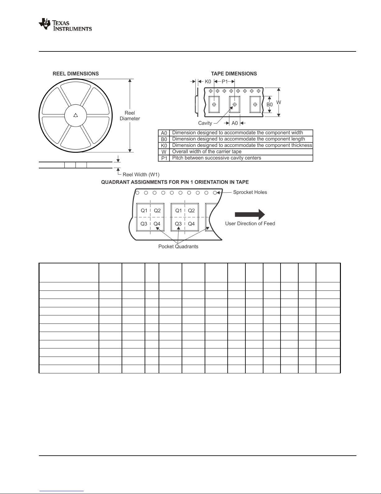
PACKAGE MATERIALS INFORMATION
www.ti.com 3-Nov-2018
TAPE AND REEL INFORMATION
*All dimensions are nominal
Device Package
MSP430G2444IDA38R TSSOP DA 38 2000 330.0 24.4 8.6 13.0 1.8 12.0 24.0 Q1
MSP430G2444IRHA40R VQFN RHA 40 2500 330.0 16.4 6.3 6.3 1.1 12.0 16.0 Q2
MSP430G2444IRHA40T VQFN RHA 40 250 180.0 16.4 6.3 6.3 1.1 12.0 16.0 Q2
MSP430G2544IDA38R TSSOP DA 38 2000 330.0 24.4 8.6 13.0 1.8 12.0 24.0 Q1
MSP430G2544IRHA40R VQFN RHA 40 2500 330.0 16.4 6.3 6.3 1.1 12.0 16.0 Q2
MSP430G2544IRHA40R VQFN RHA 40 2500 330.0 16.4 6.3 6.3 1.1 12.0 16.0 Q2
MSP430G2544IRHA40T VQFN RHA 40 250 180.0 16.4 6.3 6.3 1.1 12.0 16.0 Q2
MSP430G2544IRHA40T VQFN RHA 40 250 180.0 16.4 6.3 6.3 1.1 12.0 16.0 Q2
MSP430G2744IDA38R TSSOP DA 38 2000 330.0 24.4 8.6 13.0 1.8 12.0 24.0 Q1
MSP430G2744IRHA40R VQFN RHA 40 2500 330.0 16.4 6.3 6.3 1.1 12.0 16.0 Q2
MSP430G2744IRHA40T VQFN RHA 40 250 180.0 16.4 6.3 6.3 1.1 12.0 16.0 Q2
Type
Package
Drawing
Pins SPQ Reel
Diameter
(mm)
Reel
Width
W1 (mm)
A0
(mm)B0(mm)K0(mm)P1(mm)W(mm)
Quadrant
Pin1
Pack Materials-Page 1

PACKAGE MATERIALS INFORMATION
www.ti.com 3-Nov-2018
*All dimensions are nominal
Device Package Type Package Drawing Pins SPQ Length (mm) Width (mm) Height (mm)
MSP430G2444IDA38R TSSOP DA 38 2000 367.0 367.0 45.0
MSP430G2444IRHA40R VQFN RHA 40 2500 367.0 367.0 35.0
MSP430G2444IRHA40T VQFN RHA 40 250 210.0 185.0 35.0
MSP430G2544IDA38R TSSOP DA 38 2000 367.0 367.0 45.0
MSP430G2544IRHA40R VQFN RHA 40 2500 367.0 367.0 38.0
MSP430G2544IRHA40R VQFN RHA 40 2500 367.0 367.0 35.0
MSP430G2544IRHA40T VQFN RHA 40 250 210.0 185.0 35.0
MSP430G2544IRHA40T VQFN RHA 40 250 210.0 185.0 35.0
MSP430G2744IDA38R TSSOP DA 38 2000 367.0 367.0 45.0
MSP430G2744IRHA40R VQFN RHA 40 2500 367.0 367.0 35.0
MSP430G2744IRHA40T VQFN RHA 40 250 210.0 185.0 35.0
Pack Materials-Page 2


IMPORTANT NOTICE AND DISCLAIMER
TI PROVIDES TECHNICAL AND RELIABILITY DATA (INCLUDING DATASHEETS), DESIGN RESOURCES (INCLUDING REFERENCE
DESIGNS), APPLICATION OR OTHER DESIGN ADVICE, WEB TOOLS, SAFETY INFORMATION, AND OTHER RESOURCES “AS IS”
AND WITH ALL FAULTS, AND DISCLAIMS ALL WARRANTIES, EXPRESS AND IMPLIED, INCLUDING WITHOUT LIMITATION ANY
IMPLIED WARRANTIES OF MERCHANTABILITY, FITNESS FOR A PARTICULAR PURPOSE OR NON-INFRINGEMENT OF THIRD
PARTY INTELLECTUAL PROPERTY RIGHTS.
These resources are intended for skilled developers designing with TI products. You are solely responsible for (1) selecting the appropriate
TI products for your application, (2) designing, validating and testing your application, and (3) ensuring your application meets applicable
standards, and any other safety, security, or other requirements. These resources are subject to change without notice. TI grants you
permission to use these resources only for development of an application that uses the TI products described in the resource. Other
reproduction and display of these resources is prohibited. No license is granted to any other TI intellectual property right or to any third
party intellectual property right. TI disclaims responsibility for, and you will fully indemnify TI and its representatives against, any claims,
damages, costs, losses, and liabilities arising out of your use of these resources.
TI’s products are provided subject to TI’s Terms of Sale (www.ti.com/legal/termsofsale.html) or other applicable terms available either on
ti.com or provided in conjunction with such TI products. TI’s provision of these resources does not expand or otherwise alter TI’s applicable
warranties or warranty disclaimers for TI products.
Mailing Address: Texas Instruments, Post Office Box 655303, Dallas, Texas 75265
Copyright © 2018, Texas Instruments Incorporated
 Loading...