

LT1013, LT1013A, LT1013D, LT1013Y
DUAL PRECISION OPERATIONAL AMPLIFIERS
SLOS018B – MA Y 1988 – REVISED OCT OBER 1996
D
Single-Supply Operation:
Input Voltage Range Extends to Ground
Output Swings to Ground While Sinking
Current
D
Input Offset Voltage
150 µV Max at 25°C for LT1013A
D
Offset Voltage Temperature Coefficient
2.5 µV/°C Max for LT1013A
D
Input Offset Current
0.8 nA Max at 25°C for LT1013A
D
High Gain...1.5 V/µV Min ( R
0.8 V/µV Min ( R
D
Low Supply Current...0.5 mA Max at
T
= 25°C for LT1013A
A
D
Low Peak-to-Peak Noise Voltage
= 600 kΩ) for LT1013A
L
= 2 kΩ),
L
0.55 µV Typ
D
Low Current Noise...0.07 pA/√HZ Typ
description
The LT1013 is a dual precision operational
amplifier featuring low offset voltage temperature
coefficient, high gain, low supply current, and low
noise.
The LT1013 can be operated from a single 5-V
power supply; the common-mode input voltage
range includes ground, and the output can also
swing to within a few millivolts of ground.
Crossover distortion is eliminated. The LT1013
can be operated with both dual ±15-V and single
5-V supplies.
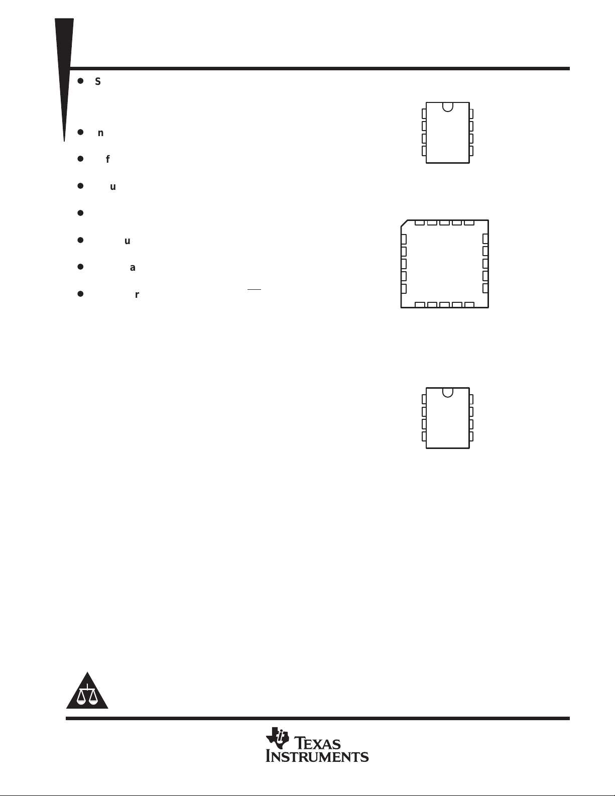
D PACKAGE
(TOP VIEW)
1IN+
V
CC–
2IN+
2IN–
NC
1IN–
NC
1IN+
NC
NC – No internal connection
1OUT
1IN–
1IN+
V
CC–
1
2
3
4
FK PACKAGE
(TOP VIEW)
NC
3 2 1 20 19
4
5
6
7
8
910111213
NC
JG OR P PACKAGE
(TOP VIEW)
1
2
3
4
1OUT
NCNCNC
NC
CC –
V
8
7
6
5
CC±
V
2IN+
8
7
6
5
1IN–
1OUT
V
CC+
2OUT
18
17
16
15
14
V
CC+
2OUT
2IN–
2IN+
NC
2OUT
NC
2IN–
NC
The L T1013C and LT1013AC, and L T1013D are characterized for operation from 0°C to 70°C. The L T1013I and
L T1013AI, and L T1013DI are characterized for operation from –40°C to 105°C. The L T1013M and L T1013AM,
and LT1013DM are characterized for operation over the full military temperature range of –55°C to 125°C.
Please be aware that an important notice concerning availability, standard warranty, and use in critical applications of
Texas Instruments semiconductor products and disclaimers thereto appears at the end of this data sheet.
PRODUCTION DATA information is current as of publication date.
Products conform to specifications per the terms of Texas Instruments
standard warranty. Production processing does not necessarily include
testing of all parameters.
POST OFFICE BOX 655303 • DALLAS, TEXAS 75265
Copyright 1996, Texas Instruments Incorporated
On products compliant to MIL-PRF-38535, all parameters are tested
unless otherwise noted. On all other products, production
processing does not necessarily include testing of all parameters.
1
LT1013, LT1013A, LT1013D, LT1013Y
VIOmax
CHIP FORM
µ
µ
µ
DUAL PRECISION OPERATIONAL AMPLIFIERS
SLOS018B – MA Y 1988 – REVISED OCT OBER 1996
AVAILABLE OPTIONS
PACKAGED DEVICES
T
A
0°C to 70°C
–40°C to 105°C
–55°C to 125°C
The D package is available taped and reeled. Add the suffix R to the device type (e.g., LT1013DDR).
AT 25°C
150 µV — — — LT1013ACP
300 µV — — — LT1013CP
800 µV LT1013DD — — LT1013DP
150 µV — — — LT1013AIP
300 µV — — — LT1013IP
800 µV LT1013DID — — LT1013DIP
150 µV — LT1013AMFK — LT1013AMP
300 µV — LT1013MFK LT1013MJG LT1013MP
800 µV LT1013DMD — LT1013DMJG LT1013DMP
SMALL OUTLINE
(D)
CHIP CARRIER
(FK)
CERAMIC DIP
(JG)
PLASTIC DIP
(P)
(Y)
LT1013Y
—
—
2
POST OFFICE BOX 655303 • DALLAS, TEXAS 75265
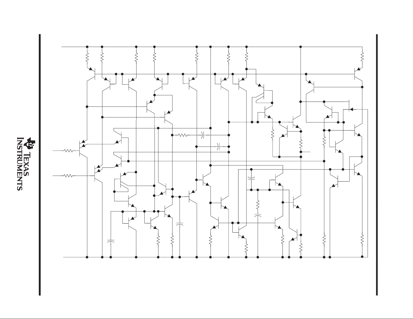
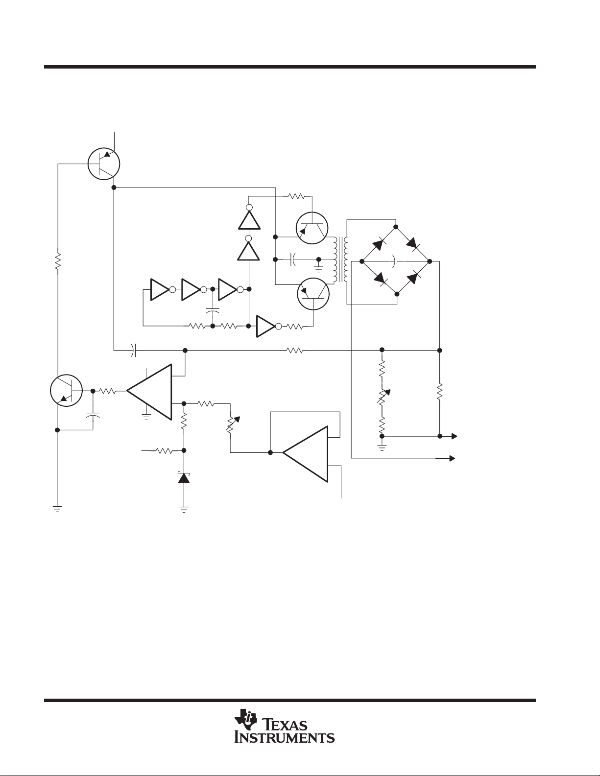
schematic (each amplifier)
V
CC+
POST OFFICE BOX 655303 DALLAS, TEXAS 75265
• 3
9 kΩ 9 kΩ 1.6 kΩ 1.6 kΩ 1.6 kΩ 100 Ω 1 kΩ
Q5
Q1
400 Ω
IN–
Q21
400 Ω
IN+
V
CC–
Component values are nominal.
Q2
Q22
Q3
Q27
Q28
Q12
Q11
Q9
75 pF 5 kΩ 5 kΩ
Q29
Q7
Q4
Q8
3.9 kΩ
10 pF
21 pF
Q10
2 kΩ
Q18
Q17
2.5 pF
Q19
1.3 kΩ
Q32Q15Q14Q16Q13Q6
Q20
Q30
2.4 kΩ
4 pF
2 kΩ
10 pF
Q25
2 kΩ
Q26
Q31
Q23
18 Ω
Q24
Q33
Q34
Q35
30 Ω
14 kΩ
OUT
42 kΩ
800 Ω
Q36
J1
Q37
Q41
Q38
DUAL PRECISION OPERATIONAL AMPLIFIERS
Q39
Q40
LT1013, LT1013A, LT1013D, LT1013Y
SLOS018B – MAY 1988 – REVISED OCTOBER 1996
600 Ω
LT1013, LT1013A, LT1013D, LT1013Y
DUAL PRECISION OPERATIONAL AMPLIFIERS
SLOS018B – MA Y 1988 – REVISED OCT OBER 1996
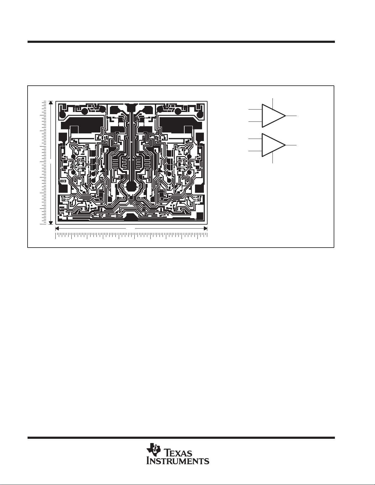
LT1013Y chip information
This chip, when properly assembled, displays characteristics similar to the LT1013. Thermal compression or
ultrasonic bonding may be used on the doped-aluminum bonding pads. Chips may be mounted with conductive
epoxy or a gold-silicon preform.
79
(2)
(3)
BONDING PAD ASSIGNMENTS
(8)
(1)
(7)
(4)
96
(6)
(5)
IN+
IN–
2 IN+
2IN–
CHIP THICKNESS: 15 TYPICAL
BONDING PADS: 4 × 4 MINIMUM
TJmax = 150°C
TOLERANCES ARE ±10%.
ALL DIMENSIONS ARE IN MILS.
PIN (4) IS INTERNALLY CONNECTED
TO BACKSIDE OF CHIP.
(3)
(2)
(5)
(6)
V
CC+
(8)
+
–
+
–
V
CC–
(4)
(1)
(7)
1OUT
2OUT
absolute maximum ratings over operating free-air temperature range (unless otherwise noted)
Supply voltage, V
Supply voltage, V
(see Note 1) 22 V. . . . . . . . . . . . . . . . . . . . . . . . . . . . . . . . . . . . . . . . . . . . . . . . . . . . . . . . . . .
CC+
(see Note 1) –22 V. . . . . . . . . . . . . . . . . . . . . . . . . . . . . . . . . . . . . . . . . . . . . . . . . . . . . . . . . .
CC–
Differential input voltage (see Note 2) ±30 V. . . . . . . . . . . . . . . . . . . . . . . . . . . . . . . . . . . . . . . . . . . . . . . . . . . . . . . .
Input voltage range, V
(any input, see Note 1) V
I
. . . . . . . . . . . . . . . . . . . . . . . . . . . . . . . . . . .
Duration of short-circuit current at (or below) 25°C (see Note 3) unlimited. . . . . . . . . . . . . . . . . . . . . . . . . . . . . .
Operating free-air temperature range, T
: LT1013C, LT1013AC, LT1013D –0 °C to 70°C. . . . . . . . . . . . . .
A
LT1013I, LT1013AI, LT1013DI –40°C to 105°C. . . . . . . . . . . . . . .
LT1013M, LT1013AM, LT1013DM –55 °C to 125°C. . . . . . . . . .
Storage temperature range –65 °C to 150°C. . . . . . . . . . . . . . . . . . . . . . . . . . . . . . . . . . . . . . . . . . . . . . . . . . . . . . .
Lead temperature 1.6 mm (1/16 inch) from case for 10 seconds: D or P package 260°C. . . . . . . . . . . . . . . . .
Case temperature for 60 seconds: FK package 260°C. . . . . . . . . . . . . . . . . . . . . . . . . . . . . . . . . . . . . . . . . . . . . .
Lead temperature 1.6 mm (1/16 inch) from case for 10 seconds: JG package 300°C. . . . . . . . . . . . . . . . . . . .
NOTES: 1. All voltage values, except differential voltages, are with respect to the midpoint between V
2. Differential voltages are at IN+ with respect to IN–.
3. The output may be shorted to either supply.
CC+
and V
CC–
CC–
.
–5 V to V
CC+
4
POST OFFICE BOX 655303 • DALLAS, TEXAS 75265
POST OFFICE BOX 655303 DALLAS, TEXAS 75265
PARAMETER
TEST CONDITIONS
T
†
UNIT
VIOInput offset voltage
R
Ω
V
Full range
0.4
2.5
0.320.7
5µV/°C
IIOInput offset current
nA
IIBInput bias current
nA
V
Common-mode input voltage range
V
g
VOMMaximum peak output voltage swing
R
kΩ
V
am lification
V
±10 V
R
2 kΩ
CMRR
Common-mode rejection ratio
dB
k
SVR
ygj
V
±18 V
dB
ICCSupply current per amplifier
mA
• 5
electrical characteristics at specified free-air temperature, V
A
p
α
VIO
ICR
A
r
id
r
ic
†
Full range is 0°C to 70°C.
‡
All typical values are at TA = 25°C.
Temperature coefficient of input
offset voltage
Long-term drift of input offset voltage 25°C 0.5 0.4 0.5 µV/mo
p
p
p
p
Large-signal differential voltage
VD
p
Supply-voltage rejection ratio
(∆VCC/∆VIO)
Channel separation VO = ±10 V, RL = 2 kΩ 25°C 120 137 123 140 120 137 dB
Differential input resistance 25°C 70 300 100 400 70 300 MΩ
Common-mode input resistance 25°C 4 5 4 GΩ
pp
p
= 50
S
p
p
= 2
L
VO = ±10 V, RL = 600 Ω 25°C
,
O =
VIC = –15 V to 13.5 V 25°C
VIC = –14.9 V to 13 V Full range
= ±2 V to
CC+
=
L
25°C
Full range 400 240 1000
25°C
Full range 2.8 1.5 2.8
25°C
Full range –38 –25 –38
25°C
Full range
25°C
Full range
25°C
Full range
25°C
Full range
25°C
Full range 0.7 0.55 0.6
= ±15 V, VIC = 0 (unless otherwise noted)
CC±
LT1013C LT1013AC LT1013DC
‡
60
0.2
–15
0.35
MAX
300
1.5
–30
0.55
MIN TYP
MIN TYP
–15 –15.3 –15 –15.3 –15 –15.3
to to to to to to
13.5 13.8 13.5 13.8 13.5 13.8
–15 –15 –15
to to to
13 13 13
±12.5 ±14 ±13 ±14 ±12.5 ±14
±12 ±12.5 ±12
0.5 0.2 0.8 2.5 0.5 2
1.2 7 1.5 8 1.2 7
0.7 1 0.7
97 114 100 117 97 114
94 98 94
100 117 103 120 100 117
97 101 97
40
0.15
–12
0.35
‡
MAX
150
0.8
–20
0.5
MIN TYP
–15
0.35
200
0.2
‡
MAX
800
µ
°
1.5
–30
DUAL PRECISION OPERATIONAL AMPLIFIERS
V/µV
LT1013, LT1013A, LT1013D, LT1013Y
SLOS018B – MAY 1988 – REVISED OCTOBER 1996
0.55
T
l
R
l
D
7
11
94
6
PARAMETER
TEST CONDITIONS
T
†
UNIT
VIOInput offset voltage
R
Ω
V
IIOInput offset current
nA
IIBInput bias current
nA
0to0.3to0to0.3to0to0.3
V
g
V
0to0to0
g
,
mV
swing
g,
A
gg
V
5 mV to 4 V
R
500 Ω
25°C111V/µV
ICCSupply current per amplifier
mA
VnEquivalent input noise voltage
V/√H
POST OFFICE BOX 655303 DALLAS, TEXAS 75265
•
electrical characteristics at specified free-air temperature, V
p
p
p
ICR
V
OM
†
Full range is –0°C to 70°C.
Common-mode input voltage
range
Maximum-peak output voltage
Large-signal differential
VD
voltage amplification
pp
= 50
S
Output low, No load 25°C 15 25 15 25 15 25
Output low,
RL = 600 Ω to GND
Output low, I
Output high, No load 25°C 4 4.4 4 4.4 4 4.4
Output high,
RL = 600 Ω to GND
=
O
p
p
= 1 mA 25°C 220 350 220 350 220 350
sink
,
=
L
25°C 90 450 60 250 250 950
Full range 570 350 1200
25°C 0.3 2 0.2 1.3 0.3 2
Full range 6 3.5 6
25°C –18 –50 –15 –35 –18 –50
Full range –90 –55 –90
25°C
Full range
25°C 5 10 5 10 5 10
Full range 13 13 13
25°C 3.4 4 3.4 4 3.4 4
Full range 3.2 3.3 3.2
25°C 0.32 0.5 0.31 0.45 0.32 0.5
Full range 0.55 0.5 0.55
A
°
= 5 V , V
CC+
LT1013C LT1013AC LT1013DC
MIN TYP MAX MIN TYP MAX MIN TYP MAX
0 –0.3 0 –0.3 0 0.3
3.5 3.8 3.5 3.8 3.5 3.8
0 0 0
3 3 3
= 0, VO = 1.4 V , VIC = 0 (unless otherwise noted)
CC–
LT1013, LT1013A, LT1013D, LT1013Y
DUAL PRECISION OPERATIONAL AMPLIFIERS
SLOS018B – MAY 1988 – REVISED OCTOBER 1996
emp
ate
µ
e
ease
ate:
to
to
V
–
–
operating characteristics, V
SR Slew rate 0.2 0.4 V/µs
V
N(PP)
I
n
=±15 V, VIC = 0, TA = 25°C
CC±
PARAMETER TEST CONDITIONS MIN TYP MAX UNIT
p
Peak-to-peak equivalent input noise voltage f = 0.1 Hz to 10 Hz 0.55 µV
Equivalent input noise current f = 10 Hz 0.07 pA/√Hz
f = 10 Hz 24
f = 1 kHz 22
n
z
POST OFFICE BOX 655303 DALLAS, TEXAS 75265
PARAMETER
TEST CONDITIONS
T
†
UNIT
VIOInput offset voltage
R
Ω
V
α
VIO
Full range
0.4
2.5
0.320.7
5µV/°C
g
25°C
0.5
0.4
0.5µV/mo
IIOInput offset current
nA
IIBInput bias current
nA
V
Common-mode input voltage range
V
g
V
g
R
kΩ
V
am lification
V
±10 V
R
2 kΩ
CMRR
dB
k
SVR
ygj
V
±18 V
dB
ICCSupply current per amplifier
mA
• 7
electrical characteristics at specified free-air temperature, V
A
p
Temperature coefficient of input
offset voltage
Long-term drift of input offset
voltage
p
p
ICR
OM
A
r
id
r
ic
†
Full range is –40°C to 105°C.
‡
All typical values are at TA = 25°C.
Maximum peak output voltage
swing
Large-signal differential voltage
VD
p
Common-mode
rejection ratio
Supply-voltage rejection ratio
(∆VCC/∆VIO)
Channel separation VO = ±10 V, RL = 2 kΩ 25°C 120 137 123 140 120 137 dB
Differential input resistance 25°C 70 300 100 400 70 300 MΩ
Common-mode input resistance 25°C 4 5 4 GΩ
pp
p
p
= 50
S
= 2
L
VO = ±10 V, RL = 600 Ω 25°C
,
=
O
VIC = –15 V to 13.5 V 25°C
VIC = –14.9 V to 13 V
= ±2 V to
CC±
p
=
L
25°C
Full range 550 300 1000
°
25°C
Full range 2.8 1.5 2.8
25°C
Full range –38 –25 –38
25°C
Full range
25°C
Full range
25°C
Full range
Full range
25°C
Full range
25°C
Full range 0.7 0.55 0.6
= ±15 V, VIC = 0 (unless otherwise noted)
CC±
LT1013I LT1013AI LT1013DI
‡
60
0.2
–15
0.35
MAX
300
1.5
–30
0.55
MIN TYP
MIN TYP
–15 –15.3 –15 –15.3 –15 –15.3
to to to to to to
13.5 13.8 13.5 13.8 13.5 13.8
–15 –15 –15
to to to
13 13 13
±12.5 ±14 ±13 ±14 ±12.5 ±14
±12 ±12.5 ±12
0.5 0.2 0.8 2.5 0.5 2
1.2 7 1.5 8 1.2 7
0.7 1 0.7
97 114 100 117 97 114
94 97 94
100 117 103 120 100 117
97 101 97
40
0.15
–12
0.35
‡
MAX
150
0.8
–20
0.5
MIN TYP
200
–15
0.35
0.2
‡
MAX
800
µ
°
1.5
–30
DUAL PRECISION OPERATIONAL AMPLIFIERS
V/µV
LT1013, LT1013A, LT1013D, LT1013Y
SLOS018B – MAY 1988 – REVISED OCTOBER 1996
0.55

T
l
R
l
D
7
11
94
8
PARAMETER
TEST CONDITIONS
T
†
UNIT
VIOInput offset voltage
R
Ω
V
IIOInput offset current
nA
IIBInput bias current
nA
0to0.3to0to0.3to0to0.3
V
g
V
0to0to0
g
,
mV
swing
g,
A
gg
V
5 mV to 4 V
R
500 Ω
25°C111V/µV
ICCSupply current per amplifier
mA
VnEquivalent input noise voltage
V/√H
POST OFFICE BOX 655303 DALLAS, TEXAS 75265
•
electrical characteristics at specified free-air temperature, V
p
p
p
ICR
V
OM
†
Full range is –40°C to 105°C.
Common-mode input voltage
range
Maximum-peak output voltage
Large-signal differential
VD
voltage amplification
pp
= 50
S
Output low, No load 25°C 15 25 15 25 15 25
Output low,
RL = 600 Ω to GND
Output low, I
Output high, No load 25°C 4 4.4 4 4.4 4 4.4
Output high,
RL = 600 Ω to GND
=
O
p
p
= 1 mA 25°C 220 350 220 350 220 350
sink
,
=
L
25°C 90 450 60 250 250 950
Full range 570 350 1200
25°C 0.3 2 0.2 1.3 0.3 2
Full range 6 3.5 6
25°C –18 –50 –15 –35 –18 –50
Full range –90 –55 –90
25°C
Full range
25°C 5 10 5 10 5 10
Full range 13 13 13
25°C 3.4 4 3.4 4 3.4 4 V
Full range 3.2 3.3 3.2
25°C 0.32 0.5 0.31 0.45 0.32 0.5
Full range 0.55 0.5 0.55
A
°
= 5 V , V
CC+
LT1013I LT1013AI LT1013DI
MIN TYP MAX MIN TYP MAX MIN TYP MAX
0 –0.3 0 –0.3 0 0.3
3.5 3.8 3.5 3.8 3.5 3.8
0 0 0
3 3 3
CC–
= 0, V
= 1.4 V , VIC = 0 (unless otherwise noted)
O
LT1013, LT1013A, LT1013D, LT1013Y
DUAL PRECISION OPERATIONAL AMPLIFIERS
SLOS018B – MAY 1988 – REVISED OCTOBER 1996
emp
ate
µ
e
ease
ate:
to
to
–
–
operating characteristics, V
SR Slew rate 0.2 0.4 V/µs
V
N(PP)
I
n
= ±15 V, VIC = 0, TA = 25°C
CC±
PARAMETER TEST CONDITIONS MIN TYP MAX UNIT
p
Peak-to-peak equivalent input noise voltage f = 0.1 Hz to 10 Hz 0.55 µV
Equivalent input noise current f = 10 Hz 0.07 pA/√Hz
f = 10 Hz 24
f = 1 kHz 22
n
z

POST OFFICE BOX 655303 DALLAS, TEXAS 75265
PARAMETER
TEST CONDITIONS
T
†
UNIT
VIOInput offset voltage
R
Ω
V
α
VIO
Full range
0.5
2.5∗0.4
2∗0.5
2.5
∗
V/°C
IIOInput offset current
nA
IIBInput bias current
nA
15to15.3to15to15.3to15to15.3
V
Common-mode input voltage range
V
14.9to14.9to14.9
g
VOMMaximum peak output voltage swing
R
kΩ
V
am lification
V
10 V
R
2 kΩ
CMRR
Common-mode rejection ratio
dB
k
ygj
V
±18 V
dB
ICCSupply current per amplifier
mA
• 9
electrical characteristics at specified free-air temperature, V
A
p
Temperature coefficient of input offset
voltage
Long-term drift of input offset voltage 25°C 0.5 0.4 0.5 µV/mo
p
p
ICR
A
SVR
r
id
r
ic
∗
On products compliant to MIL-PRF-38535, Class B, this parameter is not production tested.
†
Full range is –55°C to 125°C.
‡
All typical values are at TA = 25°C.
Large-signal differential voltage
VD
p
Supply-voltage rejection ratio
(∆VCC/∆VIO)
Channel separation VO = ±10 V, RL = 2 kΩ 25°C 120 137 123 140 120 137 dB
Differential input resistance 25°C 70 300 100 400 70 300 MΩ
Common-mode input resistance 25°C 4 5 4 GΩ
pp
p
p
p
p
p
= 50
S
= 2
L
VO = ±10 V, RL = 600 Ω 25°C 0.5 2 0.8 2.5 0.5 2
= +
O
VIC = –15 V to 13.5 V 25°C 97 117 100 117 97 114
VIC = –14.9 V to 13 V Full range 94 97 94
CC±
,
= ±2 V to
=
L
25°C 60 300 40 150 200 800
Full range 550 300 1000
25°C 0.2 1.5 0.15 0.8 0.2 1.5
Full range 5 2.5 5
25°C –15 –30 –12 –20 –15 –30
Full range –45 –30 –45
25°C
Full range
25°C ±12.5 ±14 ±13 ±14 ±12.5 ±14
Full range ±11.5 ±12 ±11.5
25°C 1.2 7 1.5 8 1.2 7
Full range 0.25 0.5 0.25
25°C 100 117 103 120 100 117
Full range 97 100 97
25°C 0.35 0.55 0.35 0.5 0.35 0.55
Full range 0.7 0.6 0.7
= ±15 V, VIC = 0 (unless otherwise noted)
CC±
LT1013M LT1013AM LT1013DM
MIN TYP‡MAX MIN TYP‡MAX MIN TYP‡MAX
∗
–15 –15.3 –15 –15.3 –15 –15.3
13.5 13.8 13.5 13.8 13.5 13.8
–14.9 –14.9 –14.9
13 13 13
∗
to
µ
∗
°
µ
to
DUAL PRECISION OPERATIONAL AMPLIFIERS
V/µV
LT1013, LT1013A, LT1013D, LT1013Y
SLOS018B – MAY 1988 – REVISED OCTOBER 1996

T
l
R
l
D
7
11
94
10
PARAMETER
TEST CONDITIONS
T
†
UNIT
R
Ω
IIOInput offset current
nA
IIBInput bias current
nA
0to0.3to0to0.3to0to0.3
V
g
V
0to0to0
g
,
mV
swing
g,
A
gg
V
5 mV to 4 V
R
500 Ω
25°C11
1
A
ICCSupply current per amplifier
VnEquivalent input noise voltage
V/√H
POST OFFICE BOX 655303 DALLAS, TEXAS 75265
•
electrical characteristics at specified free-air temperature, V
25°C 90 450 60 250 250 950
Full range 400 1500 250 900 800 2000 µV
25°C 0.3 2 0.2 1.3 0.3 2
Full range 10 6 10
25°C –18 –50 –15 –35 –18 –50
Full range –120 –80 –120
25°C
Full range
25°C 5 10 5 10 5 10
Full range 18 15 18
25°C 3.4 4 3.4 4 3.4 4
Full range 3.1 3.2 3.1
25°C 0.32 0.5 0.31 0.45 0.32 0.5
Full range 0.65 0.55 0.65
V
IO
ICR
V
OM
†
Full range is –55°C to 125°C.
Input offset voltage
p
p
Common-mode input voltage
range
Maximum-peak output voltage
Large-signal differential
VD
voltage amplification
pp
= 50
S
RS = 50 Ω, VIC = 0.1 V 125°C 200 750 120 450 560 1200
Output low, No load 25°C 15 25 15 25 15 25
Output low,
RL = 600 Ω to GND
Output low, I
Output high, No load 25°C 4 4.4 4 4.4 4 4.4
Output high,
RL = 600 Ω to GND
=
O
p
p
= 1 mA 25°C 220 350 220 350 220 350
sink
,
=
L
A
°
= 5 V , V
CC+
LT1013M LT1013AM LT1013DM
MIN TYP MAX MIN TYP MAX MIN TYP MAX
0 –0.3 0 –0.3 0 –0.3
3.5 3.8 3.5 3.8 3.5 3.8
0 0 0
3 3 3
CC –
= 0, V
= 1.4 V , VIC = 0 (unless otherwise noted)
O
LT1013, LT1013A, LT1013D, LT1013Y
DUAL PRECISION OPERATIONAL AMPLIFIERS
SLOS018B – MAY 1988 – REVISED OCTOBER 1996
emp
ate
e
ease
ate:
to
to
V/µV
m
–
–
operating characteristics, V
SR Slew rate 0.2 0.4 V/µs
V
N(PP)
I
n
= ±15 V, VIC = 0, TA = 25°C
CC±
PARAMETER TEST CONDITIONS MIN TYP MAX UNIT
p
Peak-to-peak equivalent input noise voltage f = 0.1 Hz to 10 Hz 0.55 µV
Equivalent input noise current f = 10 Hz 0.07 pA/√Hz
f = 10 Hz 24
f = 1 kHz 22
n
z

PARAMETER
TEST CONDITIONS
UNIT
0to0.3
ICR
gg
V
PARAMETER
TEST CONDITIONS
UNIT
15to15.3
ICR
gg
AVDLarge-signal differential voltage amplification
V
±10 V
dB
PARAMETER
TEST CONDITIONS
UNIT
VnEquivalent input noise voltage
V/√H
LT1013, LT1013A, LT1013D, LT1013Y
DUAL PRECISION OPERATIONAL AMPLIFIERS
SLOS018B – MA Y 1988 – REVISED OCT OBER 1996
electrical characteristics at V
CC+
= 5 V, V
= 0, VO = 1.4 V, V
CC–
= 0, TA= 25°C (unless otherwise
IC
noted)
LT1013Y
MIN TYP MAX
V
I
IO
I
IB
V
V
A
VD
I
CC
electrical characteristics at V
V
IO
I
IO
I
IB
V
ICR
V
OM
CMRR Common-mode rejection ratio VIC = –15 V to 13.5 V 97 114
k
SVR
r
id
r
ic
I
CC
Input offset voltage RS = 50 Ω 250 950 µV
IO
Input offset current 0.3 2 nA
Input bias current –18 –50 nA
Common-mode input voltage range
ICR
Output low, No load 15 25
Output low, RL = 600 Ω to GND 5 10
Maximum peak output voltage swing
OM
Large-signal differential voltage amplification VO = 5 mV to 4 V, RL = 500 Ω 1 V/µV
Supply current per amplifier 0.32 0.5 mA
= ±15 V, V
CC+
Input offset voltage RS = 50 Ω 200 800 µV
Long-term drift of input offset voltage 0.5 µV/mo
Input offset current 0.2 1.5 nA
Input bias current –15 –30 nA
Common-mode input voltage range
Maximum peak output voltage swing RL = 2 kΩ ±12.5 ±14 V
p
Supply-voltage rejection ratio (∆VCC /∆VIO) V
Channel separation VO = ±10 V, RL = 2 Ω 120 137 dB
Differential input resistance 70 300 MΩ
Common-mode input resistance 4 GΩ
Supply current per amplifier 0.35 0.55 mA
Output low, I
Output high, No load 4 4.4
Output high, RL = 600 Ω to GND 3.4 4
IC
= 0, T
= 25°C (unless otherwise noted)
A
=
O
CC±
= 1 mA 220 350
sink
RL = 600 Ω 0.5 2 V/µV
,
RL = 2 Ω 1.2 7
= ±2 V to ±18 V 100 117 dB
0 0.3
3.5 3.8
LT1013Y
MIN TYP MAX
–15 –15.3
13.5 13.8
to
to
V
mV
V
operating characteristics, VCC± = ±15 V, V
SR Slew rate 0.2 0.4 V/µs
p
V
N(PP)
I
n
Peak-to-peak equivalent input noise voltage f = 0.1 Hz to 10 Hz 0.55 µV
Equivalent input noise current f = 10 Hz 0.07 pA/√Hz
= 0, T
IC
POST OFFICE BOX 655303 • DALLAS, TEXAS 75265
= 25°C
A
f = 10 Hz 24
f = 1 kHz 22
LT1013Y
MIN TYP MAX
n
z
11

LT1013, LT1013A, LT1013D, LT1013Y
VIOInput offset voltage
AVDDifferential voltage amplification
,
Pulse response
g
,
DUAL PRECISION OPERATIONAL AMPLIFIERS
SLOS018B – MA Y 1988 – REVISED OCT OBER 1996
TYPICAL CHARACTERISTICS
Table of Graphs
p
∆V
I
IO
I
IB
V
CMRR Common-mode rejection ratio vs Frequency 13
k
SVR
I
CC
I
OS
V
I
n
V
Change in input offset voltage vs Time 3
IO
Input offset current vs Temperature 4
Input bias current vs Temperature 5
Common-mode input voltage vs Input bias current 6
IC
p
Channel separation vs Frequency 11
Output saturation voltage vs Temperature 12
Supply voltage rejection ratio vs Frequency 14
Supply current vs Temperature 15
Short-circuit output current vs Time 16
Equivalent input noise voltage vs Frequency 17
n
Equivalent input noise current vs Frequency 17
Peak-to-peak input noise voltage vs Time 18
n(PP)
p
Phase shift vs Frequency 9
FIGURE
vs Source resistance 1
vs Temperature 2
vs Load resistance 7, 8
vs Frequency
Small signal 19, 21
Large signal
9, 10
20, 22, 23
12
POST OFFICE BOX 655303 • DALLAS, TEXAS 75265

LT1013, LT1013A, LT1013D, LT1013Y
DUAL PRECISION OPERATIONAL AMPLIFIERS
SLOS018B – MA Y 1988 – REVISED OCT OBER 1996
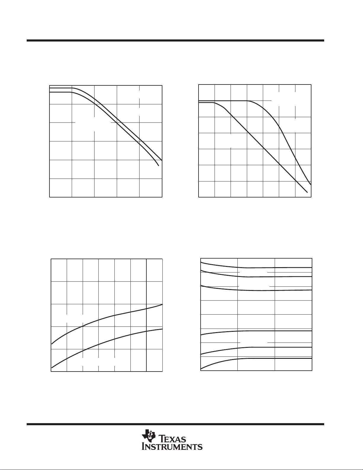
10
1
0.1
IO
VIO – Input Offset Voltage – mV
V
0.01
1 k
TYPICAL CHARACTERISTICS
INPUT OFFSET VOLTAGE
vs
SUPPLY VOLTAGE
V
= 5 V, V
CC+
TA = –55°C to 125°C
V
= ±15 V
CC±
TA = –55°C to 125°C
V
= 5 V
CC+
V
= 0
CC–
TA = 25°C
V
= ± 15V
CC±
TA = 25°C
3 k 30 k 100 k 300 k 1 M 3 M 10 M
10 k
|V
| – Supply Voltage – V
CC±
Figure 1 Figure 2
R
R
CC–
S
S
= 0
–
+
250
200
Vµ
150
100
50
0
–50
–100
IO
VIO – Input Offset Voltage – uV
V
–150
–200
–250
–50 –25
†
INPUT OFFSET VOLTAGE
OF REPRESENTITIVE UNITS
vs
FREE-AIR TEMPERATURE
V
= ±15 V
CC±
TA – Free-Air Temperature – ° C
1251007550250
Vµ
IO
XVIO – Change in Input Offset Voltage – uV∆V
WARM-UP CHANGE
IN INPUT OFFSET VOLTAGE
vs
TIME AFTER POWER-ON
5
V
= ±15 V
CC±
TA = 25°C
4
3
2
JG Package
1
0
0123
t – Time After Power-On – min
Figure 3
45
INPUT OFFSET CURRENT
FREE-AIR TEMPERATURE
1
VIC = 0
0.8
0.6
0.4
V
CC+
IO
IIO – Input Offset Current – nA
I
0.2
V
= ±15 V
CC±
0
–50 –25
TA – Free-Air Temperature – ° C
= 5 V, V
0 25 50 75 100
Figure 4
CC–
vs
V
CC±
= 0
= ±2.5 V
125
†
Data at high and low temperatures are applicable only within the rated operating free-air temperature ranges of the various devices.
POST OFFICE BOX 655303 • DALLAS, TEXAS 75265
13

LT1013, LT1013A, LT1013D, LT1013Y
DUAL PRECISION OPERATIONAL AMPLIFIERS
SLOS018B – MA Y 1988 – REVISED OCT OBER 1996
TYPICAL CHARACTERISTICS
INPUT BIAS CURRENT
vs
FREE-AIR TEMPERATURE
–30
–25
–20
–15
–10
IB
I
IIB – Input Bias Current – nA
VIC = 0
V
= 5 V, V
CC±
V
= ±15 V
CC±
–5
0
–50 –25 0 25 50 75 100 125
TA – Free-Air Temperature – ° C
CC–
= 0
V
CC±
Figure 5
= ±2.5 V
†
COMMON-MODE INPUT VOLTAGE
vs
INPUT BIAS CURRENT
15
TA = 25°C
10
5
V
= ±15 V
CC±
(left scale)
0
–5
–10
IC
V
VIC – Common-Mode Input Voltage – V
–15
0 –5 –10 –15 – 20 –25 –30
IIB – Input Bias Current – nA
V
= 5 V
CC±
V
= 0
CC–
(right scale)
Figure 6
5
4
3
2
1
0
–1
IC
V
VIC – Common-Mode Input Voltage – V
DIFFERENTIAL VOLTAGE AMPLIFICATION
vs
LOAD RESISTANCE
10
V
µV
4
1
0.4
VD
AVD – Differential Voltage Amplification – V/
A
0.1
100 400 1 k 4 k 10 k
= ±15 V
CC±
VO = ±10 V
TA = –55°C
TA = 25°C
TA = 125°C
RL – Load Resistance – Ω
Figure 7
DIFFERENTIAL VOLTAGE AMPLIFICATION
vs
LOAD RESISTANCE
10
V
µV
4
1
0.4
VD
AVD – Differential Voltage Amplification – V/A
0.1
100 400 1 k 4 k 10 k
= 5 V, V
CC±
VO = 20 mV to 3.5 V
= 0
CC–
TA = –55°C
TA = 125°C
RL – Load Resistance – Ω
TA = 25°C
Figure 8
†
Data at high and low temperatures are applicable only within the rated operating free-air temperature ranges of the various devices.
14
POST OFFICE BOX 655303 • DALLAS, TEXAS 75265

LT1013, LT1013A, LT1013D, LT1013Y
DUAL PRECISION OPERATIONAL AMPLIFIERS
SLOS018B – MA Y 1988 – REVISED OCT OBER 1996
TYPICAL CHARACTERISTICS
DIFFERENTIAL VOLTAGE AMPLIFICATION
AND PHASE SHIFT
vs
FREQUENCY
25
VIC = 0
20
15
10
A
VD
5
V
= 5 V
CC+
0
V
= 0
CC–
–5
V
–10
VD
AVD – Differential Voltage Amplification – dB
A
–15
0.01 0.3 1 3 10
CC±
V
= ±15 V
CC±
Phase Shift
= ±15 V
f – Frequency – MHz
CL = 100 pF
TA = 25°C
V
= 5 V
CC+
V
= 0
CC–
80°
100°
120°
140°
160°
180°
200°
220°
240°
†
DIFFERENTIAL VOLTAGE AMPLIFICATION
vs
FREQUENCY
140
120
100
V
= 5 V
CC+
VCC– = 0
80
60
40
20
0
VD
AVD – Differential Voltage Amplification – dB
A
–20
0.01 0.1 1 10 100 1 k 10 k 100 k 1 M 10 M
f – Frequency – Hz
V
CC±
CL = 100 pF
TA = 25°C
= ±15 V
CHANNEL SEPARATION
160
140
Limited by
120
100
Channel Separation – dB
Thermal
Interaction
80
60
10 100 1 k 10 k
f – Frequency – Hz
Figure 9
vs
FREQUENCY
V
CC±
V
I(PP)
RL = 2 kΩ
TA = 25°C
RL = 1 kΩ
Limited by
Pin-to-Pin
Capacitance
Figure 11
= ±15 V
= 20 V to 5 kHz
RL = 100 Ω
100 k 1 M
Figure 10
OUTPUT SATURATION VOLTAGE
vs
FREE-AIR TEMPERATURE
10
I
= 10 mA
sink
1
I
= 5 mA
sink
I
= 1 mA
sink
I
= 100 µA
sink
0.1
Output Saturation Voltage – V
I
= 10 µA
sink
I
= 0
sink
0.01
–50 –25 0 25 50 75 100 125
TA – Free-Air Temperature – ° C
V
V
CC+
CC–
= 5 V to 30 V
= 0
Figure 12
†
Data at high and low temperatures are applicable only within the rated operating free-air temperature ranges of the various devices.
POST OFFICE BOX 655303 • DALLAS, TEXAS 75265
15
LT1013, LT1013A, LT1013D, LT1013Y
DUAL PRECISION OPERATIONAL AMPLIFIERS
SLOS018B – MA Y 1988 – REVISED OCT OBER 1996
TYPICAL CHARACTERISTICS
COMMON-MODE REJECTION RATIO
vs
FREQUENCY
120
100
V
V
= 5 V
80
60
40
20
CMRR – Common-Mode Rejection Ratio – dB
0
10 100 1 k 10 k
CC+
V
= 0
CC–
f – Frequency – Hz
TA = 25°C
= ±15 V
CC±
100 k 1 M
†
SUPPLY VOLTAGE REJECTION RATIO
140
120
100
80
60
40
20
SVR
k
kSVR – Supply Voltage Rejection Ratio – dB
0
0.1 1 10 100 1 k
Negative
Supply
f – Frequency – Hz
vs
FREQUENCY
V
= ± 15 V
CC±
TA = 25°C
Positive
Supply
10 k 100 k 1 M
Figure 13
SUPPLY CURRENT
vs
FREE-AIR TEMPERATURE
460
Aµ
420
380
V
= ±15 V
CC±
340
– Supply Current Per Amplifier –
300
CC
I
260
–50
V
= 5 V, V
CC+
–25
0 25 50 75 100 125
TA – Free-Air Temperature – ° C
CC–
= 0
40
30
20
10
–10
–20
– Short-Circuit Output Current – mA
OS
–30
I
–40
SHORT-CIRCUIT OUTPUT CURRENT
0
01
Figure 15
Figure 14
vs
ELAPSED TIME
T
= –55°C
A
TA = 25°C
TA = 125°C
TA = 125°C
TA = 25°C
TA = –55°C
23
t – Elapsed Time – min
Figure 16
V
CC±
= ±15 V
†
Data at high and low temperatures are applicable only within the rated operating free-air temperature ranges of the various devices.
16
POST OFFICE BOX 655303 • DALLAS, TEXAS 75265
LT1013, LT1013A, LT1013D, LT1013Y
DUAL PRECISION OPERATIONAL AMPLIFIERS
SLOS018B – MA Y 1988 – REVISED OCT OBER 1996
TYPICAL CHARACTERISTICS
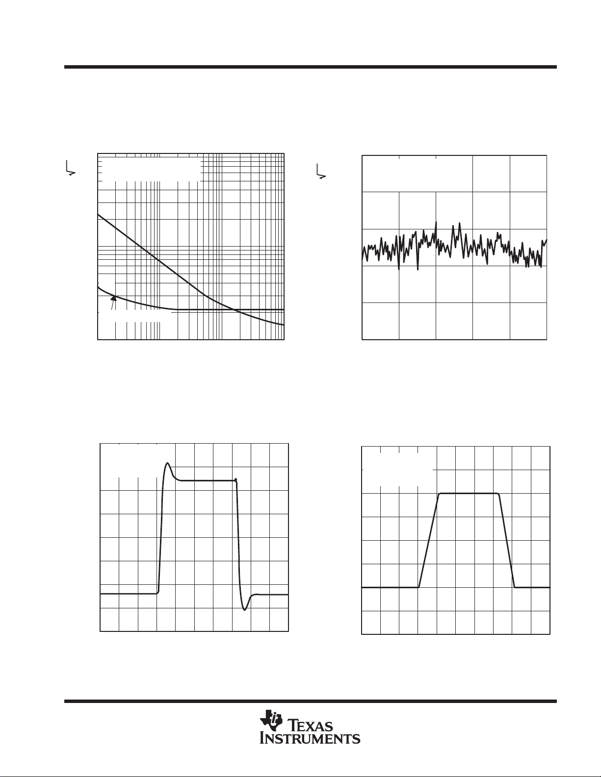
EQUIVALENT INPUT NOISE VOLTAGE
AND EQUIVALENT INPUT NOISE CURRENT
vs
FREQUENCY
1000
V
= ±2 V to ±18 V
CC±
TA = 25°C
nV/ Hz
300
I
n
1000
fA/ Hz
300
PEAK-TO-PEAK INPUT NOISE VOLTAGE
OVER A
10-SECOND PERIOD
2000
1600
1200
V
= ±2 V to ±18 V
CC±
f = 0.1 Hz to 10 Hz
TA = 25°C
100
V
n
30
1/f Corner = 2 Hz
n
V
Vn – Equivalent Input Noise Voltage – nV/Hz
10
110
f – Frequency – Hz
Figure 17
VOLTAGE-FOLLOWER
SMALL-SIGNAL
PULSE RESPONSE
80
V
= ±15 V
CC±
AV = 1
60
TA = 25°C
40
20
100
1k
100
30
10
800
N(PP)
V
VN(PP) – Noise Voltage – nV
400
n
Vn – Equivalent Input Noise Voltage – nV/Hz
V
0
0246
20
15
10
5
V
= ±15 V
CC±
AV = 1
TA = 25°C
810
t – Time – s
Figure 18
VOLTAGE-FOLLOWER
LARGE-SIGNAL
PULSE-RESPONSE
V
VO – Output Voltage – mV
0
–20
O
–40
–60
–80
46810
20
t – Time – µs
12 14
Figure 19
POST OFFICE BOX 655303 • DALLAS, TEXAS 75265
0
–5
O
V) – Output Voltage – V
V
–10
–15
–20
0 50 100 150
t – Time – µs
Figure 20
200 250 300 350
17
LT1013, LT1013A, LT1013D, LT1013Y
DUAL PRECISION OPERATIONAL AMPLIFIERS
SLOS018B – MA Y 1988 – REVISED OCT OBER 1996
TYPICAL CHARACTERISTICS
O
V
VO – Output Voltage – mV
160
140
120
100
80
60
40
20
–20
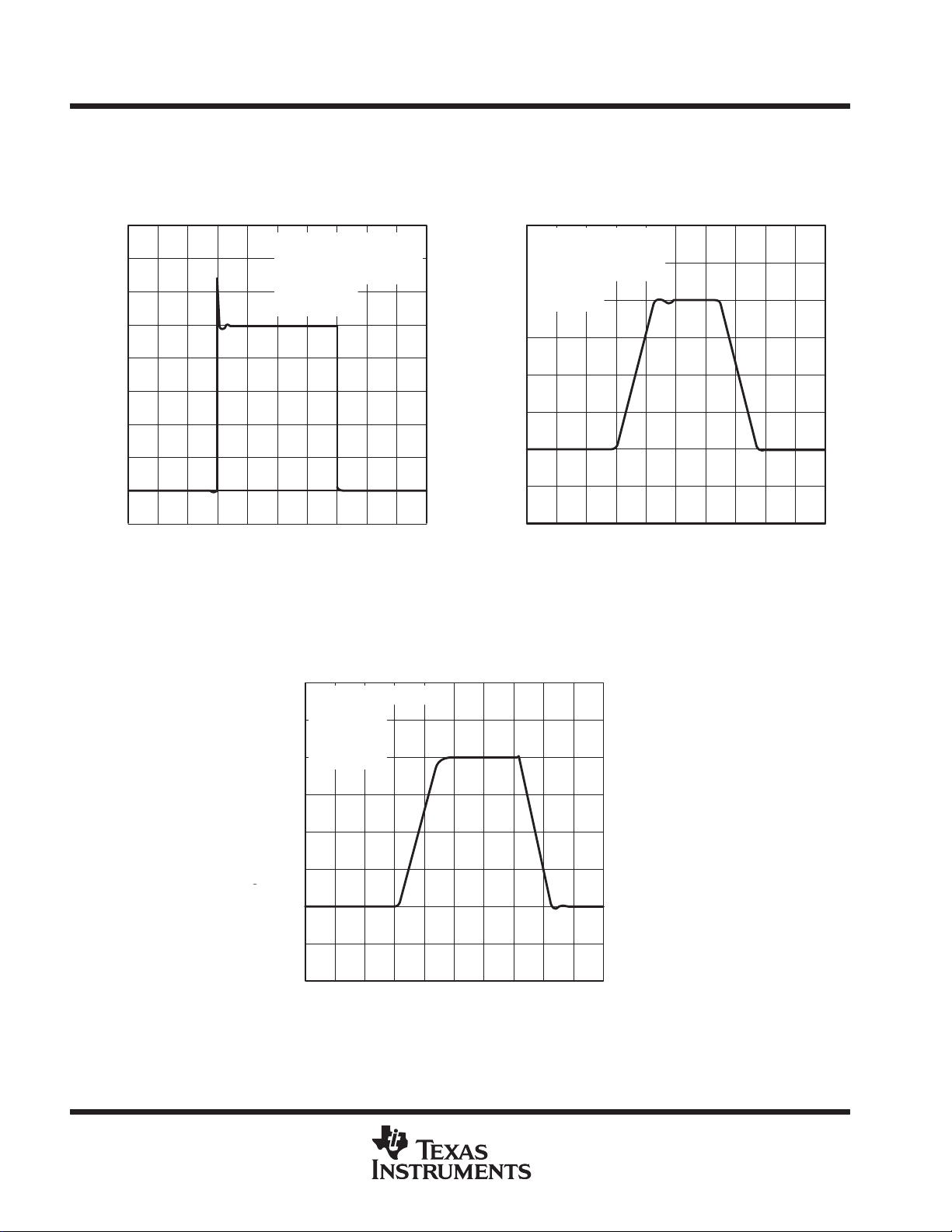
VOLTAGE-FOLLOWER
SMALL-SIGNAL
PULSE RESPONSE
6
V
V
= 5 V, V
CC+
VI = 0 to 100 mV
RL = 600 Ω to GND
AV = 1
TA = 25°C
0
0204060
t – Time – µs
80 100 120 140
CC–
= 0
O
V
VO – Output Voltage – mV
CC+
VI = 0 to 4 V
5
RL = 4.7 kΩ to 5 V
AV = 1
TA = 25°C
4
3
2
1
0
–1
–2
Figure 21
VOLTAGE-FOLLOWER
LARGE-SIGNAL
PULSE RESPONSE
= 5 V, V
= 0
CC–
0102030
t – Time – µs
Figure 22
40 50 60 70
6
5
4
3
2
1
O
V
VO – Output Voltage – V
0
–1
–2
V
= 5 V, V
CC+
VI = 0 to 4 V
RL = 0
AV = 1
TA = 25°C
VOLTAGE-FOLLOWER
LARGE-SIGNAL
PULSE RESPONSE
= 0
CC–
0102030
t – Time – µs
40 50 60 70
Figure 23
18
POST OFFICE BOX 655303 • DALLAS, TEXAS 75265

single-supply operation
LT1013, LT1013A, LT1013D, LT1013Y
DUAL PRECISION OPERATIONAL AMPLIFIERS
SLOS018B – MA Y 1988 – REVISED OCT OBER 1996
APPLICATION INFORMATION
The LT1013 is fully specified for single-supply operation (V
= 0). The common-mode input voltage range
CC–
includes ground, and the output swings to within a few millivolts of ground.
Furthermore, the LT1013 has specific circuitry that addresses the difficulties of single-supply operation, both
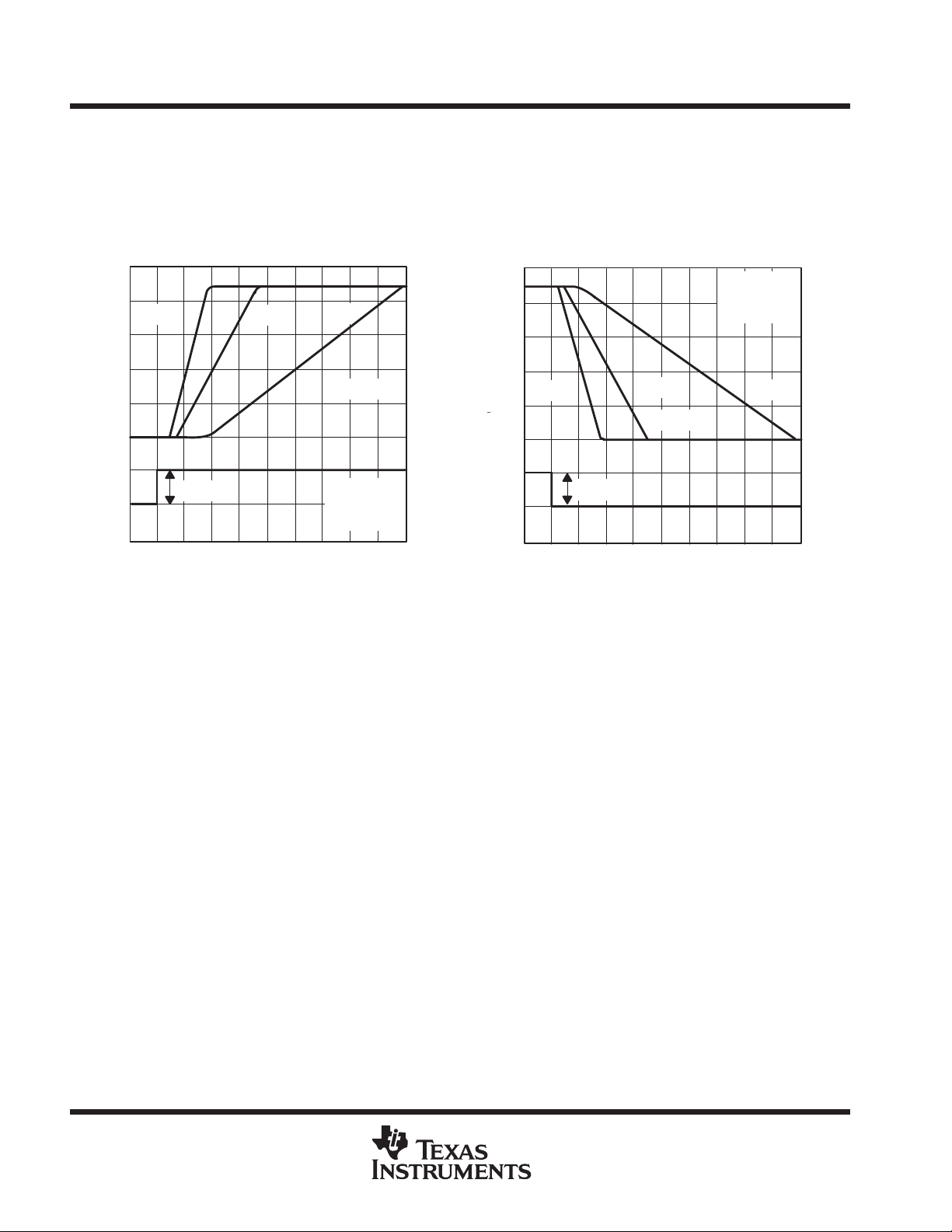
at the input and at the output. At the input, the driving signal can fall below 0 V, either inadvertently or on a
transient basis. If the input is more than a few hundred millivolts below ground, the L T1013 is designed to deal
with the following two problems that can occur:
1. On many other operational amplifiers, when the input is more than a diode drop below ground, unlimited
current will flow from the substrate (V
terminal) to the input, which can destroy the unit. On the
CC –
L T1013, the 400-Ω resistors in series with the input (see schematic) protect the device even when the
input is 5 V below ground.
2. When the input is more than 400 mV below ground (at T
= 25°C), the input stage of similar type
A
operational amplifiers saturates and phase reversal occurs at the output. This can cause lock up in
servo systems. Because of a unique phase-reversal protection circuitry (Q21, Q22, Q27, and Q28), the
LT1013 outputs do not reverse, even when the inputs are at –1.5 V (see Figure 24).
This phase-reversal protection circuitry does not function when the other operational amplifier on the L T1013
is driven hard into negative saturation at the output. Phase-reversal protection does not work on amplifier 1
when 2’s output is in negative saturation or on amplifier 2 when 1’s output is in negative saturation.
At the output, other single-supply designs either cannot swing to within 600 mV of ground or cannot sink more
than a few microproamperes while swinging to ground. The all-NPN output stage of the LT1013 maintains its
low output resistance and high gain characteristics until the output is saturated. In dual-supply operations, the
output stage is free of crossover distortion.
5
4
3
2
1
0
I(PP)
VI(PP) – Input Voltage – V
V
–1
–2
(a) V
= –1.5 V TO 4.5 V
I(PP)
Figure 24. Voltage-Follower Response With Input Exceeding
5
4
3
2
1
O
V
VO – Output Voltage – V
0
–1
(b) OUTPUT PHASE REVERSAL
EXHIBITED BY LM358
5
4
3
2
1
O
V
VO – Output Voltage – V
0
–1
the Negative Common-Mode Input Voltage Range
(c) NO PHASE REVERSAL
EXHIBITED BY LT1013
POST OFFICE BOX 655303 • DALLAS, TEXAS 75265
19
LT1013, LT1013A, LT1013D, LT1013Y
DUAL PRECISION OPERATIONAL AMPLIFIERS
SLOS018B – MA Y 1988 – REVISED OCT OBER 1996
APPLICATION INFORMATION
comparator applications
The single-supply operation of the L T1013 lends itself for use as a precision comparator with TTL-compatible
output. In systems using both operational amplifiers and comparators, the L T1013 can perform multiple duties.
Refer to Figures 25 and 26.
5
4
10 mV
3
2
1
O
V
VO – Output Voltage – V
0
Differential
Input Voltage
5 mV
100 mV
0 50 100 150 200 250 300 350 400 450
t – Time – µs
2 mV
Overdrive
V
CC+
V
CC–
TA = 25°C
Figure 25. Low-to-High-Level Output
Response for Various Input Overdrives
= 5 V
= 0
5
4
3
2
10 mV
1
O
V
VO – Output Voltage – V
0
Differential
Input Voltage
5 mV
Overdrive
100 mV
0 50 100 150 200 250 300 350 400 450
t – Time – µs
V
CC+
V
CC–
TA = 25°C
2 mV
Figure 26. High-to-Low-Level Output
Response for Various Input Overdrives
= 5 V
= 0
low-supply operation
The minimum supply voltage for proper operation of the L T1013 is 3.4 V (three Ni-Cad batteries). Typical supply
current at this voltage is 290 µA; therefore, power dissipation is only 1 mW per amplifier.
offset voltage and noise testing
The test circuit for measuring input offset voltage and its temperature coefficient is shown in Figure 30. This
circuit with supply voltages increased to ±20 V is also used as the burn-in configuration.
The peak-to-peak equivalent input noise voltage of the LT1013 is measured using the test circuit shown in
Figure 27. The frequency response of the noise tester indicates that the 0.1-Hz corner is defined by only one
zero. The test time to measure 0.1-Hz to 10-Hz noise should not exceed 10 seconds, as this time limit acts as
an additional zero to eliminate noise contribution from the frequency band below 0.1 Hz.
An input noise voltage test is recommended when measuring the noise of a large number of units. A 10-Hz input
noise voltage measurement correlates well with a 0.1-Hz peak-to-peak noise reading because both results are
determined by the white noise and the location of the 1/f corner frequency.
Current noise is measured by the circuit and formula shown in Figure 28. The noise of the source resistors is
subtracted.
20
POST OFFICE BOX 655303 • DALLAS, TEXAS 75265

APPLICATION INFORMATION
offset voltage and noise testing (continued)
0.1 µF
100 kΩ
10 Ω
+
LT1013 +
–
AVD = 50,000
2 kΩ
4.7 µF
LT1013, LT1013A, LT1013D, LT1013Y
DUAL PRECISION OPERATIONAL AMPLIFIERS
SLOS018B – MA Y 1988 – REVISED OCT OBER 1996
22 µF
Oscilloscope
Rin = 1 MΩ
LT1001
–
4.3 kΩ
2.2 µF
100 kΩ
24.3 kΩ
NOTE A: All capacitor values are for nonpolarized capacitors only.
Figure 27. 0.1-Hz to 10-Hz Peak-to-Peak Noise Test Circuit
10 kΩ
10 MΩ
100 Ω
10 MΩ
In+
†
Metal-film resistor
†
†
[V
no
10 MΩ
10 MΩ
*
(820 nV)2]
2
40 MW100
†
†
+
LT1013
–
1ń2
V
n
Figure 28. Noise-Current Test Circuit
and Formula
110 kΩ
0.1 µF
50 kΩ
(see Note A)
15 V
100 Ω
(see Note A)
50 kΩ
(see Note A)
NOTE A: Resistors must have low thermoelectric potential.
+
LT1013
–
–15 V
VO = 1000 V
IO
Figure 29. Test Circuit for VIO and αV
IO
POST OFFICE BOX 655303 • DALLAS, TEXAS 75265
21
LT1013, LT1013A, LT1013D, LT1013Y
DUAL PRECISION OPERATIONAL AMPLIFIERS
SLOS018B – MA Y 1988 – REVISED OCT OBER 1996
APPLICATION INFORMATION
typical applications
5 V
Q3
2N2905
68 Ω
Q4
2N2222
2 kΩ
100 pF
0.33 µF
5 V
LT1013
5 V
1/2
SN74HC04 (6)
0.002 µF
10 kΩ 10 kΩ 820 Ω
–
†
+
4.3 kΩ
4 kΩ
10 kΩ
LT1004
1.2 V
†
1 kΩ
4-mA
Trim
820 Ω
+
10 µF
100 kΩ
1/2
LT1013
Q1
2N2905
T1
Q2
2N2905
–
+
‡
+
10 µF
†
10 kΩ
†
10 kΩ
20-mA Trim
†
80 kΩ
1N4002 (4)
†
100 Ω
4-mA to 20-mA
To Load
2.2 kΩ MAX
†
1% film resistor. Match 10-kΩ resistors 0.05%.
‡
T1 = PICO-31080
Figure 30. 5-V 4-mA – 20-mA Current Loop Transmitter With 12-Bit Accuracy
22
IN
0 to 4 V
POST OFFICE BOX 655303 • DALLAS, TEXAS 75265

LT1013, LT1013A, LT1013D, LT1013Y
DUAL PRECISION OPERATIONAL AMPLIFIERS
SLOS018B – MA Y 1988 – REVISED OCT OBER 1996
APPLICATION INFORMATION
To Inverter
Drive
†
1% film resistor
T1
+
10 µF
5 V
5 V
1/2
LT1013
4.3 kΩ
LT1004
–
+
1.2 V
10 kΩ
4-mA
†
4 kΩ
2 kΩ
Trim
100 kΩ
†
IN
0 to 4 V
68 kΩ
301 Ω
1 kΩ
20-mA
Trim
0.1 Ω
+
1/2
LT1013
–
†
†
Figure 31. Fully Floating Modification to 4-mA – 20-mA Current Loop
Transmitter With 8-Bit Accuracy
IN+
IN–
1/2 LTC1043
6
1 µF
18
5
2
3
1 µF
15
5
6
5 V
+
1/2
LT1013
–
8
7
OUT A
4
R2
1N4002 (4)
4-mA to 20-mA
Fully Floating
R1
1/2 LTC1043
7
IN+
1 µF
13
IN–
0.01 µF
NOTE A: VIO = 150 µV, AVD = (R1/R2) + 1, CMRR = 120 dB, V
8
11
12
14
1 µF
3
2
+
1/2
LT1013
–
1
OUT B
R2
R1
ICR
= 0 to 5 V
Figure 32. 5-V Single-Supply Dual Instrumentation Amplifier
POST OFFICE BOX 655303 • DALLAS, TEXAS 75265
23

LT1013, LT1013A, LT1013D, LT1013Y
DUAL PRECISION OPERATIONAL AMPLIFIERS
SLOS018B – MA Y 1988 – REVISED OCT OBER 1996
APPLICATION INFORMATION
†
200 kΩ
5 V
2
IN–
IN+
20 kΩ
1 µF
20 kΩ
–
‡
LT1013
3
+
RG (2 kΩ typ)
‡
200 kΩ
6
‡
–
LT1013
5
+
‡
1
7
10
9
10 kΩ
10 kΩ
10 kΩ
+
LT1013
–
10 kΩ
To Input
8
Cable Shields
†
10 kΩ
†
†
13
12
–
LT1013
+
10 kΩ
5 V
4
14
OUT
11
†
5 V
†
1% film resistor. Match 10-kΩ resistors 0.05%.
‡
For high source impedances, use 2N2222 as diodes.
NOTE A: AVD = (400,000/RG) + 1
Figure 33. 5-V Precision Instrumentation Amplifier
24
POST OFFICE BOX 655303 • DALLAS, TEXAS 75265

IMPORTANT NOTICE
T exas Instruments and its subsidiaries (TI) reserve the right to make changes to their products or to discontinue
any product or service without notice, and advise customers to obtain the latest version of relevant information
to verify, before placing orders, that information being relied on is current and complete. All products are sold
subject to the terms and conditions of sale supplied at the time of order acknowledgement, including those
pertaining to warranty, patent infringement, and limitation of liability.
TI warrants performance of its semiconductor products to the specifications applicable at the time of sale in
accordance with TI’s standard warranty. Testing and other quality control techniques are utilized to the extent
TI deems necessary to support this warranty . Specific testing of all parameters of each device is not necessarily
performed, except those mandated by government requirements.
CERT AIN APPLICATIONS USING SEMICONDUCTOR PRODUCTS MA Y INVOLVE POTENTIAL RISKS OF
DEATH, PERSONAL INJURY, OR SEVERE PROPERTY OR ENVIRONMENTAL DAMAGE (“CRITICAL
APPLICATIONS”). TI SEMICONDUCTOR PRODUCTS ARE NOT DESIGNED, AUTHORIZED, OR
WARRANTED TO BE SUITABLE FOR USE IN LIFE-SUPPORT DEVICES OR SYSTEMS OR OTHER
CRITICAL APPLICA TIONS. INCLUSION OF TI PRODUCTS IN SUCH APPLICATIONS IS UNDERST OOD TO
BE FULLY AT THE CUSTOMER’S RISK.
In order to minimize risks associated with the customer’s applications, adequate design and operating
safeguards must be provided by the customer to minimize inherent or procedural hazards.
TI assumes no liability for applications assistance or customer product design. TI does not warrant or represent
that any license, either express or implied, is granted under any patent right, copyright, mask work right, or other
intellectual property right of TI covering or relating to any combination, machine, or process in which such
semiconductor products or services might be or are used. TI’s publication of information regarding any third
party’s products or services does not constitute TI’s approval, warranty or endorsement thereof.
Copyright 1998, Texas Instruments Incorporated
 Loading...