

Page 1
User's Guide
SLVUBD4A–January 2018–Revised December 2018
High Side Switch Motherboard Evaluation Module
The HSS-MOTHERBOARDEVM evaluation module is designed to evaluate the <50-mΩ Ron devices in
TI's high side switch portfolio. These devices include TPS1HA08-Q1, TPS2HB08-Q1, TPS2HB16-Q1,
TPS2HB35-Q1, and TPS2HB50-Q1. This board does not come with the devices populated but allows any
of the devices to be soldered down on the sample daughter card and used in the main motherboard. This
user's guide provides the connectors and test point description, schematic, bill of materials (BOM), and
board layout of the EVM.
NOTE: This EVM does NOT come with devices populated on the board. The user MUST order
samples separately.
Contents
1 Introduction ................................................................................................................... 2
1.1 Descriptions ......................................................................................................... 2
1.2 Applications.......................................................................................................... 2
1.3 Features.............................................................................................................. 3
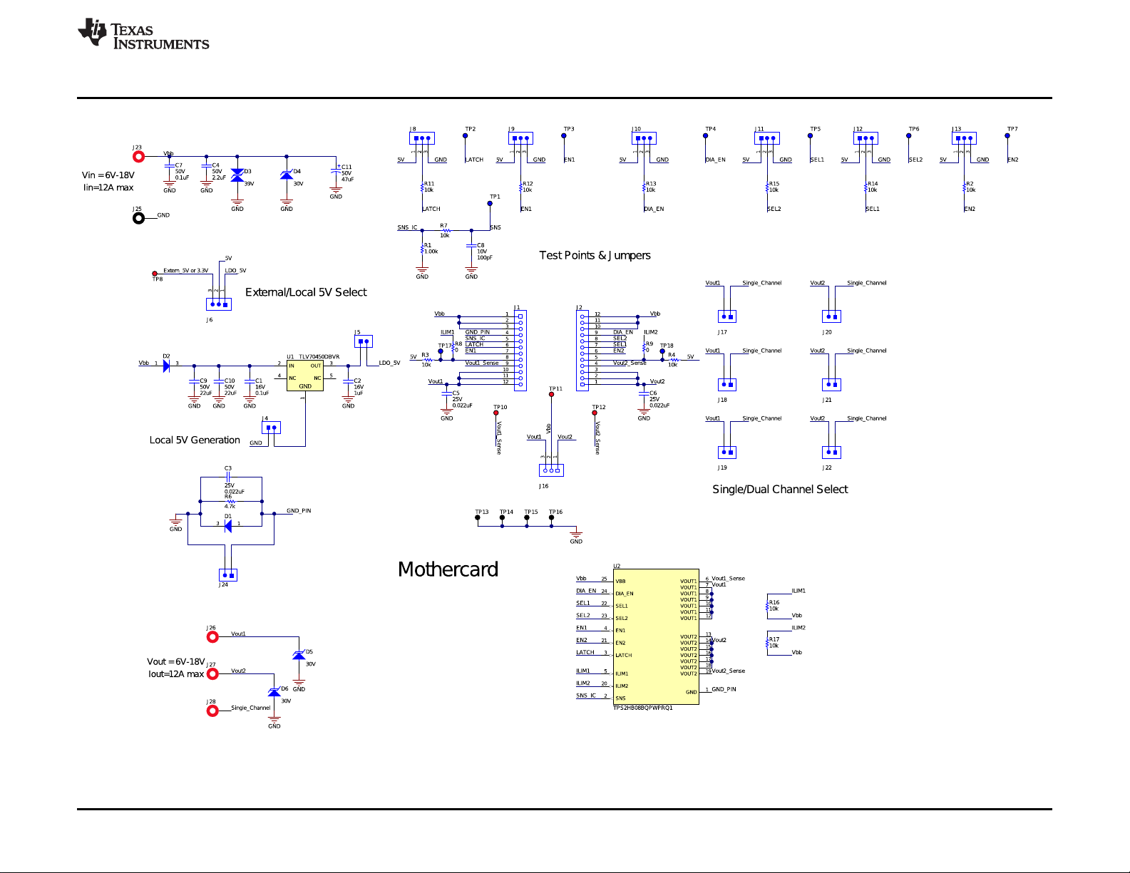
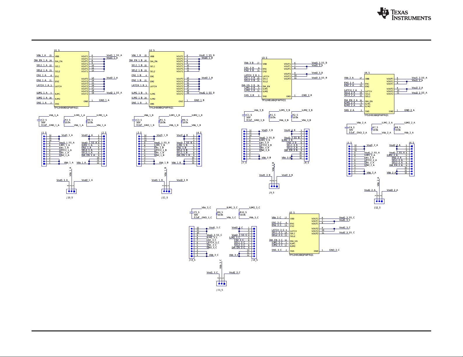
2 HSS-MOTHERBOARDEVM Schematic .................................................................................. 4
3 Connections Descriptions................................................................................................... 7
3.1 Connectors and Test Points....................................................................................... 7
3.2 Jumpers.............................................................................................................. 8
4 TPS2HB08-50EVM EVM Assembly Drawings and Layout............................................................. 9
5 Current Limit ................................................................................................................ 11
6 Current Sense .............................................................................................................. 11
7 Transient Protection........................................................................................................ 11
8 Soldering Down U2 ........................................................................................................ 11
9 Bill of Materials ............................................................................................................. 11
1 HSS-MOTHERBOARDEVM Motherboard Schematic .................................................................. 5
2 HSS-MOTHERBOARDEVM Sample Daughter Card Schematic...................................................... 6
3 HSS-MOTHERBOARDEVM Layout and Routing (Top View) ......................................................... 9
4 HSS-MOTHERBOARDEVM Layout and Routing (Bottom View).................................................... 10
1 Connector and Test Point Descriptions................................................................................... 7
2 Jumper Descriptions......................................................................................................... 8
Trademarks
All trademarks are the property of their respective owners.
SLVUBD4A–January 2018–Revised December 2018
Submit Documentation Feedback
Copyright © 2018, Texas Instruments Incorporated
List of Figures
List of Tables
High Side Switch Motherboard Evaluation Module
1
Page 2

Introduction
1 Introduction
Texas Instruments' HSS-MOTHERBOARDEVM evaluation module has a central socket for the supporting
daughtercard with the high side switch device to be populated. The EVM supports the entire singlechannel and dual channel low Ron (≤50-mΩ) high-side driver applications. The purpose of this EVM is to
facilitate evaluation of the low Ron high side switches for the diagnostic features and drive resistive,
capacitive, and inductive loads.
The EVM is a combination of a central motherboard and a row of daughterboards. The mother board has
all connectors, jumpers, and test points. The daughter board has different footprints to support the low
Ron family of TI's high side switch portfolio. The daughter board also has limiting resistors for the channel
devices (TPS2HBxx-Q1) and since the 1 channel device (TPS1HA08-Q1) has a NC pin in that location the
daughtercards will work for all of the devices.
The daughterboards have 2 different footprints: 24 pin PWP and 16 pin PWP. For installation, a single
board from the panel has to broken, a device soldered down onto the main footprint, and connected to the
motherboard.
NOTE: Caution must be taken when soldering down the device as the main power pad on the back
needs to be soldered correctly as to not affect performance. Please see PowerPAD
Thermally Enhanced Package app note for more details about the solder profile and
techniques.
The current-limiting resistors are on the bottom side of the daughterboard. They are all 10-kΩ, 0805
package. For the desired current limit value, the resistor can be replaced with different value. Also for the
single channel devices the second resistor should be depopulated.
The jumpers are not installed. Refer to Table 1 and Table 2 for installation.
www.ti.com
1.1 Descriptions
The Texas Instruments HSS-MOTHERBOARDEVM helps designers evaluate the operation and
performance of the TPS1HA08-Q1, TPS2HB08-Q1, TPS2HB16-Q1, TPS2HB35-Q1 and TPS2HB50-Q1
devices.
These devices are fully-protected high-side switches, with an integrated NMOS power FET, and charge
pump. Full diagnostics and high-accuracy current sense features enable intelligent control of the load.
The device diagnostic reporting supports load current status and device temperature on an analog sense
output pin SNS. The SNS pin sources a current proportional to the selected parameter. By adding a
pulldown resistor on the SNS pin, the developed voltage is proportional to the selected parameter as well.
The diagnostics can be disabled for multiplexing the sense pin between different devices.
1.2 Applications
The EVM is used in the following applications:
• High-side relay drivers
• High-side power switch for submodule power supply
• Bulb driver
• General resistive, inductive, and capacitive loads
• Replace electromechanical relays and fuses
2
High Side Switch Motherboard Evaluation Module
Copyright © 2018, Texas Instruments Incorporated
SLVUBD4A–January 2018–Revised December 2018
Submit Documentation Feedback
Page 3

www.ti.com
1.3 Features
The EVM supports the following features:
• Single or Dual-channel high-side power switches, tested according to AECQ100-12
• Operating voltage 3 V to 18V
• Operating temperature: –40ºC to 125ºC
• Microcontroller input control: 3.3-V and 5-V logic compatible
• High-accuracy current sense
– Analog current sense as a ratio of the load current or device temperature
• Protection:
– Reverse battery protection with external ground network
– Short-circuit protection
– Overvoltage protection
– Thermal shutdown and thermal swing with self-recovery
– ESD protection
• Diagnostic:
– On and off state output open or short to battery detection
– Overload and short-to-ground detection and power limiting
– Thermal shutdown and thermal swing diagnostic
– Immediate shutdown or continuous clamping during fault current condition
– Diagnostic enable function for multiplexing of MCU analog or digital port
Introduction
SLVUBD4A–January 2018–Revised December 2018
Submit Documentation Feedback
Copyright © 2018, Texas Instruments Incorporated
High Side Switch Motherboard Evaluation Module
3
Page 4

HSS-MOTHERBOARDEVM Schematic
2 HSS-MOTHERBOARDEVM Schematic
Figure 1 and Figure 2 illustrate the TPS2HB08-50EVM motherboard and daughterboard schematics, respectively.
www.ti.com
4
High Side Switch Motherboard Evaluation Module
SLVUBD4A–January 2018–Revised December 2018
Submit Documentation Feedback
Copyright © 2018, Texas Instruments Incorporated
Page 5
www.ti.com
HSS-MOTHERBOARDEVM Schematic
SLVUBD4A–January 2018–Revised December 2018
Submit Documentation Feedback
Figure 1. HSS-MOTHERBOARDEVM Motherboard Schematic
Copyright © 2018, Texas Instruments Incorporated
High Side Switch Motherboard Evaluation Module
5
Page 6
HSS-MOTHERBOARDEVM Schematic
www.ti.com
6
High Side Switch Motherboard Evaluation Module
Figure 2. HSS-MOTHERBOARDEVM Sample Daughter Card Schematic
SLVUBD4A–January 2018–Revised December 2018
Submit Documentation Feedback
Copyright © 2018, Texas Instruments Incorporated
Page 7

www.ti.com
3 Connections Descriptions
3.1 Connectors and Test Points
Table 1 lists the EVM connector and test point descriptions.
Table 1. Connector and Test Point Descriptions
Connectors and Test Points Descriptions
J23 High-current input terminal for VBB
J26 High-current output for VOUT1
J27 High-current output for VOUT2
J28 High-current output for paralleling 2 channels into single channel VOUT
J25 High-current input terminal for GND
Vbb_Sense (TP11) Test point used to measure VBB Votlage
Vout1_Sense (TP10) Test point to measure VOUT1 Voltage
Vout2_Sense (TP12) Test point to measure VOUT2 Voltage
EN1 (TP3) Test point used to apply power to EN1, only use when J9 is not connected to 5V or GND
EN2 (TP7)
DIA_EN (TP4)
SEL1 (TP5) Test point used to apply power to SEL1, only use when J12 is not connected to 5 V or GND
SEL2 (TP6) Test point used to apply power to SEL2, only use when J11 is not connected to 5 V or GND
LATCH (TP2) Test point used to apply power to LATCH, only use when J8 is not connected to 5 V or GND
SNS (TP1) Test point used to measure SNS
TP17 Connects to ISNS1 on the daughtercard
TP18 Connects to ISNS2 on the daughtercard. Only for 2 channel devices.
TP8 5-V external input terminal for 5-V EVM
TP13, TP14, TP15, TP16 This is a direct connection to the GND plane of the EVM
Connections Descriptions
Test point used to apply power to EN2, only use when J13 is not connected to 5V or GND.
Only for 2 channel devices.
Test point used to apply power to DIA_EN, only use when J10 is not connected to 5 V or
GND
SLVUBD4A–January 2018–Revised December 2018
Submit Documentation Feedback
Copyright © 2018, Texas Instruments Incorporated
High Side Switch Motherboard Evaluation Module
7
Page 8

Connections Descriptions
3.2 Jumpers
Table 2 lists the EVM jumper descriptions.
Jumpers Description
J9 This jumper is used to connect the EN1 pin to 5 V (1-2) or GND (2-3).
J13 This jumper is used to connect the EN2 pin to 5V (1-2) or GND (2-3). Only for 2 channel devices
J10 This jumper is used to connect the DIA_EN pin to 5 V (1-2) or GND (2-3)
J12 This jumper is used to connect the SEL1 pin to 5 V (1-2) or GND (2-3).
J11 This jumper is used to connect SEL2 pin to 5 V (1-2) or GND (2-3)
J4 This jumper connects the TLV70450DBVR ground pin 1 to EVM GND. This with J5 enables LDO
J24 This jumper is used to bypass the ground network used for reverse polarity protection
J3 This jumper is used to power the 5-V TLV70450DBVR LDO with the VBB input for the EVM
J8 This jumper is used to connect the LATCH pin to 5 V (1-2) or GND (2-3)
J5 This jumper connects TLV70450DBVR output to LDO_5V. This with J4 enables LDO.
J6 This jumper connects LDO_5V to the 5-V supply net on the EVM (1-2) or Extern_5V (2-3)
J1, J2, J16 These jumpers connect the motherboard to the daughterboard
J17, J18, J19 Connect Vout1 to single channel
J20, J21, J22 Connect Vout2 to single channel
www.ti.com
Table 2. Jumper Descriptions
8
High Side Switch Motherboard Evaluation Module
Copyright © 2018, Texas Instruments Incorporated
SLVUBD4A–January 2018–Revised December 2018
Submit Documentation Feedback
Page 9

www.ti.com
TPS2HB08-50EVM EVM Assembly Drawings and Layout
4 TPS2HB08-50EVM EVM Assembly Drawings and Layout
Figure 3 show the design of the HSS-MOTHERBOARDEVM and daughterboard PCB. The EVM was
designed using FR4 material on a two-layer board. All components are located in an active area on the
top side and active traces are provided in the top and bottom layers to allow the user to easily view,
probe, and evaluate. Moving components to both sides of the PCB can offer additional size reduction for
space-constrained systems.
Figure 3. HSS-MOTHERBOARDEVM Layout and Routing (Top View)
SLVUBD4A–January 2018–Revised December 2018
Submit Documentation Feedback
Copyright © 2018, Texas Instruments Incorporated
High Side Switch Motherboard Evaluation Module
9
Page 10

TPS2HB08-50EVM EVM Assembly Drawings and Layout
www.ti.com
10
Figure 4. HSS-MOTHERBOARDEVM Layout and Routing (Bottom View)
High Side Switch Motherboard Evaluation Module
Copyright © 2018, Texas Instruments Incorporated
SLVUBD4A–January 2018–Revised December 2018
Submit Documentation Feedback
Page 11

www.ti.com
5 Current Limit
When I
device can remain enabled and limit I
case as any device can be populated in the snap-off daughtercards or on the footprint directly on the
board. In the case that the device remains enabled (and limits I
protection feature may be triggered due to the high amount of power dissipation in the device. Check the
datasheet for the device being used to see what the range of current limit can be.
reaches the current limit threshold, ICL= KCL/ R
OUT
6 Current Sense
High-accuracy current sensing allows real-time monitoring and more diagnostics without further
calibration. A current mirror is used to source a 1/5000 of the load current on SNS pin. The 1-kΩ R1
resistor is connected to the SNS pin to convert the current source into a voltage:
V
= 1000 × I
SNS
OUT
/ 5000
For multiple channel devices see the datasheet for the SELx configuration to know which channel is being
monitored.
7 Transient Protection
The HSS-MOTHERBOARDEVM comes with large footprints for TVS diodes if they are needed for any
transient testing. D3 is an SMB footprint while D4, D5, and D6 are SMC footprints. In addition, there are
also some capacitor footprints that can be populated if need be such as C4 or C11.
Current Limit
, the device can switch off immediately, or the
. The HSS-MOTHERBOARDEVM enables multiple variants use
OUT
ILIM
), the thermal shutdown or energy limit
OUT
8 Soldering Down U2
The HSS-MOTHERBOARDEVM allows the user to solder down a device directly to the board without
going through the daughtercard. As noted in the Section 1, care must be taken when soldering down the
device.
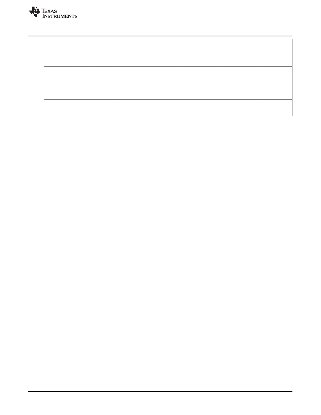
9 Bill of Materials
Designator Quant
C1 1 0.1uF CAP, CERM, 0.1 uF, 16 V, +/-
C1_S, C2_S,
C3_S, C4_S,
C5_S, C7
C2 1 1uF CAP, CERM, 1 uF, 16 V, +/-
C5, C6 2 0.022uF CAP, CERM, 0.022 uF, 25 V,
C8 1 100pF CAP, CERM, 100 pF, 10 V, +/-
C9, C10 2 22uF CAP, CERM, 22 uF, 50 V, +/-
D1, D2 2 200V Diode, Switching, 200 V, 0.2 A,
H1, H2, H3, H4 4 Machine Screw, Round, #4-40
H5, H6, H7, H8 4 Standoff, Hex, 0.5"L #4-40
J1, J2 2 Receptacle, 2.54mm, 12x1,
ity
6 0.1uF CAP, CERM, 0.1 uF, 50 V, +/-
Value Description PackageReference PartNumber Manufacturer
10%, X5R, 0402
10%, X7R, AEC-Q200 Grade 1,
0805
10%, X5R, 0805
+/- 10%, X7R, 0603
10%, X7R, 0603
20%, X5R, 6x5x5mm
SOT-23
x 1/4, Nylon, Philips panhead
Nylon
Gold, TH
0402 160R07X104KV4TJohanson
0805 GCM21BR71H1
0805 0805YD105KAT2AAVX
0603 C0603C223K3R
0603 0603ZC101KAT2AAVX
6x5x5mm CKG57NX5R1H
SOT-23 BAS21-7-F Diodes Inc.
Screw NY PMS 440
Standoff 1902C Keystone
Receptacle, 2.54mm,
12x1, TH
04KA37K
ACTU
226M500JH
0025 PH
801-47-012-10012000
Technology
MuRata
Kemet
TDK
B&F Fastener
Supply
Mill-Max
SLVUBD4A–January 2018–Revised December 2018
Submit Documentation Feedback
Copyright © 2018, Texas Instruments Incorporated
High Side Switch Motherboard Evaluation Module
11
Page 12

Bill of Materials
www.ti.com
J1_S, J2_S,
J3_S, J4_S,
J5_S, J6_S,
J7_S, J8_S,
J13_S, J14_S
J4, J5, J17, J18,
J19, J20, J21,
J22, J24
J6, J8, J9, J10,
J11, J12, J13
J9_S, J10_S,
J11_S, J12_S,
J15_S
J16 1 Receptacle, 2.54mm, 3x1, Tin,THReceptacle, 2.54mm,
J23, J26, J27,
J28
J25 1 BANANA JACK, SOLDER
R1 1 1.00k RES, 1.00 k, 1%, 0.1 W, AEC-
R1_S, R2_S,
R3_S, R4_S,
R5_S, R6_S,
R7_S, R8_S,
R9_S, R10_S
R2, R7, R11,
R12, R13, R14,
R15
R6 1 4.7k RES, 4.7 k, 5%, 0.1 W, AEC-
R16, R17 2 10k RES, 10 k, 5%, 0.1 W, AEC-
SH-J1, SH-J2,
SH-J3, SH-J4,
SH-J5, SH-J6,
SH-J7, SH-J8,
SH-J9, SH-J10
TP1, TP2, TP3,
TP4, TP5, TP6,
TP7, TP17,
TP18
TP8, TP10,
TP11, TP12
TP13, TP14,
TP15, TP16
U1 1 Single Output LDO, 150 mA,
C3 0 0.022uF CAP, CERM, 0.022 uF, 25 V,
C4 0 2.2uF CAP, CERM, 2.2 uF, 50 V, +/-
C11 0 47uF CAP, AL, 47 uF, 50 V, +/- 20%,
D3 0 39V Diode, TVS, Bi, 39 V, SMB SMB SM6T39CA STMicroelectroni
D4, D5, D6 0 30V Diode, TVS, Uni, 30 V, SMC SMC SMCJ30A Fairchild
10 Header, 100mil, 12x1, TH Header, 12x1, 100mil,TH800-10-012-10-
9 Header, 2.54mm, 2x1, Tin, TH Header, 2.54mm, 2x1,TH22284023 Molex
7 Header, 2.54mm, 3x1, Gold,THHeader, 2.54mm, 3x1,TH5-146280-3 TE Connectivity
5 Header, 100mil, 3x1, TH Header, 3x1, 100mil,TH800-10-003-10-
3x1, TH
4 BANANA JACK, SOLDER
LUG, RED, TH
LUG, BLACK, TH
Q200 Grade 0, 0603
10 10.0k RES, 10.0 k, 0.5%, 0.125 W,
0805
7 10k RES, 10 k, 5%, 0.1 W, 0603 0603 RC1608J103CS Samsung
Q200 Grade 0, 0603
Q200 Grade 0, 0603
10 1x2 Shunt, 100mil, Gold plated,
Black
9 Test Point, Multipurpose, Blue,THBlue Multipurpose
4 Test Point, Multipurpose, Red,THRed Multipurpose
4 Test Point, Multipurpose, Black,THBlack Multipurpose
Fixed 5 V Output, 2.5 to 24 V
Input, with Ultra-Low IQ, 5-pin
SOT-23 (DBV), -40 to 125
degC, Green (RoHS & no
Sb/Br)
+/- 10%, X7R, 0603
10%, X6S, 0805
0.68 ohm, AEC-Q200 Grade 2,
SMD
Red Insulated Banana
Jack
Black Insulated
Banana Jack
0603 CRCW06031K0
0805 RT0805DRE071
0603 CRCW06034K7
0603 CRCW060310K
Shunt SNT-100-BK-G Samtec
Testpoint
Testpoint
Testpoint
DBV0005A TLV70450DBVR Texas
0603 C0603C223K3R
0805 C2012X6S1H22
SMT Radial E EEE-FK1H470P Panasonic
001000
001000
801-47-003-10012000
SPC15363 Tenma
SPC15354 Tenma
0FKEA
0KL
0JNEA
0JNEA
5127 Keystone
5010 Keystone
5011 Keystone
ACTU
5K125AB
Mill-Max
Mill-Max
Mill-Max
Vishay-Dale
Yageo America
ElectroMechanics
Vishay-Dale
Vishay-Dale
Instruments
Kemet
TDK
cs
Semiconductor
12
High Side Switch Motherboard Evaluation Module
SLVUBD4A–January 2018–Revised December 2018
Submit Documentation Feedback
Copyright © 2018, Texas Instruments Incorporated
Page 13
www.ti.com
Bill of Materials
R3, R4 0 10k RES, 10 k, 5%, 0.1 W, 0603 0603 RC1608J103CS Samsung
R8, R9 0 0 RES, 0, 5%, 0.063 W, AEC-
U1_S 0 40-V, 8-mOhm Dual-Channel
U2, U2_S 0 40-V, 8-mOhm Dual-Channel
U3_S, U4_S,
U5_S
0 40-V, 16-mOhm Dual-Channel
Q200 Grade 0, 0402
Smart High-Side Switch,
PWP0024L (TSSOP-24)
Smart High-Side Switch,
PWP0024L (TSSOP-24)
Smart High-Side Switch,
TPS1HA08-Q1 (TSSOP-16)
0402 CRCW04020000
Z0ED
PWP0024L TPS2HB08DQP
WPRQ1
PWP0024L TPS2HB08BQP
WPRQ1
TPS1HA08-Q1 TPS2HB16BQP
WPRQ1
ElectroMechanics
Vishay-Dale
Texas
Instruments
Texas
Instruments
Texas
Instruments
SLVUBD4A–January 2018–Revised December 2018
Submit Documentation Feedback
Copyright © 2018, Texas Instruments Incorporated
High Side Switch Motherboard Evaluation Module
13
Page 14

STANDARD TERMS FOR EVALUATION MODULES
1. Delivery: TI delivers TI evaluation boards, kits, or modules, including any accompanying demonstration software, components, and/or
documentation which may be provided together or separately (collectively, an “EVM” or “EVMs”) to the User (“User”) in accordance
with the terms set forth herein. User's acceptance of the EVM is expressly subject to the following terms.
1.1 EVMs are intended solely for product or software developers for use in a research and development setting to facilitate feasibility
evaluation, experimentation, or scientific analysis of TI semiconductors products. EVMs have no direct function and are not
finished products. EVMs shall not be directly or indirectly assembled as a part or subassembly in any finished product. For
clarification, any software or software tools provided with the EVM (“Software”) shall not be subject to the terms and conditions
set forth herein but rather shall be subject to the applicable terms that accompany such Software
1.2 EVMs are not intended for consumer or household use. EVMs may not be sold, sublicensed, leased, rented, loaned, assigned,
or otherwise distributed for commercial purposes by Users, in whole or in part, or used in any finished product or production
system.
2 Limited Warranty and Related Remedies/Disclaimers:
2.1 These terms do not apply to Software. The warranty, if any, for Software is covered in the applicable Software License
Agreement.
2.2 TI warrants that the TI EVM will conform to TI's published specifications for ninety (90) days after the date TI delivers such EVM
to User. Notwithstanding the foregoing, TI shall not be liable for a nonconforming EVM if (a) the nonconformity was caused by
neglect, misuse or mistreatment by an entity other than TI, including improper installation or testing, or for any EVMs that have
been altered or modified in any way by an entity other than TI, (b) the nonconformity resulted from User's design, specifications
or instructions for such EVMs or improper system design, or (c) User has not paid on time. Testing and other quality control
techniques are used to the extent TI deems necessary. TI does not test all parameters of each EVM.
User's claims against TI under this Section 2 are void if User fails to notify TI of any apparent defects in the EVMs within ten (10)
business days after delivery, or of any hidden defects with ten (10) business days after the defect has been detected.
2.3 TI's sole liability shall be at its option to repair or replace EVMs that fail to conform to the warranty set forth above, or credit
User's account for such EVM. TI's liability under this warranty shall be limited to EVMs that are returned during the warranty
period to the address designated by TI and that are determined by TI not to conform to such warranty. If TI elects to repair or
replace such EVM, TI shall have a reasonable time to repair such EVM or provide replacements. Repaired EVMs shall be
warranted for the remainder of the original warranty period. Replaced EVMs shall be warranted for a new full ninety (90) day
warranty period.
3 Regulatory Notices:
3.1 United States
3.1.1 Notice applicable to EVMs not FCC-Approved:
FCC NOTICE: This kit is designed to allow product developers to evaluate electronic components, circuitry, or software
associated with the kit to determine whether to incorporate such items in a finished product and software developers to write
software applications for use with the end product. This kit is not a finished product and when assembled may not be resold or
otherwise marketed unless all required FCC equipment authorizations are first obtained. Operation is subject to the condition
that this product not cause harmful interference to licensed radio stations and that this product accept harmful interference.
Unless the assembled kit is designed to operate under part 15, part 18 or part 95 of this chapter, the operator of the kit must
operate under the authority of an FCC license holder or must secure an experimental authorization under part 5 of this chapter.
3.1.2 For EVMs annotated as FCC – FEDERAL COMMUNICATIONS COMMISSION Part 15 Compliant:
CAUTION
This device complies with part 15 of the FCC Rules. Operation is subject to the following two conditions: (1) This device may not
cause harmful interference, and (2) this device must accept any interference received, including interference that may cause
undesired operation.
Changes or modifications not expressly approved by the party responsible for compliance could void the user's authority to
operate the equipment.
FCC Interference Statement for Class A EVM devices
NOTE: This equipment has been tested and found to comply with the limits for a Class A digital device, pursuant to part 15 of
the FCC Rules. These limits are designed to provide reasonable protection against harmful interference when the equipment is
operated in a commercial environment. This equipment generates, uses, and can radiate radio frequency energy and, if not
installed and used in accordance with the instruction manual, may cause harmful interference to radio communications.
Operation of this equipment in a residential area is likely to cause harmful interference in which case the user will be required to
correct the interference at his own expense.
Page 15

FCC Interference Statement for Class B EVM devices
NOTE: This equipment has been tested and found to comply with the limits for a Class B digital device, pursuant to part 15 of
the FCC Rules. These limits are designed to provide reasonable protection against harmful interference in a residential
installation. This equipment generates, uses and can radiate radio frequency energy and, if not installed and used in accordance
with the instructions, may cause harmful interference to radio communications. However, there is no guarantee that interference
will not occur in a particular installation. If this equipment does cause harmful interference to radio or television reception, which
can be determined by turning the equipment off and on, the user is encouraged to try to correct the interference by one or more
of the following measures:
• Reorient or relocate the receiving antenna.
• Increase the separation between the equipment and receiver.
• Connect the equipment into an outlet on a circuit different from that to which the receiver is connected.
• Consult the dealer or an experienced radio/TV technician for help.
3.2 Canada
3.2.1 For EVMs issued with an Industry Canada Certificate of Conformance to RSS-210 or RSS-247
Concerning EVMs Including Radio Transmitters:
This device complies with Industry Canada license-exempt RSSs. Operation is subject to the following two conditions:
(1) this device may not cause interference, and (2) this device must accept any interference, including interference that may
cause undesired operation of the device.
Concernant les EVMs avec appareils radio:
Le présent appareil est conforme aux CNR d'Industrie Canada applicables aux appareils radio exempts de licence. L'exploitation
est autorisée aux deux conditions suivantes: (1) l'appareil ne doit pas produire de brouillage, et (2) l'utilisateur de l'appareil doit
accepter tout brouillage radioélectrique subi, même si le brouillage est susceptible d'en compromettre le fonctionnement.
Concerning EVMs Including Detachable Antennas:
Under Industry Canada regulations, this radio transmitter may only operate using an antenna of a type and maximum (or lesser)
gain approved for the transmitter by Industry Canada. To reduce potential radio interference to other users, the antenna type
and its gain should be so chosen that the equivalent isotropically radiated power (e.i.r.p.) is not more than that necessary for
successful communication. This radio transmitter has been approved by Industry Canada to operate with the antenna types
listed in the user guide with the maximum permissible gain and required antenna impedance for each antenna type indicated.
Antenna types not included in this list, having a gain greater than the maximum gain indicated for that type, are strictly prohibited
for use with this device.
Concernant les EVMs avec antennes détachables
Conformément à la réglementation d'Industrie Canada, le présent émetteur radio peut fonctionner avec une antenne d'un type et
d'un gain maximal (ou inférieur) approuvé pour l'émetteur par Industrie Canada. Dans le but de réduire les risques de brouillage
radioélectrique à l'intention des autres utilisateurs, il faut choisir le type d'antenne et son gain de sorte que la puissance isotrope
rayonnée équivalente (p.i.r.e.) ne dépasse pas l'intensité nécessaire à l'établissement d'une communication satisfaisante. Le
présent émetteur radio a été approuvé par Industrie Canada pour fonctionner avec les types d'antenne énumérés dans le
manuel d’usage et ayant un gain admissible maximal et l'impédance requise pour chaque type d'antenne. Les types d'antenne
non inclus dans cette liste, ou dont le gain est supérieur au gain maximal indiqué, sont strictement interdits pour l'exploitation de
l'émetteur
3.3 Japan
3.3.1 Notice for EVMs delivered in Japan: Please see http://www.tij.co.jp/lsds/ti_ja/general/eStore/notice_01.page 日本国内に
輸入される評価用キット、ボードについては、次のところをご覧ください。
http://www.tij.co.jp/lsds/ti_ja/general/eStore/notice_01.page
3.3.2 Notice for Users of EVMs Considered “Radio Frequency Products” in Japan: EVMs entering Japan may not be certified
by TI as conforming to Technical Regulations of Radio Law of Japan.
If User uses EVMs in Japan, not certified to Technical Regulations of Radio Law of Japan, User is required to follow the
instructions set forth by Radio Law of Japan, which includes, but is not limited to, the instructions below with respect to EVMs
(which for the avoidance of doubt are stated strictly for convenience and should be verified by User):
1. Use EVMs in a shielded room or any other test facility as defined in the notification #173 issued by Ministry of Internal
Affairs and Communications on March 28, 2006, based on Sub-section 1.1 of Article 6 of the Ministry’s Rule for
Enforcement of Radio Law of Japan,
2. Use EVMs only after User obtains the license of Test Radio Station as provided in Radio Law of Japan with respect to
EVMs, or
3. Use of EVMs only after User obtains the Technical Regulations Conformity Certification as provided in Radio Law of Japan
with respect to EVMs. Also, do not transfer EVMs, unless User gives the same notice above to the transferee. Please note
that if User does not follow the instructions above, User will be subject to penalties of Radio Law of Japan.
Page 16

【無線電波を送信する製品の開発キットをお使いになる際の注意事項】 開発キットの中には技術基準適合証明を受けて
いないものがあります。 技術適合証明を受けていないもののご使用に際しては、電波法遵守のため、以下のいずれかの
措置を取っていただく必要がありますのでご注意ください。
1. 電波法施行規則第6条第1項第1号に基づく平成18年3月28日総務省告示第173号で定められた電波暗室等の試験設備でご使用
いただく。
2. 実験局の免許を取得後ご使用いただく。
3. 技術基準適合証明を取得後ご使用いただく。
なお、本製品は、上記の「ご使用にあたっての注意」を譲渡先、移転先に通知しない限り、譲渡、移転できないものとします。
上記を遵守頂けない場合は、電波法の罰則が適用される可能性があることをご留意ください。 日本テキサス・イ
ンスツルメンツ株式会社
東京都新宿区西新宿6丁目24番1号
西新宿三井ビル
3.3.3 Notice for EVMs for Power Line Communication: Please see http://www.tij.co.jp/lsds/ti_ja/general/eStore/notice_02.page
電力線搬送波通信についての開発キットをお使いになる際の注意事項については、次のところをご覧ください。http:/
/www.tij.co.jp/lsds/ti_ja/general/eStore/notice_02.page
3.4 European Union
3.4.1 For EVMs subject to EU Directive 2014/30/EU (Electromagnetic Compatibility Directive):
This is a class A product intended for use in environments other than domestic environments that are connected to a
low-voltage power-supply network that supplies buildings used for domestic purposes. In a domestic environment this
product may cause radio interference in which case the user may be required to take adequate measures.
4 EVM Use Restrictions and Warnings:
4.1 EVMS ARE NOT FOR USE IN FUNCTIONAL SAFETY AND/OR SAFETY CRITICAL EVALUATIONS, INCLUDING BUT NOT
LIMITED TO EVALUATIONS OF LIFE SUPPORT APPLICATIONS.
4.2 User must read and apply the user guide and other available documentation provided by TI regarding the EVM prior to handling
or using the EVM, including without limitation any warning or restriction notices. The notices contain important safety information
related to, for example, temperatures and voltages.
4.3 Safety-Related Warnings and Restrictions:
4.3.1 User shall operate the EVM within TI’s recommended specifications and environmental considerations stated in the user
guide, other available documentation provided by TI, and any other applicable requirements and employ reasonable and
customary safeguards. Exceeding the specified performance ratings and specifications (including but not limited to input
and output voltage, current, power, and environmental ranges) for the EVM may cause personal injury or death, or
property damage. If there are questions concerning performance ratings and specifications, User should contact a TI
field representative prior to connecting interface electronics including input power and intended loads. Any loads applied
outside of the specified output range may also result in unintended and/or inaccurate operation and/or possible
permanent damage to the EVM and/or interface electronics. Please consult the EVM user guide prior to connecting any
load to the EVM output. If there is uncertainty as to the load specification, please contact a TI field representative.
During normal operation, even with the inputs and outputs kept within the specified allowable ranges, some circuit
components may have elevated case temperatures. These components include but are not limited to linear regulators,
switching transistors, pass transistors, current sense resistors, and heat sinks, which can be identified using the
information in the associated documentation. When working with the EVM, please be aware that the EVM may become
very warm.
4.3.2 EVMs are intended solely for use by technically qualified, professional electronics experts who are familiar with the
dangers and application risks associated with handling electrical mechanical components, systems, and subsystems.
User assumes all responsibility and liability for proper and safe handling and use of the EVM by User or its employees,
affiliates, contractors or designees. User assumes all responsibility and liability to ensure that any interfaces (electronic
and/or mechanical) between the EVM and any human body are designed with suitable isolation and means to safely
limit accessible leakage currents to minimize the risk of electrical shock hazard. User assumes all responsibility and
liability for any improper or unsafe handling or use of the EVM by User or its employees, affiliates, contractors or
designees.
4.4 User assumes all responsibility and liability to determine whether the EVM is subject to any applicable international, federal,
state, or local laws and regulations related to User’s handling and use of the EVM and, if applicable, User assumes all
responsibility and liability for compliance in all respects with such laws and regulations. User assumes all responsibility and
liability for proper disposal and recycling of the EVM consistent with all applicable international, federal, state, and local
requirements.
5. Accuracy of Information: To the extent TI provides information on the availability and function of EVMs, TI attempts to be as accurate
as possible. However, TI does not warrant the accuracy of EVM descriptions, EVM availability or other information on its websites as
accurate, complete, reliable, current, or error-free.
Page 17

6. Disclaimers:
6.1 EXCEPT AS SET FORTH ABOVE, EVMS AND ANY MATERIALS PROVIDED WITH THE EVM (INCLUDING, BUT NOT
LIMITED TO, REFERENCE DESIGNS AND THE DESIGN OF THE EVM ITSELF) ARE PROVIDED "AS IS" AND "WITH ALL
FAULTS." TI DISCLAIMS ALL OTHER WARRANTIES, EXPRESS OR IMPLIED, REGARDING SUCH ITEMS, INCLUDING BUT
NOT LIMITED TO ANY EPIDEMIC FAILURE WARRANTY OR IMPLIED WARRANTIES OF MERCHANTABILITY OR FITNESS
FOR A PARTICULAR PURPOSE OR NON-INFRINGEMENT OF ANY THIRD PARTY PATENTS, COPYRIGHTS, TRADE
SECRETS OR OTHER INTELLECTUAL PROPERTY RIGHTS.
6.2 EXCEPT FOR THE LIMITED RIGHT TO USE THE EVM SET FORTH HEREIN, NOTHING IN THESE TERMS SHALL BE
CONSTRUED AS GRANTING OR CONFERRING ANY RIGHTS BY LICENSE, PATENT, OR ANY OTHER INDUSTRIAL OR
INTELLECTUAL PROPERTY RIGHT OF TI, ITS SUPPLIERS/LICENSORS OR ANY OTHER THIRD PARTY, TO USE THE
EVM IN ANY FINISHED END-USER OR READY-TO-USE FINAL PRODUCT, OR FOR ANY INVENTION, DISCOVERY OR
IMPROVEMENT, REGARDLESS OF WHEN MADE, CONCEIVED OR ACQUIRED.
7. USER'S INDEMNITY OBLIGATIONS AND REPRESENTATIONS. USER WILL DEFEND, INDEMNIFY AND HOLD TI, ITS
LICENSORS AND THEIR REPRESENTATIVES HARMLESS FROM AND AGAINST ANY AND ALL CLAIMS, DAMAGES, LOSSES,
EXPENSES, COSTS AND LIABILITIES (COLLECTIVELY, "CLAIMS") ARISING OUT OF OR IN CONNECTION WITH ANY
HANDLING OR USE OF THE EVM THAT IS NOT IN ACCORDANCE WITH THESE TERMS. THIS OBLIGATION SHALL APPLY
WHETHER CLAIMS ARISE UNDER STATUTE, REGULATION, OR THE LAW OF TORT, CONTRACT OR ANY OTHER LEGAL
THEORY, AND EVEN IF THE EVM FAILS TO PERFORM AS DESCRIBED OR EXPECTED.
8. Limitations on Damages and Liability:
8.1 General Limitations. IN NO EVENT SHALL TI BE LIABLE FOR ANY SPECIAL, COLLATERAL, INDIRECT, PUNITIVE,
INCIDENTAL, CONSEQUENTIAL, OR EXEMPLARY DAMAGES IN CONNECTION WITH OR ARISING OUT OF THESE
TERMS OR THE USE OF THE EVMS , REGARDLESS OF WHETHER TI HAS BEEN ADVISED OF THE POSSIBILITY OF
SUCH DAMAGES. EXCLUDED DAMAGES INCLUDE, BUT ARE NOT LIMITED TO, COST OF REMOVAL OR
REINSTALLATION, ANCILLARY COSTS TO THE PROCUREMENT OF SUBSTITUTE GOODS OR SERVICES, RETESTING,
OUTSIDE COMPUTER TIME, LABOR COSTS, LOSS OF GOODWILL, LOSS OF PROFITS, LOSS OF SAVINGS, LOSS OF
USE, LOSS OF DATA, OR BUSINESS INTERRUPTION. NO CLAIM, SUIT OR ACTION SHALL BE BROUGHT AGAINST TI
MORE THAN TWELVE (12) MONTHS AFTER THE EVENT THAT GAVE RISE TO THE CAUSE OF ACTION HAS
OCCURRED.
8.2 Specific Limitations. IN NO EVENT SHALL TI'S AGGREGATE LIABILITY FROM ANY USE OF AN EVM PROVIDED
HEREUNDER, INCLUDING FROM ANY WARRANTY, INDEMITY OR OTHER OBLIGATION ARISING OUT OF OR IN
CONNECTION WITH THESE TERMS, , EXCEED THE TOTAL AMOUNT PAID TO TI BY USER FOR THE PARTICULAR
EVM(S) AT ISSUE DURING THE PRIOR TWELVE (12) MONTHS WITH RESPECT TO WHICH LOSSES OR DAMAGES ARE
CLAIMED. THE EXISTENCE OF MORE THAN ONE CLAIM SHALL NOT ENLARGE OR EXTEND THIS LIMIT.
9. Return Policy. Except as otherwise provided, TI does not offer any refunds, returns, or exchanges. Furthermore, no return of EVM(s)
will be accepted if the package has been opened and no return of the EVM(s) will be accepted if they are damaged or otherwise not in
a resalable condition. If User feels it has been incorrectly charged for the EVM(s) it ordered or that delivery violates the applicable
order, User should contact TI. All refunds will be made in full within thirty (30) working days from the return of the components(s),
excluding any postage or packaging costs.
10. Governing Law: These terms and conditions shall be governed by and interpreted in accordance with the laws of the State of Texas,
without reference to conflict-of-laws principles. User agrees that non-exclusive jurisdiction for any dispute arising out of or relating to
these terms and conditions lies within courts located in the State of Texas and consents to venue in Dallas County, Texas.
Notwithstanding the foregoing, any judgment may be enforced in any United States or foreign court, and TI may seek injunctive relief
in any United States or foreign court.
Mailing Address: Texas Instruments, Post Office Box 655303, Dallas, Texas 75265
Copyright © 2018, Texas Instruments Incorporated
Page 18

IMPORTANT NOTICE AND DISCLAIMER
TI PROVIDES TECHNICAL AND RELIABILITY DATA (INCLUDING DATASHEETS), DESIGN RESOURCES (INCLUDING REFERENCE
DESIGNS), APPLICATION OR OTHER DESIGN ADVICE, WEB TOOLS, SAFETY INFORMATION, AND OTHER RESOURCES “AS IS”
AND WITH ALL FAULTS, AND DISCLAIMS ALL WARRANTIES, EXPRESS AND IMPLIED, INCLUDING WITHOUT LIMITATION ANY
IMPLIED WARRANTIES OF MERCHANTABILITY, FITNESS FOR A PARTICULAR PURPOSE OR NON-INFRINGEMENT OF THIRD
PARTY INTELLECTUAL PROPERTY RIGHTS.
These resources are intended for skilled developers designing with TI products. You are solely responsible for (1) selecting the appropriate
TI products for your application, (2) designing, validating and testing your application, and (3) ensuring your application meets applicable
standards, and any other safety, security, or other requirements. These resources are subject to change without notice. TI grants you
permission to use these resources only for development of an application that uses the TI products described in the resource. Other
reproduction and display of these resources is prohibited. No license is granted to any other TI intellectual property right or to any third
party intellectual property right. TI disclaims responsibility for, and you will fully indemnify TI and its representatives against, any claims,
damages, costs, losses, and liabilities arising out of your use of these resources.
TI’s products are provided subject to TI’s Terms of Sale (www.ti.com/legal/termsofsale.html) or other applicable terms available either on
ti.com or provided in conjunction with such TI products. TI’s provision of these resources does not expand or otherwise alter TI’s applicable
warranties or warranty disclaimers for TI products.
Mailing Address: Texas Instruments, Post Office Box 655303, Dallas, Texas 75265
Copyright © 2018, Texas Instruments Incorporated
 Loading...