

Page 1
User's Guide
SNLU233–October 2017
LVDS83BTSSOPEVM User’s Guide
The SN75LVDS83B FlatLink™ transmitter contains the following functions within a single integrated
circuit:
• Four 7-bit, parallel-load, serial-out, shift registers
• A 7x clock synthesizer
• Five low-voltage differential signaling (LVDS) line drivers
These functions allow 28 bits of single-ended LVTTL data to be synchronously transmitted over five
balanced-pair conductors for receipt by a compatible receiver, such as the SN75LVDS82 and LCD panels
with integrated LVDS receivers.
This evaluation module (EVM) acts as a reference design that can be easily modified for any projected
application. Target applications include the following:
• LCD panel drivers
• Ultra-mobile PCs (UMPCs)
• Netbook PCs
• Digital picture frames
Schematics and layout information are included at the end of the manual.
SNLU233–October 2017
Submit Documentation Feedback
Copyright © 2017, Texas Instruments Incorporated
LVDS83BTSSOPEVM User’s Guide
1
Page 2

www.ti.com
Contents
1 Introduction ................................................................................................................... 3
2 LVDS83BTSSOPEVM Configuration...................................................................................... 3
2.1 LVDS83BTSSOPEVM Kit Contents.............................................................................. 3
2.2 Description of EVM Board ......................................................................................... 3
2.3 Power-Up Sequence ............................................................................................... 4
2.4 Signal Connectivity ................................................................................................. 5
3 PCB Construction .......................................................................................................... 10
3.1 LVDS83BTSSOPEVM Board Layout ........................................................................... 10
4 LVDS83BTSSOPEVM Bill of Materials.................................................................................. 17
5 LVDS83BTSSOPEVM Schematics ...................................................................................... 18
List of Figures
1 LVDS83BTSSOPEVM ...................................................................................................... 3
2 Clock Rising Edge (High) Jumper Setting................................................................................ 4
3 Clock Falling Edge (Low) Jumper Setting................................................................................ 4
4 Active Shutdown/Clear Jumper Setting................................................................................... 4
5 24-Bit Color Host to 24-Bit LCD Panel Application With 2 MSB Transfer Over Fourth Data Channel .......... 6
6 24-Bit Color Host to 24-Bit LCD Panel Application With 2 LBS Transfer Over Fourth Data Channel............ 7
7 18-Bit Color Host to 18-Bit LCD Panel Application...................................................................... 8
8 12-Bit Color Host to 18-Bit LCD Panel Application...................................................................... 9
9 24-Bit Color Host to 18-Bit LCD Panel Application .................................................................... 10
10 LVDS83BTSSOPEVM Top Layer........................................................................................ 11
11 LVDS83BTSSOPEVM Layer 2 – GND.................................................................................. 12
12 LVDS83BTSSOPEVM Layer 3 – DUT GND............................................................................ 13
13 LVDS83BTSSOPEVM Layer 4 – V
.................................................................................... 14
CC
14 LVDS83BTSSOPEVM Layer 5 – GND.................................................................................. 15
15 LVDS83BTSSOPEVM Bottom Layer .................................................................................... 16
16 LVDS83BTSSOPEVM Schematics (1/3)................................................................................ 18
17 LVDS83BTSSOPEVM Schematics (2/3)................................................................................ 19
18 LVDS83BTSSOPEVM Schematic (3/3) ................................................................................. 20
1 BOM.......................................................................................................................... 17
Trademarks
FlatLink is a trademark of Texas Instruments.
2
LVDS83BTSSOPEVM User’s Guide
List of Tables
Copyright © 2017, Texas Instruments Incorporated
SNLU233–October 2017
Submit Documentation Feedback
Page 3
CLKIN
CLKSEL
DUT_GND
SHTDN
DUT_GND
VCCIO DUT_GND SIGNAL_GND VCC
1p8V
2p5V
3p3V
3p3V
P1 P2 P3 P4
LVDS83BTSSOPEVM
INT061A
SIGNAL_GND
DUT_GND
Y2M
J6
Y0P
J9
Y1M
J8
J7
JMP6
U1
PIN 1
D19
D20
D21
D22
D24
D25
D26
D8
D9
D12
D13
D14
D15
D18
JMP4
JMP3
JMP2
JMP1
D0
D1
D2
D3
D4
D6
D7
D27
D5
D10
D11
D16
D17
D23
SIGNAL_GNDSIGNAL_GND
SIGNAL_GNDSIGNAL_GND
JMP7
JMP8
Y0M
J10
Y2P
J5
CLKINM
J2
Y3M
J4
Y3P
J3
CLKINP
J1
Y1P
C1
C3
C4
C5
C10
C9
C8
C7
C6
C11
C12
C13
C14
C15
C2
R2
R1
www.ti.com
1 Introduction
The SN75LVDS83B FlatLink transmitter is a single integrated circuit which contains four 7-bit, parallelload, serial-out, shift registers, a 7x clock synthesizer, and LVDS line drivers. This user’s guide describes
the construction and handling of the EVM for the SN75LVDS83B. The guide serves as an evaluation tool
for the SN75LVDS83B, as well as a reference design for the device.
Introduction
2 LVDS83BTSSOPEVM Configuration
2.1 LVDS83BTSSOPEVM Kit Contents
This EVM kit contains the following items:
• LVDS83BTSSOPEVM board
• LVDS83BTSSOPEVM User’s Guide
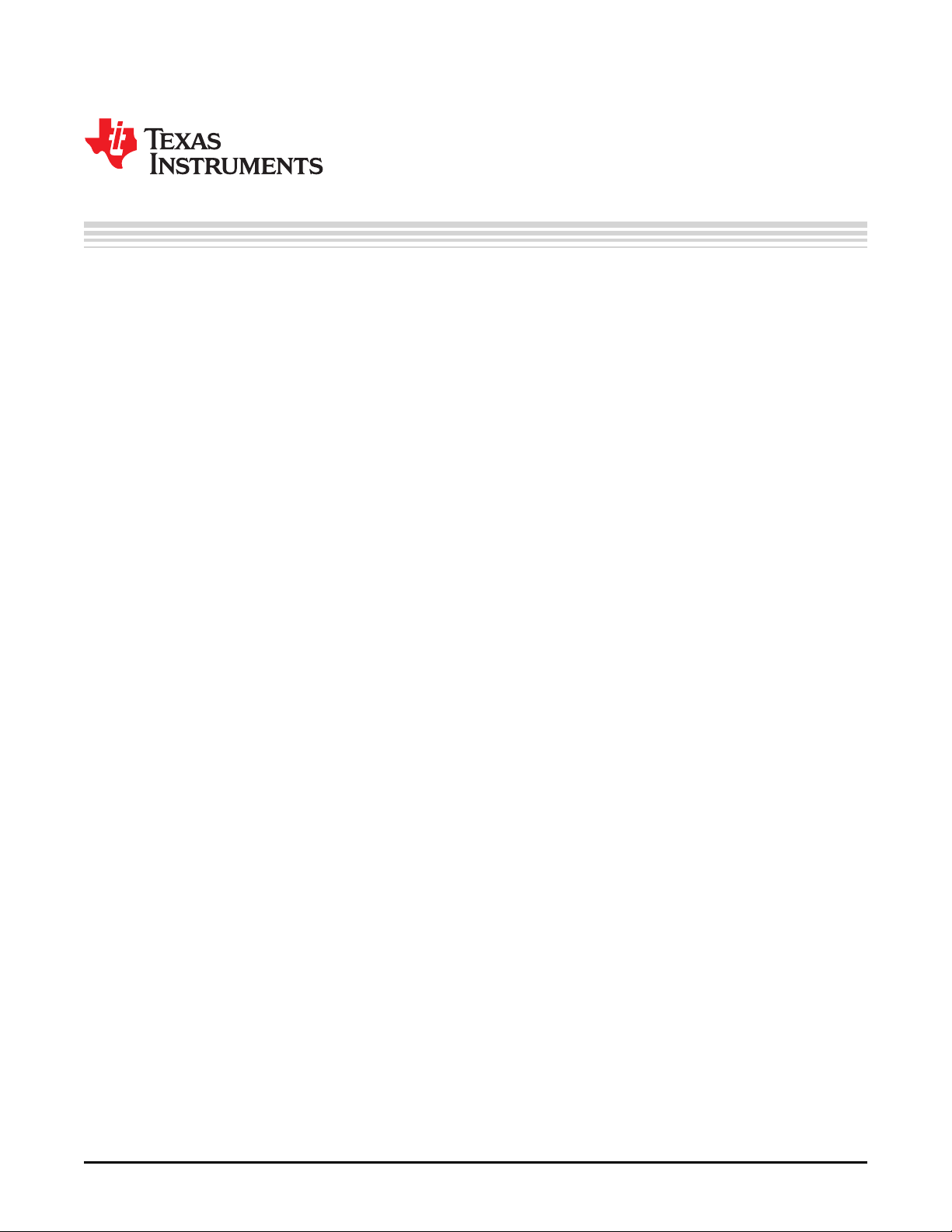
2.2 Description of EVM Board
The LVDS83BTSSOPEVM is designed to provide straightforward evaluation of the SN75LVDS83B device
using four 7-bit, parallel-load, serial-out, shift registers. Power to the board is provided through banana
jacks P4 for VCC and P1 for VCCIO. For correct board operation, power must be fixed at VCC = 3.3 V,
and the I/O power (VCCIO) may be adjusted at 1.8 V, 2.5 V, or 3.3 V.
The transmission of data bits D0 through D27 occurs as each bit is loaded into registers upon the edge of
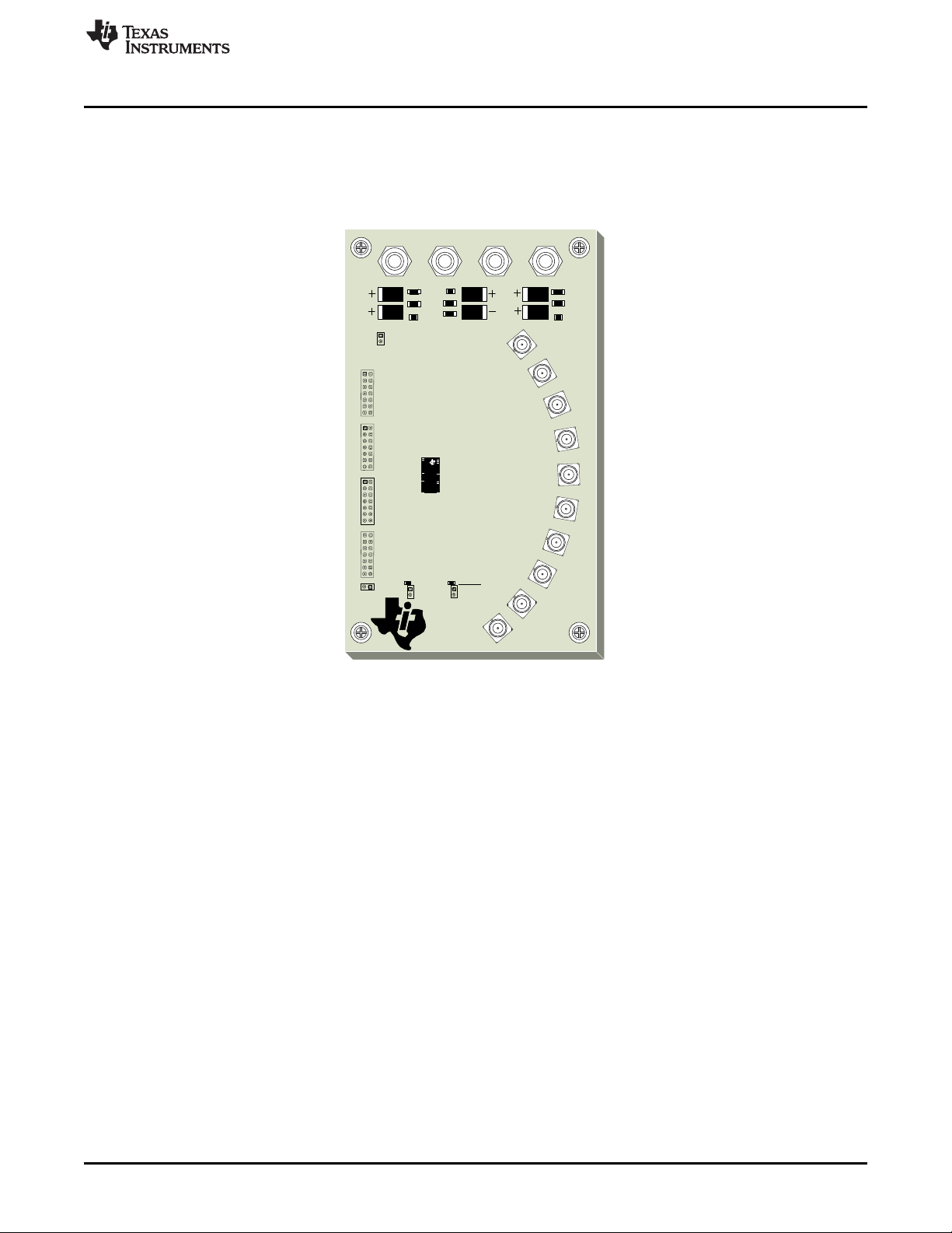
the CLKIN signal (JMP5), where the rising or falling edge of the clock may be selected using CLKSEL
(JMP7). To select a clock rising edge, input a high level to CLKSEL. Removing the strap on the jumper
allows the pull-up resistor to pull CLKSEL=high (see Figure 2). To input a low level to select a clock falling
edge, place the strap on the jumper to allow a path to GND (see Figure 3).
Additionally, use of SHTDN (JMP8) for possible Shutdown/Clear settings can be obtained with an activelow input, by placing the strap on the jumper to allow a path to GND, which inhibits the clock and shuts off
the LVDS output drivers for lower power consumption (see Figure 4). A low-level on this signal clears all
internal registers to a low-level. Remove the strap on JMP8 to enable the device for normal operation.
SNLU233–October 2017
Submit Documentation Feedback
Figure 1. LVDS83BTSSOPEVM
Copyright © 2017, Texas Instruments Incorporated
LVDS83BTSSOPEVM User’s Guide
3
Page 4
R2
SHTDN
DUT_GND
JMP8
Pull-up resistor
R1
CLKSEL
DUT_GND
JMP7
Pull-up resistor
R1
CLKSEL
DUT_GND
JMP7
Pull-up resistor
LVDS83BTSSOPEVM Configuration
Figure 2. Clock Rising Edge (High) Jumper Setting
Figure 3. Clock Falling Edge (Low) Jumper Setting
www.ti.com
2.3 Power-Up Sequence
The SN75LVDS83B does not require a specific power-up sequence; however, it is permitted to power up
the IOVCC while VCC, VCCPLL, and VCCLVDS remain powered down and connected to GND. The input
level of Shutdown/Clear during this time does not matter because only the input stage is powered up while
all other devices blocks are still powered down.
Additionally, it is also permitted to power up all 3.3 V power domains while IOVCC is still powered down to
GND. The device will not suffer damage. However, in this case, all the I/Os are detected as logic HIGH,
regardless of the input voltage level. Therefore connecting Shutdown/Clear to GND will still be interpreted
as logic HIGH, consequently turning the LVDS output stage on. The power consumption at this stage is
significantly higher that in standby mode, but lower than normal mode.
The user experience may be impacted by the way a system powers up and powers down an LCD screen.
The following sequences are suggested:
Power-up sequence (SN75LVDS83B SHTDN input initially LOW):
1. Ramp up the LCD power (0.5 ms to 10 ms) with the backlight turned off.
2. Wait an additional 0 to 200 ms to avoid display noise.
3. Enable the video source output – start sending black video data.
4
LVDS83BTSSOPEVM User’s Guide
Figure 4. Active Shutdown/Clear Jumper Setting
Copyright © 2017, Texas Instruments Incorporated
SNLU233–October 2017
Submit Documentation Feedback
Page 5

www.ti.com
4. Toggle SN75LVDS83B shutdown to SHTDN = VIH.
5. Send > 1 ms of black data to allow the SN75LVDS83B to be phase-locked and allow the display to
show black data first.
6. Start sending true imaging data.
7. Enable the backlight.
Power-down sequence (SN75LVDS83B SHTDN input initially HIGH):
1. Disable the LCD backlight and wait for the minimum time specified in the LCF data sheet for the
backlight to go low.
2. Switch the video source output data from active video to black data image (all visible pixels turn black)
on a drive > 2 frame times.
3. Set SN75LVDS83B SHTDN = GND and wait for 250 ns.
4. Disable the video output of the video source.
5. Remove power from the LCD panel for the lowest system power.
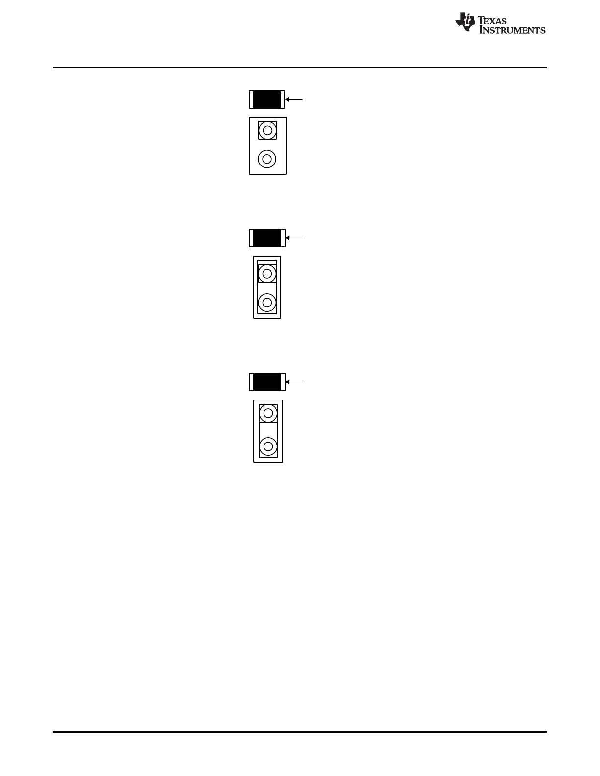
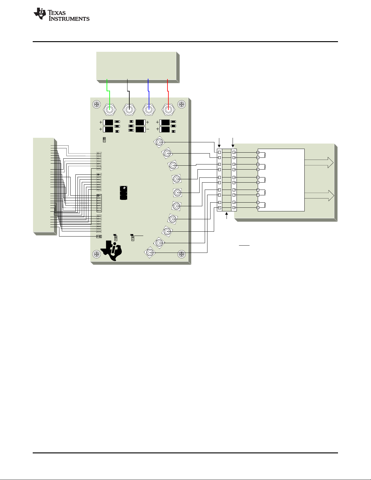
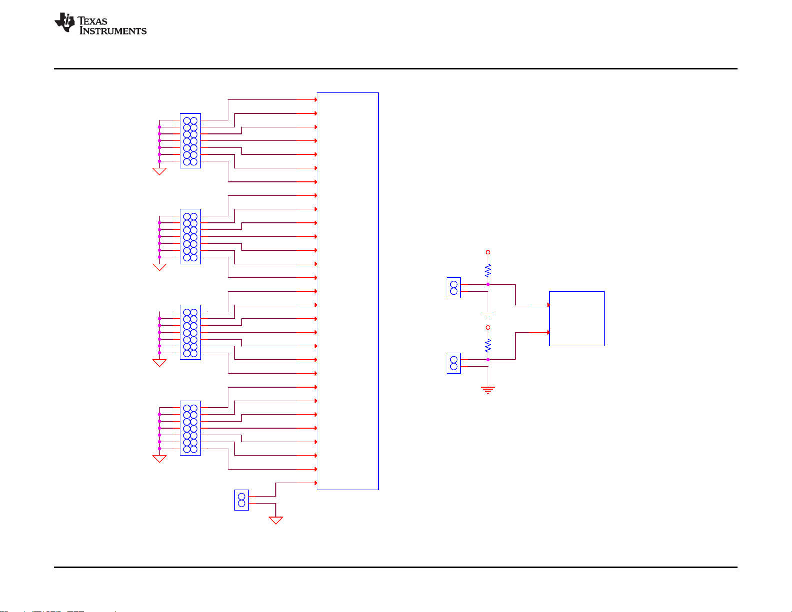
2.4 Signal Connectivity
While there is no formal, industrial standardization for the input interface of LVDS LCD panels, over the
years the industry has aligned a specific data bit order format. Figure 5 through Figure 9 show how each
signal must be connected from the graphic source through the SN75LVDS83B input/output and LVDS
LCD panel input.
The outputs are available at J1 to J10 for direct connection to oscilloscope inputs. Matched length cables
must be used when connecting the EVM to a scope to avoid inducing skew between the noninverting (+)
and inverting (-) outputs.
Power jacks P1 to P4 are used to provide power, ground, and signal ground reference for the EVM. The
power connections to the EVM determine the common-mode load to the device, because LVDS drivers
have limited common-mode driver capability. When connecting the EVM outputs directly to oscilloscope
inputs, setting the common-mode offset voltage of the oscilloscope is required, because it presents low
common-mode load impedance to the device.
In Figure 5 through Figure 9, the power supply is used to provide the required 3.3 V to the EVM.
Additionally, the signal ground input from the power supply is used to offset the EVM ground relative to the
DUT ground. Obtain optimum device setup by adjusting the signal ground voltage on the power supply
until its current is minimized. It is important to note that use of the dual supplies and offsetting the EVM
ground relative to the DUT ground are simply steps needed for the test and evaluation of devices. Actual
designs would include receivers 100-Ω termination resistor across each differential input while keeping a
high-impedance between each RX input signal and GND, which would not require the setup steps
previously outlined.
LVDS83BTSSOPEVM Configuration
SNLU233–October 2017
Submit Documentation Feedback
Copyright © 2017, Texas Instruments Incorporated
LVDS83BTSSOPEVM User’s Guide
5
Page 6
CLKIN
CLKSEL
DUT_GND
SHTDN
DUT_GND
Power Supply
GND
1p8V
2p5V
3p3V
1p2V 3p3V
VCCIO DUT_GND SIGNAL_GND VCC
1p8V
2p5V
3p3V
3p3V
P1 P2 P3 P4
LVDS83BTSSOPEVM
INT061A
SIGNAL_GND
DUT_GND
Y2M
J6
Y0P
J9
Y1M
J8
J7
JMP6
U1
PIN 1
D19
D20
D21
D22
D24
D25
D26
D8
D9
D12
D13
D14
D15
D18
JMP4
JMP3
JMP2
JMP1
D0
D1
D2
D3
D4
D6
D7
D27
D5
D10
D11
D16
D17
D23
SIGNAL_GNDSIGNAL_GND
SIGNAL_GNDSIGNAL_GND
JMP7
JMP8
Y0M
J10
Y2P
J5
CLKINM
J2
Y3M
J4
Y3P
J3
CLKINP
J1
Y1P
24bpp LCD Display
FPC Cable
LVDS
Timing
Controller
(8bpc, 24bpp)
Notes:
Current setup uses rising edge triggered clocking. If
rising edge triggered clocking is desired, place jumper
to create LOW level input at JMP7.
100
To Column Driver
Panel Connector
Main Board Connector
100
100
100
100
To Row Driver
24-bpc GPU
R0 (LSB)
R1
R2
R3
R4
R5
R6
R7 (MSB)
G0 (LSB)
G1
G2
G3
G4
G5
G6
G7 (MSB)
HSYNC
VSYNC
ENABLE
RSVD
CLK
B0 (LSB)
B1
B2
B3
B4
B5
B6
B7 (MSB)
C1
C3
C4
C5
C10
C9
C8
C7
C6
C11
C12
C13
C14
C15
C2
R2
R1
LVDS83BTSSOPEVM Configuration
www.ti.com
This configuration is most popular for 24-bit panels.
6
LVDS83BTSSOPEVM User’s Guide
Figure 5. 24-Bit Color Host to 24-Bit LCD Panel Application
With 2 MSB Transfer Over Fourth Data Channel
Copyright © 2017, Texas Instruments Incorporated
SNLU233–October 2017
Submit Documentation Feedback
Page 7
CLKSEL
DUT_GND
SHTDN
DUT_GND
Power Supply
GND
1p8V
2p5V
3p3V
1p2V 3p3V
VCCIO DUT_GND SIGNAL_GND VCC
1p8V
2p5V
3p3V
3p3V
P1 P2 P3 P4
LVDS83BTSSOPEVM
INT061A
SIGNAL_GND
DUT_GND
Y2M
J6
Y0P
J9
Y1M
J8
J7
JMP6
U1
PIN 1
JMP7
JMP8
Y0M
J10
Y2P
J5
CLKINM
J2
Y3M
J4
Y3P
J3
CLKINP
J1
Y1P
24bpp LCD Display
FPC Cable
LVDS
Timing
Controller
(8bpc, 24bpp)
Notes:
Current setup uses rising edge triggered clocking. If
rising edge triggered clocking is desired, place jumper
to create LOW level input at JMP7.
100
To Column Driver
Panel Connector
Main Board Connector
100
100
100
100
To Row Driver
24-bpc GPU
R0 (LSB)
R1
R2
R3
R4
R5
R6
R7 (MSB)
G0 (LSB)
G1
G2
G3
G4
G5
G6
G7 (MSB)
HSYNC
VSYNC
ENABLE
RSVD
CLK
B0 (LSB)
B1
B2
B3
B4
B5
B6
B7 (MSB)
CLKIN
D19
D20
D21
D22
D24
D25
D26
D8
D9
D12
D13
D14
D15
D18
JMP4
JMP3
JMP2
JMP1
D0
D1
D2
D3
D4
D6
D7
D27
D5
D10
D11
D16
D17
D23
SIGNAL_GNDSIGNAL_GND
SIGNAL_GNDSIGNAL_GND
C1
C3
C4
C5
C10
C9
C8
C7
C6
C11
C12
C13
C14
C15
C2
R2
R1
www.ti.com
LVDS83BTSSOPEVM Configuration
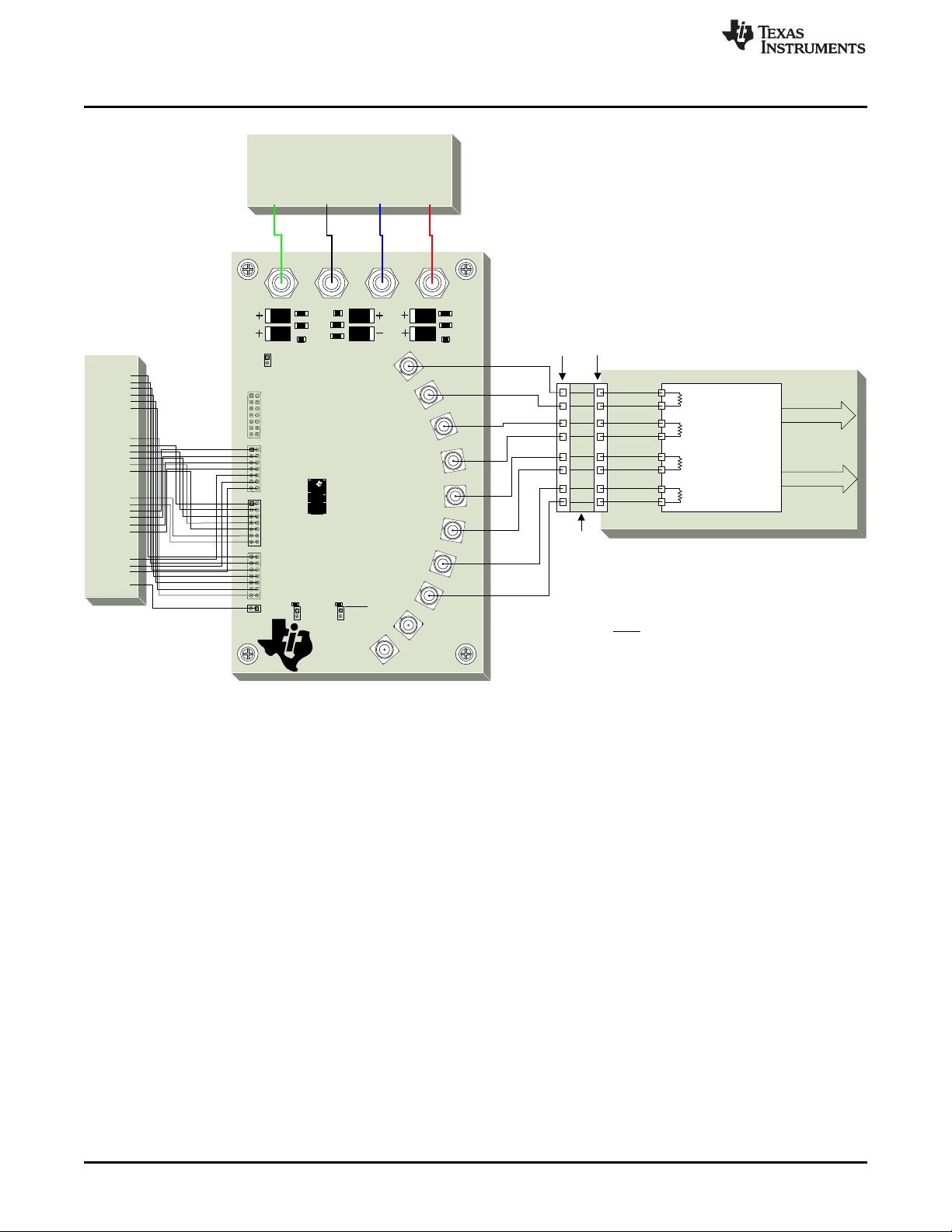
This configuration is fairly uncommon.
SNLU233–October 2017
Submit Documentation Feedback
Figure 6. 24-Bit Color Host to 24-Bit LCD Panel Application
With 2 LBS Transfer Over Fourth Data Channel
Copyright © 2017, Texas Instruments Incorporated
LVDS83BTSSOPEVM User’s Guide
7
Page 8
CLKSEL
DUT_GND
SHTDN
DUT_GND
Power Supply
GND
1p8V
2p5V
3p3V
1p2V 3p3V
VCCIO DUT_GND SIGNAL_GND VCC
1p8V
2p5V
3p3V
3p3V
P1 P2 P3 P4
LVDS83BTSSOPEVM
INT061A
SIGNAL_GND
DUT_GND
Y2M
J6
Y0P
J9
Y1M
J8
J7
U1
PIN 1
JMP7
JMP8
Y0M
J10
Y2P
J5
CLKINM
J2
Y3M
J4
Y3P
J3
CLKINP
J1
Y1P
LVDS
Timing
Controller
(8bpc, 18bpp)
Notes:
Current setup uses rising edge triggered clocking. If
rising edge triggered clocking is desired, place jumper
to create LOW level input at JMP7.
100
Panel Connector
Main Board Connector
100
100
100
18-bpc GPU
R0 (LSB)
R1
R2
R3
R4
R5 (MSB)
G0 (LSB)
G1
G2
G3
G4
G5 (MSB)
HSYNC
VSYNC
ENABLE
RSVD
CLK
B0 (LSB)
B1
B2
B3
B4
B5 (MSB)
24bpp LCD Display
FPC Cable
To Column Driver
To Row Driver
CLKIN
D19
D20
D21
D22
D24
D25
D26
D8
D9
D12
D13
D14
D15
D18
JMP4
JMP3
JMP2
JMP1
D0
D1
D2
D3
D4
D6
D7
D27
D5
D10
D11
D16
D17
D23
SIGNAL_GNDSIGNAL_GND
SIGNAL_GNDSIGNAL_GND
C1
C3
C4
C5
C10
C9
C8
C7
C6
C11
C12
C13
C14
C15
C2
R2
R1
LVDS83BTSSOPEVM Configuration
www.ti.com
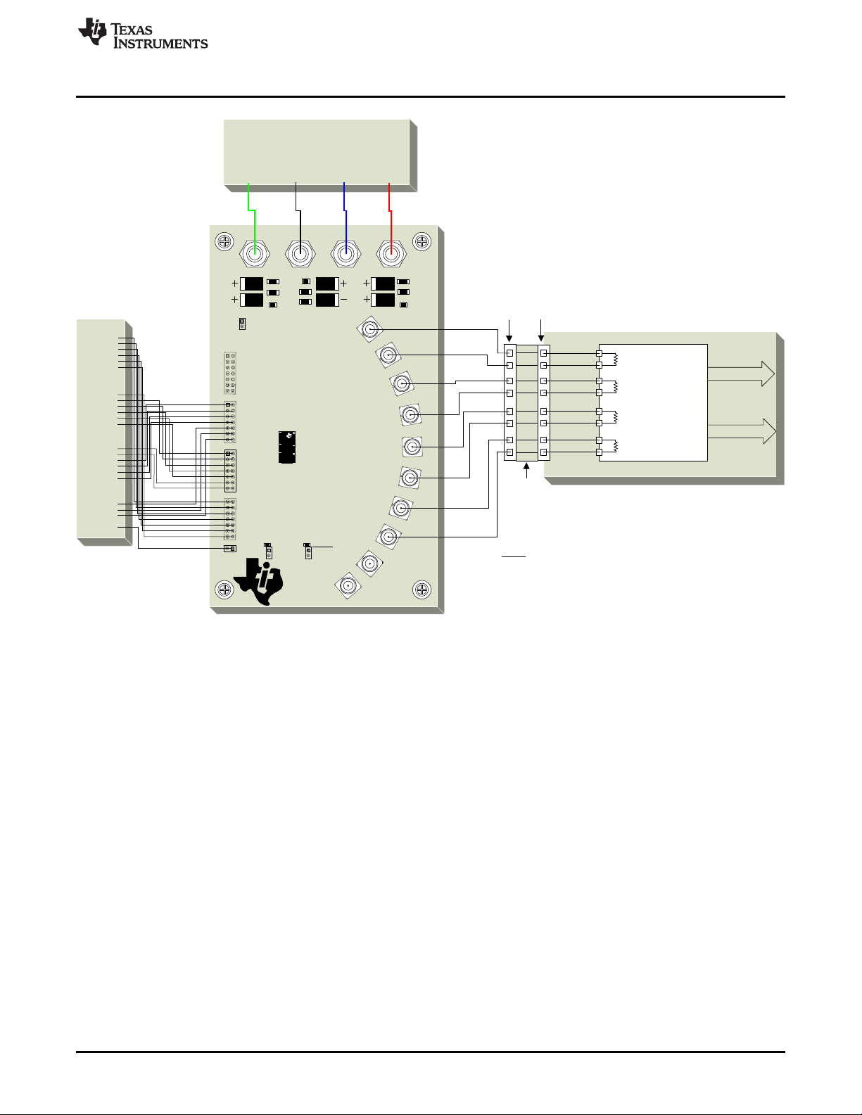
Figure 7. 18-Bit Color Host to 18-Bit LCD Panel Application
8
LVDS83BTSSOPEVM User’s Guide
Copyright © 2017, Texas Instruments Incorporated
SNLU233–October 2017
Submit Documentation Feedback
Page 9
CLKSEL
DUT_GND
SHTDN
DUT_GND
Power Supply
GND
1p8V
2p5V
3p3V
1p2V 3p3V
VCCIO DUT_GND SIGNAL_GND VCC
1p8V
2p5V
3p3V
3p3V
P1 P2 P3 P4
LVDS83BTSSOPEVM
INT061A
SIGNAL_GND
DUT_GND
Y2M
J6
Y0P
J9
Y1M
J8
J7
U1
PIN 1
JMP7
JMP8
Y0M
J10
Y2P
J5
CLKINM
J2
Y3M
J4
Y3P
J3
CLKINP
J1
Y1P
LVDS
Timing
Controller
(6bpc, 18bpp)
Notes:
Current setup uses rising edge triggered clocking. If rising edge triggered
clocking is desired, place jumper to create LOW level input at JMP7.
Leave output Y3 NC (No Connection).
*R3, G3, and B3 are MSB that may be connected to the 5th bit of each color
increased dynamics range of entire color space at the expense of nonlinear step sizes between each step. For linear steps with less dynamic
range, connect D1, D8, and D18 to GND.
*R32 G2, and B2 may be connected to the LSB of each color increased
dynamics range of entire color space at the expense of non-linear step
sizes between each step. For linear steps with less dynamic range,
connect D0, D7, and D15 to VCC.
100
Panel Connector
Main Board Connector
100
100
100
12-bpc GPU
R2 or Vcc*
R3 or GND*
R0 (LSB)
R1
R2
R3 (MSB)
G2 or Vcc*
G3 or GND*
G0 (LSB)
G1
G2
G3 (MSB)
HSYNC
VSYNC
ENABLE
RSVD
CLK
B2 or Vcc*
B3 or GND*
B0 (LSB)
B1
B2
B3 (MSB)
24bpp LCD Display
FPC Cable
To Column Driver
To Row Driver
CLKIN
D19
D20
D21
D22
D24
D25
D26
D8
D9
D12
D13
D14
D15
D18
JMP4
JMP3
JMP2
JMP1
D0
D1
D2
D3
D4
D6
D7
D27
D5
D10
D11
D16
D17
D23
SIGNAL_GNDSIGNAL_GND
SIGNAL_GNDSIGNAL_GND
C1
C3
C4
C5
C10
C9
C8
C7
C6
C11
C12
C13
C14
C15
C2
R2
R1
www.ti.com
LVDS83BTSSOPEVM Configuration
SNLU233–October 2017
Submit Documentation Feedback
Figure 8. 12-Bit Color Host to 18-Bit LCD Panel Application
Copyright © 2017, Texas Instruments Incorporated
LVDS83BTSSOPEVM User’s Guide
9
Page 10

24-bpc GPU
R0 (LSB)
R1
R2
R3
R4
R5
R6
R7 (MSB)
G0 (LSB)
G1
G2
G3
G4
G5
G6
G7 (MSB)
HSYNC
VSYNC
ENABLE
RSVD
CLK
B0 (LSB)
B1
B2
B3
B4
B5
B6
B7 (MSB)
CLKSEL
DUT_GND
SHTDN
DUT_GND
Power Supply
GND
1p8V
2p5V
3p3V
1p2V 3p3V
VCCIO DUT_GND SIGNAL_GND VCC
1p8V
2p5V
3p3V
3p3V
P1 P2 P3 P4
LVDS83BTSSOPEVM
INT061A
SIGNAL_GND
DUT_GND
Y2M
J6
Y0P
J9
Y1M
J8
J7
U1
PIN 1
JMP7
JMP8
Y0M
J10
Y2P
J5
CLKINM
J2
Y3M
J4
Y3P
J3
CLKINP
J1
Y1P
LVDS
Timing
Controller
(6bpc, 18bpp)
100
Panel Connector
Main Board Connector
100
100
100
24bpp LCD Display
FPC Cable
To Column Driver
To Row Driver
CLKIN
D19
D20
D21
D22
D24
D25
D26
D8
D9
D12
D13
D14
D15
D18
JMP4
JMP3
JMP2
JMP1
D0
D1
D2
D3
D4
D6
D7
D27
D5
D10
D11
D16
D17
D23
SIGNAL_GNDSIGNAL_GND
SIGNAL_GNDSIGNAL_GND
Notes:
Current setup uses rising edge triggered clocking. If rising edge triggered
clocking is desired, place jumper to create LOW level input at JMP7.
Leave output Y3 NC (No Connection).
R0, R1, G0, G1, B0 and B1 are for improved image quality purposes. The
GPU should dither 24-bit output pixel down to 18-bit per pixel.
C1
C3
C4
C5
C10
C9
C8
C7
C6
C11
C12
C13
C14
C15
C2
R2
R1
PCB Construction
www.ti.com
Figure 9. 24-Bit Color Host to 18-Bit LCD Panel Application
3 PCB Construction
This section discusses the construction of the LVDS83BTSSOPEVM boards. The section includes the
board layers to show how the board was built.
3.1 LVDS83BTSSOPEVM Board Layout
This EVM was designed to show the implementation of the SN75LVDS83B device on a 6-layer board.
The pin assignments of the input ports of the SN75LVDS83B device are optimized for the PCB mount of
10
the GPU connector. This allows easy routing of the traces and a minimal number of vias to preserve good
signal integrity. Every effort was made to keep the routing as clean as possible to the GPU connectors.
The board was designed to maintain 50 Ω to GND single-ended impedance for each individual trace. This
design uses FR4 – TurboClad 370 material with the board stack up shown in Figure 18, and requires the
traces to be 9.25 mil wide and 5 mils above the GND reference plane. A minimum spacing of 3 times the
trace width was maintained to all other components to prevent unwanted coupling.
A differential routing scheme that creates 100-Ω impedance between the differential traces could have
also been implemented equally as well with this device.
LVDS83BTSSOPEVM User’s Guide
Copyright © 2017, Texas Instruments Incorporated
SNLU233–October 2017
Submit Documentation Feedback
Page 11
www.ti.com
PCB Construction
SNLU233–October 2017
Submit Documentation Feedback
Figure 10. LVDS83BTSSOPEVM Top Layer
Copyright © 2017, Texas Instruments Incorporated
LVDS83BTSSOPEVM User’s Guide
11
Page 12

PCB Construction
www.ti.com
12
Figure 11. LVDS83BTSSOPEVM Layer 2 – GND
LVDS83BTSSOPEVM User’s Guide
Copyright © 2017, Texas Instruments Incorporated
SNLU233–October 2017
Submit Documentation Feedback
Page 13

www.ti.com
PCB Construction
SNLU233–October 2017
Submit Documentation Feedback
Figure 12. LVDS83BTSSOPEVM Layer 3 – DUT GND
LVDS83BTSSOPEVM User’s Guide
Copyright © 2017, Texas Instruments Incorporated
13
Page 14

PCB Construction
www.ti.com
14
Figure 13. LVDS83BTSSOPEVM Layer 4 – V
LVDS83BTSSOPEVM User’s Guide
Copyright © 2017, Texas Instruments Incorporated
CC
SNLU233–October 2017
Submit Documentation Feedback
Page 15
www.ti.com
PCB Construction
SNLU233–October 2017
Submit Documentation Feedback
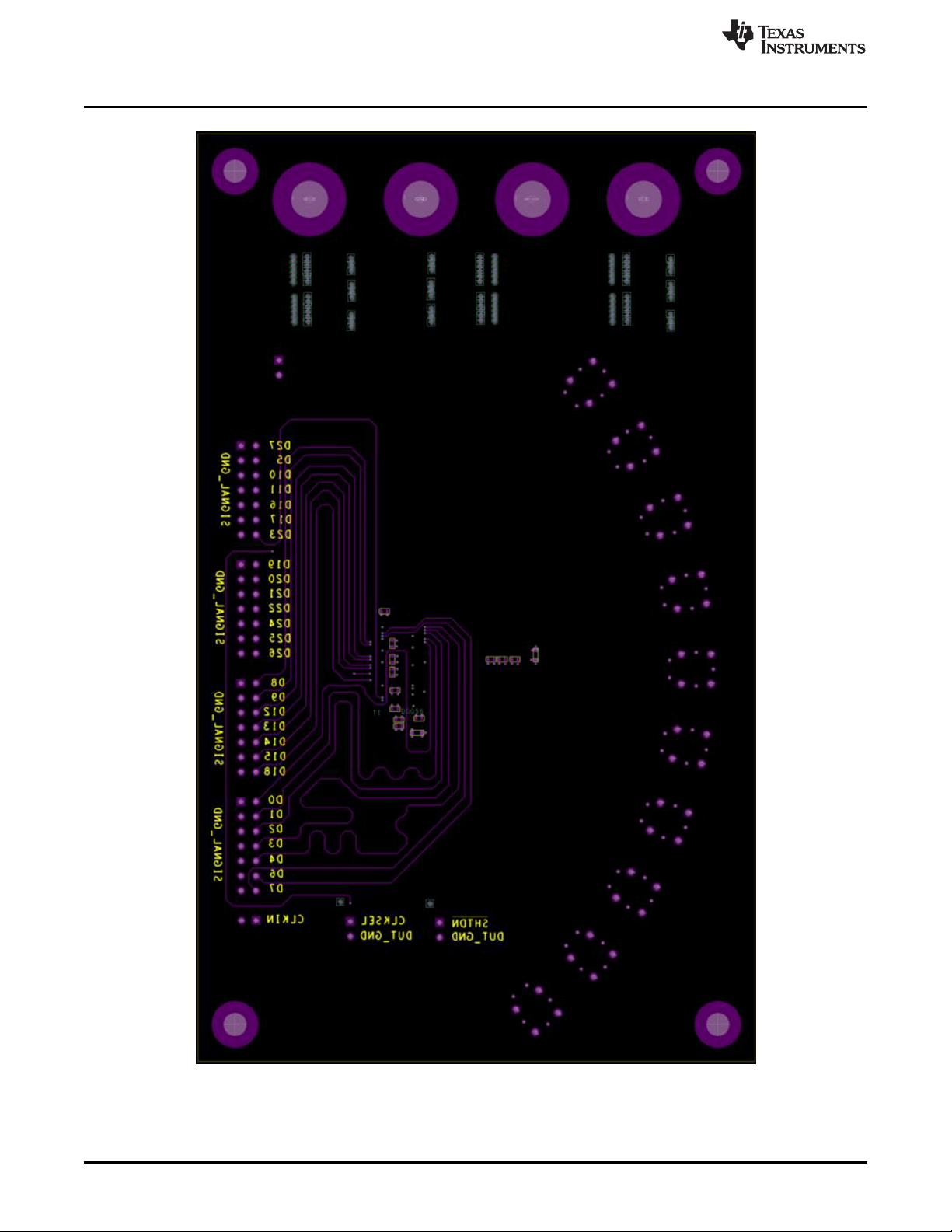
Figure 14. LVDS83BTSSOPEVM Layer 5 – GND
LVDS83BTSSOPEVM User’s Guide
Copyright © 2017, Texas Instruments Incorporated
15
Page 16
PCB Construction
www.ti.com
16
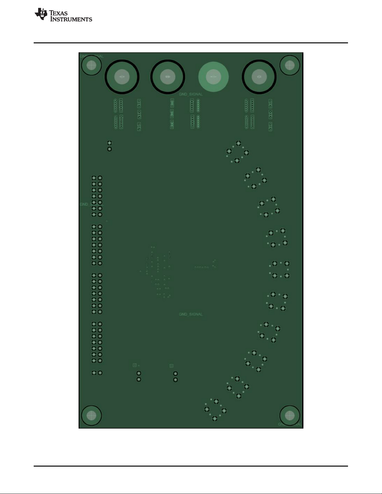
Figure 15. LVDS83BTSSOPEVM Bottom Layer
LVDS83BTSSOPEVM User’s Guide
Copyright © 2017, Texas Instruments Incorporated
SNLU233–October 2017
Submit Documentation Feedback
Page 17
www.ti.com
4 LVDS83BTSSOPEVM Bill of Materials
Table 1 lists the LVDS83BTSSOPEVM BOM.
Table 1. BOM
Item QTY Value Part Manufacturer Manufacture Part Number PCB Footprint Description
1 4 10000 pF
2 4 0.1 µF
3 4 1.0 µF
4 3 10000 pF C5, C10, C15 Würth Electronics 885012207011 CC0805
5 3 0.1 µF C4, C9, C14 Würth Electronics 885012208009 CC1206
6 3 1.0 µF C3, C8, C13 KEMET C1206C105K4RACTU CC1206
7 3 10 µF C2, C7, C12 KEMET C0805C106K8PACTU CC7343
8 3
9 2 0.0 Ω R3, R4 Panasonic - Ecg ERJ-3GEY0R00V R0603
10 2 4.75 KΩ R2, R1 Yageo RC0603FR-074K75L R0603
11 1
12 4 2 × 7
13 4 1 × 2
14 4
15 10 Jack
16 4
17 4
68 µF LESR
SN75LVDS
83B
Banana
Jack Metal
Round
Spacer
4 - 40 /
0.25
C22, C25, C19,
C16
C21, C24, C27,
C17
C20, C23, C26,
C18
C1, C6, C11 TDK C3216X5R0J686M160AB CC7343
U1 Texas Instruments SN75LVDS83B 56-TSSOP IC FlatLink XMITTER 56TSSOP
JMP1, JMP2,
JMP3, JMP4
JMP5, JMP7,
JMP8, JMP6
P1, P2, P3, P4
J10, J9, J8, J7,
J6, J5, J4, J3,
J2, J1
Standoffs Keystone Electronics 885 – Round spacer #6 NYLON 3/8"
Screws B&F Fastener Supply PMSSS 440 0025 PH Building Fasteners Machine screw pan Phillips 4 – 40
Samsung CL05B103KP5NNNC CC0402
Murata GRM155R61A104KA01D CC0402
Murata GRM155R61A105KE15D CC0402
Harwin M22-2520705 0.1 × 0.1"
Harwin M20-9990546 0.1 × 0.1"
Cinch Connectivity
Solutions Johnson
Power Co
Rosenberger 32K141-40ML5
108-0740-001 BJACK Connector, Jack Banana UNINS Panel MOU
32K141-40MFR4WVIA_2LAYER
10000 pF, ±10%, 10 V, ceramic capacitor X7R,
0402 (1005 metric)
0.1 µF, ±10%, 10 V, ceramic capacitor X5R, 0402
(1005 metric)
1 µF, ±10% 10 V, ceramic capacitor X5R, 0402
(1005 metric)
10000 pF, ±10%, 10 V, ceramic capacitor X7R,
0805 (2012 metric)
0.1 µF, ±10%, 10 V, ceramic capacitor X7R, 1206
(3216 metric)
1 µF, ±10%, 16 V, ceramic capacitor X7R, 1206
(3216 metric)
10 µF, ±10%, 10 V, ceramic capacitor X5R, 0805
(2012 metric)
68 µF, ±20%, 6.3 V, ceramic capacitor X5R, 1206
(3216 metric)
0.0-Ω jumper, 0.1 W, 1/10W, chip resistor 0603
(1608 metric), automotive AEC-Q200 thick film
4.75-kΩ, ±1%, 0.1 W, 1/10W, chip resistor, 0603
(1608 metric) moisture resistant thick film
14-position header, cuttable connector 0.079"
(2.00 mm) through hole gold
5-position header, cuttable connector 0.100" (2.54
mm) through hole tin
RF connectors / coaxial connectors SMA straight
jack PCB
LVDS83BTSSOPEVM Bill of Materials
SNLU233–October 2017
Submit Documentation Feedback
Copyright © 2017, Texas Instruments Incorporated
LVDS83BTSSOPEVM User’s Guide
17
Page 18
VCCIO
VCC
VCCIO
VCC
VCC
VCC
C4
.1uF
C10
.01uF
C22
.01uF
C14
.1uF
C15
.01uF
R3
0
P3
Banana-Jack
1
C6
68uF
U1D
SN75LVDS83B
Vcc
9
Vccio1
1
Vccio2
26
LVDSVcc
44
PLLVcc
34
C20
1uF
C3
1uF
C23
1uF
C12
10uF
C9
.1uF
C7
10uF
C24
.1uF
C25
.01uF
C11
68uF
C8
1uF
C21
.1uF
C18
1uF
C17
.1uF
JMP6
1
2
C13
1uF
C16
.01uF
U1C
SN75LVDS83B
GND1
5
GND2
13
GND3
21
GND4
29
GND5
53
PLLGND2
35
PLLGND1
33
LVDSGND3
49
LVDSGND2
43
LVDSGND1
36
P1
Banana-Jack
1
C26
1uF
P4
Banana jack
1
P2
Banana-Jack
1
C27
.1uF
C2
10uF
C5
.01uF
C1
68uF
C19
.01uF
R4
0
Copyright © 2017, Texas Instruments Incorporated
VCC and Bulk Bypass Capacitors
Signal Ground and Bulk Bypass Capacitor
Device Ground
VCCIO and Bulk Bypass Capacitors
Short to JMP9 to short
VCC = 3.3 V
GND_SIGNAL to GND_POWER
LVDS83BTSSOPEVM Schematics
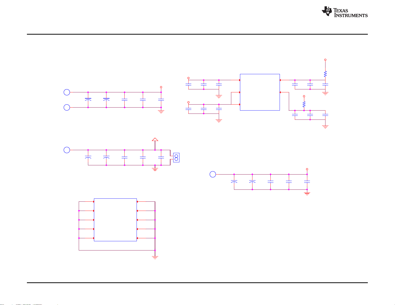
5 LVDS83BTSSOPEVM Schematics
Figure 16, Figure 17, and Figure 18 show the LVDS83BTSSOPEV schematics.
www.ti.com
18
LVDS83BTSSOPEVM User’s Guide
Figure 16. LVDS83BTSSOPEVM Schematics (1/3)
SNLU233–October 2017
Submit Documentation Feedback
Copyright © 2017, Texas Instruments Incorporated
Page 19
VCC
VCC
JMP4
Header 7x2
1
3
5
7
9
2
4
6
8
10
11 12
13 14
JMP2
Header 7x2
1
3
5
7
9
2
4
6
8
10
11 12
13 14
JMP7
1
2
JMP3
Header 7x2
1
3
5
7
9
2
4
6
8
10
11 12
13 14
U1E
SN75LVDS83B
CLKSEL
17
/SHTDN
32
R1
4.7k
R2
4.7k
JMP5
1
2
JMP8
1
2
JMP1
Header 7x2
1
3
5
7
9
2
4
6
8
10
11 12
13 14
U1B
SN75LVDS83B
D8
6
D9
7
D0
51
D1
52
D2
54
D3
55
D4
56
D6
3
D7
4
D12
11
D13
12
D14
14
D15
15
D18
19
D19
20
D20
22
D21
23
D22
24
D24
27
D25
28
D26
30
D27
50
D5
2
D10
8
D11
10
D16
16
D17
18
D23
25
CLKIN
31
Copyright © 2017, Texas Instruments Incorporated
VCC = 3.3 V
Clock Edge Select
Jumper high for rising edge
Jumper low for falling edge
Jumper high to enable device
Jumper low to disable device
www.ti.com
LVDS83BTSSOPEVM Schematics
SNLU233–October 2017
Submit Documentation Feedback
Figure 17. LVDS83BTSSOPEVM Schematics (2/3)
Copyright © 2017, Texas Instruments Incorporated
LVDS83BTSSOPEVM User’s Guide
19
Page 20
Channel 0 to 3
SMA SURFACE
J5
sma_surface
SMA SURFACE
J10
sma_surface
SMA SURFACE
J9
sma_surface
SMA SURFACE
J2
sma_surface
SMA SURFACE
J3
sma_surface
SMA SURFACE
J1
sma_surface
SMA SURFACE
J4
sma_surface
SMA SURFACE
J7
sma_surface
SMA SURFACE
J8
sma_surface
SMA SURFACE
J6
sma_surface
U1A
SN75LVDS83B
Y0M
48
Y0P
47
Y2P
41
42
Y2M
Y1P
45
Y3M
38
Y3P
37
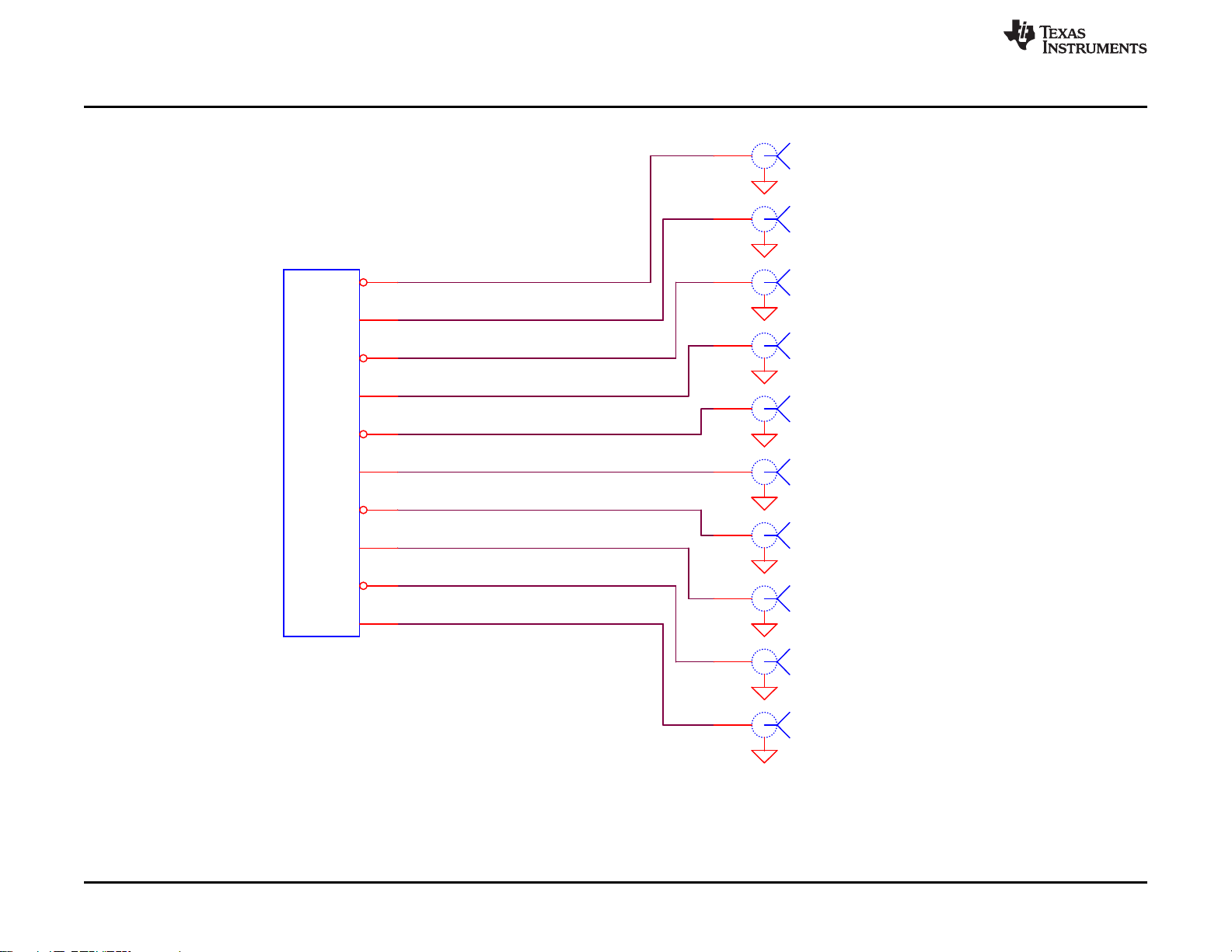
CLKOUTM
40
CLKOUTP
39
Y1M
46
Copyright © 2017, Texas Instruments Incorporated
LVDS83BTSSOPEVM Schematics
www.ti.com
20
LVDS83BTSSOPEVM User’s Guide
Figure 18. LVDS83BTSSOPEVM Schematic (3/3)
Copyright © 2017, Texas Instruments Incorporated
SNLU233–October 2017
Submit Documentation Feedback
Page 21

STANDARD TERMS FOR EVALUATION MODULES
1. Delivery: TI delivers TI evaluation boards, kits, or modules, including any accompanying demonstration software, components, and/or
documentation which may be provided together or separately (collectively, an “EVM” or “EVMs”) to the User (“User”) in accordance
with the terms set forth herein. User's acceptance of the EVM is expressly subject to the following terms.
1.1 EVMs are intended solely for product or software developers for use in a research and development setting to facilitate feasibility
evaluation, experimentation, or scientific analysis of TI semiconductors products. EVMs have no direct function and are not
finished products. EVMs shall not be directly or indirectly assembled as a part or subassembly in any finished product. For
clarification, any software or software tools provided with the EVM (“Software”) shall not be subject to the terms and conditions
set forth herein but rather shall be subject to the applicable terms that accompany such Software
1.2 EVMs are not intended for consumer or household use. EVMs may not be sold, sublicensed, leased, rented, loaned, assigned,
or otherwise distributed for commercial purposes by Users, in whole or in part, or used in any finished product or production
system.
2 Limited Warranty and Related Remedies/Disclaimers:
2.1 These terms do not apply to Software. The warranty, if any, for Software is covered in the applicable Software License
Agreement.
2.2 TI warrants that the TI EVM will conform to TI's published specifications for ninety (90) days after the date TI delivers such EVM
to User. Notwithstanding the foregoing, TI shall not be liable for a nonconforming EVM if (a) the nonconformity was caused by
neglect, misuse or mistreatment by an entity other than TI, including improper installation or testing, or for any EVMs that have
been altered or modified in any way by an entity other than TI, (b) the nonconformity resulted from User's design, specifications
or instructions for such EVMs or improper system design, or (c) User has not paid on time. Testing and other quality control
techniques are used to the extent TI deems necessary. TI does not test all parameters of each EVM.
User's claims against TI under this Section 2 are void if User fails to notify TI of any apparent defects in the EVMs within ten (10)
business days after delivery, or of any hidden defects with ten (10) business days after the defect has been detected.
2.3 TI's sole liability shall be at its option to repair or replace EVMs that fail to conform to the warranty set forth above, or credit
User's account for such EVM. TI's liability under this warranty shall be limited to EVMs that are returned during the warranty
period to the address designated by TI and that are determined by TI not to conform to such warranty. If TI elects to repair or
replace such EVM, TI shall have a reasonable time to repair such EVM or provide replacements. Repaired EVMs shall be
warranted for the remainder of the original warranty period. Replaced EVMs shall be warranted for a new full ninety (90) day
warranty period.
3 Regulatory Notices:
3.1 United States
3.1.1 Notice applicable to EVMs not FCC-Approved:
FCC NOTICE: This kit is designed to allow product developers to evaluate electronic components, circuitry, or software
associated with the kit to determine whether to incorporate such items in a finished product and software developers to write
software applications for use with the end product. This kit is not a finished product and when assembled may not be resold or
otherwise marketed unless all required FCC equipment authorizations are first obtained. Operation is subject to the condition
that this product not cause harmful interference to licensed radio stations and that this product accept harmful interference.
Unless the assembled kit is designed to operate under part 15, part 18 or part 95 of this chapter, the operator of the kit must
operate under the authority of an FCC license holder or must secure an experimental authorization under part 5 of this chapter.
3.1.2 For EVMs annotated as FCC – FEDERAL COMMUNICATIONS COMMISSION Part 15 Compliant:
CAUTION
This device complies with part 15 of the FCC Rules. Operation is subject to the following two conditions: (1) This device may not
cause harmful interference, and (2) this device must accept any interference received, including interference that may cause
undesired operation.
Changes or modifications not expressly approved by the party responsible for compliance could void the user's authority to
operate the equipment.
FCC Interference Statement for Class A EVM devices
NOTE: This equipment has been tested and found to comply with the limits for a Class A digital device, pursuant to part 15 of
the FCC Rules. These limits are designed to provide reasonable protection against harmful interference when the equipment is
operated in a commercial environment. This equipment generates, uses, and can radiate radio frequency energy and, if not
installed and used in accordance with the instruction manual, may cause harmful interference to radio communications.
Operation of this equipment in a residential area is likely to cause harmful interference in which case the user will be required to
correct the interference at his own expense.
Page 22

FCC Interference Statement for Class B EVM devices
NOTE: This equipment has been tested and found to comply with the limits for a Class B digital device, pursuant to part 15 of
the FCC Rules. These limits are designed to provide reasonable protection against harmful interference in a residential
installation. This equipment generates, uses and can radiate radio frequency energy and, if not installed and used in accordance
with the instructions, may cause harmful interference to radio communications. However, there is no guarantee that interference
will not occur in a particular installation. If this equipment does cause harmful interference to radio or television reception, which
can be determined by turning the equipment off and on, the user is encouraged to try to correct the interference by one or more
of the following measures:
• Reorient or relocate the receiving antenna.
• Increase the separation between the equipment and receiver.
• Connect the equipment into an outlet on a circuit different from that to which the receiver is connected.
• Consult the dealer or an experienced radio/TV technician for help.
3.2 Canada
3.2.1 For EVMs issued with an Industry Canada Certificate of Conformance to RSS-210 or RSS-247
Concerning EVMs Including Radio Transmitters:
This device complies with Industry Canada license-exempt RSSs. Operation is subject to the following two conditions:
(1) this device may not cause interference, and (2) this device must accept any interference, including interference that may
cause undesired operation of the device.
Concernant les EVMs avec appareils radio:
Le présent appareil est conforme aux CNR d'Industrie Canada applicables aux appareils radio exempts de licence. L'exploitation
est autorisée aux deux conditions suivantes: (1) l'appareil ne doit pas produire de brouillage, et (2) l'utilisateur de l'appareil doit
accepter tout brouillage radioélectrique subi, même si le brouillage est susceptible d'en compromettre le fonctionnement.
Concerning EVMs Including Detachable Antennas:
Under Industry Canada regulations, this radio transmitter may only operate using an antenna of a type and maximum (or lesser)
gain approved for the transmitter by Industry Canada. To reduce potential radio interference to other users, the antenna type
and its gain should be so chosen that the equivalent isotropically radiated power (e.i.r.p.) is not more than that necessary for
successful communication. This radio transmitter has been approved by Industry Canada to operate with the antenna types
listed in the user guide with the maximum permissible gain and required antenna impedance for each antenna type indicated.
Antenna types not included in this list, having a gain greater than the maximum gain indicated for that type, are strictly prohibited
for use with this device.
Concernant les EVMs avec antennes détachables
Conformément à la réglementation d'Industrie Canada, le présent émetteur radio peut fonctionner avec une antenne d'un type et
d'un gain maximal (ou inférieur) approuvé pour l'émetteur par Industrie Canada. Dans le but de réduire les risques de brouillage
radioélectrique à l'intention des autres utilisateurs, il faut choisir le type d'antenne et son gain de sorte que la puissance isotrope
rayonnée équivalente (p.i.r.e.) ne dépasse pas l'intensité nécessaire à l'établissement d'une communication satisfaisante. Le
présent émetteur radio a été approuvé par Industrie Canada pour fonctionner avec les types d'antenne énumérés dans le
manuel d’usage et ayant un gain admissible maximal et l'impédance requise pour chaque type d'antenne. Les types d'antenne
non inclus dans cette liste, ou dont le gain est supérieur au gain maximal indiqué, sont strictement interdits pour l'exploitation de
l'émetteur
3.3 Japan
3.3.1 Notice for EVMs delivered in Japan: Please see http://www.tij.co.jp/lsds/ti_ja/general/eStore/notice_01.page 日本国内に
輸入される評価用キット、ボードについては、次のところをご覧ください。
http://www.tij.co.jp/lsds/ti_ja/general/eStore/notice_01.page
3.3.2 Notice for Users of EVMs Considered “Radio Frequency Products” in Japan: EVMs entering Japan may not be certified
by TI as conforming to Technical Regulations of Radio Law of Japan.
If User uses EVMs in Japan, not certified to Technical Regulations of Radio Law of Japan, User is required to follow the
instructions set forth by Radio Law of Japan, which includes, but is not limited to, the instructions below with respect to EVMs
(which for the avoidance of doubt are stated strictly for convenience and should be verified by User):
1. Use EVMs in a shielded room or any other test facility as defined in the notification #173 issued by Ministry of Internal
Affairs and Communications on March 28, 2006, based on Sub-section 1.1 of Article 6 of the Ministry’s Rule for
Enforcement of Radio Law of Japan,
2. Use EVMs only after User obtains the license of Test Radio Station as provided in Radio Law of Japan with respect to
EVMs, or
3. Use of EVMs only after User obtains the Technical Regulations Conformity Certification as provided in Radio Law of Japan
with respect to EVMs. Also, do not transfer EVMs, unless User gives the same notice above to the transferee. Please note
that if User does not follow the instructions above, User will be subject to penalties of Radio Law of Japan.
Page 23

【無線電波を送信する製品の開発キットをお使いになる際の注意事項】 開発キットの中には技術基準適合証明を受けて
いないものがあります。 技術適合証明を受けていないもののご使用に際しては、電波法遵守のため、以下のいずれかの
措置を取っていただく必要がありますのでご注意ください。
1. 電波法施行規則第6条第1項第1号に基づく平成18年3月28日総務省告示第173号で定められた電波暗室等の試験設備でご使用
いただく。
2. 実験局の免許を取得後ご使用いただく。
3. 技術基準適合証明を取得後ご使用いただく。
なお、本製品は、上記の「ご使用にあたっての注意」を譲渡先、移転先に通知しない限り、譲渡、移転できないものとします。
上記を遵守頂けない場合は、電波法の罰則が適用される可能性があることをご留意ください。 日本テキサス・イ
ンスツルメンツ株式会社
東京都新宿区西新宿6丁目24番1号
西新宿三井ビル
3.3.3 Notice for EVMs for Power Line Communication: Please see http://www.tij.co.jp/lsds/ti_ja/general/eStore/notice_02.page
電力線搬送波通信についての開発キットをお使いになる際の注意事項については、次のところをご覧ください。http:/
/www.tij.co.jp/lsds/ti_ja/general/eStore/notice_02.page
3.4 European Union
3.4.1 For EVMs subject to EU Directive 2014/30/EU (Electromagnetic Compatibility Directive):
This is a class A product intended for use in environments other than domestic environments that are connected to a
low-voltage power-supply network that supplies buildings used for domestic purposes. In a domestic environment this
product may cause radio interference in which case the user may be required to take adequate measures.
4 EVM Use Restrictions and Warnings:
4.1 EVMS ARE NOT FOR USE IN FUNCTIONAL SAFETY AND/OR SAFETY CRITICAL EVALUATIONS, INCLUDING BUT NOT
LIMITED TO EVALUATIONS OF LIFE SUPPORT APPLICATIONS.
4.2 User must read and apply the user guide and other available documentation provided by TI regarding the EVM prior to handling
or using the EVM, including without limitation any warning or restriction notices. The notices contain important safety information
related to, for example, temperatures and voltages.
4.3 Safety-Related Warnings and Restrictions:
4.3.1 User shall operate the EVM within TI’s recommended specifications and environmental considerations stated in the user
guide, other available documentation provided by TI, and any other applicable requirements and employ reasonable and
customary safeguards. Exceeding the specified performance ratings and specifications (including but not limited to input
and output voltage, current, power, and environmental ranges) for the EVM may cause personal injury or death, or
property damage. If there are questions concerning performance ratings and specifications, User should contact a TI
field representative prior to connecting interface electronics including input power and intended loads. Any loads applied
outside of the specified output range may also result in unintended and/or inaccurate operation and/or possible
permanent damage to the EVM and/or interface electronics. Please consult the EVM user guide prior to connecting any
load to the EVM output. If there is uncertainty as to the load specification, please contact a TI field representative.
During normal operation, even with the inputs and outputs kept within the specified allowable ranges, some circuit
components may have elevated case temperatures. These components include but are not limited to linear regulators,
switching transistors, pass transistors, current sense resistors, and heat sinks, which can be identified using the
information in the associated documentation. When working with the EVM, please be aware that the EVM may become
very warm.
4.3.2 EVMs are intended solely for use by technically qualified, professional electronics experts who are familiar with the
dangers and application risks associated with handling electrical mechanical components, systems, and subsystems.
User assumes all responsibility and liability for proper and safe handling and use of the EVM by User or its employees,
affiliates, contractors or designees. User assumes all responsibility and liability to ensure that any interfaces (electronic
and/or mechanical) between the EVM and any human body are designed with suitable isolation and means to safely
limit accessible leakage currents to minimize the risk of electrical shock hazard. User assumes all responsibility and
liability for any improper or unsafe handling or use of the EVM by User or its employees, affiliates, contractors or
designees.
4.4 User assumes all responsibility and liability to determine whether the EVM is subject to any applicable international, federal,
state, or local laws and regulations related to User’s handling and use of the EVM and, if applicable, User assumes all
responsibility and liability for compliance in all respects with such laws and regulations. User assumes all responsibility and
liability for proper disposal and recycling of the EVM consistent with all applicable international, federal, state, and local
requirements.
5. Accuracy of Information: To the extent TI provides information on the availability and function of EVMs, TI attempts to be as accurate
as possible. However, TI does not warrant the accuracy of EVM descriptions, EVM availability or other information on its websites as
accurate, complete, reliable, current, or error-free.
Page 24

6. Disclaimers:
6.1 EXCEPT AS SET FORTH ABOVE, EVMS AND ANY MATERIALS PROVIDED WITH THE EVM (INCLUDING, BUT NOT
LIMITED TO, REFERENCE DESIGNS AND THE DESIGN OF THE EVM ITSELF) ARE PROVIDED "AS IS" AND "WITH ALL
FAULTS." TI DISCLAIMS ALL OTHER WARRANTIES, EXPRESS OR IMPLIED, REGARDING SUCH ITEMS, INCLUDING BUT
NOT LIMITED TO ANY EPIDEMIC FAILURE WARRANTY OR IMPLIED WARRANTIES OF MERCHANTABILITY OR FITNESS
FOR A PARTICULAR PURPOSE OR NON-INFRINGEMENT OF ANY THIRD PARTY PATENTS, COPYRIGHTS, TRADE
SECRETS OR OTHER INTELLECTUAL PROPERTY RIGHTS.
6.2 EXCEPT FOR THE LIMITED RIGHT TO USE THE EVM SET FORTH HEREIN, NOTHING IN THESE TERMS SHALL BE
CONSTRUED AS GRANTING OR CONFERRING ANY RIGHTS BY LICENSE, PATENT, OR ANY OTHER INDUSTRIAL OR
INTELLECTUAL PROPERTY RIGHT OF TI, ITS SUPPLIERS/LICENSORS OR ANY OTHER THIRD PARTY, TO USE THE
EVM IN ANY FINISHED END-USER OR READY-TO-USE FINAL PRODUCT, OR FOR ANY INVENTION, DISCOVERY OR
IMPROVEMENT, REGARDLESS OF WHEN MADE, CONCEIVED OR ACQUIRED.
7. USER'S INDEMNITY OBLIGATIONS AND REPRESENTATIONS. USER WILL DEFEND, INDEMNIFY AND HOLD TI, ITS
LICENSORS AND THEIR REPRESENTATIVES HARMLESS FROM AND AGAINST ANY AND ALL CLAIMS, DAMAGES, LOSSES,
EXPENSES, COSTS AND LIABILITIES (COLLECTIVELY, "CLAIMS") ARISING OUT OF OR IN CONNECTION WITH ANY
HANDLING OR USE OF THE EVM THAT IS NOT IN ACCORDANCE WITH THESE TERMS. THIS OBLIGATION SHALL APPLY
WHETHER CLAIMS ARISE UNDER STATUTE, REGULATION, OR THE LAW OF TORT, CONTRACT OR ANY OTHER LEGAL
THEORY, AND EVEN IF THE EVM FAILS TO PERFORM AS DESCRIBED OR EXPECTED.
8. Limitations on Damages and Liability:
8.1 General Limitations. IN NO EVENT SHALL TI BE LIABLE FOR ANY SPECIAL, COLLATERAL, INDIRECT, PUNITIVE,
INCIDENTAL, CONSEQUENTIAL, OR EXEMPLARY DAMAGES IN CONNECTION WITH OR ARISING OUT OF THESE
TERMS OR THE USE OF THE EVMS , REGARDLESS OF WHETHER TI HAS BEEN ADVISED OF THE POSSIBILITY OF
SUCH DAMAGES. EXCLUDED DAMAGES INCLUDE, BUT ARE NOT LIMITED TO, COST OF REMOVAL OR
REINSTALLATION, ANCILLARY COSTS TO THE PROCUREMENT OF SUBSTITUTE GOODS OR SERVICES, RETESTING,
OUTSIDE COMPUTER TIME, LABOR COSTS, LOSS OF GOODWILL, LOSS OF PROFITS, LOSS OF SAVINGS, LOSS OF
USE, LOSS OF DATA, OR BUSINESS INTERRUPTION. NO CLAIM, SUIT OR ACTION SHALL BE BROUGHT AGAINST TI
MORE THAN TWELVE (12) MONTHS AFTER THE EVENT THAT GAVE RISE TO THE CAUSE OF ACTION HAS
OCCURRED.
8.2 Specific Limitations. IN NO EVENT SHALL TI'S AGGREGATE LIABILITY FROM ANY USE OF AN EVM PROVIDED
HEREUNDER, INCLUDING FROM ANY WARRANTY, INDEMITY OR OTHER OBLIGATION ARISING OUT OF OR IN
CONNECTION WITH THESE TERMS, , EXCEED THE TOTAL AMOUNT PAID TO TI BY USER FOR THE PARTICULAR
EVM(S) AT ISSUE DURING THE PRIOR TWELVE (12) MONTHS WITH RESPECT TO WHICH LOSSES OR DAMAGES ARE
CLAIMED. THE EXISTENCE OF MORE THAN ONE CLAIM SHALL NOT ENLARGE OR EXTEND THIS LIMIT.
9. Return Policy. Except as otherwise provided, TI does not offer any refunds, returns, or exchanges. Furthermore, no return of EVM(s)
will be accepted if the package has been opened and no return of the EVM(s) will be accepted if they are damaged or otherwise not in
a resalable condition. If User feels it has been incorrectly charged for the EVM(s) it ordered or that delivery violates the applicable
order, User should contact TI. All refunds will be made in full within thirty (30) working days from the return of the components(s),
excluding any postage or packaging costs.
10. Governing Law: These terms and conditions shall be governed by and interpreted in accordance with the laws of the State of Texas,
without reference to conflict-of-laws principles. User agrees that non-exclusive jurisdiction for any dispute arising out of or relating to
these terms and conditions lies within courts located in the State of Texas and consents to venue in Dallas County, Texas.
Notwithstanding the foregoing, any judgment may be enforced in any United States or foreign court, and TI may seek injunctive relief
in any United States or foreign court.
Mailing Address: Texas Instruments, Post Office Box 655303, Dallas, Texas 75265
Copyright © 2017, Texas Instruments Incorporated
Page 25

IMPORTANT NOTICE FOR TI DESIGN INFORMATION AND RESOURCES
Texas Instruments Incorporated (‘TI”) technical, application or other design advice, services or information, including, but not limited to,
reference designs and materials relating to evaluation modules, (collectively, “TI Resources”) are intended to assist designers who are
developing applications that incorporate TI products; by downloading, accessing or using any particular TI Resource in any way, you
(individually or, if you are acting on behalf of a company, your company) agree to use it solely for this purpose and subject to the terms of
this Notice.
TI’s provision of TI Resources does not expand or otherwise alter TI’s applicable published warranties or warranty disclaimers for TI
products, and no additional obligations or liabilities arise from TI providing such TI Resources. TI reserves the right to make corrections,
enhancements, improvements and other changes to its TI Resources.
You understand and agree that you remain responsible for using your independent analysis, evaluation and judgment in designing your
applications and that you have full and exclusive responsibility to assure the safety of your applications and compliance of your applications
(and of all TI products used in or for your applications) with all applicable regulations, laws and other applicable requirements. You
represent that, with respect to your applications, you have all the necessary expertise to create and implement safeguards that (1)
anticipate dangerous consequences of failures, (2) monitor failures and their consequences, and (3) lessen the likelihood of failures that
might cause harm and take appropriate actions. You agree that prior to using or distributing any applications that include TI products, you
will thoroughly test such applications and the functionality of such TI products as used in such applications. TI has not conducted any
testing other than that specifically described in the published documentation for a particular TI Resource.
You are authorized to use, copy and modify any individual TI Resource only in connection with the development of applications that include
the TI product(s) identified in such TI Resource. NO OTHER LICENSE, EXPRESS OR IMPLIED, BY ESTOPPEL OR OTHERWISE TO
ANY OTHER TI INTELLECTUAL PROPERTY RIGHT, AND NO LICENSE TO ANY TECHNOLOGY OR INTELLECTUAL PROPERTY
RIGHT OF TI OR ANY THIRD PARTY IS GRANTED HEREIN, including but not limited to any patent right, copyright, mask work right, or
other intellectual property right relating to any combination, machine, or process in which TI products or services are used. Information
regarding or referencing third-party products or services does not constitute a license to use such products or services, or a warranty or
endorsement thereof. Use of TI Resources may require a license from a third party under the patents or other intellectual property of the
third party, or a license from TI under the patents or other intellectual property of TI.
TI RESOURCES ARE PROVIDED “AS IS” AND WITH ALL FAULTS. TI DISCLAIMS ALL OTHER WARRANTIES OR
REPRESENTATIONS, EXPRESS OR IMPLIED, REGARDING TI RESOURCES OR USE THEREOF, INCLUDING BUT NOT LIMITED TO
ACCURACY OR COMPLETENESS, TITLE, ANY EPIDEMIC FAILURE WARRANTY AND ANY IMPLIED WARRANTIES OF
MERCHANTABILITY, FITNESS FOR A PARTICULAR PURPOSE, AND NON-INFRINGEMENT OF ANY THIRD PARTY INTELLECTUAL
PROPERTY RIGHTS.
TI SHALL NOT BE LIABLE FOR AND SHALL NOT DEFEND OR INDEMNIFY YOU AGAINST ANY CLAIM, INCLUDING BUT NOT
LIMITED TO ANY INFRINGEMENT CLAIM THAT RELATES TO OR IS BASED ON ANY COMBINATION OF PRODUCTS EVEN IF
DESCRIBED IN TI RESOURCES OR OTHERWISE. IN NO EVENT SHALL TI BE LIABLE FOR ANY ACTUAL, DIRECT, SPECIAL,
COLLATERAL, INDIRECT, PUNITIVE, INCIDENTAL, CONSEQUENTIAL OR EXEMPLARY DAMAGES IN CONNECTION WITH OR
ARISING OUT OF TI RESOURCES OR USE THEREOF, AND REGARDLESS OF WHETHER TI HAS BEEN ADVISED OF THE
POSSIBILITY OF SUCH DAMAGES.
You agree to fully indemnify TI and its representatives against any damages, costs, losses, and/or liabilities arising out of your noncompliance with the terms and provisions of this Notice.
This Notice applies to TI Resources. Additional terms apply to the use and purchase of certain types of materials, TI products and services.
These include; without limitation, TI’s standard terms for semiconductor products http://www.ti.com/sc/docs/stdterms.htm), evaluation
modules, and samples (http://www.ti.com/sc/docs/sampterms.htm).
Mailing Address: Texas Instruments, Post Office Box 655303, Dallas, Texas 75265
Copyright © 2017, Texas Instruments Incorporated
Page 26

Mouser Electronics
Authorized Distributor
Click to View Pricing, Inventory, Delivery & Lifecycle Information:
Texas Instruments:
LVDS83BTSSOPEVM
 Loading...