Texas Instruments CY74FCT16500CTPVCT, CY74FCT16500CTPVC, CY74FCT16500CTPACT, CY74FCT16500CTPAC, CY74FCT162500CTPVC Datasheet
...
18-Bit Registered Transceivers
CY74FCT16500T
CY74FCT162500T
SCCS056 - August 1994 - Revised March 2000
Data sheet acquired from Cypress Semiconductor Corporation.
Data sheet modified to remove devices not offered.
Copyright © 2000, Texas Instruments Incorporated
Features
• FCT-C speed at 4.6 ns
• Power-off disable outputs permits live insertion
• Edge-rate control circuitry for significantly improved
noise characteristics
• Typical output skew < 250 ps
• ESD > 2000V
• TSSOP (19.6-mil pitch) and SSOP (25-mil pitch)
packages
• Industrial temperature range of −40˚C to +85˚C
•V
CC
= 5V ± 10%
CY74FCT16500T Features:
• 64 mA sink current, 32 mA source current
• Typical V
OLP
(ground bounce) <1.0V at VCC = 5V,
TA = 25˚C
CY74FCT162500T Features:
• Balanced 24 mA output drivers
• Reduced system switching noise
• Typical V
OLP
(ground bounce) <0.6V at VCC = 5V,
TA= 25˚C
Functional Description
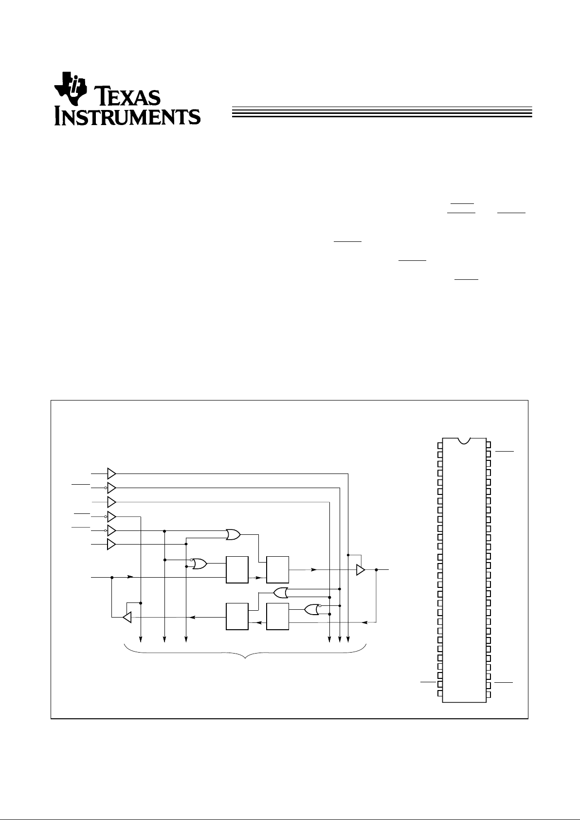
These 18-bit universal bus transceivers can be operated in
transparent, latched, or clock modes by combining D-type
latches and D-type flip-flops. Data flow in each direction is
controlled by output-enable (OEAB and
OEBA), latch enable
(LEAB and LEBA), and clock inputs (
CLKAB and CLKBA)
inputs.ForA-to-Bdataflow,thedeviceoperatesintransparent
mode when LEAB is HIGH. When LEAB is LOW,the A data is
latched if
CLKAB is held at a HIGH or LOW logic level. If LEAB
is LOW, the A bus data is stored in the latch/flip-flop on the
HIGH-to-LOWtransitionof
CLKAB.OEABperformsthe output
enable function on the B port. Data flow from B-to-A is similar
to that of A-to-B and is controlled by
OEBA, LEBA, and
CLKBA. The output buffers are designed with power-off
disable feature that allows live insertion of boards.
The CY74FCT16500T is ideally suited for driving
high-capacitance loads and low-impedance backplanes.
The CY74FCT162500T has 24-mA balanced output drivers
with current limiting resistors in the outputs. This reduces the
need for external terminating resistors and provides for
minimal undershoot and reduced ground bounce. The
CY74FCT162500T is ideal for driving transmission lines.
GND
LogicBlock Diagram Pin Configuration
1
2
3
4
5
6
7
8
9
10
11
12
33
32
31
30
29
36
35
OEAB
34
SSOP/TSSOP
Top View
13
14
15
16
17
18
19
20
21
22
23
24
45
44
43
42
41
37
38
39
40
48
47
46
LEAB
A
1
A
2
A
3
B
1
B
2
B
3
GND
GND
GND
V
CC
A
6
A
7
A
4
A
5
B
4
B
5
B
6
B
7
V
CC
GND
A
10
A
11
A
8
A
9
B
8
B
9
B
11
B
12
GND
A
12
V
CC
A
16
GND
A
14
V
CC
A
15
A
17
FCT16500-1
TO 17 OTHER CHANNELS
LEAB
OEBA
LEBA
CLKAB
CLKBA
OEAB
C
D
C
D
C
D
C
D
A
1
B
1
25
26
27
28
49
52
51
50
A
13
OEBA
LEBA
GND
A
18
CLKAB
53
56
55
54
B
10
GND
B
14
B
15
B
13
B
16
B
17
GND
B
18
CLKBA
FCT16500-2

CY74FCT16500T
CY74FCT162500T
2
Maximum Ratings
[5, 6]
(Above which the useful life may be impaired. For user
guidelines, not tested.)
Storage Temperature .......................Com’l −55°C to +125°C
Ambient Temperature with
Power Applied...................................Com’l −55°C to +125°C
DC Input Voltage .................................................−0.5V to +7.0V
DC Output Voltage..............................................−0.5V to +7.0V
DC Output Current
(Maximum Sink Current/Pin)...........................−60 to +120 mA
Power Dissipation..........................................................1.0W
Static Discharge Voltage............................................>2001V
(per MIL-STD-883, Method 3015)
Pin Summary
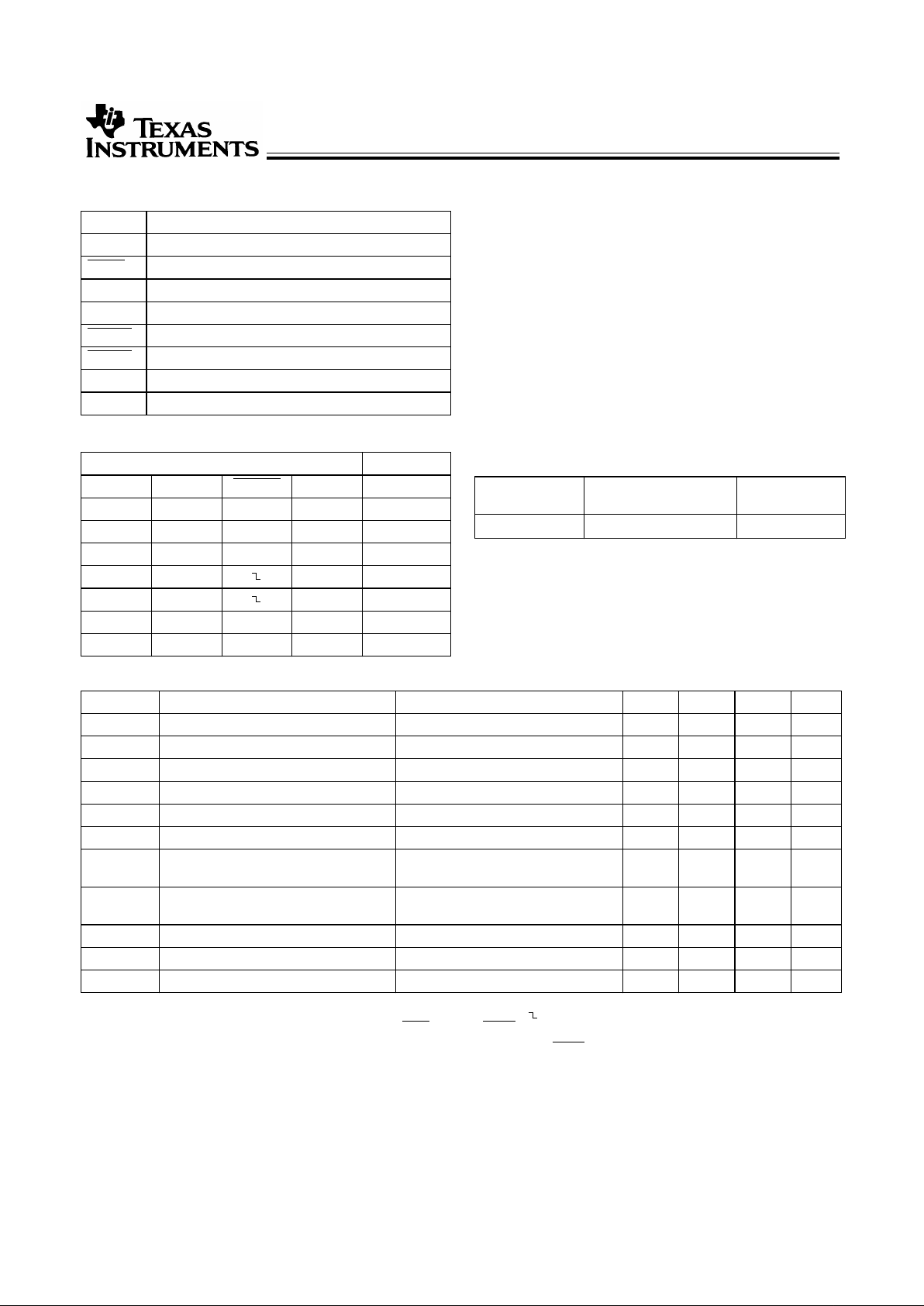
Name Description
OEAB A-to-B Output Enable Input
OEBA B-to-A Output Enable Input (Active LOW)
LEAB A-to-B Latch Enable Input
LEBA B-to-A Latch Enable Input
CLKAB A-to-B Clock Input (Active LOW)
CLKBA B-to-A Clock Input (Active LOW)
A A-to-B Data Inputs orB-to-A Three-State Outputs
B B-to-A Data Inputs orA-to-B Three-State Outputs
Function Table
[1, 2]
Inputs Outputs
OEAB LEAB CLKAB A B
L X X X Z
H H X L L
H H X H H
H L L L
H L H H
H L H X B
[3]
H L L X B
[4]
Operating Range
Range
Ambient
Temperature V
CC
Industrial −40°C to +85°C 5V ± 10%
Electrical Characteristics Over the Operating Range
Parameter Description Test Conditions Min. Typ.
[7]
Max. Unit
V
IH
Input HIGH Voltage 2.0 V
V
IL
Input LOW Voltage 0.8 V
V
H
Input Hysteresis
[8]
100 mV
V
IK
Input Clamp Diode Voltage VCC=Min., IIN=−18 mA −0.7 −1.2 V
I
IH
Input HIGH Current VCC=Max., VI=V
CC
±1 µA
I
IL
Input LOW Current VCC=Max., VI=GND. ±1 µA
I
OZH
High Impedance Output Current
(Three-State Output pins)
VCC=Max., V
OUT
=2.7V ±1 µA
I
OZL
High Impedance Output Current
(Three-State Output pins)
VCC=Max., V
OUT
=0.5V ±1 µA
I
OS
Short Circuit Current
[9]
VCC=Max., V
OUT
=GND −80 −140 −200 mA
I
O
Output Drive Current
[9]
VCC=Max., V
OUT
=2.5V −50 −180 mA
I
OFF
Power-Off Disable VCC=0V, V
OUT
≤4.5V
[10]
±1 µA
Notes:
1. H = HIGH Voltage Level. L = LOW Voltage Level. X = Don’t Care. Z = HIGH Impedance. = HIGH-to-LOW Transition.
2. A-to-B data flow is shown, B-to-A data flow is similar but uses
OEBA, LEBA, and CLKBA.
3. Output level before the indicated steady-state input conditions were established.
4. Output level before the indicated steady-state input conditions were established, provided that CLKAB was LOW before LEAB went LO W.
5. Operation beyondthe limits set forth mayimpair the useful life of the device. Unless otherwise noted, these limits are over the operating free-air temperature
range.
6. Unused inputs must always be connected to an appropriate logic voltage level, preferably either VCC or ground.
7. Typical values are at VCC= 5.0V , TA= +25˚C ambient.
8. This parameter is specified but not tested.
9. Not more than oneoutput should be shorted at a time. Duration of short should not exceed onesecond. The use of high-speed test apparatus and/or sample
and hold techniquesare preferable in order to minimize internal chip heating and more accurately reflect operational values.Otherwise prolonged shorting of
a high output may raise the chip temperature well above normal and thereby cause invalid readings in other parametric tests. In any sequence of parameter
tests, IOS tests should be performed last.
10. Tested at +25˚C.
 Loading...