

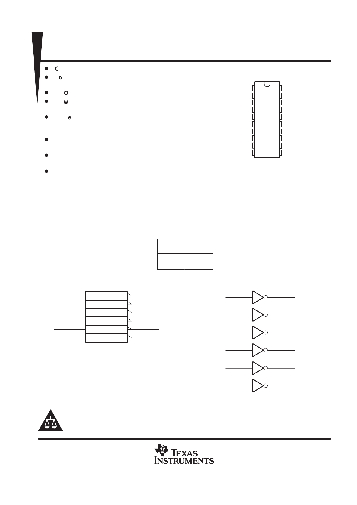
CDC204
HEX INVERTER/CLOCK DRIVER
SCAS098E – OCTOBER 1989– REVISED OCTOBER 1998
1
POST OFFICE BOX 655303 • DALLAS, TEXAS 75265
D
CDC204 Replaces 74AC11204
D
Low-Skew Propagation Delay
Specifications for Clock-Driver Applications
D
CMOS-Compatible Inputs and Outputs
D
Flow-Through Architecture Optimizes
PCB Layout
D
Center-Pin VCC and GND Pin
Configurations Minimize High-Speed
Switching Noise
D
EPIC
(Enhanced-Performance Implanted
CMOS) 1-µm Process
D
500-mA Typical Latch-Up Immunity at
125°C
D
Package Options Include Plastic
Small-Outline Package (DW))
description
The CDC204 contains six independent inverters. The device performs the Boolean function Y = A. It is designed
specifically for applications requiring low skew between switching outputs.
The CDC204 is characterized for operation from T
A
= 25°C to 70°C.
FUNCTION TABLE
INPUT
A
OUTPUT
Y
H L
L H
logic symbol
†
logic diagram (positive logic)
1A
20
20
1A
1Y
1
19
2A
2Y
2
18
3A
3Y
3
13
4A
4Y
8
12
5A
5Y
9
11
6A
6Y
10
1
1Y
1
2A
19
2Y
2
3A
18
3Y
3
4A
13
4Y
8
5A
12
5Y
9
6A
11
6Y
†
This symbol is in accordance with ANSI/IEEE Std 91-1984
and IEC Publication 617-12.
10
Copyright 1998, Texas Instruments Incorporated
PRODUCTION DATA information is current as of publication date.
Products conform to specifications per the terms of Texas Instruments
standard warranty. Production processing does not necessarily include
testing of all parameters.
EPIC is a trademark of Texas Instruments Incorporated.
Please be aware that an important notice concerning availability, standard warranty, and use in critical applications of
Texas Instruments semiconductor products and disclaimers thereto appears at the end of this data sheet.
1
2
3
4
5
6
7
8
9
10
20
19
18
17
16
15
14
13
12
11
1Y
2Y
3Y
GND
GND
GND
GND
4Y
5Y
6Y
1A
2A
3A
NC
V
CC
V
CC
NC
4A
5A
6A
DW PACKAGE
(TOP VIEW)
NC – No internal connection
CDC204
HEX INVERTER/CLOCK DRIVER
SCAS098E – OCTOBER 1989– REVISED OCTOBER 1998
2
POST OFFICE BOX 655303 • DALLAS, TEXAS 75265
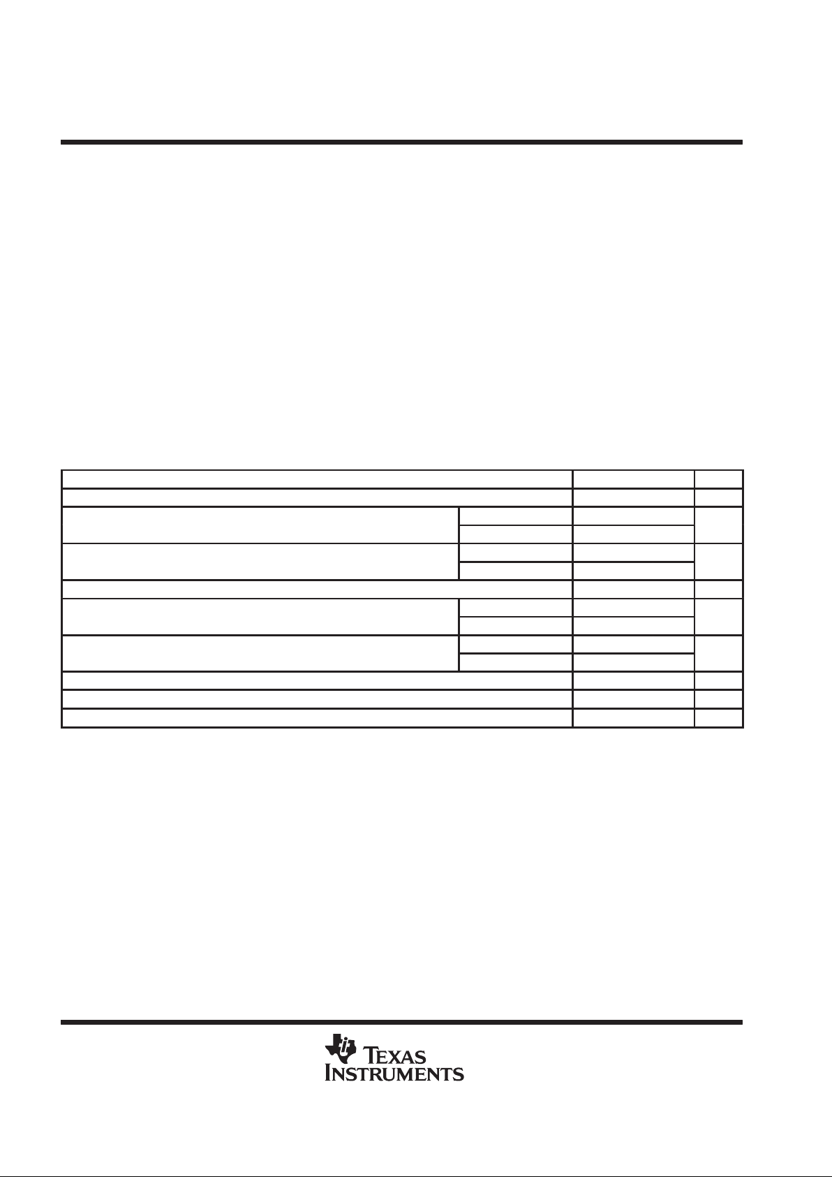
absolute maximum ratings over operating free-air temperature range (unless otherwise noted)
†
Supply voltage range, VCC –0.5 V to 7 V. . . . . . . . . . . . . . . . . . . . . . . . . . . . . . . . . . . . . . . . . . . . . . . . . . . . . . . . . .
Input voltage range, V
I
(see Note 1) –0.5 V to VCC + 0.5 V. . . . . . . . . . . . . . . . . . . . . . . . . . . . . . . . . . . . . . . . . .
Output voltage range, V
O
(see Note 1) –0.5 V to VCC + 0.5 V. . . . . . . . . . . . . . . . . . . . . . . . . . . . . . . . . . . . . . .
Input clamp current, I
IK
(VI < 0 or VI > VCC) ±20 mA. . . . . . . . . . . . . . . . . . . . . . . . . . . . . . . . . . . . . . . . . . . . . . . .
Output clamp current, I
OK
(VO < 0 or VO > VCC) ±50 mA. . . . . . . . . . . . . . . . . . . . . . . . . . . . . . . . . . . . . . . . . . . .
Continuous output current, I
O
(VO = 0 to VCC) ±50 mA. . . . . . . . . . . . . . . . . . . . . . . . . . . . . . . . . . . . . . . . . . . . . .
Continuous current through V
CC
or GND ±150 mA. . . . . . . . . . . . . . . . . . . . . . . . . . . . . . . . . . . . . . . . . . . . . . . . . .
Maximum power dissipation at T
A
= 55°C (in still air) (see Note 2) 1.6 W. . . . . . . . . . . . . . . . . . . . . . . . . . . . . . .
Storage temperature range, T
stg
–65°C to 150°C. . . . . . . . . . . . . . . . . . . . . . . . . . . . . . . . . . . . . . . . . . . . . . . . . . .
†
Stresses beyond those listed under “absolute maximum ratings” may cause permanent damage to the device. These are stress ratings only, and
functional operation of the device at these or any other conditions beyond those indicated under “recommended operating conditions” is not
implied. Exposure to absolute-maximum-rated conditions for extended periods may affect device reliability.
NOTES: 1. The input and output negative-voltage ratings may be exceeded if the input and output clamp-current ratings are observed.
2. The maximum package power dissipation is calculated using a junction temperature of 150°C and a board trace length of 750 mils.
For more information, refer to the
Package Thermal Considerations
application note in the 1994
ABT Advanced BiCMOS T echnology
Data Book
, literature number SCBD002B.
recommended operating conditions
MIN NOM MAX UNIT
V
CC
Supply voltage 4.75 5 5.25 V
p
VCC = 4.75 V 3.3
VIHHigh-level input voltage
VCC = 5.25 V 3.7
V
p
VCC = 4.75 V 1.4
VILLow-level input voltage
VCC = 5.25 V 1.6
V
V
I
Input voltage 0 V
CC
V
p
VCC = 4.75 V –24
IOHHigh-level output current
VCC = 5.25 V –24
mA
p
VCC = 4.75 V 24
IOLLow-level output current
VCC = 5.25 V 24
mA
∆t/∆v Input transition rise or fall rate 0 10 ns/V
f
clock
Input clock frequency 80 MHz
T
A
Operating free-air temperature 25 70 °C
CDC204
HEX INVERTER/CLOCK DRIVER
SCAS098E – OCTOBER 1989– REVISED OCTOBER 1998
3
POST OFFICE BOX 655303 • DALLAS, TEXAS 75265
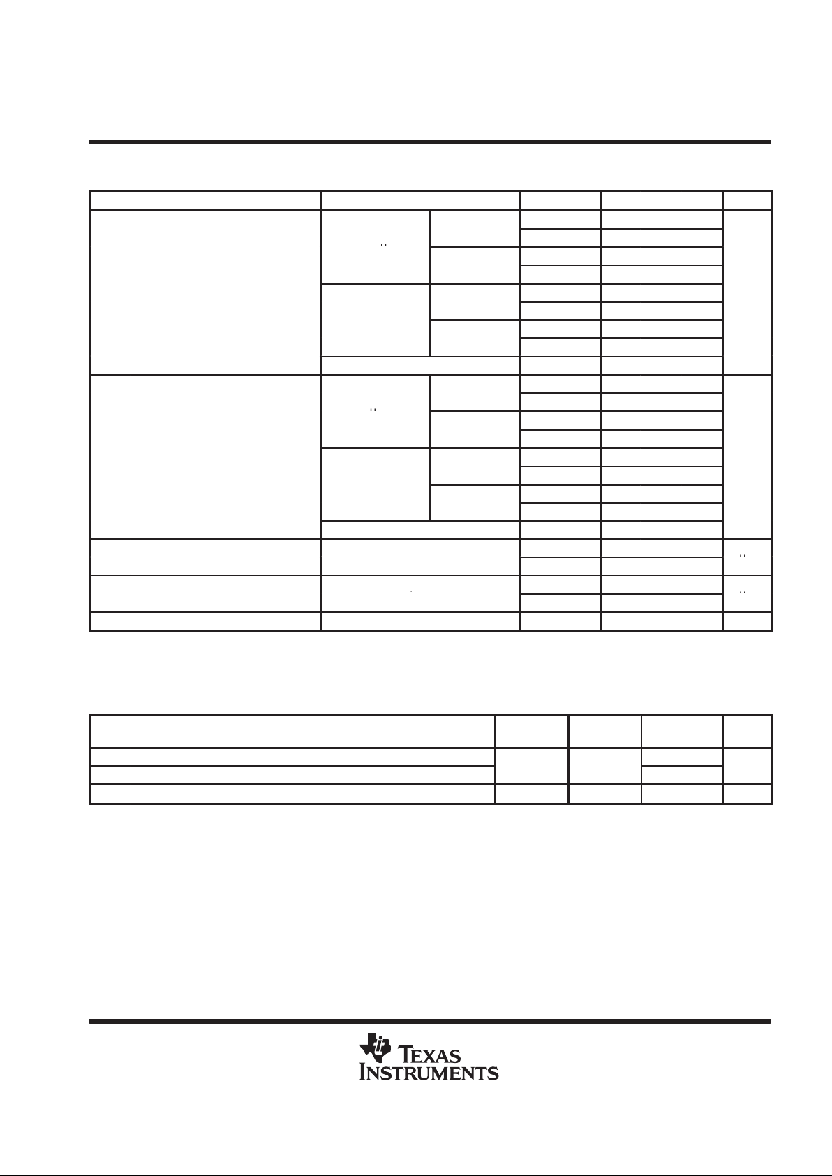
electrical characteristics over recommended operating free-air temperature range (unless
otherwise noted)
PARAMETER TEST CONDITIONS
T
A
†
MIN TYP MAX UNIT
25°C 4.65
V
CC
= 4.75
V
Full range 4.65
I
OH
= –50 µ
A
25°C 5.15
V
CC
= 5.25
V
Full range 5.15
V
OH
High-level voltage output
25°C 4.19
V
V
CC
= 4.75
V
Full range 4.05
I
OH
= –
24 mA
25°C 4.68
V
CC
=
5.25 V
Full range 4.55
IOH = –75 mA‡, VCC = 5.25 V Full range 3.6
25°C 0.1
V
CC
= 4.75
V
Full range 0.1
I
OL
= 50 µ
A
25°C 0.1
V
CC
=
5.25 V
Full range 0.1
V
OL
Low-level voltage output
25°C 0.36
V
V
CC
=
4.75 V
Full range 0.44
I
OL
= 24
mA
25°C 0.36
V
CC
= 5.25
V
Full range 0.44
IOL = 75 mA‡, VCC = 5.25 V Full range 1.65
p
25°C ±0.1
IIInput current
V
I
=
V
CC
or
GND
V
CC
= 5.25
V
Full range ±1
µ
A
pp
V
= V
or GND,
VCC = 5.25 V ,
25°C 4
ICCSupply current
ICC
,
IO = 0
Full range 40
µ
A
C
i
Input capacitance VI = VCC or GND, VCC = 5 V 25°C 4 pF
†
Full range is TA = 25°C to 70°C.
‡
Not more than one output should be tested at a time, and the duration of the test should not exceed 10 ms.
switching characteristics over recommended operating free-air temperature range,
V
CC
= 5 V ± 0.25 V (see Note 3 and Figures 1 and 2)
PARAMETER
FROM
(INPUT)TO(OUTPUT)
MIN MAX UNIT
t
PLH
Propagation delay time, low-to-high level (see Figure 1)
3.7 5.7
t
PHL
Proagation delay time, high-to-low level (see Figure 1)
A
Y
2.9 5.7
ns
t
sk(o)
Output skew time (see Figure 2) A Y 1 ns
NOTE 3: All specifications are valid only for all outputs switching simultaneously and in phase.
 Loading...