

Texas Instruments bq25120A Datasheet
GND
HOST
SDA
SCL
INT
SW
BAT
MR
BQ2512x
MCU /
SYSTEM
-+
NTC
TS
LS / LDO
<100mA
Load
IN
SYS
RESET
LSCTRL
VINLS
Unregulated
Load
PMID
PG
IPRETERM
ISET
ILIM
CD
IN
Copyright © 2016, Texas Instruments Incorporated
Product
Folder
Order
Now
Technical
Documents
Tools &
Software
Support &
Community
bq25120A
SLUSD08A –MAY 2017–REVISED JANUARY 2018
bq25120A Low IQHighly Integrated Battery Charge Management Solution for Wearables
and IoT
1 Features
1
• Increases System Operation Time Between
Charges
– Configurable 300-mA Buck Regulator
(1.8-V Default)
– 700 nA (typical) Iq with Buck Converter
Enabled (No Load)
– Configurable Load Switch or 100mA LDO
Output (Load Switch by Default)
– Up to 300-mA Charge Current for Fast
Charging
– 0.5% Accurate Battery Voltage Regulation
(Configurable from 3.6 V to 4.65 V in 10-mV
Steps)
– Configurable Termination Current Down to
500 µA
– Simple Voltage Based Battery Monitor
• Highly Integrated Solution with Small Footprint
– 2.5 mm x 2.5 mm WCSP Package and 6
External Components for Minimal Solution
– Push-Button Wake-Up and Reset with
Adjustable Timers
– Power Path Management for Powering the
System and Charging the Battery
– Power Path Management enables <50 nA Ship
Mode Battery Quiescent Current for Longest
Shelf Life
– Battery Charger Operates from 3.4 V – 5.5 V
(5.5-V OVP / 20-V Tolerant)
– Dedicated Pins for Input Current Limit, Charge
Current, Termination Current, and Status
Output
• I2C Communication Control
– Charge Voltage and Current
1
– Termination Threshold
– Input Current Limit
– VINDPM Threshold
– Timer Options
– Load Switch Control
– Controls for Interrupts for Faults and Status
– System Output Voltage Adjustment
– LDO Output Voltage Adjustment
An IMPORTANT NOTICE at the end of this data sheet addresses availability, warranty, changes, use in safety-critical applications,
intellectual property matters and other important disclaimers. PRODUCTION DATA.
2 Applications
• Smart Watches and other Wearable Devices
• Fitness Accessories
• Health Monitoring Medical Accessories
• Rechargeable Toys
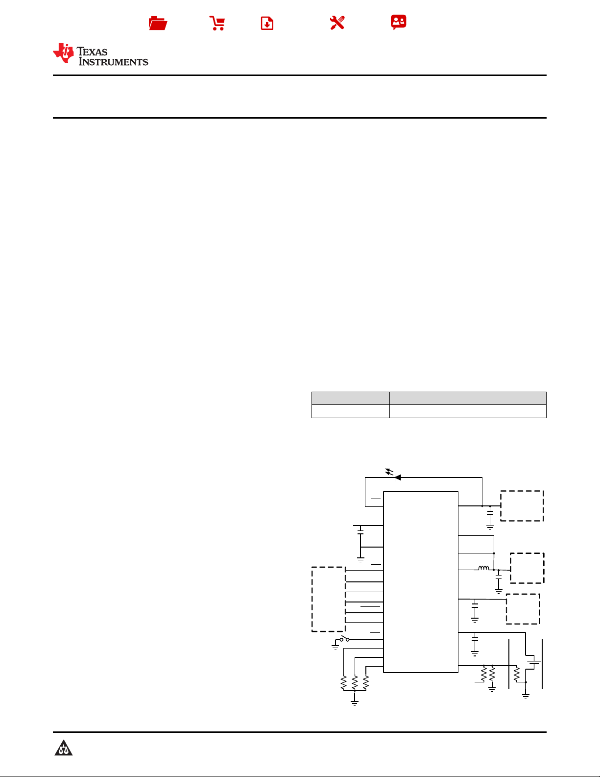
3 Description
The bq25120A is a highly integrated battery charge
management IC that integrates the most common
functions for wearable devices: Linear charger,
regulated output, load switch, manual reset with
timer, and battery voltage monitor. The integrated
buck converter is a high efficiency, low IQswitcher
using DCS control that extends light load efficiency
down to 10-µA load currents. The low quiescent
current during operation and shutdown enables
maximum battery life. The device supports charge
currents from 5 mA to 300 mA. The input current
limit, charge current, buck converter output voltage,
LDO output voltage, and other parameters are
programmable through the I2C interface.
Device Information
PART NUMBER PACKAGE BODY SIZE (NOM)
BQ25120A DSBGA (25) 2.50 mm x 2.50 mm
(1) For all available packages, see the orderable addendum at
the end of the data sheet.
Simplified Schematic
IN
(1)

bq25120A
SLUSD08A –MAY 2017–REVISED JANUARY 2018
www.ti.com
Table of Contents
1 Features.................................................................. 1
2 Applications ........................................................... 1
3 Description ............................................................. 1
4 Revision History..................................................... 2
5 Description (continued)......................................... 3
6 Device Comparison Table..................................... 3
7 Pin Configuration and Functions......................... 4
8 Specifications......................................................... 6
8.1 Absolute Maximum Ratings ...................................... 6
8.2 ESD Ratings.............................................................. 6
8.3 Recommended Operating Conditions....................... 6
8.4 Thermal Information.................................................. 7
8.5 Electrical Characteristics........................................... 8
8.6 Timing Requirements ............................................. 12
8.7 Typical Characteristics............................................ 15
9 Detailed Description............................................ 17
9.1 Overview ................................................................. 17
9.2 Functional Block Diagram....................................... 17
9.3 Feature Description................................................. 18
9.4 Device Functional Modes........................................ 31
9.5 Programming .......................................................... 33
9.6 Register Maps ........................................................ 36
10 Application and Implementation........................ 47
10.1 Application Information.......................................... 47
10.2 Typical Application ............................................... 47
11 Power Supply Recommendations ..................... 62
12 Layout................................................................... 63
12.1 Layout Guidelines ................................................. 63
12.2 Layout Example .................................................... 63
13 Device and Documentation Support................. 64
13.1 Device Support...................................................... 64
13.2 Trademarks........................................................... 64
13.3 Electrostatic Discharge Caution............................ 64
13.4 Glossary................................................................ 64
14 Mechanical, Packaging, and Orderable
Information........................................................... 64
4 Revision History
NOTE: Page numbers for previous revisions may differ from page numbers in the current version.
Changes from Original (May 2017) to Revision A Page
• Changed expression terms in Equation 3 and Equation 4 for clarification........................................................................... 26
2
Submit Documentation Feedback Copyright © 2017–2018, Texas Instruments Incorporated
Product Folder Links: bq25120A
bq25120A
www.ti.com
SLUSD08A –MAY 2017–REVISED JANUARY 2018
5 Description (continued)
The battery is charged using a standard Li-Ion charge profile with three phases: precharge, constant current and
constant voltage. A voltage-based JEITA compatible battery pack thermistor monitoring input (TS) is included
that monitors battery temperature and automatically changes charge parameters to prevent the battery from
charging outside of its safe temperature range. The charger is optimized for 5-V USB input, with 20-V tolerance
to withstand line transients. The buck converter is run from the input or battery. When in battery only mode, the
device can run from a battery up to 4.65 V.
A configurable load switch allows system optimization by disconnecting infrequently used devices. The manual
reset with timer allows mutliple different configuration options for wake are reset optimization.
6 Device Comparison Table
PART NUMBER VINDPM
BQ25120A Enabled 1.8V Load Switch 4.2 V 10 mA 2 mA Off
DEFAULT SYS
OUTPUT
DEFAULT LDO
OUTPUT
DEFAULT
VBERG
DEFAULT
CHARGE
CURRENT
DEFAULT
TERMINATION
CURRENT
DEFAULT SHIP
MODE
Product Folder Links: bq25120A
Submit Documentation FeedbackCopyright © 2017–2018, Texas Instruments Incorporated
3
GND
RESETINT
/MR
IPRETE
RM
ISET
BATBAT
TS
ILIM
/PG
VINLS
VINLS
PGNDSWPMID
A
B
C
D
1 2 3 4
SDALSCTRL/CD SCL
E
IN
LS/LDO
SYSPMID
GND
5
bq25120A
SLUSD08A –MAY 2017–REVISED JANUARY 2018
7 Pin Configuration and Functions
www.ti.com
YFP Package
25-Pin DSBGA
Top View
Pin Functions
PIN
NAME NO.
IN A2 I
PMID A3, B3 I/O
GND A1, D5 Ground connection. Connect to the ground plane of the circuit.
PGND A5
CD E2 I
SDA E4 I/O I2C Interface Data. Connect SDA to the logic rail through a 10-kΩ resistor.
SCL E5 I I2C Interface Clock. Connect SCL to the logic rail through a 10-kΩ resistor.
ILIM C2 I
LSCTRL E3 I
ISET C1 I
I/O DESCRIPTION
DC Input Power Supply. IN is connected to the external DC supply. Bypass IN to GND with
at least 1 µF of capacitance using a ceramic capacitor.
High Side Bypass Connection. Connect at least 3µF of ceramic capacitance with DC bias
derating from PMID to GND as close to the PMID and GND pins as possible. When entering
Ship Mode, PMID is discharged by a 20-kΩ internal discharge resistor.
Power ground connection. Connect to the ground plane of the circuit. Connect the output
filter cap from the buck converter to this ground as shown in the layout example.
Chip Disable. Drive CD low to place the part in High-Z mode with battery only present, or
enable charging when VINis valid. Drive CD high for Active Battery mode when battery only
is present, and disable charge when VINis present. CD is pulled low internally with 900 kΩ.
Adjustable Input Current Limit Programming. Connect a resistor from ILIM to GND to
program the input current limit. The input current includes the system load and the battery
charge current. Connect ILIM to GND to set the input current limit to the internal default
threshold. ILIM can also be updated through I2C.
Load Switch and LDO Control Input. Pull high to enable the LS/LDO output, pull low to
disable the LS/LDO output.
Fast-Charge Current Programming Input. Connect a resistor from ISET to GND to program
the fast-charge current level. Connect a resistor from ISET to GND to set the charge current
to the internal default. ISET can also be updated through I2C. While charging, the voltage at
ISET reflects the actual charging current and can be used to monitor charge current if an
ISET resistor is present and the device is not in host mode.
4
Submit Documentation Feedback Copyright © 2017–2018, Texas Instruments Incorporated
Product Folder Links: bq25120A
www.ti.com
SLUSD08A –MAY 2017–REVISED JANUARY 2018
Pin Functions (continued)
PIN
NAME NO.
IPRETERM D1 I
INT D2 O
PG D4 O
RESET D3 O
MR E1 I
SW A4 O Inductor Connection. Connect to the switched side of the external inductor.
SYS B5 I
LS/LDO C5 O
VINLS B4, C4 I
BAT B1, B2 I/O
TS C3 I
I/O DESCRIPTION
Termination current programming input. Connect a 0-Ω to 10-kΩ resistor from IPRETERM to
GND to program the termination current between 5% and 20% of the charge current. The
pre-charge current is the same as the termination current setting. Connect IPRETERM to
GND to set the termination current to the internal default threshold. IPRETERM can also be
updated through I2C.
Status Output. INT is an open-drain output that signals charging status and fault interrupts.
INT pulls low during charging. INT is high impedance when charging is complete, disabled,
or the charger is in high impedance mode. When a fault occurs, a 128µs pulse is sent out as
an interrupt for the host. INT charge indicator function is enabled/disabled using the EN_INT
bit in the control register. Connect INT to a logic rail using an LED for visual indication of
charge status or through a 100kΩ resistor to communicate with the host processor.
Open-drain Power Good status indication output. PG pulls to GND when VINis above V
+ V
and less that V
SLP
specified limits. Connect PG to the desired logic voltage rail using a 1kΩ to 100kΩ resistor,
or use with an LED for visual indication. PG can also be configured as a push-button voltage
shifted output (MRS) in the registers, where the output of the PG pin reflects the status of the
MR input, but pulled up to the desired logic voltage rail using a 1kΩ to 100kΩ resistor.
Reset Output. RESET is an open drain active low output that goes low when MR is held low
for longer than t
deasserted after the t
Manual Reset Input. MR is a push-button input that must be held low for greater than t
to assert the reset output. If MR is pressed for a shorter period, there are two programmable
timer events, t
be used to bring the device out of Ship mode.
System Voltage Sense Connection. Connect SYS to the system output at the output bulk
capacitors. Bypass SYS locally with at least 4.7 µF of effective ceramic capacitance.
Load Switch or LDO output. Connect 1 µF of effective ceramic capacitance to this pin to
assure stability. Be sure to account for capacitance bias voltage derating when selecting the
capacitor.
Input to the Load Switch / LDO output. Connect 1 µF of effective ceramic capacitance from
this pin to GND.
Battery Connection. Connect to the positive terminal of the battery. Bypass BAT to GND with
at least 1 µF of ceramic capacitance.
Battery Pack NTC Monitor. Connect TS to the center tap of a resistor divider from VIN to
GND. The NTC is connected from TS to GND. The TS function provides four thresholds for
JEITA compatibility. TS faults are reported by the I2C interface during charge mode.
. PG is high-impedance when the input power is not within
OVP
, which is configurable by the MRRESET registers. RESET is
RESET
WAKE1
RESET_D,
and t
typically 400ms.
, that trigger an interrupt to the host. The MR input can also
WAKE2
bq25120A
(BAT)
RESET
Product Folder Links: bq25120A
Submit Documentation FeedbackCopyright © 2017–2018, Texas Instruments Incorporated
5
bq25120A
SLUSD08A –MAY 2017–REVISED JANUARY 2018
www.ti.com
8 Specifications
8.1 Absolute Maximum Ratings
over operating free-air temperature range (unless otherwise noted)
IN wrt GND –0.3 20 V
Input voltage
Output voltage SYS 3.6 V
Input current IN 400 mA
Sink current INT 10 mA
Sink/Source Current RESET 10 mA
Output Voltage Continuos SW –0.7 7.7 V
Output Current Continuous
Current LS/LDO 150 mA
BAT Operating Voltage VBAT, MR, 6.6 V
Junction Temperature –40 125 °C
Storage Temperature, T
stg
(1) Stresses beyond those listed under Absolute Maximum Ratings may cause permanent damage to the device. These are stress ratings
only, which do not imply functional operation of the device at these or any other conditions beyond those indicated under Recommended
Operating Conditions. Exposure to absolute-maximum-rated conditions for extended periods may affect device reliability.
PMID, VINLS wrt GND –0.3 7.7 V
CD, SDA, SCL, ILIM, ISET, IPRETERM, LSCTRL,
INT, RESET, TS
SW 400 mA
SYS, BAT 300 mA
(1)
MIN MAX UNIT
wrt GND –0.3 5.5 V
300 °C
8.2 ESD Ratings
VALUE UNIT
(1)
±2000
±500
V
(ESD)
Electrostatic discharge
Human body model (HBM), per ANSI/ESDA/JEDEC JS-001
Charged device model (CDM), per JEDEC specification JESD22-
(2)
C101
(1) JEDEC document JEP155 states that 500-V HBM allows safe manufacturing with a standard ESD control process.
(2) JEDEC document JEP157 states that 250-V CDM allows safe manufacturing with a standard ESD control process.
8.3 Recommended Operating Conditions
over operating free-air temperature range (unless otherwise noted)
MIN NOM MAX UNIT
V
IN
V
(BAT)
V
(VINLS)
V
(VINLS)
I
IN
I
(SW)
I
(PMID)
ILS/LDO Output Current from LS/LDO 100 mA
I
, I
(BAT)
T
J
(1) Any voltage greater than shown should be a transient event.
(2) These inputs will support 6.6 V for less than 10% of the lifetime at V
IN voltage range 3.4 5 20
IN operating voltage range, recommended 3.4 5 5.5
V
operating voltage range 5.5
(BAT)
VINLS voltage range for Load Switch 0.8 5.5
VINLS voltage range for LDO 2.2 5.5 V
Input Current, IN input 400 mA
Output Current from SW, DC 300 mA
Output Current from PMID, DC 300 mA
Charging and discharging using internal battery FET 300 mA
(SYS)
Operating junction temperature range –40 125 °C
or VIN, with a reduced current and/or performance.
(BAT)
(1)
(2)
V
V
V
V
6
Submit Documentation Feedback Copyright © 2017–2018, Texas Instruments Incorporated
Product Folder Links: bq25120A
bq25120A
www.ti.com
SLUSD08A –MAY 2017–REVISED JANUARY 2018
8.4 Thermal Information
bq25120A
THERMAL METRIC
R
θJA
R
θJC(top)
R
θJB
ψ
JT
ψ
JB
R
θJC(bot)
Junction-to-ambient thermal resistance 60 °C/W
Junction-to-case (top) thermal resistance 0.3 °C/W
Junction-to-board thermal resistance 12.0 °C/W
Junction-to-top characterization parameter 1.2 °C/W
Junction-to-board characterization parameter 12.0 °C/W
Junction-to-case (bottom) thermal resistance N/A °C/W
(1) For more information about traditional and new thermal metrics, see the Semiconductor and IC Package Thermal Metrics application
report.
(1)
UNITYFP (DSBGA)
25 PINS
Product Folder Links: bq25120A
Submit Documentation FeedbackCopyright © 2017–2018, Texas Instruments Incorporated
7
bq25120A
SLUSD08A –MAY 2017–REVISED JANUARY 2018
8.5 Electrical Characteristics
Circuit of Figure 1, V
otherwise noted)
PARAMETERS TEST CONDITIONS MIN TYP MAX UNIT
INPUT CURRENTS
I
IN
I
(BAT_HIZ)
I
(BAT_ACTIVE)
I
(BAT_SHIP)
POWER-PATH MANAGEMENT and INPUT CURRENT LIMIT
V
DO(IN-PMID)
V
DO(BAT-PMID)
V
(BSUP1)
V
(BSUP2)
I
(BAT_OCP)
I
(ILIM)
K
(ILIM)
V
IN(DPM)
BATTERY CHARGER
V
D(PPM)
R
ON(BAT-PMID)
V
(BATREG)
Supply Current for
Control
Battery discharge current
in High Impedance Mode
Battery discharge current
in Active Battery Mode
Battery discharge current
in Ship Mode
VIN– V
V
(BAT)
Enter supplement mode
threshold
Exit supplement mode
threshold
Current Limit, Discharge
Mode
Input Current Limit Programmable Range, 50-mA steps 50 400 mA
Maximum Input Current
using ILIM
I
accuracy I
ILIM
accuracy
Maximum input current
factor
Input voltage threshold
when input current is
reduced
V
IN_DPM
accuracy
PMID voltage threshold
when charge current is
reduced
Internal Battery Charger
MOSFET on-resistance
Charge Voltage
Voltage Regulation
Accuracy
(UVLO)
(PMID)
– V
(PMID)
threshold
< VIN< V
ILIM
and VIN> V
(OVP)
V
< VIN< V
(UVLO)
Switching, –40°C < TJ< 85°C
V
< VIN< V
(UVLO)
Switching
0°C < TJ< 85°C, VIN= 5 V, Charge Disabled 1.5 mA
0°C < TJ< 60°C, VIN= 0 V, High-Z Mode, PWM Not
Switching, V
0°C < TJ< 60°C, VIN= 0 V, High-Z Mode, PWM Not
Switching, V
0°C < TJ< 60°C, VIN= 0 V or floating, High-Z Mode, PWM
Switching, No Load
0°C < TJ< 85°C, VIN= 0 V, High-Z Mode, PWM Switching,
LSLDO enabled
0°C < TJ< 85°C, VIN= 0 V, Active Battery Mode, PWM
Switching, LSLDO enabled, I2C Enabled, V
4.65 V
0°C < TJ< 85°C, 0 < VIN< V
PWM Switching, LSLDO disabled, I2C Enabled, CD = Low,
V
< V
(BUVLO)
0°C < TJ< 85°C, VIN= 0 V, Ship Mode 2 150 nA
VIN= 5 V, IIN= 300 mA 125 170 mV
VIN= 0 V, V
V
> V
(BAT)
(BUVLO)
V
> V
(BAT)
(BUVLO)
V
> V
(BAT)
(BUVLO)
50 mA to 100 mA –12% 12%
100 mA to 400 mA –5% 5%
I
= 50 mA to 100 mA 175 200 225 AΩ
(ILIM)
I
= 100 mA to 400 mA 190 200 210 AΩ
(ILIM)
Programmable Range using V
disabled using V
Above V
(BATREG)
Measured from BAT to PMID, V
Operating in voltage regulation, Programmable Range, 10-
mV steps
TJ= 25°C –0.5% 0.5%
TJ= 0°C to 85°C –0.5% 0.5%
+ V
, TJ= –40°C to 85°C and TJ= 25°C for typical values (unless
(SLP)
+ V
+ V
(SLP)
(SLP)
PWM
PWM NOT
1 mA
0.7 1.2 µA
0.9 1.5 µA
(BAT)
(BAT)
< 4.65 V
< 6.6 V
(BUVLO)
(BUVLO)
(BAT)
(OVP)
(OVP)
< V
< V
and VIN> V
and VIN> V
(BAT)
(BAT)
0.75 3.5 µA
1.35 4.25 µA
< V
(BUVLO)
, Active Battery Mode,
IN(UVLO)
< 4.65 V
(BAT)
> 3 V, Iff= 400 mA 120 160 mV
(BAT)
(BAT)
<
6.8 12 µA
6.2 11 µA
V
<
(PMID)
V
– 25
(BAT)
mV
V
<
(PMID)
V
–
(BAT)
5mV
0.85 1.15 1.35 A
K
/
(ILIM)
R
(ILIM)
Registers. Can be
IN(DPM_ON)
IN(DPM)
4.2 4.9 V
–3% 3%
0.2 V
= 4.35 V, High-Z mode 300 400 mΩ
(BAT)
3.6 4.65 V
www.ti.com
3 mA
V
V
8
Submit Documentation Feedback Copyright © 2017–2018, Texas Instruments Incorporated
Product Folder Links: bq25120A
www.ti.com
Electrical Characteristics (continued)
bq25120A
SLUSD08A –MAY 2017–REVISED JANUARY 2018
Circuit of Figure 1, V
otherwise noted)
PARAMETERS TEST CONDITIONS MIN TYP MAX UNIT
Fast Charge Current
Range
I
(CHARGE)
K
(ISET)
I
(TERM)
t
DGL(TERM)
I
(PRE_CHARGE)
V
(RCH)
t
DGL(RCHG)
SYS OUTPUT
R
DS(ON_HS)
R
DS(ON_LS)
R
DS(CH_SYS)
I
(LIMF)
I
(LIM_SS)
V
SYS
LS/LDO OUTPUT
V
IN(LS)
V
OUT
V
LDO
ΔV
/ Δ V
OUT
R
DS(ON_LDO)
R
(DSCH_LSLDO)
Fast Charge Current
using ISET
Fast Charge Current
Accuracy
Fast Charge Current
Factor
Termination charge
current
Termination Current using
IPRETERM
Accuracy I
TERM deglitch time Both rising and falling, 2-mV over-drive, t
Pre-charge current
Pre-charge Current using
I
PRETERM
Accuracy –10% 10%
Recharge threshold
voltage
Recharge threshold
deglitch time
MOSFET on-resistance
for SYS discharge
SW Current limit HS 2.2 V < V
SW Current limit LS 2.2 V < V
PMOS switch current limit
during softstart
SYS Output Voltage
Range
Output Voltage Accuracy VIN= 5 V, PFM mode, I
DC Output Voltage Load
Regulation in PWM mode
DC Output Voltage Line
Regulation in PWM mode
Input voltage range for
LS/LDO
Input voltage range for
LS/LDO
DC output accuracy
Output range for LS/LDO Programmable Range, 0.1 V steps 0.8 3.3 V
DC Line regulation V
IN
DC Load regulation 0 mA < I
Load Transient 2 µA to 100 mA, VOUT = 1. 8 V –120 60 mV
FET Rdson V
MOSFET on-resistance
for LS/LDO discharge
(UVLO)
< VIN< V
(OVP)
V
(BATUVLO)
and VIN> V
< V
(BAT)
(BAT)
< V
+ V
(BATREG)
, TJ= –40°C to 85°C and TJ= 25°C for typical values (unless
(SLP)
5 300 mA
K
/
(ISET)
R
(ISET)
–5% 5%
5 mA > I
Termination current programmable range over I2C
I
(CHARGE)
I
(CHARGE)
I
(CHARGE)
I
(CHARGE)
) > 4 mA –10% 10%
(TERM
Pre-charge current programmable range over I2C
Below V
t
= 100 ns typ, V
FALL
PMID = 3.6 V, I
PMID = 3.6 V, I
VIN = 3.6 V, I
> 300 mA 190 200 210 AΩ
(CHARGE)
0.5 37 mA
< 300 mA, R
< 300 mA, R
< 300 mA, R
< 300 mA, R
= 15 kΩ 5 % of I
(ITERM)
= 4.99 kΩ 10 % of I
(ITERM)
= 1.65 kΩ 15 % of I
(ITERM)
= 549 Ω 20 % of I
(ITERM)
, t
RISE
= 100 ns 64 ms
FALL
0.5 37 mA
I
(TERM)
(BATREG)
falling 32 ms
(RCH)
= 150 mA 675 850 mΩ
(SYS)
= 150 mA 300 475 mΩ
(SYS)
= –10 mA into V
OUT
< 5.5 V 450 600 675 mA
(PMID)
< 5.5 V 450 700 850 mA
(PMID)
pin 22 40 Ω
OUT
100 120 140 mV
Current limit is reduced during softstart 80 130 200 mA
Programmable range, 100 mV Steps 1.1 3.3 V
= 10 mA, V
OUT
V
= 2 V, over load range 0.01 %/mA
OUT
V
OUT
= 2 V, I
= 100 mA, over VINrange 0.01 %/V
OUT
= 1.8 V –2.5% 0 2.5%
(SYS)
Load Switch Mode 0.8 6.6 V
LDO Mode 2.2 6.6 V
TJ= 25°C –2% ±1% 2%
Over VIN, I
OUT(NOM)
(VINLS)
1.7 V < V
, temperature –3% ±2% 3%
OUT
+ 0.5 V < VIN< 6.6 V, I
< 100 mA –1% 1%
OUT
= 5 mA –1% 1%
OUT
= 3.6 V 460 600 mΩ
(VINLS)
< 6.6 V, I
= –10 mA 20 Ω
LOAD
A
SET
SET
SET
SET
A
Product Folder Links: bq25120A
Submit Documentation FeedbackCopyright © 2017–2018, Texas Instruments Incorporated
9
bq25120A
SLUSD08A –MAY 2017–REVISED JANUARY 2018
Electrical Characteristics (continued)
www.ti.com
Circuit of Figure 1, V
(UVLO)
otherwise noted)
PARAMETERS TEST CONDITIONS MIN TYP MAX UNIT
I
(OCL_LDO)
I
(LS/LDO)
I
IN(LDO)
V
IH(LSCTRL)
V
IL(LSCTRL)
PUSHBUTTON TIMER (MR)
V
IL
R
PU
VBAT MONITOR
V
BMON
BATTERY-PACK NTC MONITOR
V
HOT
V
WARM
V
COOL
V
COLD
TS
OFF
PROTECTION
V
(UVLO)
V
UVLO(HYS)
V
(BUVLO)
V
(BATSHORT)
V
(BATSHORT_HYS)
I
(BATSHORT)
V
(SLP)
V
(SLP_HYS)
V
OVP
t
DGL_OVP
T
SHTDWN
T
HYS
t
DGL_SHTDWN
Output Current Limit –
LDO
Output Current
Quiescent current for
VINLS in LDO mode
OFF-state supply current 0.25 µA
High-level input voltage
for LSCTRL
Low-level input voltage
for LSCTRL
Low-level input voltage V
Internal pull-up resistance 120 kΩ
Battery Voltage Monitor
Accuracy
High temperature
threshold
Warm temperature
threshold
Cool temperature
threshold
Low temperature
threshold
TS Disable threshold VTSrising, 2% VINHysteresis 55 60 %V
IC active threshold
voltage
IC active hysteresis VINfalling from above V
Battery Undervoltage
Lockout threshold Range
Default Battery
Undervoltage Lockout
Accuracy
Battery short circuit
threshold
Hysteresis for V
Battery short circuit
charge current
Sleep entry threshold,
VIN– V
(BAT)
Sleep-mode exit
hysteresis
Maximum Input Supply
OVP threshold voltage
Deglitch time, VIN OVP
falling
Thermal trip VIN> V
Thermal hysteresis VIN> V
Deglitch time, Thermal
shutdown
< VIN< V
(BATSHORT)
and VIN> V
(OVP)
V
= 275 365 475 mA
LS/LDO
V
= 3.6 V, V
(VINLS)
V
= 3.3 V, V
(VINLS)
V
= 2.2 V, V
(VINLS)
+ V
(BAT)
= 3.3 V 100 mA
LSLDO
= 0.8 V 100 mA
LSLDO
= 0.8 V 10 mA
LSLDO
, TJ= –40°C to 85°C and TJ= 25°C for typical values (unless
(SLP)
0.9 µA
1.15 V > V
1.15 V > V
> V
BAT
V
Falling - Including 2% increment –3.5 3.5 %V
(BAT)
(VINLS)
(VINLS)
BUVLO
> 6.6 V
> 6.6 V
0.75 x
V
(SYS)
6.6 V
0.25 x
V
(SYS)
0.3 V
VTSfalling, 1% VINHysteresis 14.5 15 15.2 %V
VTSfalling, 1% VINHysteresis 20.1 20.5 20.8 %V
VTSrising, 1% VINHysteresis 35.4 36 36.4 %V
VTSrising, 1% VINHysteresis 39.3 39.8 40.2 %V
VINrising 3.4 3.6 3.8 V
UVLO
Programmable Range for V
Hysteresis
V
falling –2.5% 2.5%
(BAT)
VBAT falling, 150 mV
(BUVLO)
2.2 3.0 V
150 mV
Battery voltage falling 2 V
100 mV
I
(PRETERM)
2 V < V
VINrising above V
BAT
< V
, VINfalling 65 120 mV
(BATREG)
(SLP)
40 65 100 mV
VINrising, 100 mV hysteresis 5.35 5.55 5.75 V
VINfalling below V
UVLO
UVLO
TJrising above T
, 1V/us 32 ms
OVP
114 °C
11 °C
SHTDWN
4 µs
V
(BATREG)
IN
IN
IN
IN
IN
mA
10
Submit Documentation Feedback Copyright © 2017–2018, Texas Instruments Incorporated
Product Folder Links: bq25120A
www.ti.com
Electrical Characteristics (continued)
bq25120A
SLUSD08A –MAY 2017–REVISED JANUARY 2018
Circuit of Figure 1, V
(UVLO)
< VIN< V
otherwise noted)
PARAMETERS TEST CONDITIONS MIN TYP MAX UNIT
I2C INTERFACE
I2C Bus Specification
standard and fast mode
frequency support
V
IL
V
IH
V
IH
V
OL
I
BIAS
INT, PG, and RESET OUTPUT (Open Drain)
V
OL
I
IN
V
IN(BAT_DELTA)
INPUT PIN (CD LSCTRL)
V
IL(/CD_LSCTRL)
V
IH(/CD_LSCTRL)
R
PULLDOWN/CD
R
(LSCTRL)
Input low threshold level V
Input high threshold level V
Input high threshold level V
Output low threshold level IL = 5 mA, sink current, V
High-Level leakage
current
Low level output
threshold
Bias current into pin Pin is high impedance, I
Input voltage above
VBAT where PG sends
two 128 µs pulses each
minute to signal the host
of the input voltage status
Input low threshold V
Input high threshold V
Internal pull-down
resistance
Internal pull-down
resistance
and VIN> V
(OVP)
= 1.1 V, SDA and SCL 0.275 V
PULLUP
= 1.1 V, SDA and SCL 0.825 V
PULLUP
= 3.3 V, SDA and SCL 2.475 V
PULLUP
V
= 1.8 V, SDA and SCL 1 µA
PULLUP
Sinking current = 5 mA
V
< VIN< V
UVLO
(PULLUP)
(PULLUP)
= V
= V
SYS
SYS
OVP
= 3.3 V
= 3.3 V
+ V
(BAT)
, TJ= –40°C to 85°C and TJ= 25°C for typical values (unless
(SLP)
100 400 kHz
= 1.1 V 0.275 V
PULLUP
= 0 mA; TJ= –40°C to 60°C 12 nA
OUT
0.825 1 1.15 V
0.75 *
V
SYS
900 kΩ
2 MΩ
0.25 x
V
(SYS)
0.25 *
V
SYS
V
V
V
Product Folder Links: bq25120A
Submit Documentation FeedbackCopyright © 2017–2018, Texas Instruments Incorporated
11
bq25120A
SLUSD08A –MAY 2017–REVISED JANUARY 2018
8.6 Timing Requirements
POWER-PATH MANAGEMENT AND INPUT CURRENT LIMIT
t
DGL_SC
t
REC_SC
BATTERY CHARGER
t
DGL_SHORT
BATTERY CHARGING TIMERS
t
MAXCHG
t
PRECHG
SYS OUTPUT
t
ONMIN
t
OFFMIN
t
START_SW
t
START_SYS
t
SOFTSTART
LS/LDO OUTPUT
t
ON_LDO
t
OFF_LDO
PUSHBUTTON TIMER
t
WAKE1
t
RESET
t
RESET_D
t
DD
BATTERY-PACK NTC MONITOR
t
DGL(TS)
I2C INTERFACE
t
WATCHDOG
t
I2CRESET
t
HIZ_ACTIVEBAT
INPUT PIN
t
/CD_DGL
t
QUIET
Deglitch Time, PMID or SW Short Circuit
during Discharge Mode
Recovery time, OUT Short Circuit during
Discharge Mode
Deglitch time transition from ISET short to
I
disable
(CHARGE)
Charge safety timer Programmable range 2 540 min
Precharge safety timer 0.1 x t
Minimum ON time VIN= 3.6 V, V
Minimum OFF time VIN= 4.2 V 50 ns
SW start up time
SYS output time to start switching
Softstart time with reduced current limit 400 1200 µs
Turn ON time 100-mA load 500 µs
Turn OFF time 100-mA load 5 µs
Push button timer wake 1 0.08 1 s
Push button timer reset
Reset pulse duration 400 ms
Detection delay (from MR, input to
RESET)
Deglitch time on TS change
I2C interface reset timer for host
I2C interface inactive reset timer
Transition time required to enable the I2C
interface from HiZ to Active BAT
Deglitch for CD CD rising/falling 100 µs
Input quiet time for Ship Mode transition 1 ms
www.ti.com
MIN TYP MAX UNIT
250 µs
2 s
Clear fault by disconnecting VIN 1 ms
MAXCHG
= 2 V, I
OUT
VIN= 5 V, from write on EN_SW_OUT
until output starts to rise
From insertion of BAT > V
> V
(UVLO)
Programmable Range for reset
function
= 0 mA 225 ns
OUT
5 25 ms
or V
(BUVLO)
IN
350 µs
5 15 s
For 0s condition 6 µs
Applies to V
V
(COLD)
(HOT)
, V
(WARM)
, V
(COOL
), and
50 ms
50 s
700 ms
1 ms
12
Submit Documentation Feedback Copyright © 2017–2018, Texas Instruments Incorporated
Product Folder Links: bq25120A
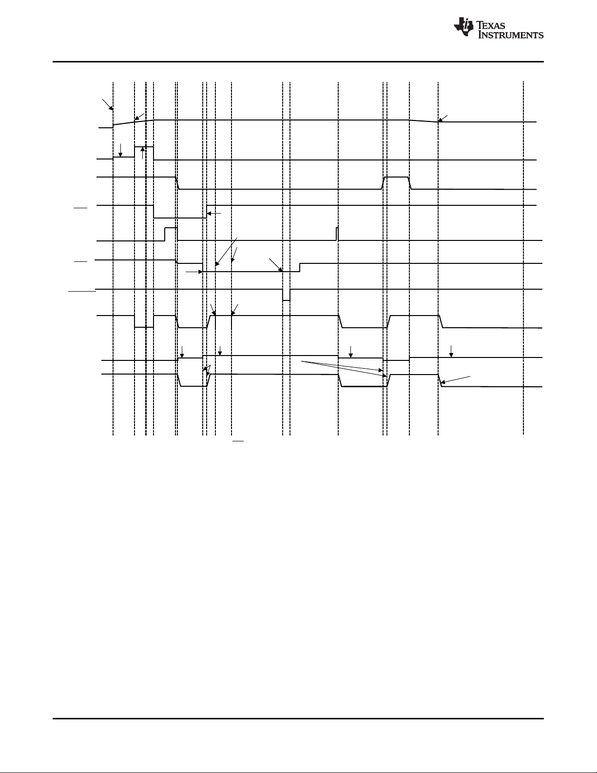
VIN
SW
SYS
VBAT
CD
PG
IBAT
PMID
Insert
Battery
Apply
VIN
VIN > UVLO
After delay of several ms,
switching starts and SYS
starts to rise
Charging
enabled
Charging
disabled
VBAT
rises
VBAT = V
BATREG
Charge
Current
Taper
IBAT=ICHRG
VBAT =
V
BATREG
- V
RCHG
IBAT = I
TERM
BAT supplies SYS
when VIN removed
INT
BAT IQ
Typical Start-Up Timing and Operation
VBAT>V
BUVLO
Remove
Battery
Shows
Charge
Status
VISET
<3uA max <4uA max
No SYS Load
SYS Load Applied
<3uA max
<5uA max
<4uA max
nA of leakage with VIN present
0mA
www.ti.com
bq25120A
SLUSD08A –MAY 2017–REVISED JANUARY 2018
Conditions: PGB_MRS = 0, TE = 1, SW_LDO = 1, VINDPM_ON = 0, PG and INT pulled up to SYS, EN_INT = 1
Figure 1. Typical Start-Up Timing and Operation
Product Folder Links: bq25120A
Submit Documentation FeedbackCopyright © 2017–2018, Texas Instruments Incorporated
13
SYS
VBAT
CD
Insert Battery <
V
BATSHORT
INT
BAT IQ
IBAT
VBAT=V
BUVLO
IBAT = I
BATSHORT
VIN
IBAT = ICHG
MR
<1uA max
RESET
MR_WAKE1
Interrupt
MR_WAKE2
Interrupt
<3uA max
MR_WAKE1 time reached
MR_WAKE2 time reached
MRRESET time reached
t
RESET
After delay of several ms,
SYS starts to rise
Device enters Active Battery
Mode after valid /MR
<1uA max
User depresses button
SYS is pulled down shortly
after VBATUVLO is reached
VBAT=V
BUVLO
<3uA max
bq25120A
SLUSD08A –MAY 2017–REVISED JANUARY 2018
www.ti.com
14
Conditions: SW_LDO = 1, MRREC = 1, PG and INT pulled up to SYS, ISYS = 10 µA, EN_INT = 1
Figure 2. Battery Operation and Sleep Mode
Submit Documentation Feedback Copyright © 2017–2018, Texas Instruments Incorporated
Product Folder Links: bq25120A
Temperature (qC)
R
DS(ON)
(m:)
-40 -25 -10 5 20 35 50 65 80 95 110 125
0
50
100
150
200
250
300
350
400
D025
Temperature (qC)
Accuracy
-40 -10 20 50 80 110 125
-0.5%
-0.3%
-0.1%
0.1%
0.3%
0.5%
D019
4.35 V
(BATREG)
4.2 V
(BATREG)
4 V
(BATREG)
3.8 V
(BATREG)
3.6 V
(BATREG)
BAT (V)
BAT I
Q
(PA)
3 3.2 3.4 3.6 3.8 4 4.2 4.4 4.6
0.00
0.02
0.04
0.06
0.08
0.10
0.12
0.14
D018
85qC
60qC
25qC
0qC
Temperature (qC)
R
DS(ON)
(m:)
-40 -25 -10 5 20 35 50 65 80 95 110 125
0
100
200
300
400
500
600
700
D024
BAT (V)
BAT I
Q
(PA)
3 3.2 3.4 3.6 3.8 4 4.2 4.4 4.6
0
2
4
6
8
10
12
D016
85qC
60qC
25qC
0qC
BAT (V)
BAT I
Q
(PA)
3 3.2 3.4 3.6 3.8 4 4.2 4.4 4.6
0.0
0.5
1.0
1.5
2.0
D017
85qC
60qC
25qC
0qC
www.ti.com
8.7 Typical Characteristics
bq25120A
SLUSD08A –MAY 2017–REVISED JANUARY 2018
1.8 V System Enabled (No Load)
Figure 3. Active BAT, I
Figure 5. Ship Mode BAT, I
Q
Q
Figure 6. Blocking FET R
Figure 4. Hi-Z BAT, I
DS(ON)
Q
vs Temperature
Figure 7. Battery Discharge FET R
vs Temperature Figure 8. V
DS(ON)
Product Folder Links: bq25120A
(BATREG)
Submit Documentation FeedbackCopyright © 2017–2018, Texas Instruments Incorporated
Accuracy vs Temperature
15
Temperature (qC)
R
DS(ON)
(m:)
-40 -25 -10 5 20 35 50 65 80 95 110 125
0
50
100
150
200
250
300
350
400
D027
Frequency (Hz)
PSRR (dB)
10 20 50 100 1000 10000 100000 1000000
0
20
40
60
80
100
120
140
160
D028
Noise Floor
1 mA
10 mA
50 mA
100 mA
Pre-Charge Current (mA)
Accuracy
0 5 10 15 20 25 30 35 40
-10%
-8%
-6%
-4%
-2%
0
2%
4%
6%
8%
10%
D022
-40qC
0qC
25qC
85qC
125qC
Temperature (qC)
R
DS(ON)
(m:)
-40 -25 -10 5 20 35 50 65 80 95 110 125
0
100
200
300
400
500
600
700
800
900
1000
D026D024
Input Current Limit (A)
Accuracy
0.05 0.1 0.15 0.2 0.25 0.3 0.35 0.4
-5%
-4%
-3%
-2%
-1%
0
1%
2%
3%
4%
5%
D020
-40qC
0qC
25qC
85qC
125qC
Charge Current (mA)
Accuracy
0 50 100 150 200 250 300
-5%
-3%
-1%
1%
3%
5%
D021
-40qC
0qC
25qC
85qC
125qC
bq25120A
SLUSD08A –MAY 2017–REVISED JANUARY 2018
Typical Characteristics (continued)
Figure 9. ILIM Accuracy vs Input Current Figure 10. Charge Current Accuracy vs Charge Current
www.ti.com
Figure 11. Pre-Charge Accuracy vs Pre-Charge Current
16
VIN= 5 V
Figure 13. R
of Low Side MOSFET vs Temperature Figure 14. LS/LDO PSRR vs Frequency
DS(ON)
Submit Documentation Feedback Copyright © 2017–2018, Texas Instruments Incorporated
VIN= 5 V
Figure 12. R
Product Folder Links: bq25120A
of High Side MOSFET vs Temperature
DS(ON)
SW
MR
TS
LS/LDO
BAT
PWM, LDO, and BAT FET
Control
I2C
Interface
Hi-Z
Mode
Device Control
Reset and
Timer
+
+
+
+
VIN
TS COLD
TS HOT
TS WARM
TS COOL
SYS
1C/
0.5C
Disable
Disable
VBATREG
± 140mV
LDO/ Load Switch
Control
I
INLIM
Q1/Q2
Q3
Q4
V
IN_DPM
V
SUPPLY
V
BATREG
LDO
Control
V
SYSREG
Thermal
Shutdown
+
+
Termination
Reference
I
BAT
V
IN
V
INOVP
V
BAT
V
BATOVP
V
BATREG
± 0.12 V
V
BAT
V
BAT
V
BATSHRT
I
BATREG
+
+
+
RESET
Q5
Q7
VOVP
BATOVP
BATSHRT
Recharge
PMID
LDO/ Load Switch
Host Control
Input Current Limit
Charge Current
Termination Current
PG
+
V
BAT(SC)
SDA
SCL
LSCTRL
ILIM
ISET
INT
GND
IN
VINLS
CD
Copyright © 2016, Texas Instruments Incorporated
S
D
G
S
D
G
S
D
G
bq25120A
www.ti.com
SLUSD08A –MAY 2017–REVISED JANUARY 2018
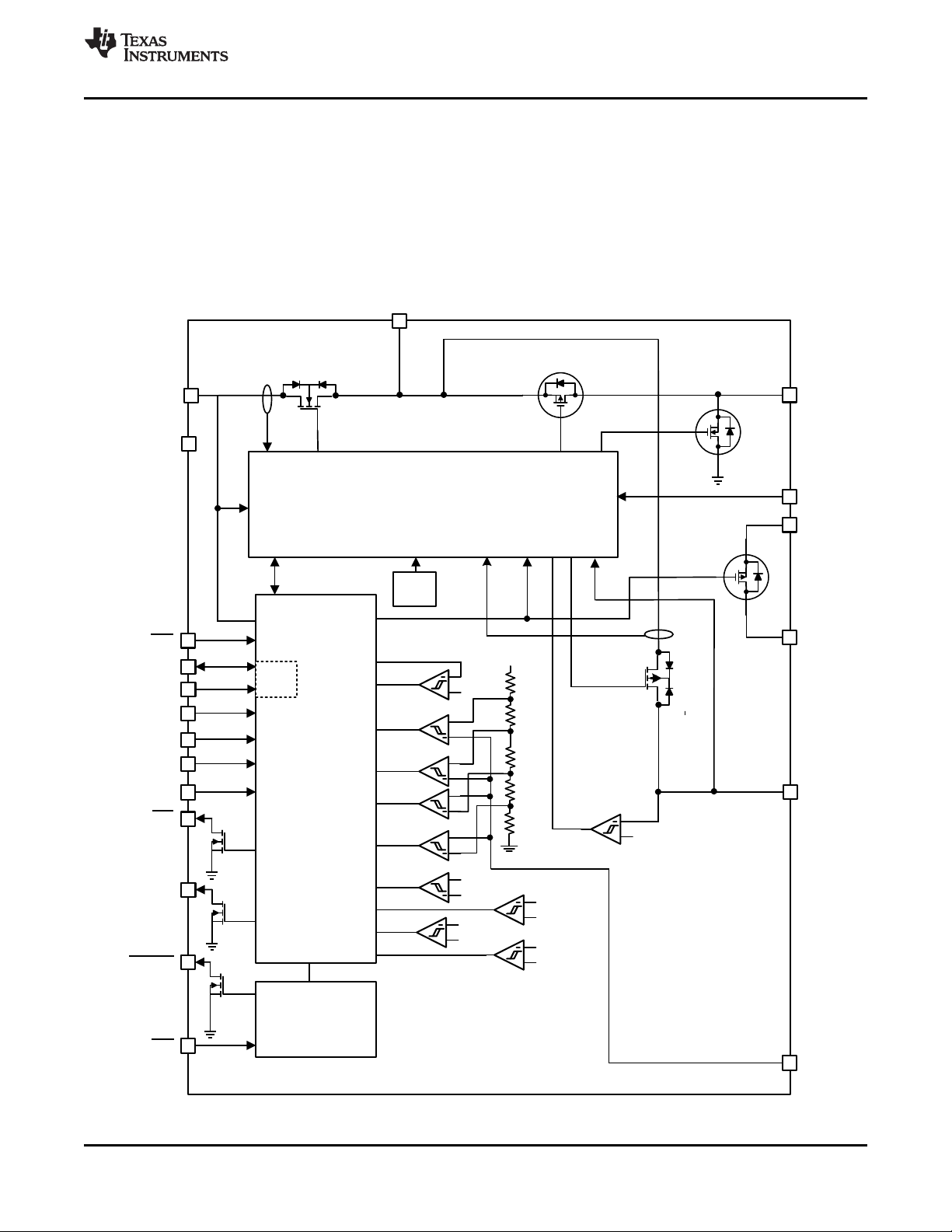
9 Detailed Description
9.1 Overview
The following sections describe in detail the functions provided by the BQ25120A. These include linear charger,
PWM output, configurable LS/LDO output, Push-button input, reset timer, functional modes, battery monitor, I2C
configurability and functions, and safety features.
9.2 Functional Block Diagram
Product Folder Links: bq25120A
Submit Documentation FeedbackCopyright © 2017–2018, Texas Instruments Incorporated
17
VIN
MR
CD
I2C
Write
t
QUIET
bq25120A
SLUSD08A –MAY 2017–REVISED JANUARY 2018
www.ti.com
9.3 Feature Description
9.3.1 Ship Mode
Ship Mode is the lowest quiescent current state for the device. Ship Mode latches off the device and BAT FET
until VIN> V
that are active during Ship Mode:
1. VIN_UV Comparator
2. MR Input (No clock or delay in this mode for lowest power consumption)
3. PMID active pull down
9.3.1.1 Ship Mode Entry and Exit
The device may only enter Ship Mode when there is not a valid VIN supply present (VIN< V
supply is removed there are two ways for the device to enter Ship Mode: through I2C command using the
EN_SHIPMODE bit and by doing a long button press when MRREC bit is set to 0. If the EN_SHIPMODE bit is
set while the IN supply is present, the device will enter Ship Mode upon removal of the supply. The
EN_SHIPMODE bit can be cleared using the I2C interface as well while the IN input is valid.
In addition to VIN< V
the transition to Ship Mode. All three conditions must remain unchanged for a period of t
operation. Figure 15 and Figure 16show the correct sequencing to ensure proper entry into the Ship Mode
through I2C command and MR button press respectively.
BAT
+ V
or the MR button is depressed for t
SLP
, CD and MR must be high. Once all of these conditions are met the device will begin
UVLO
and released. The following list shows the events
WAKE1
UVLO
to ensure proper
QUIET
). Once the IN
18
Figure 15. CD, MR and VIN Sequencing for Ship Mode Entry Through I2C Command
Submit Documentation Feedback Copyright © 2017–2018, Texas Instruments Incorporated
Product Folder Links: bq25120A
VIN
MR
CD
I2C
Write
t > t
RESET
t
QUIET
www.ti.com
Feature Description (continued)
Figure 16. CD, MR and VIN Sequencing for Ship Mode Entry Through Long MR button press
bq25120A
SLUSD08A –MAY 2017–REVISED JANUARY 2018
The end user can enable the device (exit Ship Mode) by connecting an adapter to IN (VIN> V
BAT
+ V
SLP
) or by
toggling the MR button. Note that in the case where an adapter is connected while the MR is still held low and
immediately after the RESET timer has expired (MR low for t
), the device will not enter Ship Mode, but may
RESET
enter it upon adapter removal (Same behavior as setting the EN_SHIPMODE bit when the adapter is present).
This will not be the case if MR has gone high when the adapter is connected or MR continues to be held low for
a period longer than t
after the adapter is connected.
WAKE1
To exit Ship Mode through and MR press the battery voltage must be above the maximum programmable
BUVLO threshold when VINis not present. Once MR goes low, the device will start to exit Ship Mode, powering
PMID. The device will not complete the transition from Ship Mode until MR has been held low for at least t
WAKE1
Only after the transition is complete may the host start I2C communication if the device has not entered High
Impedance Mode.
9.3.2 High Impedance Mode
High Impedance mode is the lowest quiescent current state while operating from the battery. During Hi-Z mode
the SYS output is powered by BAT, the MR input is active, and the LSCTRL input is active. All other circuits are
in a low power or sleep state. The LS/LDO output can be enabled in Hi-Z mode with the LSCTRL input. If the
LS/LDO output has been enabled through I2C prior to entering Hi-Z mode, it will stay enabled. The CD pin is
used to put the device in a high-impedance mode when battery is present and VIN< V
. Drive CD high to
UVLO
enable the device and enter active battery operation when VINis not valid. When the HZ_MODE bit is written by
the host, the I2C interface is disabled if only battery is present. To resume I2C, the CD pin must be toggled. If the
supply for the CD pull up glitches or experiences a brownout condition , it is recommended to toggle the /CD pin
to resume I2C communication.. The functionality of the pin is shown in Table 1.
Table 1. CD, State Table
CD, State VIN< V
L Hi-Z Charge Enabled
H Active Battery Charge Disabled
UVLO
VIN> V
UVLO
.
Product Folder Links: bq25120A
Submit Documentation FeedbackCopyright © 2017–2018, Texas Instruments Incorporated
19
bq25120A
SLUSD08A –MAY 2017–REVISED JANUARY 2018
www.ti.com
9.3.3 Active Battery Only Connected
When the battery above V
BATUVLO
After the battery rises above V
is connected with no input source, the battery discharge FET is turned on.
BATUVLO
and the deglitch time is reached, the SYS output starts to rise. The current
from PMID and SYS is not regulated, but is protected by a short circuit current limit. If the short circuit limit is
reached for the deglitch time (t
), the battery discharge FET is turned off for the recovery time (t
DGL_SC
REC_SC
After the recovery time, the battery FET is turned on to test if the short has been removed. If it has not, the FET
turns off and the process repeats until the short is removed. This process protects the internal FET from over
current. During this event PMID will likely droop and cause SYS to go out of regulation.
To provide designers the most flexibility in optimizing their system, an adjustable BATUVLO is provided. When
the voltage drops below the V
BATUVLO
threshold, the battery discharge FET is turned off. Deeper discharge of the
battery enables longer times between charging, but may shorten the battery life. The BATUVLO is adjustable
with a fixed 150-mV hysteresis.
).
If a valid VINis connected during active battery mode, VIN> V
turned on when the battery voltage is above the minimum V
BATUVLO
Drive CD high or write the CE register to disable charge when VIN> V
, the supplement and battery discharge FET is
UVLO
.
is present. CD is internally pulled
UVLO
down. When exiting this mode, charging resumes if VINis present, CD is low and charging is enabled.
All HOST interfaces (CD, SDA/SCL, INT, RESET and LSCTRL) are active no later than 5 ms after SYS reaches
the programmed level.
9.3.4 Voltage Based Battery Monitor
The device implements a simple voltage battery monitor which can be used to determine the depth of discharge.
Prior to entering High-Z mode, the device will initiate a VBMON reading. The host can read the latched value for
the no-load battery voltage, or initiate a reading using VBMON_READ to see the battery voltage under a known
load. The register will be updated and can be read 2ms after a read is initiated. The VBMON voltage threshold is
readable with 2% increments with ±1.5% accuracy between 60% and 100% of VBATREG using the VBMON_TH
registers. Reading the value during charge is possible, but for the most accurate battery voltage indication, it is
recommended to disable charge, initiate a read, and then re-enable charge.
A typical discharge profile for a Li-Ion battery is shown in Table 2. The specific battery to be used in the
application should be fully characterized to determine the thresholds that will indicate the appropriate battery
status to the user. Two typical examples are shown below, assuming the VBMON reading is taken with no load
on the battery.
This function enables a simple 5-bar status indicator with the following typical performance with different
VBATREG settings:
Table 2. Discharge Profile for a Li-Ion Battery
VBATREG BATTERY FULL
4.35 V VBMON > 90% VBMON = 88% VBMON = 86% VBMON = 84% VBMON < 82%
4.2 V VBMON > 98% VBMON = 94% or 96% VBMON = 90% or 92% VBMON = 86% or 88% VBMON < 84%
95% to 65%
REMAINING CAPACITY
65% to 35%
REMAINING CAPACITY
35% to 5%
REMAINING CAPACITY
BATTERY EMPTY
20
Submit Documentation Feedback Copyright © 2017–2018, Texas Instruments Incorporated
Product Folder Links: bq25120A
D
E
C
O
D
E
R
S 3
S 2
S 1
S 0
- 2 % BAT TAP
- 4 % BAT TAP
- 6 % BAT TAP
- 8 % BAT TAP
- 10 % BAT TAP
VREF
90 % VB
80 % VB
70 % VB
60 % VB
VB = 0 . 8 VBAT
VBGUAGE_TH<2:0>
www.ti.com
bq25120A
SLUSD08A –MAY 2017–REVISED JANUARY 2018
Figure 17. Voltage Battery Monitor
9.3.5 Sleep Mode
The device enters the low-power sleep mode if the voltage IN falls below the sleep-mode entry threshold and V
is higher than the undervoltage lockout threshold. In sleep mode, the input is isolated from the connected battery.
This feature prevents draining the battery during the absence of VIN. When VIN< V
the battery discharge FET on, sends a 128-µs pulse on the INT output, and the FAULT bits of the register are
update over I2C. Once VIN> V
cleared until they are read over I2C and the sleep condition no longer exists. It is not recommended to do a
battery connection or plug in when V
drained form the battery.
9.3.6 Input Voltage Based Dynamic Power Management (V
(BAT)
+ V
, the device initiates a new charge cycle. The FAULT bits are not
SLP
< VIN < V
UVLO
BAT
+ V
as it may cause higher quiescent current to be
SLP
)
IN(DPM)
(BAT)
+ V
, the device turns
SLP
During the normal charging process, if the input power source is not able to support the programmed or default
charging current and System load, the supply voltage decreases. Once the supply approaches V
DPM current and voltage loops will reduce the input current through the blocking FETs, to prevent the further
drop of the supply. The V
IN(DPM)
threshold is programmable through the I2C register from 4.2 V to 4.9 V in 100mV steps. It can be disabled completely as well. When the device enters this mode, the charge current may be
lower than the set value and the VINDPM_STAT bit is set. If the 2X timer is set, the safety timer is extended
while V
IN(DPM)
connected while V
is active. Additionally, termination is disabled. Note that in a condition where the battery is
UVLO<VIN
< V
, the VINDPM loop will prevent the battery from being charged and PMID
IN(DPM)
will be powered from BAT.
IN(DPM)
, the input
IN
Product Folder Links: bq25120A
Submit Documentation FeedbackCopyright © 2017–2018, Texas Instruments Incorporated
21

bq25120A
SLUSD08A –MAY 2017–REVISED JANUARY 2018
www.ti.com
9.3.7 Input Overvoltage Protection and Undervoltage Status Indication
The input overvoltage protection protects the device and downstream components connected to PMID, SYS, and
BAT against damage from overvoltage on the input supply. When VIN> V
an OVP fault is determined to exist.
OVP
During the OVP fault, the device turns the battery discharge FET on, sends a single 128-µs pulse on INT, and
the FAULT bits are updated over I2C. Once the OVP fault is removed, after the deglitch time, t
DGL_OVP
, STAT and
FAULT bits are cleared and the device returns to normal operation. The FAULT bits are not cleared until they are
read in from I2C after the OVP condition no longer exists. The OVP threshold for the device is set to operate from
standard USB sources.
The input under-voltage status indication is used to notify the host or other device when the input voltage falls
below a desired threshold. When VIN< V
, after the deglitch time t
UVLO
DGL_UVLO
, a UVLO fault is determined to
exist. During the VINUVLO fault, the device sends a single 128-µs pulse on INT, and the STAT and FAULT bits
are updated over I2C. The FAULT bits are not cleared until they are read in from I2C after the UVLO condition no
longer exists.
9.3.8 Battery Charging Process and Charge Profile
When a valid input source is connected (VIN> V
UVLO
and V
(BAT)
+ V
< VIN< V
SLP
and VIN> V
OVP
IN(DPM)
), the CE
bit in the control register determines whether a charge cycle is initiated. When the CE bit is 1 and a valid input
source is connected, the battery discharge FET is turned off, and the output at SYS is regulated depending on
the output configuration. A charge cycle is initiated when the CE bit is written to a 0. Alternatively, the CD input
can be used to enable and disable charge.
The device supports multiple battery chemistries for single-cell applications. Charging is done through the
internal battery MOSFET. There are several loops that influence the charge current: constant current loop (CC),
constant voltage loop (CV), input current limit, V
DPPM
, and V
. During the charging process, all loops are
IN(DPM)
enabled and the one that is dominant takes control.
The charge current is regulated to I
CHARGE
voltage. The voltage between BAT and GND is regulated to V
until the voltage between BAT and GND reaches the regulation
BATREG
(CV Mode) while the charge current
naturally tapers down. When termination is enabled, the device monitors the charging current during the CV
mode, and once the charge current tapers down to the termination threshold, I
, and the battery voltage is
TERM
above the recharge threshold, the device terminates charge, and turns off the battery charging FET. Termination
is disabled when any loop is active other than CV.
9.3.9 Dynamic Power Path Management Mode
With a valid input source connected, the power-path management circuitry monitors the input voltage and current
continuously. The current into IN is shared at PMID between charging the battery and powering the system load
at PMID, SYS, and LS/LDO. If the sum of the charging and load currents exceeds the current that the VIN can
support, the input DPM loop(VINDPM) reduces the current going into PMID through the input blocking FETs.
This will cause a drop on the PMID voltage if the system demands more current. If PMID drops below the DPPM
voltage threshold(V
), the charging current is reduced by the DPPM loop through the BATFET in order to
DPPM
stabilize PMID. If PMID continues to drop after BATFET charging current is reduced to zero, the part enters
supplement mode when PMID falls below the supplement mode threshold. Battery termination is disabled while
in DPPM mode. In order to charge the battery, the voltage at PMID has to be greater than V
BATREG
+ V
DPPM
threshold..
9.3.10 Battery Supplement Mode
While in DPPM mode, if the charging current falls to zero and the system load current increases beyond the
programmed input current limit, the voltage at PMID reduces further. When the PMID voltage drops below the
battery voltage by V
system load when the voltage on the PMID pin rises above the battery voltage by V
, the battery supplements the system load. The battery stops supplementing the
(BSUP1)
. During supplement
(BSUP2)
mode, the battery supplement current is not regulated, however, the short-circuit protection circuit is active.
Battery termination is disabled while in supplement mode.
22
Submit Documentation Feedback Copyright © 2017–2018, Texas Instruments Incorporated
Product Folder Links: bq25120A
 Loading...