

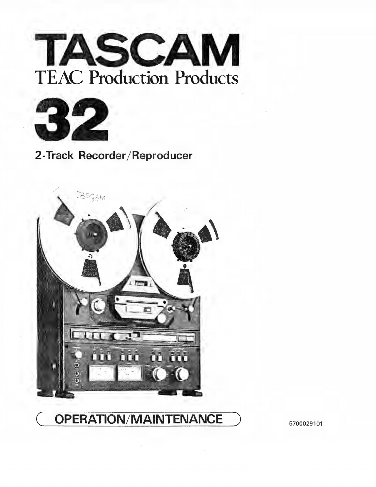
Tascam 32 Operation Manual
M
TEAC Production Products
2-Track Recorder /
Reproducer
( OPERATION/MAINTENANCE )
5700029101
MAINTENANCE
Note:
Parts reference numbers used
description may not always correspond
of
the
Model
sections:
and
REW
System, 1-13
Amplifier Circuit Description.
32,
except
1-5
Reel Motor Drive Circuit, 1-9 F.F
Operation, 1-10 Electrical Brake
Ed
it Control Circu it and 1-16
for
in
the
the
circuit
to
those
following
NOTES
* All resistors are 1
otherwise. Resistor values are
ohms, M=1,000,000 ohms).
* All capacitor values are
farads).
/4
watts, 5
%,
unless marked
in
ohms (K=1,000-
in
microfarads (p=pico-
* & Parts marked with this sign are safety critical
components. They must always
with indentical
Parts List and ensure exact replacement.
* 0 dB
*
is
referenced
otherwise specified.
PC
boards shown viewed from foil side.
components-
to
1 V
in
be
replaced
refer
to
the TEAC
this manual unless
Effective:
Januar1.
1982
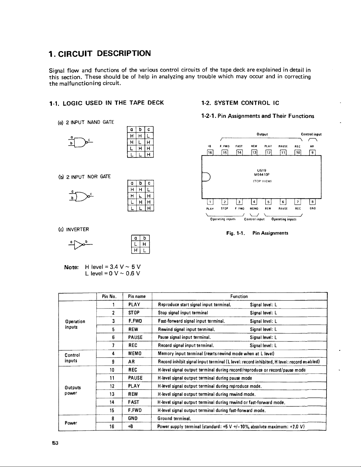
1.
CIRCUIT
DESCRIPTION
Signal
flow
and functions
this section. These should
the
malfunctioning
1-1.
LOGIC
(a)
2
INPUT
(b)
2
INPUT
(c)
INVERTER
USED
NAND
NOR
circuit.
IN
THE TAPE DECK
GATE
GATE
of
the various control circuits
be
of help in analyzing any trouble which may occur
of
the tape deck
1-2. SYSTEM CONTROL IC
1-2-1.
Pin
Assignments
a b
C
H
H
L
H L
L H
L L
0 b
H H
H
L
L L
b.
H
H
H
H
C
L
H
H
H
•B
f,
FWO
FAST
2
3
PLAY
STOP f FWO
Operating ,nputs Contra! input Operating inputs
Fig. 1-1. Pin Assignments
are
explained in detail in
and
in correcting
and
Their Functions
Output Control input
REW
PLAY
PAUSE
REC
U519
M54410P
!TOP
VIEWI
4
5 6
MEMO
REW
PAUSE
REC
/\
AR
GNO
Note: H level = 3.4 V ~ 5 V
L level = 0
Operation
inputs
Control
inputs
Outputs
power
Power
Pin
No.
1
2
3
5
6
1
4
9
10
11
12
13
14
15
8
16
V~
0.6 V
Pin
name
PLAY
STOP
F.FWD
REW
PAUSE
REC
MEMO
AR
REC
PAUSE
PLAY
REW
FAST
F.FWD
GNO
+B
Reproduce
Stop
signal
Fast-forward
Rewind
signal
Pause
signal
Record
signal
Memory
input
Record
inhibit
H-level
signal
H•level
signal
H-level
signal
H-level
signal
H-level
signal
H-level
signal
Ground
terminal.
Power
supply
start
input
signal
input
input
input
terminal
signal
output
output
output
output
output
output
terminal
signal
terminal
input
terminal.
terminal.
terminal.
input
terminal
terminal
terminal
terminal
terminal
terminal
input
terminal.
terminal.
(resets
rewind
terminal
during
during
during
during
during
during
(standard:
Function
mode
when
( L
level:
record
record/reproduce
pause
mode
reproduce
rewind
mode.
rewind
or
fast-forward
+5
V
+/-10%,
Signal
level:
Signal
level:
Signallevel:
Signal
level:
Signallevel:
Signal
level:
at L
level)
inhibited, H level:
or
record/pause
mode.
fast-forward
mode.
absolute
maximum:
L
L
L
L
L
L
mode.
record
mode
+7.0
V)
e~
abled)
53
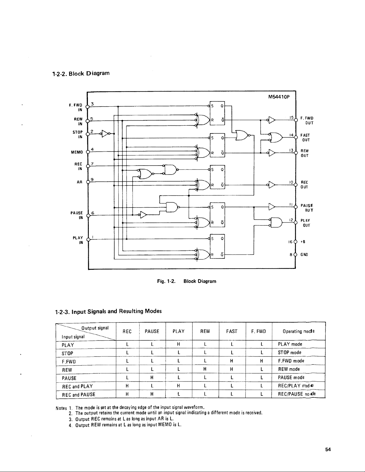
1-2-2. Block Diagram
FWD
IN
REW
IN
IN
REC
IN
AR
3
5
4
7
9
6
IN
F.
STOP
MEMO
PAUSE
M54410P
10
F.
FWD
OUT
FAST
OUT
REW
OUT
REC
OUT
PAUSE
OUT
PUY
OUT
PLAY
IN
Fig.
1-2-3. Input Signalsand Resulting Modes
0
utp
ut
1
nput
PLAY
STOP
F.FWD
REW
PAUSE
REC
REC
Notes
signal
and
PLAY
and
PAUSE
1.
The
mode
2.
The
output
3.
Output R EC
4.
Output
signal
is
REW
set
at
retains
remains
remains
the
the
at
at
REC
decaying
current
Las
L
L L
L
L L
L
H L
H
Las
mode
long
long
edge
as
as
PAUSE
L
L
H
H
of
the
until
input
input
AR
1-2.
input
an
input
is
MEMO
Block
Diagram
PLAY
H L
REW
L L
L L
L
H
L L
H L
l L L
signal
waveform.
signal
indicating a different
L.
is
L.
FAST
F.
L
L L
H
H L
L
L L
mode
is
received.
FWD
L
H
L
L
+B
16
GND
8
Operating
PLAY
mode
STOP
mode
F.FWD
mode
REW
mode
PAUSE
mode
REC/PLAY
REC/PAUSE
riode
mode
mocle
54
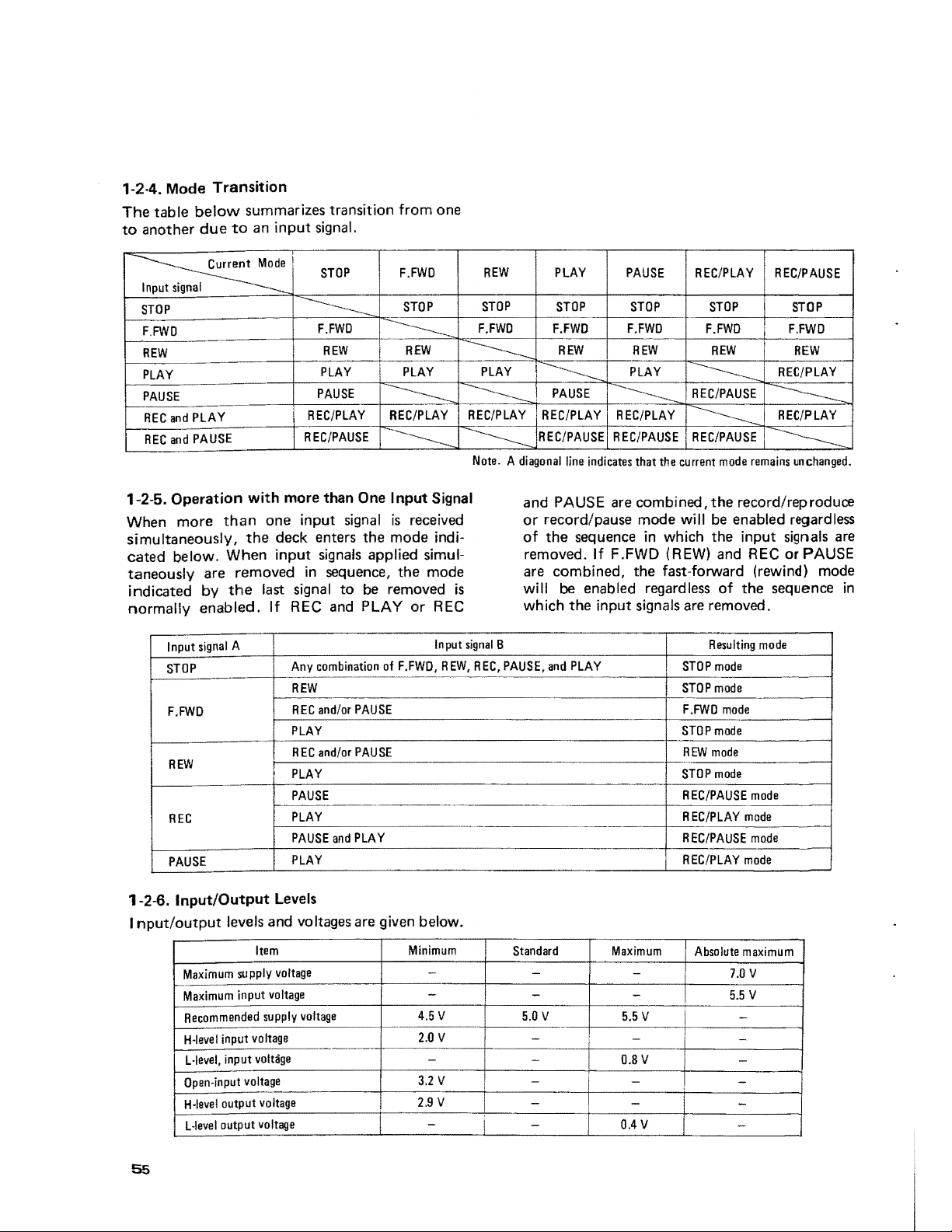
1-2-4. Mode Transition
The
table
to
another
below
due
summarizes
to
an
input
transition
signal.
from
one
Gurrent
1
nput
signal
STOP
F.FWD
REW
PLAY
PAUSE
REG
and
PLAY
REG
and
PAUSE
1-2-5. Operation with more than
When
simultaneously,
cated
taneously
indicated
normally
more
below.
Input
STOP
F.FWD
REW
REC
PAUSE
are
by
enabled.
signal
than
the
When
removed
the
A
Mode
one
last signal
lf REC and
STOP
F.FWD
-----
REW
PLAY
PAUSE
REG/PLAY
REC/PAUSE
input
deck
enters
input
signals
in
Any
combination
REW
REC
and/or
PLAY
R
EC
and/or
PLAY
PAUSE
PLAY
PAUSE
PLAY
signal
sequence,
to
and
F.FWD
STOP
REW
-------
PLAY
REC/PLAY
-----
-----
One
Input
is
received
the
mode
applied
the
be removed
PLAY
PAUSE
PAUSE
PLA
of
Y
or
F.FWD,
-----
~
REC/PLAY
----------
Signal
indi-
simul-
mode
is
REC
Input
signal
REW,
REW
STOP
F.FWD
PLAY
Note. A diagonal
B
REC,
PAUSE,
F.FWO
PAUSE
-----
REC/PLAY
REC/PAUSE
and
or
record/pause
of
the
removed.
are
combined,
will be
which
and
PLAY
STOP
REW REW
line
PAUSE
sequence
the
PLAY
PAUSE
STOP
F.FWD
PLAY
REC/PLAY
-------
REC/PAUSE
indicates
enabled
that
are
combined,
mode
in which
lf F.FWD (REW)
the
input
signals
REG/PLAY
STOP
F.FWO
REW
REC/PAUSE
----------
~
REC/PAUSE
the
current
mode
the
will be
the
and
fast-forward (rewind) mode
regardless
of
are
removed.
Resulting
STOP
mode
STOP
mode
F.FWD
mode
STOP
mode
REW
mode
STOP
mode
R
EC/PAUSE
REG/PLAY
REG/PAUSE
R
EC/PLA Y mode
REG/PAUSE
STOP
F.FWO
REW
REC/PLAY
REC/PLAY
-----
remains
unchanged.
-----
record/reproduce
enabled
input
the
REC
mode
mode
mode
mode
regardless
signals are
or
PAUSE
sequence
in
1-2-6.
Input/Output
1
nput/output
Maximum
Maximum
Recommended
H•level
L-level,
Open-input
H-level
L-level
55
levels
supply
input
input
input
voltage
output
output
Levels
and
ltem
voltage
voltage
supply
voltage
voltage
voltage
voltage
voltages
voltage
are
given below.
Minimum
-
4.5
V
2.0
V -
3.2
V -
2.9
V
1
Standard
-
-
5.0
V
-
- -
-
Maximum
5.5
V
-
0.8V
0.4
V
Absolute
7.0
5.5
maximum
V
V
-
-
-
-
-
-
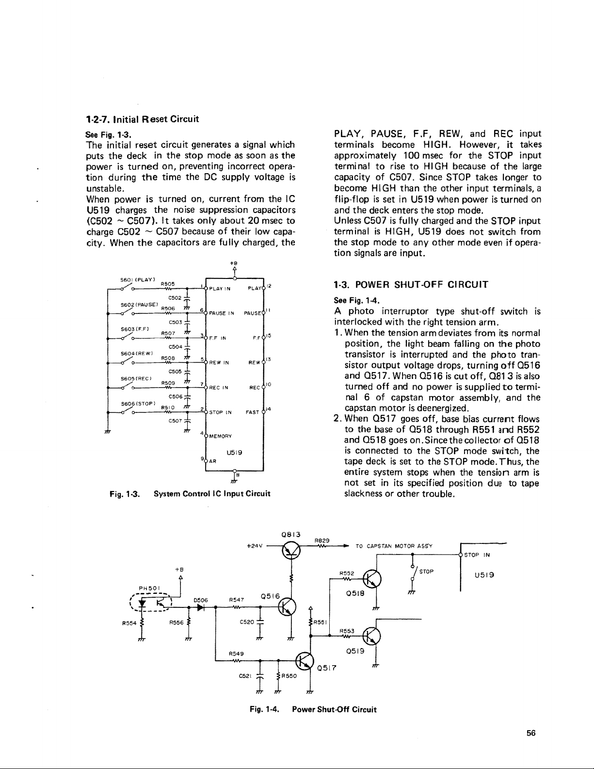
1-2-7.
Initial
Reset
Circuit
See Fig. 1-3.
The initial
puts
power
tion during
the
is
reset
deck
turned
the
circuit generates a signal which
in
the
stop mode as soon as
on,
preventing incorrect opera-
time
the
DC
unstable.
When power is turned on,
U519 charges
(C502 ~
C507).
the
no
lt
takes only
ise
suppression capacitors
charge C502 ~ C507 because
city. When
fig.
the
5601
(PLAY)
$602
(PAUSE)
5603
(F.F)
S604(REW)
5605
(REC
5606(STOPI
1-3.
capacitors are fully charged,
R505
C502
l
R506
C503
R507
C504
R508
C505
1
R509
C506l
R510
C507
System Control
6
l-
l
l
7
2
l
4
9
supply voltage
current
PLAY
PAUSE IN PAUSE
F.F
REW
REC
STOP
MEMORY
AR
lC
from
about
20
of
their low capa-
+B
PLAY
lN
IN
U519
F.F
REW
REC
FAST
8
IN
IN
IN
Input Circuit
the
msec
12
II
15
13
10
14
the
is
IC
to
the
PLAY, PAUSE,
F.F,
REW,
and REC input
terminals become HIGH. However, it takes
approximately 100 msec
terminal
capacity
becorne
flip-flop
and
Unless C507
terminal
the
to
rise
to
of
C507. Since STOP takes langer
HIGH
than
is
set
in
U519 when power
the
deck enters the stop mode.
is
fully charged
is
HIGH, U519 does
stop
mode
to
any
for
the
STOP input
HIGH
because of
the
other input terminals, a
isturned
and
the
STOP input
not
switch from
other
mode even if opera-
the
large
to
an
tion signals are input.
1-3.
POWER SHUT-OFF CIRCUIT
See Fig. 1-4.
A
photo
interlocked with
1. When
position,
transistor
sistor
and
turned
nal 6 of
capstan
2. When
to
and
is
tape
entire system stops when the tension arm
not
slackness or
interruptor type shut-off switch
the
right tension arm.
the
tension arm deviates from its normal
the
light beam falling on
is
interrupted and
output
0517.
voltage drops, turning
When
0516
off
and no power
is
cut
is
supplied
capstan motor assembly,
motor
0517
the
base
0518
connected
deck
set
is
deenergized.
goes off, base bias
of
0518
through R551 and R552
goes
on.Sincethecollector
to
the STOP mode switch,
is
set
to
the STOP mode. Thus,
in
its specified position due to tape
other
trouble.
the
the
photo
off
off, 081 3
to
and
current
of
photo
tran-
0516
is
also
termi-
the
flows
0518
the
the
is
is
Fig.
1-4. Power Shut-Off Circuit
TO
CAPSTAN
,-----+-----OSTOP
MOTOR
lSTOP
ASS'Y
IN
U519
56
3.
When
the
tension arm
the
photo
and
outputs
and
0517
4.
When
Q516goeson,
is
grounded and
capstan
5.
When
turned
motor.
0517
off,
mode switch and
circuit.
is
in its normal position,
transistor
a high ievel voltage
receives
conduct.
the
0813
0813
supplies current
goes
on,
0518
disconnecting
0519
from the
base
0518
the light
to
make
bias
and
0519
from
the stop
speed
beam
0516
circuit
to
the
are
sensing
the
activation force
but
minimizing heating
holding.
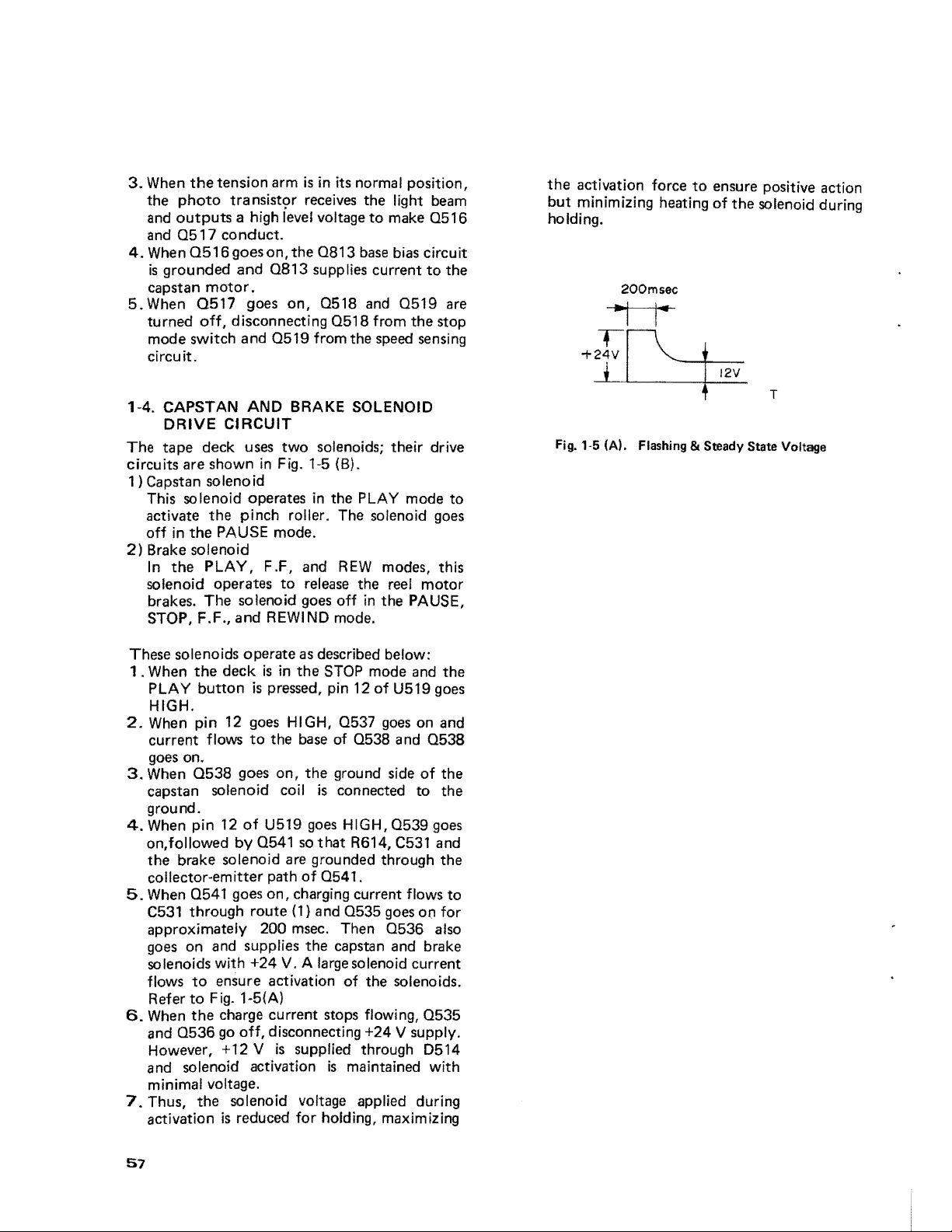
200msec
to
ensure positive action
of
the solenoid during
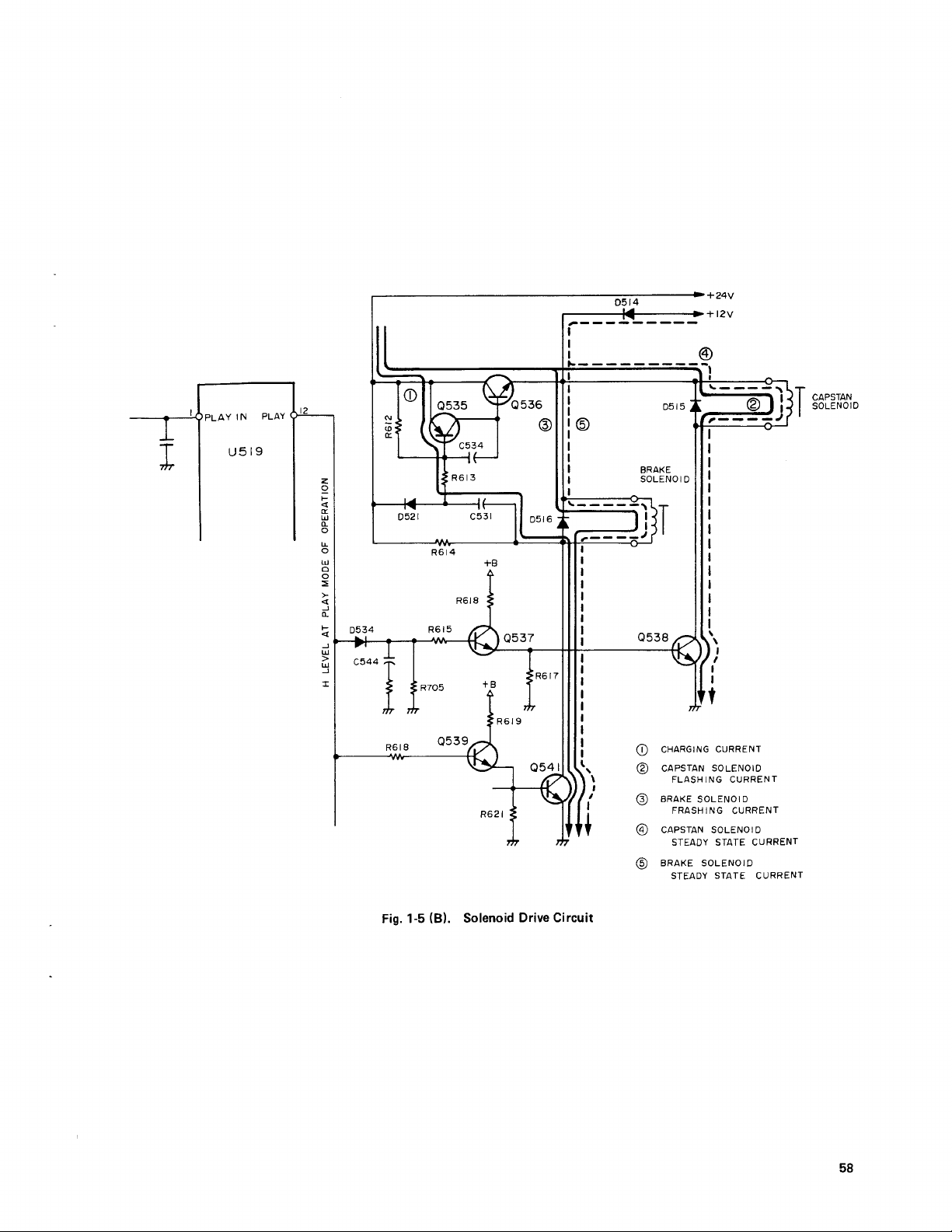
1-4. CAPSTAN
DRIVE
The tape deck
circuits are shown
1)
Capstan solenoid
AND
CIRCUIT
uses
two
in
Fig. 1-5 (B).
BRAKE SOLENOID
solenoids; their drive
This solenoid operates in the PLAY mode
activate the pinch roller. The solenoid
off
in the PAUSE mode.
2)
Brake solenoid
In
the
PLAY,
solenoid operates
brakes. The solenoid
F.F, and
to
release
goes
REW
modes, this
the
reel
off
in the PAUSE,
STOP, F.F., and REWIND mode.
These solenoids operate
1 . When
PLAY
the
deck
button
is
as
described below:
is
in the
STOP
pressed, pin
mode
12ofU519goes
HIGH.
2.
When
pin
12
goes
current flows
goes
on.
3.
When
0538
to
goes
capstan solenoid coil
HIGH,
the
on, the ground side
0537
base
of
0538
is
connected to the
goeson and
and
ground.
4.
When
pin
12
of
U519
goes
on,followed
by
0541
the brake solenoid
collector-emitter path
5.
When 0541
C531
goes
on, charging current flows
through raute (1) and
approximately 200
goes
on and supplies the
solenoids
flows
Refer
6.
When
and
with
to
ensure activation
to
Fig. 1-5(A)
the
charge
0536
go
off,
+24 V. A
However, +12 V
and solenoid activation
HIGH,
sothat
are
grounded through the
of
0541.
0535
msec.
Then
capstan
large
of
current stops flowing,
disconnecting +24 V supply.
is
supplied through D514
is
0539
R614,
C531
goes
0536
and brake
solenoid current
the solenoids.
maintained
minimal voltage.
7.
Thus, the solenoid voltage applied during
activation
is
reduced
for
holding, maximizing
goes
motor
and
0538
of
goes
and
on
also
0535
with
T
Fig. 1-5 (A). Flashing & Steady State Voltage
to
the
the
to
for
57
I
PLAY
IN
U519
PLAY
,-------------------0~5-14-----+24V
,-------!lat-------
r
1
,..
_________
1 ®
1
Q)
D521
R614
R615
R7O5
Q535
R618
C531
+B
+B
Q537
D516
Q538
R617
12
z
~
>-
et
a:
w
Q.
0
u.
0
w
0
0
::;;
>-
et
.J
Q.
>-
et
.J
w
>
w
.J
I
N
(l)
a:
D534
""
I
+
_
'
1
'
1
12V
1
CAPSTAN
SOLENOID
T
t
R621
fig. 1-5 (B). Solenoid Drive Circuit
CD
CHARGING CURRENT
@ CAPSTAN
@ BRAKE
@ CAPSTAN
@
BRAKE
SOLENOID
FLASHING
SOLENOID
FRASH
ING
SOLENOID
STEADY STATE CURRENT
SOLENOID
STEADY STATE
CURRENT
CURRENT
CURRENT
58
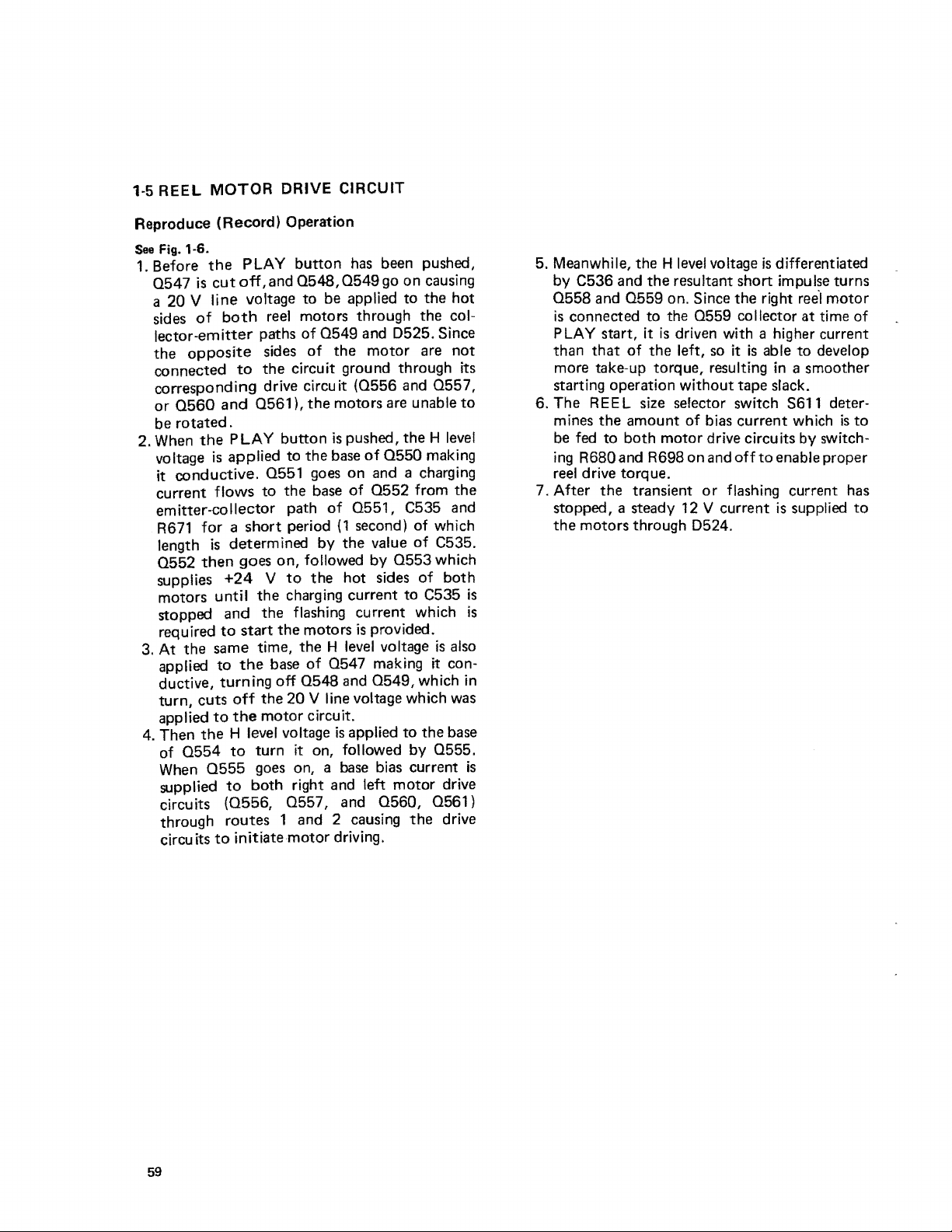
1-5 REEL
Reproduce (Record) Operation
See
Fig.
1. Before
0547
a
sides
lector-emitter
the
connected
corresponding
or
be
2. When
voltage
it
current
emitter-collector path
R671
length
Q552
supplies
motors until
stopped
required
3. At
applied
ductive, turning off
turn,
applied
4. Then
of Q554
When
supplied
circuits (Q556,
through
circuits
MOTOR
1-6.
the
is
cut
off,
20
V line voltage
of
both
opposite
to
Q560
and
rotated.
the
P
LA
is
applied
conductive.
flows
for a short
is
determ
then
goes
+24 V to
and
to
start
the
same time,
to
the
cuts
off
to
the
the
H level voltage
to
Q555
to
routes
to
initiatemotor
DRIVE CIRCUIT
PLAY
and
button
0548,
to
be applied to
reel motors through the col-
paths
of
0549
sides
of
the
the
circuit ground through its
drive circuit
0561
),
the
motors are unable
Y
button
to
0551
to
the
is
the
base
goes on and a charging
base
of
period
(1
ined by
on,
followed by
the
the
charging current
the
flashing current which
the
motors
the H level
base
of
0547
0548
the
20 V line voltage which was
motor circuit.
is
turn
it on, followed by
goes on, a base bias current
both
right and left motor drive
0557,
1 and 2 causing
driving.
has been pushed,
0549
go on causing
the
and D525. Since
motor
(0556
pushed,
of
of
0552
are
and
the H level
0550
making
from
0557,
Q551, C535 and
second) of which
the
value
of
C535.
0553
which
hat
sides
of
both
to
C535
is
provided.
voltage
is
making it con-
and
0549,
applied
to
which
the
0555.
and
0560,
the
Q561)
drive
hat
not
to
the
is
is
also
in
base
is
5. Meanwhile, the H
by C536 and
0558
and Q559 on. Since the right
is
connected to the
P
LA
Y start, it
than
that
of
more take-up torque, resulting
starting operation without
6. The
m ines
RE
E L size selector switch S611 deter-
the
amount
level
voltage
the
resultant short impulse turns
is
differentiated
ree·1
0559
collector
is
driven with a higher current
the
left, so it
is
tape
of
bias
current
at
able
to
in
a smoother
slack.
which
develop
be fed to both motor drive circu its by switching
R680 and R698 on and
off
to
enable proper
reel drive torque.
7. After
stopped, a steady 12 V current
the
the
transient
or
motors through D524.
flashing current has
is
supplied
motor
time
is
of
to
to
59
F'ROM
(H
LEVEL
PIN
12
OF'
OUR!NG
R660
C:534l
U5l9
PL.AYl
R679
0548
R664
R665
R698 R680
0553
0524
2ov-'T7
----HL_l2V
24V
20V
12V
PLAY
t DRIVE
24V
VOLTAGE
t-
R687
C536
0530
0554
Fig.
1-6
Reel
Motor
Drive
Circuit
RI GHT REEL
_
_,_
__
LEFT
MOTOR
AOOIT!ONAL
FRASHING
(
CURRENT
OUE
(l·~-
1 -
REEL
MOTOR
t-
60
1-6. TAPE
DIRECTION
COUNTER
CIRCUIT
See Fig.
This
which
stationary
This
1-7.
tape
deck
detect
and
function
whether
the
is
photo-interruptors,
and a
photo
transistor
transistor.
are
respectively
and lower sides
openings
shaft.
mounted
that
photo
disc
pair
pulses
higher
speed.
and
The
in
both
output
transistors
rotates
of
LEDs
output
the
The
is
second
a similar
and
and
pulse
pulse
photo-transistor
U517 (an
wave-shaped
amplifier/wave
pulse
SENSING AND
CLOCK GENERATION
employs
direction
performed
of a rotating
coupled
pulses produced
are
the
represent
frequency,
output
(PH502)
photo-sensing circuits
the
tape
is
running
each
The
pair
manner,
in which it
by
consisting
LED
mounted
disc
to
the
of
photo·couplers
but
is
two
of
and
the
on
the
which
right reel
in
such a way
by
90°
out
of
phase
when
openings pass between each
photo
transistors.
tape
speed,
the
obtained
is
applied
Thus,
higher
from
to
shaper} and
output
developed
at
or
running.
pairs
of
an LED
photo
upper
has
four
motor
the
two
the
the
and
the
the
tape
the
first
pin 2
of
the
pin 1
of
U517
then
flip-flop U505).
photo
then
same
same f!ip-flop.
(high,
pulses applied
high level
is
ning
when
The
turns
conductive
increment
counter
way,
tion,
DOWN
is
further
to
pin
transistor
to
pin 12
way
low}
output
in
forward direction and a low level
the
high level signal produced
on
UP/DOWN
when
the
low level
input termina I
as
applied
11
of
The
is
of
U505
the
pulse applied
The
U505
pulse
applied
after
f lip-flop
to
(the
output
to
relationship between
to
pins
11
and 12 and produces a
at
pin 9
when
tape
is
0532,
so
that
the
the
running
which
the
tape
input
tape
output
in
in
turn
instruction required
counter
terminal. In a similar
is
running
is
to
decrement
the
clock terminal
pin 6
wave-shaped
to
checks
the
reverse direction.
at
is
in
applied
base
of
0530,
by
the
second
of
U517,
in
pin
11
of
the
phase
the
tWQ
input
tape
is
output
pin 9
of
U505
makes
issued
0533
to
reverse direc-
to
the
the
of
the
the
run-
to
the
UP/
tape
counter.
FROM
PHOTO
COUPLER
tPH~02)
fROM
PHOTO
COVPLER
IPH5031
-,.5v
R584
.11.11.r~
R591
""UülJ7
6
5
U5!7
R588
R587
7
R594
R585
R586
R592
R593
Fig. 1-7. Tape Direction
R696
J711.
J"\I'JL
R595
R602
R603
R590
JV',
Sensing
vs,
~L.:;_1J7..::._S-_Rj,j.G,._O6 __
R598
L LEVEL
and
Tape Counter Clock Generation Circuit
TO
CLOCK
TAPE
COUNTER
R600
FOR FORWARD TAPE
FOR
REVESE
TAPE
INPUT
vss
RUNNlNG
RUNNI
Of
UNI
T
TO
UP/OOW!!
INPUT
TAPE
COUNTE~
NG
UNtT
CF
61
1-7.
COUNTER
See Fig. 1-7.
The wave-shaped pulse
1 of U517
turn
0528
pulse
output
lector
the
1-8.
See
electronic
MOTION
Fig. 1-8.
1.
The
U517
is
applied
wave-shaped pulse
to
ferentiated
of
0527
corresponding
Thus,
C523
CLOCK
PULSE
output
is
also
applied
on
or off, along with Q529.
thus
to
tape
to
the
obtained
the
at
clock input terminal of
counter as a clock pulse.
SENSING CIRCUIT
output
represent
by
to
turn
is
the
tape
C525, then applied
it
on
and off
to
the
tape
speed at
repeatedly charged and dis-
developed at pin
base of Q528
the
0529
from pin 7 of
speed
to
the
at
a frequency
that
charged. However, C523 does not charge
when
0527
high speed
or
goes
when
on
the
and
tape
off
is
running
repeatedly
speed, and pin 6 of U516 (comparator) goes
is
time.
at
to
The
col-
dif-
base
at
high
HIGH
the
running
HIGH and
the
2. Since
applied
and
and
U516 also
low speed as lang as
3.
The
so
that
pin 7 of U516 goes HIGH. On
other hand, pin 7 goes
at
low speed. (Pin 7 may develop
LOW
output
tape
runs
at
a threshold speed.)
the
voltage developed
to
the
base
0507,
off
0521
goes on
at
low speed. Consequently, pin 1 of
outputs H at
two signals obtained
U516 are used
as
LOW
when tape
in
alternation when
at
pin 7 of U516
of
Q521 through R566
at
high
tape
speeds
0520
high speed
is
off.
at
pins 7
and L at
and 1 of
motion control signals, as
described later.
4. The motion sensing circu it does not operate
in
the
PLAY and PAUSE modes because pin
12
(PLAY OUT) and pin
U519
are
connected
respectively, and
when
the
PLA Y
or
0526
PAUSE
to
11
0508
is
forced
button
(PAUSE) of
and
0509,
to
go
on
is
pushed.
is
is
+B
T0
PIN
1 PLAY
TO
PIN
!PAUSE OUT 1
H(F,F
ond
REW}
+5v
R696
R582
R581
0508
D509
C525
......
D510
R580
H:
fOR
(
L :
FOR
CONTROL SIGNAL
HIGHER
TAPE
LOWER
TAPE
RUNNING
RUNNING
CONTROl ~GMAl
H:
fOR
HiGHER
TAPE
)
(
L:
FOR
LOWER
Tt\l>E
RltlNiNG )
R\JNNING
.TU"\.
R594
12
OF
U5l9
OUTl
11
OF
U519
I
Fig. 1-8. Motion
Sensing
Circuit
62
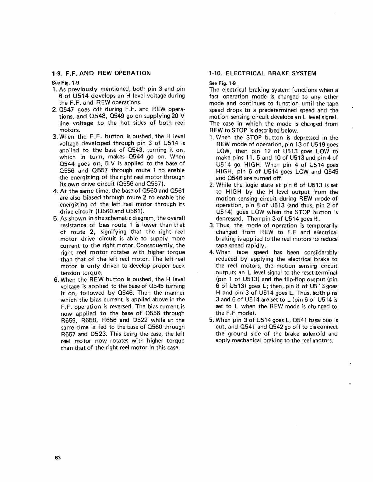
1-9. F.F. AND
See
Fig.
1-9
1.
As
previously
6
of
U514
the F
.F.
2.
0547
goes
tions, and
line voltage
REW
OPERATION
mentioned,
develops
both
an
H level voltageduring
and REW operations.
off
du ring F .F.
0548,
to
0549
the
go on supplying 20 V
hat
sides
motors.
3.
When
the F .F.
button
is
pushed, the H level
voltage developed through pin 3
applied
which in
0544
0556
the energizing
its
4.
At
own
the
to
goes
and
drive
same
the
turn,
an,
0557
circuit
time,
base
of
0543,
makes
5 V
is
applied
0544
thraugh raute 1
of
the right reel
(0556
the
base
are also biased through raute 2
energizing
drive
5.
As
shown
resistance
of
raute
motor
current
right reel
than
motor
tension
6.
When
voltage
it
on,
which the bias current
F .F. operation
now
R659, R658, R656 and
same
R657 and D523. This
reel
than
of
circuit
in
(0560
the
of
2,
drive
to
the
motor
that
of
the
is
only
torque.
the
REW
is
applied to the
followed
applied
time is fed
motor
that
now
of
the right
the left
and
reel
0561).
schematicdiagram, the overa!I
bias raute 1
signifying
circuit
is
that
able
right motor. Consequently, the
rotates
left
with
reel
motor. The
driven to develop proper back
button
is
pushed, the H level
base
by
0546.
is
applied above in the
is
reversed.
to
the
base
0522
to
the
base
being
rotates
reel
with
motor
pin 3 and pin
and
REW
opera-
of
both
reel
of
U514
turning
go
to
motor
and
0557).
of
0560
to
motor
is
lower than
the
to
supply more
it
on,
on. When
the
base
to
enable
through
and 0561
enable the
thraugh its
that
right
reel
higher torque
left
reel
of
0545
turning
Then the manner
The
bias
current
of
0556
thraugh
while
at
the
of
0560
thraugh
the
case,
the left
higher torque
in this
case.
is
of
is
1-10. ELECTRICAL BRAKE SYSTEM
See Fig. 1-9
The electrical braking system functions when a
fast operation mode
mode
and
continues
speed
draps
to
motion
The
REW
1.
case
to
When
REW
sensing
circuit develops an L level signal.
in which the mode
STOP
is
the
STOP
mode
of
LOW, then pin 12
make pins 11, 5
U514
go
HIGH.
HIGH, pin 6
and
0546
are turned
2. While the logic state at pin 6
to
HIGH
motion
by
sensing
operation, pin 8
U514)
goes
LOW
depressed. Then pin 3
3. Thus, the mode
changed
braking
tape
4.
When
reduced
the
outputs
(pin 1
6
of
H and pin 3
3
and 6 of
set
the F
5.
When
cut,
the ground
from
is
applied
speed
rapidly.
tape
by
applying the electricai'hrake
reel
motors, the motion
an L level
of
U513)
U513)
goes
of
U514
to
L when the R
.F
mode).
pin 3
of
and
0541
side
apply mechanical braking
is
changed
to
function
a predetermined
described below.
button
is
operation, pin 13
of
U513
and
10
of
U513
of
When
U514
pin 4
goes
off.
the H level
output
circuit during
of
U513
(and
when the
of
U514
of
operation
REW
to F.F
to
the
reel
motors
speed
has
been
signal
to the
and
the
flip-flopoutput
L;
then, pin 8
U514
goes
are
set
to
L (pin 6
EW
mode
U514
goes
L,
and
0542
go
of
the brake sole~oid
to
L.
0541
off
the
to
any other
until
speed
is
changed
depressed
of
U519
goes
and
of
U514
LOW and
of
U513
from
REW
mode
thus,
pin 2 of
STOP
button
goes
f-1.
is
temporarily
and
electrical
10
considerably
sensing
reset
terminal
of
U513goes
Thus,
both
of
is
cha
base
to
disconnect
reel
rnotors.
the tape
and
the
from
in
the
goes
LOW
to
pin 4
of
goes
0545
is
set
the
of
reduce
to
circuit
(pin
pins
U514
is
nged
to
bias
and
is
is
63
U512
+SV +12V
U519
REW
FROM
MOTION H
SENSING CIRCUIT L
(PIN 7 OF
"H"
"H"
R648
R649
R652
516)
LEVEL
LEVEL
FOR
FOR
FF
REW
R650
FOR
HIGH SPEED
FOR
LOW
SPEED
R651
R655
+B
+B
1
1
1
1
\0544
,
(
f -
1
1
R658
1
1
1
1 R659
1
1
T
+24V
R686
R683
D532 D533
R653
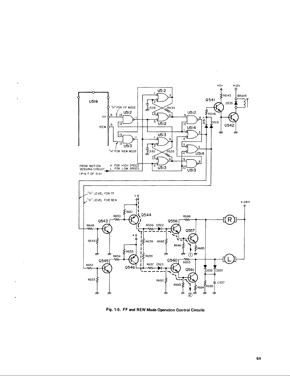
Fig. 1-9.
FF
and
REW Mode Operation Control Circuits
R694
C537
R696I
64
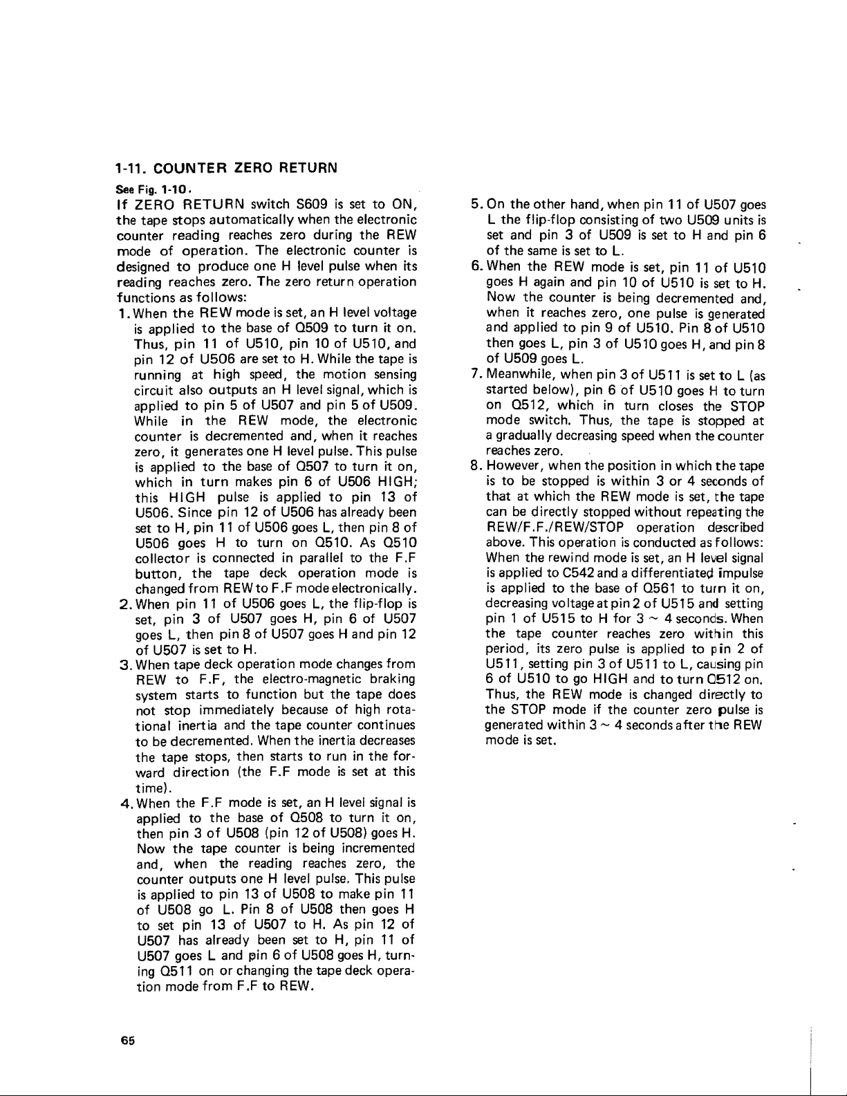
1-11.
See
lf
Fig.
ZERO
COUNTER
1-10,
RETURN
ZERO RETURN
switch S609
is
set
to
ON,
the tape stops automatically when the electronic
counter reading
mode
designed
of
operation.
to
reaches
zero during the
The electronic counter
produce one H
level
pulse when its
REW
reading reaches zero. The zero return operation
functions
1.
When
is
Thus,
pin 12
running at high
circuit also
applied
While
counter
zero,
is
which
this
U506. Since
set
U506
collecto r
button,
changed
2.
When
set,
goes
of
3.
When
REW
system starts
not stop immediately
tiona l inertia
to
the tape stops, then starts
ward
as
follows:
the
REW mode
applied
pin
of
to
the
11
of
U506
outputs
to
pin 5 of
in
the
is
decremented and, when
it
generates one H level pulse. This pulse
applied
in
HIGH
to
turn
pulse
the
pin
to
H,
pin
11
goes H to
is
connected in parallel to the F .F
is
base
of
U510, pin
are
set
speed,
an
U507
REW
base
of
makes
is
applied
12
of
of
U506
turn on
set,
an
H level voltage
0509
to
10
of
to
H. While the tape
the motion
H level signal, which
and
pin 5
mode, the electronic
0507
to
pin 6
of
to
U506
has
goes
L, then pin 8
0510.
the tape deck operation mode
from
REW
to
F .F mode electronically.
pin
11
of
U506
goes
L, the
pin 3 of
L, then
U507
is
set
U507
pin 8 of
to
H.
goes
U507
H, pin 6
goes
tape deck operation mode
to
F.F, the electro-magnetic braking
to
function but the tape
because
and
the tape counter continues
be
decremented.
direction
When
the inertia
to
(the F.F mode
run in the for-
turn
it
on.
U510,
and
sensing
of
U509.
it
reaches
turn
it
on,
U506 HIGH;
pin 13
atready
of
been
of
As
0510
flip-flop
of
U507
Handpin
changes
12
from
does
of
high rota-
decreases
is
set
at this
time).
4.
When
the F .F mode
applied
then
Now
to
the
pin 3 of
the
tape counter
U508 (pin
and, when the reading
counter outputs one H
is
applied
of
U508
to
set
U507
U507
ing
tion mode
to
go
pin 13
has
already
goes L and
0511 on
from F .F
pin
L.
or
is
set,
base
13
of
Pin 8 of
of
U507
been
r,in 6
an H level
of
0508
12
of
is
being incremented
reaches
level
pulse. This pulse
U508
to
U508 then
to
H.
set
to
of
U508
to
turn
U508)
zero, the
make pin
As
pin
H, pin
goes
H, turn-
signal
it
goes
goes
12
11
changing the tape deck opera-
to R EW.
is
on,
H.
11
H
of
of
is
is
is
is
is
5.
On
the other hand, when pin
L the
flip-flop
set
and
of
the
6.
When
goes H again
Now
the counter
when
it
and applied
then
goes
of
U509
same
the
pin 3
is
REW
and pin
reaches
to
L, pin 3
goes
consisting
of
U509
set
to
L.
mode
10
is
being decremented and,
zero, one pulse
pin 9
of
of
U510
L.
7. Meanwhile, when pin 3
started below), pin 6
on
0512,
which in turn
of
mode switch. Thus, the tape
a gradually
reaches
decreasing
zero.
speed
8. However, when the position in which
is
to
be
that
at which the
can
be
stopped
directly
is
within
REW
stopped
11
of
of
two
U509 units
is
set
to H and
is
set, pin
of
U510
U510. Pin 8
goes
of
U511
is
U510
goes H to
closes
is
when the
3 or 4
mode
is
set, the tape
without
repeating the
U507
11
of
is
set
is
generated
of
H,
and
set
to L (as
the
stopped at
eo
the
seconds
REW/F.F./REW/STOP operation described
above. This operation
When
the rewind mode
is
applied
is
applied
to
to
C542
the
decreasing voltage at pin 2
pin 1
of
U515 to H
the tape counter
period, its zero pulse
U511, setting pin 3
6
of
U510
to
go
Thus, the
the
generated
mode
STOP
is
set.
REW
mode
within
is
conducted
is
set,
and
a differentiated impulse
base
of
0561
of
for
3 ~ 4 seconds.
reaches
of
HIGH
mode
if
the counter zero pulse
3 ~ 4
zero
is
applied
U511
and
is
changed
seconds
an
H level
to
U515
to p in 2 of
to
L,
to
turn
after
as
turn
and
wittlin
causing pin
directly
follows:
0512
the
goes
pin 6
U510
to
H.
U510
pin 8
turn
STOP
unter
tape
of
signal
it
on,
setting
When
this
on.
to
REW
is
is
65
ZD
(FROM
COUNTER
ZERO
RETURN
SW
S609
R525
H(F.Fl
R529
FR0M U519
PIN15
H(REW)
R532
FR0M U519
PIN13
ELECTR0NICS\
+5V
C516r
C514l
C515l
R709
R707
H:HIGH
L:
L0W SPEED
FR0M
(
PIN I 0F
Fig.
1-10. Counter Zero Return Control Circuit
C543r
SPEED
SENSING
CIRCUIT)
66
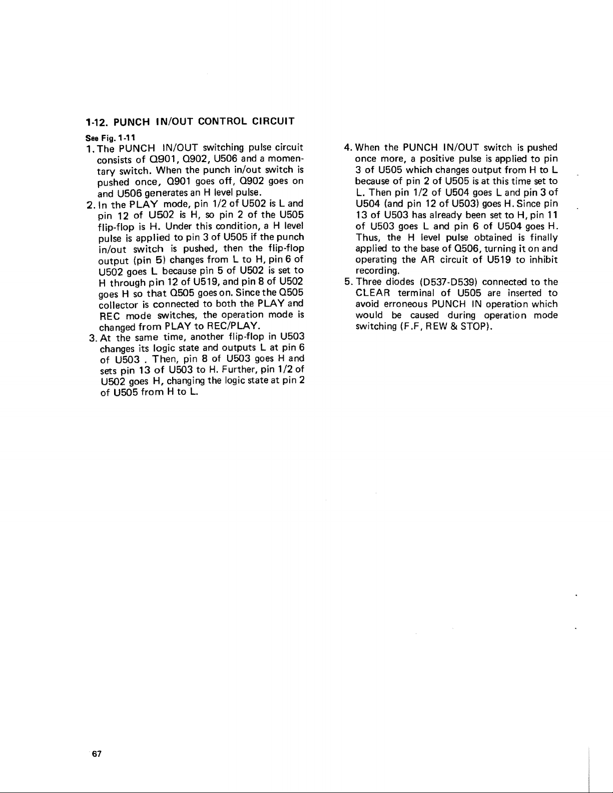
1-12. PUNCH
See Fig. 1-11
1. The PUNCH
consists
tary
switch. When the punch
pushed once, 0901
and
U506 generates
2. In
the
pin 12
flip-flop
pulse
is
in/out
output
U502
H through
goes H so
collector
REC
changed
3.
At
the
changes
of
U503 . Then, pin 8
sets
pin 13
U502
of
U505
IN/OUT
of
0901,
PLAY
of
U502
is
H.
applied
switch
(pin
5)
goes L because
pin
that
is
connected
mode switches, the operation mode
from
same
its logic state
of
goes
H,
from H to
CONTROL CIRCUIT
IN/OUT
mode, pin 1/2
Under this condition, a H
is
changes
12
0505
PLAY
time, another flip-flop in U503
U503
changing the logic state at pin 2
switching pulse circuit
0902,
is
to
pushed, then the
of
U506
goes
off,
an H level
H,
so
pin 2
pin 3
of
from L
pin 5
U519,
goes
on. Since the
to
both the PLA Y
to
REC/PLAY.
and
of
to
H.
in/out
pulse.
of
U505
of
and
outputs L at pin 6
U503
Further, pin
and
0902
U502
of
if
to
H, pin 6
U502
pin 8
goes
a momen-
switch
goes
on
is
Land
the U505
level
the punch
flip-flop
of
is
set
to
of
U502
0505
and
H and
1/2
of
L.
is
is
4.
When
the PUNCH
once more, a positive pulse
3
of
U505 which
because
L.
U504
13
of
Thus, the H level
applied to the
operating the AR circuit
recording.
5. Three diodes (0537-0539) connected
CLEAR terminal
avoid erroneous PUNCH IN operation which
would be
switching (F.F,
of
pin 2
Then pin 1/2
(and
pin 12
of
U503
has
U503
goes
caused
IN/OUT
changes
of
U505
of
U504
of
U503)
already
L and pin 6
pulse
base
of
of
during operation mode
REW
& STOP).
output
is
goes
been
obtained
0506,
of
U505
switch
is
applied
at this time
Land
goes
set
of
U504
turning
U519
are
is
pushed
from
pin 3
H. Since pin
to
H, pin
goes
is
it
on and
to
inserted
to
pin
H to L
set
to
of
11
H.
finally
inhibit
to
the
to
67
12
PLAY
(>-"
=----..--------------------~
PUNCH
IN/OUT
SWITCH
AR
R902
R901
h
l
U519
REG
+5V
R516
STOP
F.
U506 REW
3
(H)
_n_
1
2
U502
SW,
F.
SW.
SW.
Fig. 1·11.
D537
0538
0539
U504
R519
Punch
R520
3
4
In/Out
Control Circuit
U503
PLAY
(5601)
PLAY
(S605)
TO
AR OF U519
(1)
00
1-13.
EDIT
See
control section
1.
When
go an,
an,
ly
power supply
DC
actuate
also
the
2.
At
the
CONTROL CIRCUIT
of
the inserted circuit diagrams.
the
EDIT
switch
followed
the
Q813
by
base
is
power
goes
the
to
the capstan
motor.
on
to
STOP mode.
same
time, when Q509
is
Q512. With Q512 turned
bias
circuit on
closed and Q813 supplies
At
the
turn
off
and Q558 are grounded through
0529
and through the collector-emitter path
of
Q509,
3. Ouring the
or
and R EW IN circuits
switch being
to
stop the take-up
EDIT
REW mode
set
mode
is
available
on.
of
are
on, Q509 and Q510
PCB
assemb-
motor
same
Q514
reel
operation,
because
opened
time,
goes
0528,
motor.
the F.F IN
by
circuit
to
Q511
to
release
an, Q556,
0527,
no
F.F
the
ED
IT
+24V
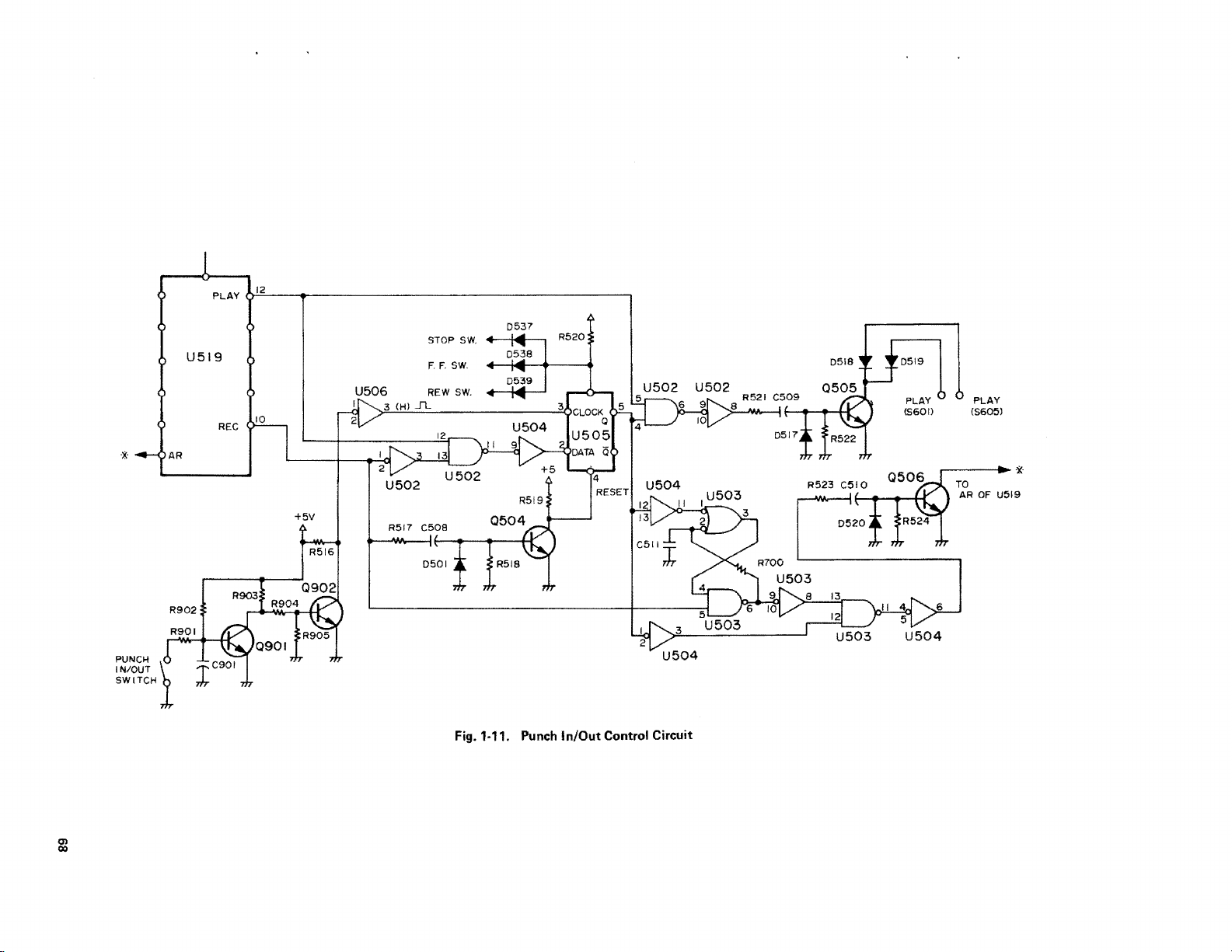
1-14.
REC
AND PLAY MUTE SIGNALS
See
Fig. 1-12.
1.
REC
signal
When the
U519
applied
When Q524
and Q525
connected
to
actuate amplifier circuits associated
REC
outputs
to
the
goes
also
to
button
goes
R579
recording.
2. Play Mute Signal
When
of
applied
grounding the
the
PLA
Y button
U519 outputs
to
the
PLAY
low level state
amplifier circuit
switch connected in parallel
the
same
function
when
it
is
closed.
5607
CUE
---+-2-4V.J~
is
depressed, pin
an H level
base
of
an, Q525
signal, which
Q524
to
base
on. The +24 V line
for
use
as
a contro I voltage
is
depressed, pin
an H level
base
of
signal, which
Q534
to
MUTE terminal. This
is
also
used
to control the
(as
described later). The
with
as
the
PLAY
10
of
is
turn
it
on.
current flows
is
then
with
12
is
turn
it
on,
CUE
Q534
serves
MUTE
signal
U519
REC
10
R695
C528
l
R576
R722
Fig. 1-12.
R608
.__.,__
I
R578
Rec
& Play Mute Circuit
R609
__
C529
+24V
REC
R827
.,___..._~--
SIG
R828
PLAY MUTE
69
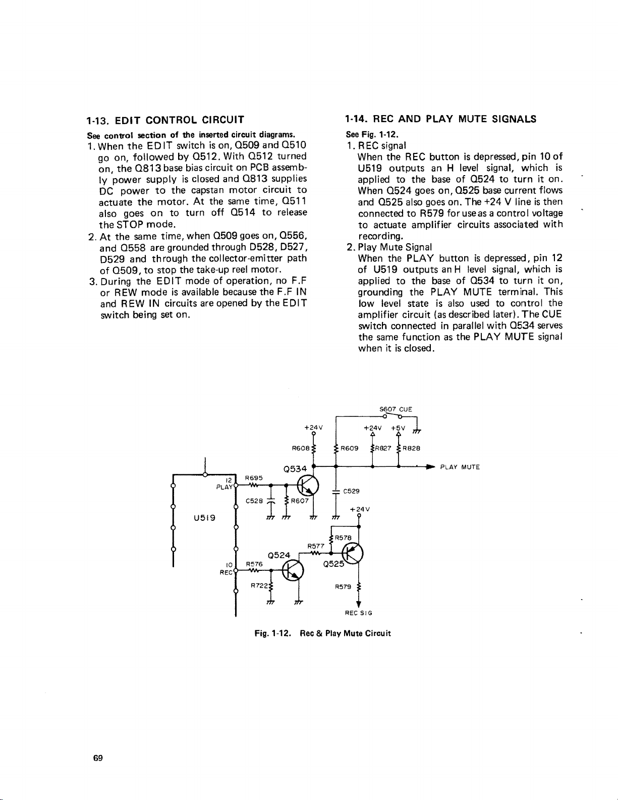
1·15.
DISPLAY
See
Fig.
1-13.
A.RECORD
1. The
comparator
and
7 const itutes a square
and
outputs a pulse
REC
button
to H and
of
U511.
pin 5
of
is
on, pin 1
2.
lf
one
mitches
applied to R511
causing
H.
pin 11
Then,
L, setting p
0501 on.
3.
Next, assume that none of the record
LED
is
the
pulse
The
0501.
of
or
more
are
mitched
pin 3 of
in 6 of
Thus,
CIRCUIT
of
U515
signal
at pin 7.
depressed, pin 9
output
pulse signal
Meanwhile,
U501
is
is
as
is
set
to H.
of
the record function
on, a L
as
the
REC
of
U511 (pin 2
U501 (pin 4
U501 to H
the
REC
LED (D601) lights.
with
pins 5, 6,
wave
oscillator
When
of
U511
obtained at pin 8
then fed
the
REC
level
signal
MODE signal,
of
U501)
of
U501)
and
turning
+5V
the
is
set
to
gate
button
to
go
goes
is
function switches
then applied
R511
so
that
goes
L.
Since pin 1
3
of
U501 (pin 4
output
gate (pin 6
are
to
pins 12/13
pin
11
of
of
on;
of
U511 (pin 2
of
U501
U501)
U501) opens. Then, the
pulse signal applied to pin 5
output
and
indicate
mode
from pin 6
oft
and
that
but
that
of
U501, turning
making the
the tape deck
no recording channel is design-
ated.
B.
PAUSE LED
When
on, pins 12
an L level
Then, pin 8
and
the
REC
and
the
PAUSE
and
13
of
U501
signal
is
output
of
U501
goes
lighting PAUSE LED D602.
an
H level
of
U511 through
is
set
goes H and
of
REC
LED flash to
is
in
buttons
are
set
at pin
11
H, turning
signal
of
501)
to
H, pin
the
U501
0501
on
the R EC
are
to
Hand
of
U501.
on
0502
is
is
L (REC
MODE)
PAUSE
U519
PLAY
REC
12
II
IQ
Fig.
R556
R557
1-13.
C552
r
Display
R716
R559
Circuit
+24V
REC
Q50I
D602~
+24'/
R558
70
1-16.
AMPLI
This
description
the
exception
are assembled
TER OSC
LED
indicators.
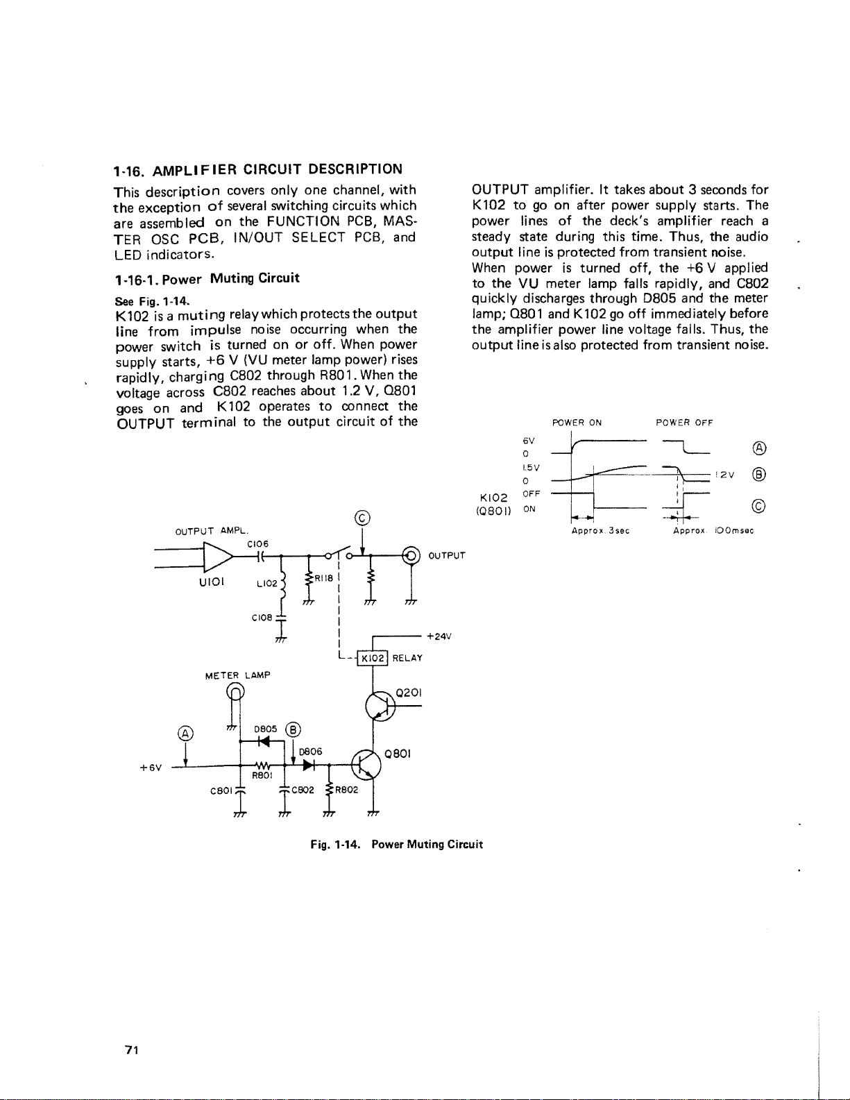
1-16-1.
See Fig. 1-14.
K102
is a muting
line
from
power switch is turned
supply starts,
F IER CIRCUIT DESCRIPTION
PCB,
Power
covers only
of
several switching circuits which
on
the
IN/OUT SELECT PCB, and
Muting Circuit
one
FUNCTION
relaywhich protects
impulse
+6
noise occurring when
an
or
off. When power
V
{VU
meter lamp power) rises
channel, with
PCB,
the
output
rapidly, charging C802 through R801. When
voltage across
goes
on
OUTPUT
C802
and
K 102 operates
terminal
reaches
to the
about
to
output
1.2 V,
connect
circuit
©
OUTPUT
~1-6
AMPL.
___
11
.,.._-crJ
MAS-
the
the
0801
the
of
the
OUTPUT
OUTPUT amplifier. lt takes
K 102
to
go
an
after power supply starts. The
power lines
of
the
about
3 seconds for
deck's amplifier reach a
steady state during this time. Thus,
output
When power
to
quickly discharges through
lamp;
the
output
(Q801)
line
is
protected from transient noise.
is
the
turned off,
VU
meter lamp falls rapidly, and C802
0801
and K102 go off immediately before
the
0805
+6 V applied
and
amplifier power line voltage falls. Thus,
line
is
also protected from transient noise.
POWER
Ki02
6V
0
15V
0
OFF
ON
ON
Appro
x.
3sec
POWER OFF
'""7_
~12V
, ,
~
Approx.
the
the
IOOmsec
audio
meter
the
®
@
©
+6V
®
UIOI
METER
Cl08l
LAMP
""
l
1
1
1
1
L_
Fig.
R802
1-14.
1C802
Power
Muting Circuit
71
 Loading...